US7768128B2 - Semiconductor memory devices including a damascene wiring line - Google Patents
Semiconductor memory devices including a damascene wiring line Download PDFInfo
- Publication number
- US7768128B2 US7768128B2 US11/499,059 US49905906A US7768128B2 US 7768128 B2 US7768128 B2 US 7768128B2 US 49905906 A US49905906 A US 49905906A US 7768128 B2 US7768128 B2 US 7768128B2
- Authority
- US
- United States
- Prior art keywords
- insulating layer
- interlayer insulating
- lower wiring
- wiring lines
- integrated circuit
- Prior art date
- Legal status (The legal status is an assumption and is not a legal conclusion. Google has not performed a legal analysis and makes no representation as to the accuracy of the status listed.)
- Expired - Fee Related, expires
Links
- 239000004065 semiconductor Substances 0.000 title description 23
- 239000010410 layer Substances 0.000 claims abstract description 121
- 239000011229 interlayer Substances 0.000 claims abstract description 91
- 239000000758 substrate Substances 0.000 claims abstract description 37
- 230000004888 barrier function Effects 0.000 claims description 11
- 238000000034 method Methods 0.000 description 28
- 230000008569 process Effects 0.000 description 19
- 230000003667 anti-reflective effect Effects 0.000 description 18
- 239000010949 copper Substances 0.000 description 16
- 229920002120 photoresistant polymer Polymers 0.000 description 14
- RYGMFSIKBFXOCR-UHFFFAOYSA-N Copper Chemical compound [Cu] RYGMFSIKBFXOCR-UHFFFAOYSA-N 0.000 description 13
- 229910052802 copper Inorganic materials 0.000 description 13
- 238000005530 etching Methods 0.000 description 12
- 238000009792 diffusion process Methods 0.000 description 10
- 239000000463 material Substances 0.000 description 10
- 238000002955 isolation Methods 0.000 description 8
- 239000007769 metal material Substances 0.000 description 7
- 239000005380 borophosphosilicate glass Substances 0.000 description 6
- 238000000151 deposition Methods 0.000 description 6
- 239000012535 impurity Substances 0.000 description 6
- 238000004519 manufacturing process Methods 0.000 description 6
- 239000005360 phosphosilicate glass Substances 0.000 description 6
- 239000011368 organic material Substances 0.000 description 4
- 229920003209 poly(hydridosilsesquioxane) Polymers 0.000 description 4
- 229910000838 Al alloy Inorganic materials 0.000 description 3
- OKTJSMMVPCPJKN-UHFFFAOYSA-N Carbon Chemical compound [C] OKTJSMMVPCPJKN-UHFFFAOYSA-N 0.000 description 3
- PXGOKWXKJXAPGV-UHFFFAOYSA-N Fluorine Chemical compound FF PXGOKWXKJXAPGV-UHFFFAOYSA-N 0.000 description 3
- 230000015572 biosynthetic process Effects 0.000 description 3
- 229910052799 carbon Inorganic materials 0.000 description 3
- 239000004020 conductor Substances 0.000 description 3
- 230000008021 deposition Effects 0.000 description 3
- 229910052731 fluorine Inorganic materials 0.000 description 3
- 239000011737 fluorine Substances 0.000 description 3
- 229910052751 metal Inorganic materials 0.000 description 3
- 239000002184 metal Substances 0.000 description 3
- 238000000206 photolithography Methods 0.000 description 3
- 125000006850 spacer group Chemical group 0.000 description 3
- VYPSYNLAJGMNEJ-UHFFFAOYSA-N Silicium dioxide Chemical compound O=[Si]=O VYPSYNLAJGMNEJ-UHFFFAOYSA-N 0.000 description 2
- 229910004200 TaSiN Inorganic materials 0.000 description 2
- 229910008482 TiSiN Inorganic materials 0.000 description 2
- ATJFFYVFTNAWJD-UHFFFAOYSA-N Tin Chemical compound [Sn] ATJFFYVFTNAWJD-UHFFFAOYSA-N 0.000 description 2
- 238000010586 diagram Methods 0.000 description 2
- 238000001312 dry etching Methods 0.000 description 2
- 230000009977 dual effect Effects 0.000 description 2
- 238000007772 electroless plating Methods 0.000 description 2
- 238000009713 electroplating Methods 0.000 description 2
- QRXWMOHMRWLFEY-UHFFFAOYSA-N isoniazide Chemical compound NNC(=O)C1=CC=NC=C1 QRXWMOHMRWLFEY-UHFFFAOYSA-N 0.000 description 2
- 125000002496 methyl group Chemical group [H]C([H])([H])* 0.000 description 2
- 229920006254 polymer film Polymers 0.000 description 2
- 239000005368 silicate glass Substances 0.000 description 2
- 229910052814 silicon oxide Inorganic materials 0.000 description 2
- 238000001039 wet etching Methods 0.000 description 2
- XUIMIQQOPSSXEZ-UHFFFAOYSA-N Silicon Chemical compound [Si] XUIMIQQOPSSXEZ-UHFFFAOYSA-N 0.000 description 1
- 229910052782 aluminium Inorganic materials 0.000 description 1
- XAGFODPZIPBFFR-UHFFFAOYSA-N aluminium Chemical compound [Al] XAGFODPZIPBFFR-UHFFFAOYSA-N 0.000 description 1
- 230000000694 effects Effects 0.000 description 1
- 239000011521 glass Substances 0.000 description 1
- 239000011810 insulating material Substances 0.000 description 1
- 230000005012 migration Effects 0.000 description 1
- 238000013508 migration Methods 0.000 description 1
- 238000012986 modification Methods 0.000 description 1
- 230000004048 modification Effects 0.000 description 1
- 230000003647 oxidation Effects 0.000 description 1
- 238000007254 oxidation reaction Methods 0.000 description 1
- 238000005498 polishing Methods 0.000 description 1
- 229910052710 silicon Inorganic materials 0.000 description 1
- 239000010703 silicon Substances 0.000 description 1
Images


Classifications
-
- H—ELECTRICITY
- H10—SEMICONDUCTOR DEVICES; ELECTRIC SOLID-STATE DEVICES NOT OTHERWISE PROVIDED FOR
- H10B—ELECTRONIC MEMORY DEVICES
- H10B10/00—Static random access memory [SRAM] devices
- H10B10/12—Static random access memory [SRAM] devices comprising a MOSFET load element
-
- H—ELECTRICITY
- H01—ELECTRIC ELEMENTS
- H01L—SEMICONDUCTOR DEVICES NOT COVERED BY CLASS H10
- H01L21/00—Processes or apparatus adapted for the manufacture or treatment of semiconductor or solid state devices or of parts thereof
- H01L21/02—Manufacture or treatment of semiconductor devices or of parts thereof
- H01L21/04—Manufacture or treatment of semiconductor devices or of parts thereof the devices having potential barriers, e.g. a PN junction, depletion layer or carrier concentration layer
- H01L21/18—Manufacture or treatment of semiconductor devices or of parts thereof the devices having potential barriers, e.g. a PN junction, depletion layer or carrier concentration layer the devices having semiconductor bodies comprising elements of Group IV of the Periodic Table or AIIIBV compounds with or without impurities, e.g. doping materials
- H01L21/30—Treatment of semiconductor bodies using processes or apparatus not provided for in groups H01L21/20 - H01L21/26
- H01L21/31—Treatment of semiconductor bodies using processes or apparatus not provided for in groups H01L21/20 - H01L21/26 to form insulating layers thereon, e.g. for masking or by using photolithographic techniques; After treatment of these layers; Selection of materials for these layers
- H01L21/3205—Deposition of non-insulating-, e.g. conductive- or resistive-, layers on insulating layers; After-treatment of these layers
-
- H—ELECTRICITY
- H01—ELECTRIC ELEMENTS
- H01L—SEMICONDUCTOR DEVICES NOT COVERED BY CLASS H10
- H01L21/00—Processes or apparatus adapted for the manufacture or treatment of semiconductor or solid state devices or of parts thereof
- H01L21/70—Manufacture or treatment of devices consisting of a plurality of solid state components formed in or on a common substrate or of parts thereof; Manufacture of integrated circuit devices or of parts thereof
- H01L21/71—Manufacture of specific parts of devices defined in group H01L21/70
- H01L21/768—Applying interconnections to be used for carrying current between separate components within a device comprising conductors and dielectrics
- H01L21/76801—Applying interconnections to be used for carrying current between separate components within a device comprising conductors and dielectrics characterised by the formation and the after-treatment of the dielectrics, e.g. smoothing
- H01L21/76802—Applying interconnections to be used for carrying current between separate components within a device comprising conductors and dielectrics characterised by the formation and the after-treatment of the dielectrics, e.g. smoothing by forming openings in dielectrics
- H01L21/76807—Applying interconnections to be used for carrying current between separate components within a device comprising conductors and dielectrics characterised by the formation and the after-treatment of the dielectrics, e.g. smoothing by forming openings in dielectrics for dual damascene structures
- H01L21/76808—Applying interconnections to be used for carrying current between separate components within a device comprising conductors and dielectrics characterised by the formation and the after-treatment of the dielectrics, e.g. smoothing by forming openings in dielectrics for dual damascene structures involving intermediate temporary filling with material
-
- H—ELECTRICITY
- H01—ELECTRIC ELEMENTS
- H01L—SEMICONDUCTOR DEVICES NOT COVERED BY CLASS H10
- H01L27/00—Devices consisting of a plurality of semiconductor or other solid-state components formed in or on a common substrate
- H01L27/02—Devices consisting of a plurality of semiconductor or other solid-state components formed in or on a common substrate including semiconductor components specially adapted for rectifying, oscillating, amplifying or switching and having potential barriers; including integrated passive circuit elements having potential barriers
- H01L27/0203—Particular design considerations for integrated circuits
- H01L27/0207—Geometrical layout of the components, e.g. computer aided design; custom LSI, semi-custom LSI, standard cell technique
-
- H—ELECTRICITY
- H10—SEMICONDUCTOR DEVICES; ELECTRIC SOLID-STATE DEVICES NOT OTHERWISE PROVIDED FOR
- H10B—ELECTRONIC MEMORY DEVICES
- H10B10/00—Static random access memory [SRAM] devices
Definitions
- the present invention relates to integrated circuit (semiconductor) memory devices and methods of fabricating the same, more particularly, to semiconductor memory devices which are capable of obtaining a process margin with improved electrical characteristics, and methods of fabricating the same.
- an associated design rule may be reduced.
- a RC delay effect on device performance may increase due to an increase of the resistance and the capacitance of a wiring line formed on the device. This increase RC delay may, in turn, lower the operating speed of the device.
- an interlayer insulating layer having a lower dielectric rate and wiring line materials having a lower resistance For example, copper (Cu), rather than aluminum alloy, may be used as a wiring line material, as copper has lower specific resistance than the conventional aluminum alloy. In addition, copper typically has a smaller electrical migration than the conventional aluminum alloy.
- the wiring line is generally formed by a damascene process.
- a dual damascene process which forms a via and a trench in the interlayer insulating layer and forms the wiring line by burying copper in the via and the trench has been used as a damascene process.
- a method of forming the trench after formation of the via may be used.
- a corner of the via may collapse, thereby generated a sloped region in the via.
- the lower wiring line may be exposed, which may cause the lower wiring line and an upper wiring line to be shorted.
- Some embodiments of the present invention provide integrated circuit memory devices including an integrated circuit substrate and a plurality of lower wiring lines on the substrate and extending in a first direction.
- An interlayer insulating layer is on the plurality of lower wiring lines.
- An upper damascene wiring line is in an upper portion of the interlayer insulating layer and extends in a second direction, different from the first direction, over the plurality of lower wiring lines.
- the upper damascene wiring line has protruded regions extending therefrom in a direction different from the second direction, the protruded regions extending over respective underlying ones of the lower wiring lines.
- a first via extends through the interlayer insulating layer under a first of the protruded regions and connects the upper damascene wiring line to a corresponding underlying first one of the plurality of wiring lines.
- a second via extends through the interlayer insulating layer under a second of the protruded regions and connects the upper damascene wiring line to a corresponding underlying second one of the plurality of wiring lines.
- the first and second protruded regions may each extend in a same direction or may extend in opposite directions.
- the interlayer insulating layer is a first interlayer insulating layer and the device further includes a plurality of first active regions in the integrated circuit substrate and a plurality of second active regions in the integrated circuit substrate, the second active regions having a conductivity type different from a type of the first active regions.
- a first gate electrode on the integrated circuit substrate intersects a first one of the first active regions and a first one of the second active regions.
- a second gate electrode on the integrated circuit substrate intersects a second one of the first active regions and a second one of the second active regions.
- a second interlayer insulating layer is on the substrate in a region including the first and second gate electrode and extends over the first and second gate electrodes.
- the plurality of lower wiring lines and the first insulating layer are on the second insulating layer.
- a first via extends through the second interlayer insulating layer and connects the first one of the plurality of lower wiring lines to the first gate electrode.
- a second via extends through the second interlayer insulating layer and connects another one of the plurality of lower wiring lines to the second gate electrode.
- the another one of the plurality of lower wiring lines is a third one of the plurality of wiring lines, different from the second one of the plurality of wiring lines.
- the second one of the plurality of lower wiring lines may connect ones of the first active regions and the second active regions to each other.
- the first, second and third ones of the plurality of lower wiring lines may extend substantially parallel to one another.
- the first active regions and the second active regions may be divided into two parts, respectively.
- a third gate electrode may be provided that intersects the first and second ones of the first active regions.
- the device may be a CMOS memory device and the type of the first active regions may be one of n-type or p-type and the type of the second active regions may be the other of n-type or p-type.
- Methods of fabricating an integrated circuit memory device are provided.
- Lower wiring lines are formed on an integrated circuit substrate extending in a first direction.
- An interlayer insulating layer is formed on the substrate including the lower wiring lines.
- a first via hole is formed that exposes a first of the lower wiring lines and a second via hole is formed that exposes a second of the lower wiring lines in the interlayer insulating layer by selectively etching the interlayer insulating layer.
- a trench is formed in an upper portion of the interlayer insulating layer, the trench extending in a second direction, different from the first direction, to extend over the lower wiring lines.
- the trench has protruded regions extending therefrom in a direction different from the second direction.
- the protruded regions extend over respective underlying ones of the lower wiring lines, ones of the protruded regions overlying and being connected on a bottom thereof to a corresponding underlying one of the first and second via holes.
- a conductive film is formed filling the via holes and the trench.
- a damascene wiring line is formed in the interlayer insulating layer by flattening the formed conductive film.
- the interlayer insulating layer is a first interlayer insulating layer and the method further includes forming a plurality of first active regions in the substrate and forming a plurality of second active regions in the substrate, the second active regions having a type different from a type of the first active regions.
- a first gate electrode is formed on the substrate that intersects a first one of the first active regions and a first one of the second active regions.
- a second gate electrode is formed on the substrate that intersects a second one of the first active regions and a second one of the second active regions.
- a second interlayer insulating layer is formed on the substrate in a region including the first and second gate electrode and extending over the first and second gate electrodes, wherein the lower wiring lines and the first insulating layer are on the second insulating layer.
- a first via is formed extending through the second interlayer insulating layer that connects one of the plurality of lower wiring lines to the first gate electrode and a second via is formed extending through the second interlayer insulating layer that connects another one of the plurality of lower wiring lines to the second gate electrode.
- the lower wiring lines include a first lower wiring line which is connected to the first gate electrode, a second lower wiring line through which the first active regions and the second active regions are connected to the second gate electrode, and a third lower wiring line through which the first active regions and the second active regions are connected to each other.
- the first lower wiring line through the third lower wiring line may extend substantially parallel to one another.
- the first lower wiring line and the third lower wiring line may be connected to each other by the damascene wiring line.
- the first active regions and the second active regions may be divided into two parts, respectively.
- a third gate electrode may be formed that intersects the first and second ones of the first active regions.
- FIG. 1 is a layout view illustrating a memory device according to some embodiments of the invention.
- FIG. 2 is a cross-sectional view illustrating the memory device of FIG. 1 taken along the lines I-I′ and II-II′ of FIG. 1 ;
- FIGS. 3 to 7 are cross-sectional views illustrating methods of fabricating a memory device according to some embodiments of the present invention.
- FIG. 8 is a circuit diagram illustrating a memory device according to further embodiments of the present invention.
- FIG. 9 is a layout view illustrating a memory device according to other embodiments of the present invention.
- FIG. 10 is a cross-sectional view illustrating the memory device of FIG. 9 taken along the lines III-III′ and IV-IV′ of FIG. 9 ;
- FIGS. 11 to 17 are layout and cross-sectional views illustrating methods of fabricating a memory device according to further embodiments of the present invention.
- first, second, etc. may be used herein to describe various elements, components, regions, layers and/or sections, these elements, components, regions, layers and/or sections should not be limited by these terms. These terms are only used to distinguish one element, component, region, layer or section from another region, layer or section. Thus, a first element, component, region, layer or section discussed below could be termed a second element, component, region, layer or section without departing from the teachings of the present invention.
- spatially relative terms such as “beneath”, “below”, “lower”, “above”, “upper” and the like, may be used herein for ease of description to describe one element or feature's relationship to another element(s) or feature(s) as illustrated in the Figures. It will be understood that the spatially relative terms are intended to encompass different orientations of the device in use or operation in addition to the orientation depicted in the Figures. For example, if the device in the Figures is turned over, elements described as “below” or “beneath” other elements or features would then be oriented “above” the other elements or features. Thus, the exemplary term “below” can encompass both an orientation of above and below. The device may be otherwise oriented (rotated 90 degrees or at other orientations) and the spatially relative descriptors used herein interpreted accordingly.
- Embodiments of the present invention are described herein with reference to cross-section illustrations that are schematic illustrations of idealized embodiments of the present invention. As such, variations from the shapes of the illustrations as a result, for example, of manufacturing techniques and/or tolerances, are to be expected. Thus, embodiments of the present invention should not be construed as limited to the particular shapes of regions illustrated herein but are to include deviations in shapes that result, for example, from manufacturing. For example, an etched region illustrated as a rectangle will, typically, have rounded or curved features. Thus, the regions illustrated in the Figures are schematic in nature and their shapes are not intended to illustrate the precise shape of a region of a device and are not intended to limit the scope of the present invention.
- the memory device includes lower wiring lines 22 , an interlayer insulating layer 24 , and an upper damascene wiring line 46 .
- the illustrated lower wiring lines 22 are shown linearly extending in a first direction on a semiconductor substrate 10 .
- the illustrated lower wiring lines 22 are shown extending substantially parallel to each other.
- the lower wiring lines 22 may be, for example, metal wiring lines.
- the lower wiring lines 22 may be, for example, copper.
- semiconductor devices such as transistors
- the lower wiring lines 22 may be connected to such semiconductor devices.
- the interlayer insulating layer 24 is provided on the semiconductor substrate 10 on which the lower wiring lines 22 are formed.
- the upper damascene wiring line 46 may be formed so as to be electrically connected to the lower wiring lines 22 by a via or the like extending through the interlayer insulating layer 24 .
- the interlayer insulating layer 24 may be a silicon oxide film, such as PSG (PhosphoSilicate Glass), BPSG (BoroPhosphoSilicate Glass), USG (Undoped Silicate Glass), and PE-TEOS (Plasma Enhanced-TetraEthylOrthoSilicate) and/or a low dielectric film on which fluorine, carbon and/or the like is doped.
- the upper damascene wiring line 46 formed in the interlayer insulating layer 24 is vertically displaced from the lower wiring lines 22 and extends over the lower wiring lines 22 in a second direction.
- the upper damascene wiring line 46 includes a region that protrudes laterally (relative to the second direction) from a portion of the upper damascene wiring line 46 over the lower wiring lines 22 .
- the via 26 formed under the protruded region connects to the underlying lower wiring line 22 . More particularly, as seen in FIG. 1 , a protruded region is provided on each end of the upper damascene wiring line 46 and the respective lower wiring lines 22 under the protruded regions are electrically connected to each other by the upper damascene wiring line 46 and respective vias 26 .
- the protruded regions at the ends of the upper damascene wiring line 46 may protrude in the same direction or in opposite directions to each other as seen in FIG. 1 .
- the upper damascene wiring line 46 is a metal wiring line made of a metal material such as copper, and a diffusion barrier film 42 is formed between the upper damascene wiring line 46 and the interlayer insulating layer 24 , which may limit or even prevent diffusion of the metal material of the upper damascene wiring line 46 . It will be understood that a seed layer may be interposed between the diffusion barrier film 42 and the upper damascene wiring line 46 .
- the lower wiring lines 22 are formed on the semiconductor substrate 10 extending in a first direction.
- the lower wiring lines 22 may be formed, for example, using a photolithography process after deposition of the metal material used in forming the lower wiring lines 22 .
- the interlayer insulating layer 24 and a first antireflective film 32 sequentially formed on an upper surface of the substrate 10 in a region including the lower wiring lines 22 .
- the interlayer insulating layer 24 may be, for example, a silicon oxide film, such as PSG (PhosphoSilicate Glass), BPSG (BoroPhosphoSilicate Glass), USG (Undoped Silicate Glass), and/or PE-TEOS (Plasma Enhanced-TetraEthylOrthoSilicate) and/or a low dielectric film doped with fluorine and/or carbon.
- An organic material may be used to form the first antireflective film 32 .
- a first photoresist pattern 34 is also shown in FIG. 3 formed on the first antireflective film 32 .
- the first photoresist pattern illustrated in FIG. 3 is patterned to allow formation of a via hole through which the lower wiring lines 22 may be exposed.
- the first antireflective film 32 and the interlayer insulating layer 24 are shown after being sequentially etched using the first photoresist pattern 34 as an etching mask. As a result, the via hole 26 is formed to expose an underlying one of the lower wiring lines 22 . As also shown in FIG. 4 , after the via hole 26 is formed, the first antireflective film 32 and the first photoresist pattern 34 remaining on the interlayer insulating layer 24 are removed.
- a sacrificial film 36 is shown formed on the interlayer insulating layer 24 , which sacrificial film 36 fills the via hole 26 .
- the sacrificial film 36 may be dry etched at a dry etching rate similar to that of the interlayer insulating layer 24 , and formed of a SOD (Spin On Deposition) film having high wet etching selectivity with respect to a low dielectric film of the interlayer insulating layer 24 .
- SOD Spin On Deposition
- a SOD film may be remedially selected as a burying material or a flattening material.
- HSQ Hydrophilicity
- MSQ Metal Silses Quioxane
- SOP Spin On Polymer
- a second antireflective film 38 which may be an organic material, is formed on the sacrificial film 36 . Furthermore, a second photoresist pattern 39 is formed on the second antireflective film 38 . The second photoresist pattern 39 is patterned for use in forming a trench 28 ( FIG. 6 ).
- the second antireflective film 38 , the sacrificial film 36 , and the interlayer insulating layer 24 may be sequentially etched using the second photoresist pattern 39 as an etching mask.
- the sacrificial film 36 and the interlayer insulating layer 24 may be etched regardless of etching selectivity.
- the trench 28 is formed in the interlayer insulating layer 24 with a portion thereof connected to the via hole 26 therebeneath.
- the trench 28 is also formed in portions of the interlayer insulating layer 24 not overlapped with (overlying) the via hole 26 .
- the non-overlying portion of the trench 28 in the illustrated embodiments is vertically displaced from the lower wiring lines 22 and extends in a second direction, crossing the first direction in which the lower wiring lines 22 extend.
- a laterally extending region of the trench 28 extends over one of the lower wiring lines 22 to protrude laterally toward the via hole 26 .
- Such a protruding region may be provided on each end of the trench 28 , which protruding regions may protrude in the same direction or in different or opposite directions.
- the protruded region(s) of the trench 28 are connected to corresponding underlying via hole(s) 26 .
- a width of the trench 28 in the protruded region connected to the via hole 26 may be substantially the same as a width of the underlying one of the lower wiring lines 22 .
- the second photoresist pattern 39 and the second antireflective film 38 are removed.
- the sacrificial film 36 remaining on the upper portion of the interlayer insulating layer 24 and within the via hole 26 is removed.
- the trench 28 is positioned in the direction vertical to the lower wiring lines 22 so as to protrude laterally from the lower wiring lines 22 and the via hole 26 connected to the lower portion of the protruded trench 28 are formed in the interlayer insulating layer 24 .
- a diffusion barrier film 42 and a seed layer may be deposited conformally along the trench 28 and the via hole 26 .
- the diffusion barrier film 42 may be formed, for example, of Ta, TaN, TaSiN, Ti, TiN, TiSiN, W and/or WN.
- the seed layer may be a copper film that may be deposited by a CVD process and/or a PVD process.
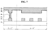
- a conductive film 44 is formed in the trench 28 and the via hole 26 .
- the conductive film 44 may be formed, for example, by electro plating and/or electroless plating.
- the formed conductive film 44 may be thick enough to bury the trench 28 and the via hole 26 as shown in FIG. 7 .
- the conductive film 44 may be made of various conductive materials and/or combinations thereof.
- the conductive film 44 includes copper (Cu).
- the upper damascene wiring line 46 may be formed by performing a CMP process on the conductive film 44 until the second interlayer insulating film 24 is exposed.
- FIGS. 8 to 16 An integrated circuit (semiconductor) memory device according to other embodiments of the present invention and a method of fabricating (forming) the same will now be described with reference to FIGS. 8 to 16 .
- the embodiments illustrated in FIGS. 8 to 16 may be used as a SRAM device.
- FIG. 8 is a circuit diagram illustrating a cell of an integrated circuit memory device according to some embodiments of the present invention.
- the memory device is a CMOS SRAM device.
- the cell of the memory device includes first and second access transistors Q 1 , Q 2 , first and second actuating transistors Q 3 , Q 4 , and first and second load transistors Q 5 , Q 6 .
- the sources of the first and second actuating transistors Q 3 , Q 4 are connected to a ground line V SS , and the sources of the first and second load transistors Q 5 , Q 6 are connected to a power line V DD .
- the first actuating transistor Q 3 shown as an NMOS transistor
- the first load transistor Q 5 shown as a PMOS transistor
- the second actuating transistor Q 4 shown as a NMOS transistor
- the second load transistor Q 6 shown as a PMOS transistor
- Output stages of the first and second inverters are connected to sources of the first access transistor Q 1 and the second access transistor Q 2 , respectively. Furthermore, input stages and output stages of the first and second inverters are alternately connected so as to constitute a latch circuit. Drains of the first and second access transistors Q 1 , Q 2 are connected to first and second bit lines BL, /BL, respectively.
- FIG. 9 is a layout view illustrating a memory device according to other embodiments of the invention.
- FIG. 10 is a cross sectional view illustrating the memory device of FIG. 9 taken along the lines III-III′ and IV-IV′ of FIG. 9 .
- first and second active regions 104 a , 104 b , 106 a , 106 b are defined by device isolation layer patterns 102 .
- the illustrated first active regions 104 a and 104 b correspond to an n-type impurity region and the second active regions 106 a and 106 b correspond to a p-type impurity region.
- FIG. 9 shows that first and second active regions 104 a , 104 b , 106 a , 106 b are defined by device isolation layer patterns 102 .
- the illustrated first active regions 104 a and 104 b correspond to an n-type impurity region and the second active regions 106 a and 106 b correspond to a p-type impurity region.
- the first and second active regions 104 a , 104 b , 106 a , 106 b are illustrated as symmetrical in the cell, and each of the first and second active regions 104 a , 104 b , 106 a , 106 b is divided into two regions by the device isolation layer patterns 102 .
- First and second gate electrodes 114 a , 114 b intersect the first and second active regions 104 a , 104 b , 106 a , 106 b on the semiconductor substrate 100 in which the first and second active regions 104 a , 104 b , 106 a , 106 b are defined by the device isolation layer patterns 102 . Furthermore, a third gate electrode 114 c intersects the first active regions 104 a , 104 b , which are divided into two parts, and extends in a direction substantially orthogonal to the first and second gate electrodes 114 a and 114 b .
- the first or second gate electrode 114 a and 114 b may protrude toward the other gate electrodes on the device isolation layer patterns 102 between the first and second active regions 104 a , 104 b , 106 a , and 106 b . Additionally, gate oxide films 112 are provided under the first to third gate electrodes 114 a , 114 b , and 114 c and gate spacers 116 are provided at both ends of the first to third gate electrodes.
- the first and second gate electrodes 114 a and 114 b on an end thereof extending over the first active regions 104 a and 104 b , form gates of the third and fourth actuating transistors (see Q 3 and Q 4 of FIG. 8 ), and the first and second gate electrodes 114 a and 114 b , on an end thereof extending over the second active regions 106 a and 106 b , form gates of the fifth and sixth load transistors (see Q 5 and Q 6 of FIG. 8 ). Furthermore, the third gate electrode 114 c , which intersects the first active regions 104 a and 104 b , forms gates of the first and second access transistors (see Q 1 and Q 2 of FIG. 8 ).
- first interlayer insulating layer 118 is provided on the semiconductor substrate 100 on which the gate electrodes 114 a , 114 b , and 114 c are formed.
- Contacts 119 extend through the first interlayer insulating layer 118 to connect to the gate electrodes 114 a , 114 b , and 114 c .
- lower wiring lines 122 which are connected to the contacts 119 , are formed on an upper portion/surface of the first interlayer insulating layer 118 .
- the lower wiring lines 122 include a first lower wiring line 122 a connected to the first gate electrode 114 a , a second lower wiring line 122 b connected to the second gate electrode 114 b and extending over the active regions 104 a , 106 a , and a third lower wiring line 122 c extending over the active regions 104 b , 106 b .
- the first to third lower wiring lines 122 a , 122 b , and 122 c extend generally parallel to each other (i.e., they do not cross).
- a second interlayer insulating layer 124 is provided on the first interlayer insulating layer 118 on which the lower wiring lines 122 are formed.
- An upper damascene wiring line 146 which is connected to ones of the lower wiring lines 122 , is provided in the second interlayer insulating layer 124 .
- the upper damascene wiring line 146 which extends across the first to third lower wiring lines 122 a , 122 b , and 122 c , as described previously, includes a region that protrudes laterally from a portion thereof that intersects (overlies) the lower wiring lines 122 .
- Via holes 126 which are connected to the lower wiring lines 122 , are formed under the protruded region.
- Opposite ends of the upper damascene wiring line 146 are shown with protruding region, and respective via holes 126 are connected to lower portion of the protruded regions, so that the first lower wiring line 122 a and the third lower wiring line 122 c under both ends of the upper damascene wiring line 146 are electrically connected to each other.
- the ends of the upper damascene wiring line 146 may protrude in a same direction or in an opposite direction to each other.
- the upper damascene wiring line 146 may be a metal wiring line made of a metal material, such as copper, and a diffusion barrier film (see 142 of FIG. 17 ) is shown formed between the upper damascene wiring line 146 made of the metal material and the second interlayer insulating film 124 to limit or even prevent the metal material from being diffused therebetween. Additionally, a seed layer may be interposed between the diffusion barrier film (see 142 of FIG. 17 ) and the upper damascene wiring line 146 .
- the upper damascene wiring line 146 extends generally in a straight linear pattern in the second interlayer insulating layer 124 to selectively connect the lower wiring lines 122 .
- first active regions and second active regions 104 a , 104 b , 106 a , and 106 b are defined by forming device isolation layer patterns 102 in the semiconductor substrate 100 .
- a trench may be formed by selectively etching the semiconductor substrate 100
- the device isolation layer patterns 102 may be formed by burying an insulating material filling the trench.
- the first active regions and the second active regions 104 a , 104 b , 106 a , and 106 b may be formed by selectively ion-injecting n-type and p-type impurity materials into the semiconductor substrate 100 on which the device isolation layer patterns 102 are formed.
- the first active regions 104 a and 104 b are formed with the n-type impurity material
- the second active regions 106 a and 106 b are formed with the p-type impurity material.
- the first active regions and the second active regions 104 a , 104 b , 106 a , and 106 b are shown positioned symmetrically, and divided into two parts, respectively.
- a first gate electrode to a third gate electrode 114 a , 114 b , and 114 c are formed on the semiconductor substrate 100 including the first active regions and the second active regions 104 a , 104 b , 106 a , and 106 b .
- a gate oxide film and a gate conductive film may be sequentially formed on the semiconductor substrate 100 in which the first active regions and the second active regions 104 a , 104 b , 106 a , and 106 b are formed.
- the first to third gate electrodes 114 a , 114 b , and 114 c may be formed by a photolithography process. As shown in FIG.
- the first gate electrode and the second gate electrode 114 a and 114 b may be formed so as to intersect the first active regions and the second active regions 104 a , 104 b , 106 a , and 106 b .
- the first gate electrode and the second gate electrode 114 a and 114 b may also be formed to extend on the device isolation layer patterns 102 between the first active regions and the second active regions 104 a , 104 b , 106 a , and 106 b so as to protrude laterally toward the each other.
- the third gate electrode 114 c is shown formed so as to intersect (overly) the first active regions 104 a and 104 b , which are divided into two parts.
- source/drain regions are formed by ion-implanting the impurity into the first active regions and the second active regions 104 a , 104 b , 106 a , and 106 b at both sides of the first to third gate electrodes 114 a , 114 b , and 114 c .
- Gate spacers 116 may be formed at side walls of the first to third gate electrodes 114 a , 114 b , and 114 c by depositing an insulating layer on an overall surface and performing an etch back process that leaves the gate spacers 116 on the side walls.
- the first interlayer insulating layer 118 is formed on the surface of a resultant product.
- Contact holes are formed to expose the top of the first active regions and the second active regions 104 a , 104 b , 106 a , and 106 b and the first to third gate electrodes 114 a , 114 b , and 114 c by, for example, etching a selected region of the first interlayer insulating layer 118 .
- contacts 119 are formed in the first interlayer insulating layer 118 , for example, by flattening or polishing until the first interlayer insulating layer 118 is exposed.
- the lower wiring lines 122 may be formed so as to be connected to the respective contacts 119 .
- the illustrated lower wiring lines 122 include a first lower wiring line 122 a connected to the first gate electrode 114 a , a second lower wiring line 122 b through which ones of the first active regions and the second active regions 104 a , 104 b , 106 a , and 106 b may be connected to the second gate electrode 114 b , and a third lower wiring line 122 c through which ones of the first and second active regions 104 a , 104 b 106 a , and 106 b may be connected to each other.
- the first to third lower wiring lines 122 a , 122 b , and 122 c may be formed in a selected direction so as to extend substantially parallel to one another (i.e., without crossing each other).
- a second interlayer insulating film 124 and a first antireflective film 132 may be sequentially formed on the first interlayer insulating film 118 on which the lower wiring lines 122 are formed.
- the second interlayer insulating film 124 may be formed of a silicon oxidation film, for example, such as PSG (PhosphoSilicate Glass), BPSG (BoroPhosphoSilicate Glass), USG (UndopedSilicate Glass), and/or PE-TEOS (Plasma Enhanced-TetraEthyOrthoSilicate) and/or a low dielectric film, which may be fluorine or carbon doped.
- the first antireflective film 132 may be formed of an organic material.
- a first photoresist pattern 134 is shown formed on the first antireflective film 132 and patterned so as to form a via hole 126 .
- the first lower wiring line and the third lower wiring line 122 a and 122 c are exposed by respective via hole(s) 126 , only one of which is shown in FIG. 15 .
- the first photoresist pattern 134 as an etching mask, a portion of the second interlayer insulating layer 124 and the first antireflective film 132 may be sequentially etched to form the via hole(s) 126 , which expose the first lower wiring line and the third lower wiring line 122 a and 122 c , respectively.
- the first photoresist pattern 134 and the first antireflective film 132 which remain on the second interlayer insulating layer 124 , are removed. Then, as shown in FIG. 16 , a sacrificial film 136 is formed on the second interlayer insulating layer 124 . The sacrificial film 136 as seen in FIG. 16 fills (buries) the via hole 126 .
- the sacrificial film 136 may be dry-etched at a dry etching rate which is similar to that of the second interlayer insulating layer 124 , and may be formed of a SOD (Spin On Deposition) film having a high wet etching selectivity with respect to the low dielectric interlayer insulating layers.
- SOD Spin On Deposition
- the SOD film typically has an excellent via hole burying characteristic and flattening characteristic, the SOD film is generally used as a burying material or a flattening (planarization) material.
- HSQ Hydrophilicity
- MSQ Metal Silses Quioxane
- SOP Spin On Polymer
- a second antireflective film 138 which may be an organic material, is formed on the sacrificial film 136 .
- a second photoresist pattern 139 is formed on the second antireflective film 138 and patterned so as to form the trench 128 .
- the second photoresist pattern 139 as an etching mask, a portion of the second antireflective film 138 , the sacrificial film 136 , and the second interlayer insulating layer 124 may be sequentially etched.
- the sacrificial film 136 and the second interlayer insulating layer 124 may be etched regardless of the etching selectivity.
- the trench 128 may be formed in the second interlayer insulating layer 124 .
- the trench 128 is connected to the via hole 126 .
- the trench 128 formed extending over and across the first to third lower wiring lines 122 a , 122 b , and 122 c is formed in the second interlayer insulating layer 124 in a second direction different from and extending across the first direction in which the first to third lower wiring lines 122 a , 122 b , and 122 c extend.
- the second interlayer insulating layer 124 as shown in FIG. 17 does not overlap with the via hole 126 which is formed at the lower portion thereof.
- the trench 128 includes an extension region that protrudes from the region which intersects (overlies) the first lower wiring line and the third lower wiring line 122 a and 122 c , and the via hole(s) 126 are formed therein.
- the trench 128 is formed so that the both ends of the trench 128 protrude in the same direction or in an opposite direction to each other to correspond with the position of the via hole(s) 126 .
- the trench 128 is connected to the via hole 126 in the protruded region. That is, the via hole 126 connected to the first lower wiring line 122 a and the third lower wiring line 122 c is connected to the trench 128 .
- the width of the trench 128 of the protruded region connected to the via hole 126 may be similar to that of the lower via hole 126 . Accordingly, during the etching process of forming the trench 128 , the phenomenon in which a corner of the via hole 126 formed at the lower portion collapses in the direction of the second lower wiring line 122 b positioned at one side may be limited or even prevented.
- the second photoresist pattern 139 and the second antireflective film 138 are removed.
- the sacrificial film 136 remaining in the upper portion of the second interlayer insulating layer 124 and within the via hole 126 is removed.
- the illustrated trench 128 may be formed in the second interlayer insulating layer 124 .
- a diffusion barrier film 142 and a seed layer may be deposited conformally along the trench 128 and the via hole 126 .
- the diffusion barrier film 142 may be formed of, for example, of a material selected from Ta, TaN, TaSiN, Ti, TiN, TiSiN, W, and WN, or a combination thereof.
- the seed layer may be a copper film, which may be deposited by a CVD process and/or a PVD process.
- a conductive film 144 is formed in the trench 128 and the via hole 126 , on which the diffusion barrier film 142 and the seed layer are formed, for example, by performing an electro plating and/or an electroless plating.
- the conductive film 144 may have a thickness sufficient to fill (bury) the trench 128 and the via hole 126 .
- the conductive film 144 may be formed of various conductive materials and combination thereof. In some embodiments, the conductive film 144 includes copper (Cu).
- an upper damascene wiring line 146 is shown, which may be formed by performing the CMP process until the second interlayer insulating layer 124 is exposed.
- the upper damascene wiring line 146 is shown formed so as to selectively connect the other lower wiring lines 122 .
- additional wiring lines may be formed while forming the upper damascene wiring line 146 , which other wiring lines may selectively connect lower wiring lines 122 other than the lower wiring lines 122 a , 122 b , 122 c , which additional wiring lines may be formed in a straight line without a protruding portion as seen in FIG. 9 .
- a semiconductor memory device includes an upper damascene wiring line having protruded regions protruded laterally above the lower wiring lines formed in the interlayer insulating layer so as to be vertical (extend across) to the lower wiring lines, and that is provided with a via connected to the lower wiring lines at the lower portion of the protruded regions. Accordingly, during the forming of the trench which is connected to the via hole, it may limit or even prevent the phenomenon by which the corner of the via hole collapses toward the lower wiring line positioned at one side.
- the upper damascene wiring line as above-described, it may be possible to obtain an improved process margin.
Landscapes
- Engineering & Computer Science (AREA)
- Power Engineering (AREA)
- Physics & Mathematics (AREA)
- Condensed Matter Physics & Semiconductors (AREA)
- General Physics & Mathematics (AREA)
- Computer Hardware Design (AREA)
- Microelectronics & Electronic Packaging (AREA)
- Manufacturing & Machinery (AREA)
- General Engineering & Computer Science (AREA)
- Internal Circuitry In Semiconductor Integrated Circuit Devices (AREA)
Applications Claiming Priority (3)
| Application Number | Priority Date | Filing Date | Title |
|---|---|---|---|
| KR2005-74448 | 2005-08-12 | ||
| KR1020050074448A KR100632467B1 (ko) | 2005-08-12 | 2005-08-12 | 반도체 메모리 소자 및 그 제조 방법 |
| KR10-2005-0074448 | 2005-08-12 |
Publications (2)
| Publication Number | Publication Date |
|---|---|
| US20070035028A1 US20070035028A1 (en) | 2007-02-15 |
| US7768128B2 true US7768128B2 (en) | 2010-08-03 |
Family
ID=37635502
Family Applications (1)
| Application Number | Title | Priority Date | Filing Date |
|---|---|---|---|
| US11/499,059 Expired - Fee Related US7768128B2 (en) | 2005-08-12 | 2006-08-04 | Semiconductor memory devices including a damascene wiring line |
Country Status (2)
| Country | Link |
|---|---|
| US (1) | US7768128B2 (ko) |
| KR (1) | KR100632467B1 (ko) |
Cited By (5)
| Publication number | Priority date | Publication date | Assignee | Title |
|---|---|---|---|---|
| US20090152728A1 (en) * | 2007-12-06 | 2009-06-18 | Rohm Co., Ltd. | Semiconductor apparatus |
| US20100093145A1 (en) * | 2005-10-07 | 2010-04-15 | Renesas Technology Corp. | Semiconductor device and manufacturing method thereof for reducing the area of the memory cell region |
| US8741722B2 (en) | 2011-05-31 | 2014-06-03 | International Business Machines Corporation | Formation of dividers between gate ends of field effect transistor devices |
| US9356121B2 (en) | 2012-02-27 | 2016-05-31 | International Business Machines Corporation | Divot-free planarization dielectric layer for replacement gate |
| TWI631561B (zh) * | 2014-07-21 | 2018-08-01 | 愛思開海力士有限公司 | 閂鎖電路及包含該閂鎖電路的半導體裝置 |
Families Citing this family (1)
| Publication number | Priority date | Publication date | Assignee | Title |
|---|---|---|---|---|
| JP5096669B2 (ja) * | 2005-07-06 | 2012-12-12 | ルネサスエレクトロニクス株式会社 | 半導体集積回路装置の製造方法 |
Citations (6)
| Publication number | Priority date | Publication date | Assignee | Title |
|---|---|---|---|---|
| US5166902A (en) * | 1991-03-18 | 1992-11-24 | United Technologies Corporation | SRAM memory cell |
| US6127263A (en) | 1998-07-10 | 2000-10-03 | Applied Materials, Inc. | Misalignment tolerant techniques for dual damascene fabrication |
| KR20020050469A (ko) | 2000-12-21 | 2002-06-27 | 박종섭 | 반도체 소자의 금속 콘택 형성방법 |
| US6437455B2 (en) * | 2000-01-14 | 2002-08-20 | Seiko Epson Corporation | Semiconductor device having gate-gate, drain-drain, and drain-gate connecting layers and method of fabricating the same |
| KR20040039593A (ko) | 2002-11-04 | 2004-05-12 | 주식회사 하이닉스반도체 | 반도체 소자의 듀얼 다마신 패턴 형성 방법 |
| US7446418B2 (en) * | 2002-07-31 | 2008-11-04 | Fujitsu Limited | Semiconductor device for preventing defective filling of interconnection and cracking of insulating film |
-
2005
- 2005-08-12 KR KR1020050074448A patent/KR100632467B1/ko not_active IP Right Cessation
-
2006
- 2006-08-04 US US11/499,059 patent/US7768128B2/en not_active Expired - Fee Related
Patent Citations (6)
| Publication number | Priority date | Publication date | Assignee | Title |
|---|---|---|---|---|
| US5166902A (en) * | 1991-03-18 | 1992-11-24 | United Technologies Corporation | SRAM memory cell |
| US6127263A (en) | 1998-07-10 | 2000-10-03 | Applied Materials, Inc. | Misalignment tolerant techniques for dual damascene fabrication |
| US6437455B2 (en) * | 2000-01-14 | 2002-08-20 | Seiko Epson Corporation | Semiconductor device having gate-gate, drain-drain, and drain-gate connecting layers and method of fabricating the same |
| KR20020050469A (ko) | 2000-12-21 | 2002-06-27 | 박종섭 | 반도체 소자의 금속 콘택 형성방법 |
| US7446418B2 (en) * | 2002-07-31 | 2008-11-04 | Fujitsu Limited | Semiconductor device for preventing defective filling of interconnection and cracking of insulating film |
| KR20040039593A (ko) | 2002-11-04 | 2004-05-12 | 주식회사 하이닉스반도체 | 반도체 소자의 듀얼 다마신 패턴 형성 방법 |
Cited By (12)
| Publication number | Priority date | Publication date | Assignee | Title |
|---|---|---|---|---|
| US20100093145A1 (en) * | 2005-10-07 | 2010-04-15 | Renesas Technology Corp. | Semiconductor device and manufacturing method thereof for reducing the area of the memory cell region |
| US8183114B2 (en) * | 2005-10-07 | 2012-05-22 | Renesas Electronics Corporation | Semiconductor device and manufacturing method thereof for reducing the area of the memory cell region |
| US20090152728A1 (en) * | 2007-12-06 | 2009-06-18 | Rohm Co., Ltd. | Semiconductor apparatus |
| US8026607B2 (en) * | 2007-12-06 | 2011-09-27 | Rohm Co., Ltd. | Semiconductor apparatus |
| US8791569B2 (en) | 2007-12-06 | 2014-07-29 | Rohm Co., Ltd. | Semiconductor apparatus |
| US9368431B2 (en) | 2007-12-06 | 2016-06-14 | Rohm Co., Ltd. | Semiconductor apparatus |
| US9659868B2 (en) | 2007-12-06 | 2017-05-23 | Rohm Co., Ltd. | Semiconductor apparatus |
| US10037939B2 (en) | 2007-12-06 | 2018-07-31 | Rohm Co., Ltd. | Semiconductor apparatus |
| US8741722B2 (en) | 2011-05-31 | 2014-06-03 | International Business Machines Corporation | Formation of dividers between gate ends of field effect transistor devices |
| US9356121B2 (en) | 2012-02-27 | 2016-05-31 | International Business Machines Corporation | Divot-free planarization dielectric layer for replacement gate |
| US9876091B2 (en) | 2012-02-27 | 2018-01-23 | International Business Machines Corporation | Divot-free planarization dielectric layer for replacement gate |
| TWI631561B (zh) * | 2014-07-21 | 2018-08-01 | 愛思開海力士有限公司 | 閂鎖電路及包含該閂鎖電路的半導體裝置 |
Also Published As
| Publication number | Publication date |
|---|---|
| KR100632467B1 (ko) | 2006-10-09 |
| US20070035028A1 (en) | 2007-02-15 |
Similar Documents
| Publication | Publication Date | Title |
|---|---|---|
| US9564433B2 (en) | Semiconductor device with improved contact structure and method of forming same | |
| TWI566380B (zh) | 具垂直元件的雙埠靜態隨機存取記憶體單元結構及其製造方法 | |
| US7786520B2 (en) | Embedded semiconductor device including planarization resistance patterns and method of manufacturing the same | |
| US6498089B2 (en) | Semiconductor integrated circuit device with moisture-proof ring and its manufacture method | |
| JP5388768B2 (ja) | ローカルインターコネクトを備えた半導体装置 | |
| US20040018725A1 (en) | Unitary interconnection structures integral with a dielectric layer and fabrication methods thereof | |
| KR20120041642A (ko) | 반도체 소자 | |
| KR102489216B1 (ko) | 상호 접속 구조체 및 그 형성 방법 | |
| US7768128B2 (en) | Semiconductor memory devices including a damascene wiring line | |
| CN111463215B (zh) | 存储器结构及其制造方法 | |
| US20230307423A1 (en) | Semiconductor device and method of fabricating the same | |
| TW202029339A (zh) | 積體電路結構及其形成方法 | |
| US7186617B2 (en) | Methods of forming integrated circuit devices having a resistor pattern and plug pattern that are made from a same material | |
| US20220359387A1 (en) | Structure and method of forming a semiconductor device with resistive elements | |
| US7928002B2 (en) | Method of forming wiring layer of semiconductor device | |
| TW202013471A (zh) | 形成半導體裝置的方法 | |
| KR100526870B1 (ko) | 반도체 소자에서의 국부 상호연결배선 형성방법 | |
| US11309244B2 (en) | Electrical fuse structure and method of formation | |
| US20080067692A1 (en) | Semiconductor devices having contact pad protection for reduced electrical failures and methods of fabricating the same | |
| US6776622B2 (en) | Conductive contact structure and process for producing the same | |
| US20230238323A1 (en) | Interconnect structure including vertically stacked power and ground lines | |
| US20230067527A1 (en) | Semiconductor structure having deep metal line and method for forming the semiconductor structure | |
| JP5687317B2 (ja) | 半導体装置の製造方法 | |
| KR20070006231A (ko) | 반도체 소자의 비트 라인 형성 방법 |
Legal Events
| Date | Code | Title | Description |
|---|---|---|---|
| AS | Assignment |
Owner name: SAMSUNG ELECTRONICS CO., LTD., KOREA, REPUBLIC OF Free format text: ASSIGNMENT OF ASSIGNORS INTEREST;ASSIGNORS:CHO, YOUNG-WOO;LEE, KYUNG-TAE;SHIN, HEON-JONG;AND OTHERS;SIGNING DATES FROM 20060712 TO 20060716;REEL/FRAME:018159/0729 Owner name: SAMSUNG ELECTRONICS CO., LTD., KOREA, REPUBLIC OF Free format text: ASSIGNMENT OF ASSIGNORS INTEREST;ASSIGNORS:CHO, YOUNG-WOO;LEE, KYUNG-TAE;SHIN, HEON-JONG;AND OTHERS;REEL/FRAME:018159/0729;SIGNING DATES FROM 20060712 TO 20060716 |
|
| FPAY | Fee payment |
Year of fee payment: 4 |
|
| FEPP | Fee payment procedure |
Free format text: MAINTENANCE FEE REMINDER MAILED (ORIGINAL EVENT CODE: REM.) |
|
| LAPS | Lapse for failure to pay maintenance fees |
Free format text: PATENT EXPIRED FOR FAILURE TO PAY MAINTENANCE FEES (ORIGINAL EVENT CODE: EXP.); ENTITY STATUS OF PATENT OWNER: LARGE ENTITY |
|
| STCH | Information on status: patent discontinuation |
Free format text: PATENT EXPIRED DUE TO NONPAYMENT OF MAINTENANCE FEES UNDER 37 CFR 1.362 |
|
| FP | Lapsed due to failure to pay maintenance fee |
Effective date: 20180803 |