US7719086B2 - Lateral insulated gate bipolar transistor having a retrograde doping profile in base region and method of manufacture thereof - Google Patents
Lateral insulated gate bipolar transistor having a retrograde doping profile in base region and method of manufacture thereof Download PDFInfo
- Publication number
- US7719086B2 US7719086B2 US11/943,614 US94361407A US7719086B2 US 7719086 B2 US7719086 B2 US 7719086B2 US 94361407 A US94361407 A US 94361407A US 7719086 B2 US7719086 B2 US 7719086B2
- Authority
- US
- United States
- Prior art keywords
- region
- base region
- type
- base
- conductivity type
- Prior art date
- Legal status (The legal status is an assumption and is not a legal conclusion. Google has not performed a legal analysis and makes no representation as to the accuracy of the status listed.)
- Active, expires
Links
Images


Classifications
-
- H—ELECTRICITY
- H10—SEMICONDUCTOR DEVICES; ELECTRIC SOLID-STATE DEVICES NOT OTHERWISE PROVIDED FOR
- H10D—INORGANIC ELECTRIC SEMICONDUCTOR DEVICES
- H10D12/00—Bipolar devices controlled by the field effect, e.g. insulated-gate bipolar transistors [IGBT]
- H10D12/01—Manufacture or treatment
-
- H—ELECTRICITY
- H10—SEMICONDUCTOR DEVICES; ELECTRIC SOLID-STATE DEVICES NOT OTHERWISE PROVIDED FOR
- H10D—INORGANIC ELECTRIC SEMICONDUCTOR DEVICES
- H10D12/00—Bipolar devices controlled by the field effect, e.g. insulated-gate bipolar transistors [IGBT]
- H10D12/411—Insulated-gate bipolar transistors [IGBT]
-
- H—ELECTRICITY
- H10—SEMICONDUCTOR DEVICES; ELECTRIC SOLID-STATE DEVICES NOT OTHERWISE PROVIDED FOR
- H10D—INORGANIC ELECTRIC SEMICONDUCTOR DEVICES
- H10D12/00—Bipolar devices controlled by the field effect, e.g. insulated-gate bipolar transistors [IGBT]
- H10D12/01—Manufacture or treatment
- H10D12/031—Manufacture or treatment of IGBTs
-
- H—ELECTRICITY
- H10—SEMICONDUCTOR DEVICES; ELECTRIC SOLID-STATE DEVICES NOT OTHERWISE PROVIDED FOR
- H10D—INORGANIC ELECTRIC SEMICONDUCTOR DEVICES
- H10D62/00—Semiconductor bodies, or regions thereof, of devices having potential barriers
- H10D62/10—Shapes, relative sizes or dispositions of the regions of the semiconductor bodies; Shapes of the semiconductor bodies
- H10D62/17—Semiconductor regions connected to electrodes not carrying current to be rectified, amplified or switched, e.g. channel regions
- H10D62/393—Body regions of DMOS transistors or IGBTs
Definitions
- the present invention mainly relates to an insulated gate bipolar transistor (hereafter abbreviated as “IGBT”)
- the current capability of the lateral IGBT at forward bias must be improved.
- the current capability of the lateral IGBT is measured on at least on-state voltage and characteristics of destroying devices, such as SOA (safe operating area) and ESD (electrostatic discharge).
- FIG. 9 shows a general lateral IGBT on a SOI substrate.
- An N-type semiconductor layer 3 is bonded on a supporting substrate 1 via a buried insulating film 2 .
- a P-type base region 4 and an N-type buffer region 8 are formed on the surface of the N-type semiconductor layer 3 .
- an N + -type emitter region 5 and a P + -type base contact diffusion region 10 are diffused on the surface of the N-type buffer region 8 .
- a P + -type collector region 9 is diffused.
- a gate electrode 7 extends above a field oxide film 11 via a gate insulating film 6 .
- an emitter electrode 12 is formed, and on the P + -type collector region 9 , a collector electrode 13 is formed on the P + -type collector region 9 .
- On-state voltage chiefly depends on the resistance component when the device is in the on-state.
- the channel resistance formed below the gate insulating film 6 is one of major resistance components, and the reduction thereof is important. Whereas, the control of latch up is important for SOA.
- the equivalent circuit of the lateral IGBT has a thyristor structure as shown in FIG. 11 .
- the thyristor causes latch-up, the thyristor cannot be controlled by gate voltage and a low-impedance state is produced bringing in breakdown.
- the condition of generating latch up is: ⁇ (NPN) + ⁇ (PNP) ⁇ 1 where ⁇ (NPN) and ⁇ (PNP) are the common base current gains of the parasitic NPN transistor and PNP transistor, respectively.
- a P + -type base contact diffusion region 10 of a high concentration is inserted under the N + -type emitter region 5 .
- a dedicated high-concentration diffusion layer having larger diffusion depth may be diffused from the surface instead of the P + -type base contact diffusion region 10 .
- the P + -type base contact diffusion region 10 and the dedicated high-concentration diffusion layer since channel resistance is increased when diffusion reaches under the gate electrode 7 , a sufficient margin is required in the distance L 1 to the gate electrode 7 shown in FIG. 10 .
- the base resistance becomes the serial resistance of the distance L 1 of a low concentration and the distance L 2 of a high concentration.
- the turn-on of the parasitic NPN transistor depends on the voltage drop in the distance L 1 having a higher resistance.
- the distance L 1 is easily varied by the widths of the gate electrode 7 and the P + -type base contact diffusion region 10 , and their misalignment.
- the lateral spread of diffusion is easily influenced by variation of heat treatment (drive-in temperature and time) then it's variation changes the distance L 1 .
- a high-concentration P-type region 14 is continuously added under a P-type base region 4 .
- a high-concentration P-type region 14 is formed under an emitter region 5 .
- the high-concentration P-type region 14 is formed by self-aligning to the gate electrode 7 so as not to affect the channel portion.
- the concentration of a P-type impurity is increased in the P-type base region under the gate electrode located in the lateral direction near the emitter end, and alternatively, the width of the P-type base region is expanded in the lateral direction.
- the width of the P-type base region under the gate electrode would rather be reduced as much as possible.
- all of the above-described conventional techniques have normal diffusion profiles, specifically Gaussian distribution wherein the surface concentration is highest. Therefore, if the entire impurity concentration is increased, the surface concentration is also increased.
- the increase of the surface concentration not only results in the increase of channel resistance, but also increases emitter resistance because the low concentration of N-type impurity in the emitter region under the sidewalls of the gate electrode might be affected. Therefore, the impurity concentration in the P-type base region cannot be set to be high. Consequently, it is difficult to reduce the width of the P-type base region under the gate electrode.
- a high-concentration P-type region 14 is present only under the emitter region 5 , and a low-concentration P-type region is present under the gate electrode 7 .
- a semiconductor device includes a supporting substrate; a semiconductor layer of a first conductivity type formed above a main surface of the supporting substrate via a buried insulating film; a first base region of a second conductivity type formed from the surface of the semiconductor layer; a second base region of the second conductivity type having a concentration lower than the surface concentration of the first base region, and including the first base region fully or partly; a buffer region of the first conductivity type formed from the surface of the semiconductor layer apart from the second base region in the lateral direction; an emitter region of the first conductivity type formed from the surface of the first base region; a collector region of the second conductivity type formed from the surface of the buffer region; a base contact diffusion region of the second conductivity type formed from the surface of the first base region or the second base region; a gate insulating film formed on the second base region at least from an end of the emitter region to an end of the second base region; a gate electrode formed on the gate insulating film; an emitter electrode connected on the emitter
- a semiconductor device includes a supporting substrate; a second base region composed of a semiconductor layer of a second conductivity type formed above a main surface of the supporting substrate via a buried insulating film; a first base region of a second conductivity type formed from the surface of the second base region; a well region of a first conductivity type formed in the semiconductor layer apart from the first base region in the lateral direction; a buffer region of the first conductivity type adjoining the well region; an emitter region of the first conductivity type formed from the surface of the first base region; a collector region of the second conductivity type formed from the surface of the buffer region; a base contact diffusion region of the second conductivity type formed in the first base region; a gate insulating film formed on the second base region at least from an end of the emitter region to an end of the well region; a gate electrode formed on the gate insulating film; an emitter electrode connected on the emitter region and the base contact diffusion region; and a collector electrode connected on the collector region; wherein the first
- a semiconductor device includes a semiconductor substrate having two main surfaces; a semiconductor layer of a first conductivity type adjoining to one of the main surfaces of the semiconductor substrate; a first base region of a second conductivity type formed from the surface of the semiconductor layer; a second base region of the second conductivity type having a concentration lower than the surface concentration of the first base region, and involving the first base region; a base contact diffusion region of the second conductivity type formed from the surface of the first base region or the second base region; an emitter region of the first conductivity type formed from the surface of the first base region; a collector region of the second conductivity type adjoining to the other main surface of the semiconductor substrate; a buffer layer of the first conductivity type inserted between the collector region and the semiconductor layer; a gate insulating film formed at least from an end of the emitter region to an end of the second base region; a gate electrode formed on the gate insulating film; an emitter electrode connected on the emitter region and the base contact diffusion region; and a collector electrode connected on the
- the base contact diffusion region of the second conductivity type is extended to under the emitter region.
- a method of the manufacture of a semiconductor device includes the steps of forming a first base region of a second conductivity type on the surface of a semiconductor layer; forming a second base region having a lower concentration and a larger diffusion depth than the first base region so as to include the first base region fully or partly; forming a buffer region of the second conductivity type in the semiconductor layer apart from the second base region; sequentially forming a gate insulating film and a gate electrode on the first base region and the second base region; forming an emitter region of a first conductivity type on the surface of the first base region; and forming a collector region of the first conductivity type on the surface of the buffer layer; wherein the first base region is formed before the step of forming the gate insulating film using the implantation of boron ions with accelerating energy within a range between 150 KeV and 200 KeV, and a dose within a range between 3 ⁇ 10 13 and 1 ⁇ 10 14 ions/cm 2 .
- the first base region and the gate electrode are disposed so that the end portions thereof overlap each other.
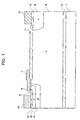
- FIG. 1 is a sectional view of a lateral IGBT, which is a first embodiment of the present invention
- FIG. 2 is a supplemental sectional view of the lateral IGBT, which is the first embodiment of the present invention
- FIG. 3 is a graph showing an impurity concentration profile in A-AA cross-section of the lateral IGBT shown in FIG. 2 ;
- FIG. 4 is a graph showing an impurity concentration profile in B-BB cross-section of the lateral IGBT shown in FIG. 2 ;
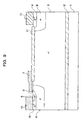
- FIG. 5 is a sectional view of a lateral IGBT, which is a second embodiment of the present invention.
- FIG. 6 is a sectional view of a vertical IGBT, which is a third embodiment of the present invention.
- FIG. 7 is a plan view of the lateral IGBT, which is the first embodiment of the present invention.
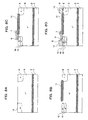
- FIG. 8A is a sectional view of a method of the manufacture of the lateral IGBT, which is the first embodiment of the present invention.
- FIG. 8B is a sectional view of a method of the manufacture of the lateral IGBT, which is the first embodiment of the present invention.
- FIG. 8C is a sectional view of a method of the manufacture of the lateral IGBT, which is the first embodiment of the present invention.
- FIG. 8D is a sectional view of a method of the manufacture of the lateral IGBT, which is the first embodiment of the present invention.
- FIG. 9 is a sectional view of a lateral IGBT
- FIG. 10 is a supplemental sectional view of a lateral IGBT
- FIG. 11 is an equivalent circuit schematic of a lateral IGBT
- FIG. 12 is a sectional view of a lateral IGBT of a first conventional example
- FIG. 13 is a sectional view of a lateral IGBT of a second conventional example.
- FIG. 14 is a graph showing the relationship between on-state breakdown voltage and dimensional ratio (w/d) of a lateral IGBT of the present invention.
- the first base region of an insulated gate bipolar transistor (IGBT) of the present invention has the following three characteristics:
- the first base region has a retrograde profile having the maximum (peak) of the concentration of an impurity of a second conductivity type under the emitter region of a first conductivity type, and the impurity concentration is gradually increased from the surface toward the peak.
- the first base region slightly extends from under the end of the gate electrode toward the collector region of the second conductivity type.
- the length in the lateral direction from the maximum point of impurity concentration under the end of the gate electrode is not smaller than the vertical length from the maximum point.
- the first base region is adjacent to or included in the region of the second conductivity type of a low impurity concentration.
- the P-type region of a low impurity concentration is equivalent to the second base region or a semiconductor layer.
- the off-state breakdown voltage can be increased.
- the first base region is formed near the surface, and the diffusion depth is not significantly large. Therefore, when the first base region is adjacent to the semiconductor layer of the first conductivity type, due to its curvature, increasing electric field lowers the off-state breakdown voltage.
- the present invention by adjoining the first base region with a region of a second conductivity type of a low impurity concentration that has a relatively large diffusion depth, the reduction of electric field could be obtained, then the off-state breakdown voltage is improved.
- an excellent device structure that is particularly effective for a lateral IGBT of high breakdown voltage, can lower on-state voltage and improve SOA at the same time, and can improve the current capability.
- the present invention also has effects when applied to a vertical IGBT.
- a vertical element although the collector region and the buffer region are formed on the back-face side of a substrate, the method for forming the base region is the same as the method described for the lateral IGBT.
- the first base region and the second base region having a retrograde profile must be formed before forming a polysilicon gate. Thereby, the first base region and the second base region can be formed under the gate electrode.
- boron ions are implanted by a relatively high accelerating energy within a range between 150 and 200 KeV. Thereafter, heat treatment called drive-in is performed to form a retrograde profile having a peak at a depth of about 0.5 ⁇ m from the surface.
- FIG. 1 shows a sectional view of a lateral IGBT according to the first embodiment of the present invention
- FIG. 7 shows a plan view thereof.
- a second P ⁇ -type base region 15 and an N-type buffer region 8 are diffused apart from each other.
- the second P ⁇ -type base region 15 is often shared with a P-type well region of a low voltage NMOS transistor or a P-type offset region of a high voltage PMOS transistor integrated in the same chip, and the surface impurity concentration is as relatively low as about 1 ⁇ 10 16 cm ⁇ 2 .
- a first P-type base region 16 is formed in the second P ⁇ -type base region 15 ; and further in the first P-type base region 16 , an N + -type emitter region 5 and a P + -type base contact diffusion region 10 are diffused.
- a gate electrode 7 is formed above the first P-type base region 16 and the second P ⁇ -type base region 15 via a gate insulating film 6 , and extends above a field oxide film 11 .
- an emitter electrode 12 is formed on the N + -type emitter region 5 and the P + -type base contact diffusion region 10 .
- a P + -type collector region 9 is formed on the N-type buffer region 8 , and a collector electrode 13 is further formed on the P + -type collector region 9 .
- the first P-type base region 16 is formed under the N + -type emitter region 5 .
- the P + -type collector region 9 has a shape having two corner portions and two straight portions; and the P + -type collector region 9 is surrounded by an N-type buffer layer 8 and an N-type semiconductor layer 3 .
- the N + -type emitter regions 5 are formed on the straight portions, and are not formed on the corner portions. Thereby, current crowding the corner portions is suppressed.
- FIG. 2 is a supplemental sectional view; and FIG. 3 is a graph showing an impurity concentration profile in the vertical direction in A-AA cross-section shown in FIG. 2 .
- the distance from the maximum point of impurity concentrations to the boundary point with the second base region 15 is represented by “d”.
- FIG. 4 shows an impurity concentration profile in the lateral direction in B-BB cross-section shown in FIG. 2 .
- the B-BB cross-section is a profile from under the gate electrode 7 toward the collector region 9 side in the peak of the A-AA cross-section.
- the boundary between the first P-type base region 16 and the second P ⁇ -type base region 15 is the place where the gradient of impurity concentration is changed, and the distance from under the end of the gate electrode 7 is represented by “w”.
- the PN junction depth of the N + -type emitter region 5 and the first P-type base region 16 is about 0.1 ⁇ m.
- the peak of the concentration of the P-type impurity is about 1 ⁇ 10 18 cm ⁇ 3 , and is located at a depth of 0.5 ⁇ m from the surface and under the N + -type emitter region 5 .
- the boundary between the first P-type base region 16 and the second P-type base region 15 is located at about 1.4 ⁇ m from the surface where the concentration gradient is changed.
- the concentration of the P-type impurity lowers relatively slowly, and the surface concentration becomes about 2 ⁇ 10 17 cm ⁇ 3 .
- Such a retrograde doping profile can be easily formed by ion implantation of boron at a dose of 6.5 ⁇ 10 13 ions/cm 2 and an accelerating energy of about 180 KeV, and appropriate heat treatment of diffusion called drive-in.
- the surface concentration of the second P ⁇ -type base region 15 is about 1 ⁇ 10 16 cm 3 .
- the first P-type base region 16 is extended to increase the concentration of the P-type impurity in the second P ⁇ -type base region 15 under the gate electrode 7 located in the lateral direction from the end of an emitter region 5 .
- FIG. 14 shows the relationship between on-state breakdown voltage, on-state voltage and “w/d”. We consider on-state breakdown voltage rather than current. On the other hand, “w/d” on the abscissa is set because it could indirectly show the ratio of the quantities of the impurity in the vertical direction and the lateral direction.
- the P-type diffusion region is formed before the polysilicon gate electrode, the P-type diffusion region can be extended in an optimal length under the gate electrode, and “1 ⁇ w/d ⁇ 2” can be easily realized.
- the first P-type base region 16 is formed under the base contact diffusion region 10
- the second P ⁇ -type base region 15 is formed under the first P-type base region 16
- the first P-type base region 16 may be not formed under the base contact diffusion region 10 , if the base contact diffusion region 10 is formed from the surface of the second P ⁇ -type base region 15 .
- FIG. 5 shows a lateral IGBT according to the second embodiment of the present invention, wherein only the following aspects are different from the first embodiment.
- the lateral IGBT shown in FIG. 5 has a device structure using an SOI substrate on which a P-type semiconductor layer 17 is formed, and the P-type semiconductor layer 17 reaches a buried insulating film 2 .
- a first P-type base region 16 as a first base region an N + -type emitter region 5 and a P + -type base contact diffusion region 10 are diffused.
- the first P-type base region 16 is extended to a part under a gate electrode 7 while having a vertical concentration profile of a P-type impurity that increases from the surface of the P-type semiconductor layer 17 and becomes highest under the N + -type emitter region 5 .
- the lateral length w from the maximum point of the impurity concentration located under an end portion of the gate electrode 7 is not smaller than vertical length d from the above-described maximum point, and the P-type semiconductor layer 17 from immediately under the first P-type base region 16 to the buried insulating film 2 has a concentration at least ten times lower than the surface concentration of the first P-type base region 4 .
- the impurity concentration of the P-type semiconductor layer 17 is 3 ⁇ 10 +15 cm ⁇ 3 , and is suppressed to at least ten times lower than the surface concentration of the first P-type base region 16 of 2 ⁇ 10 +17 cm ⁇ 3 .
- FIG. 6 shows a sectional view of a vertical IGBT according to the third embodiment of the present invention.
- a P-type collector region 9 is formed on the back face of a substrate 20 , and an N-type buffer region 8 is formed on the P-type collector region 9 .
- An N-type semiconductor layer 3 is formed thereon.
- Second P ⁇ -type base regions 15 are spaced between each other near the surface, and on the surface of the second P ⁇ -type base region 15 , a first P-type base region 16 is formed.
- an N + -type emitter region 5 and a P + -type base contact diffusion region 10 are formed on the surface of the first P-type base region 16 , and an emitter electrode 12 is formed thereon.
- a gate electrode 7 is formed from an end of the N + -type emitter region 5 via the gate insulating film 6 .
- the first P-type base region 16 has a retrograde profile having the peak under the N + -type emitter region 5 , and is extended under the gate electrode.
- the first P-type base region 16 is extended to a part under the gate electrode 7 while having a vertical concentration profile of a P-type impurity that increases from the surface of the N-type semiconductor layer 3 and becomes highest under the emitter region 5 .
- the lateral length w from the maximum point of the impurity concentration located under an end portion of the gate electrode 7 is not smaller than the vertical length d from the above-described maximum point.
- the first P-type base region 16 is formed under the base contact diffusion region 10
- the second P ⁇ -type base region 15 is formed under the first P-type base region 16
- a configuration wherein the first P-type base region 16 is not formed under the base contact diffusion region 10 can also be formed, and in this case, the base contact diffusion region 10 is formed from the surface of the second P ⁇ -type base region 15 as the second base region.
- FIG. 8 shows a method of the manufacture of an IGBT according to the first embodiment of the present invention.
- a second P ⁇ -type base region 15 and an N-type buffer region 8 are formed on the surface of an N-type semiconductor layer 3 using ion implantation and heat treatment called drive-in.
- a LOCOS film 11 is formed, and a first P-type base region 16 is formed on the surface of the second P ⁇ -type base region 15 using boron ion implantation.
- the accelerating energy is, for example, 180 KeV, and the dose is 6.5 ⁇ 10 13 ions/cm 2 .
- a gate electrode 7 of polysilicon is formed so that the end portion thereof overlaps the first P-type base region 16 .
- an N + -type emitter region 5 , a P + -type collector region 9 , and a P + -type base contact diffusion region 10 are formed by ion implantation. Furthermore, an emitter electrode 12 and a collector electrode 13 are formed.
- the P + -type base contact diffusion region 10 may be extended to under the emitter region 5 to further lower the resistance of the base region. Thereby, the turn-on of the parasitic NPN transistor can be further suppressed.
- the first P-type base region 16 can be formed before the formation of the gate insulating film 6 by implanting boron ions using accelerating energy within a range between 150 KeV and 200 KeV and a dose within a range between 3 ⁇ 10 13 and 1 ⁇ 10 14 ions/cm 2 .
- the first conductivity type is N-type and the second conductivity type is P-type
- the first conductivity type can also be P-type
- the second conductivity type can also be N-type
Landscapes
- Insulated Gate Type Field-Effect Transistor (AREA)
- Thin Film Transistor (AREA)
Priority Applications (3)
| Application Number | Priority Date | Filing Date | Title |
|---|---|---|---|
| US12/662,680 US7944022B2 (en) | 2006-12-11 | 2010-04-28 | Lateral insulated gate bipolar transistor having a retrograde doping profile in base region and method of manufacture thereof |
| US12/963,665 US8093131B2 (en) | 2006-12-11 | 2010-12-09 | Lateral insulated gate bipolar transistor having a retrograde doping profile in base region and method of manufacture thereof |
| US13/064,430 US8304858B2 (en) | 2006-12-11 | 2011-03-24 | Lateral insulated gate bipolar transistor having a retrograde doping profile in base region and method of manufacture thereof |
Applications Claiming Priority (2)
| Application Number | Priority Date | Filing Date | Title |
|---|---|---|---|
| JP2006-332718 | 2006-12-11 | ||
| JP2006332718A JP5261927B2 (ja) | 2006-12-11 | 2006-12-11 | 半導体装置 |
Related Child Applications (1)
| Application Number | Title | Priority Date | Filing Date |
|---|---|---|---|
| US12/662,680 Division US7944022B2 (en) | 2006-12-11 | 2010-04-28 | Lateral insulated gate bipolar transistor having a retrograde doping profile in base region and method of manufacture thereof |
Publications (2)
| Publication Number | Publication Date |
|---|---|
| US20080135972A1 US20080135972A1 (en) | 2008-06-12 |
| US7719086B2 true US7719086B2 (en) | 2010-05-18 |
Family
ID=39496984
Family Applications (4)
| Application Number | Title | Priority Date | Filing Date |
|---|---|---|---|
| US11/943,614 Active 2028-01-31 US7719086B2 (en) | 2006-12-11 | 2007-11-21 | Lateral insulated gate bipolar transistor having a retrograde doping profile in base region and method of manufacture thereof |
| US12/662,680 Active US7944022B2 (en) | 2006-12-11 | 2010-04-28 | Lateral insulated gate bipolar transistor having a retrograde doping profile in base region and method of manufacture thereof |
| US12/963,665 Expired - Fee Related US8093131B2 (en) | 2006-12-11 | 2010-12-09 | Lateral insulated gate bipolar transistor having a retrograde doping profile in base region and method of manufacture thereof |
| US13/064,430 Expired - Fee Related US8304858B2 (en) | 2006-12-11 | 2011-03-24 | Lateral insulated gate bipolar transistor having a retrograde doping profile in base region and method of manufacture thereof |
Family Applications After (3)
| Application Number | Title | Priority Date | Filing Date |
|---|---|---|---|
| US12/662,680 Active US7944022B2 (en) | 2006-12-11 | 2010-04-28 | Lateral insulated gate bipolar transistor having a retrograde doping profile in base region and method of manufacture thereof |
| US12/963,665 Expired - Fee Related US8093131B2 (en) | 2006-12-11 | 2010-12-09 | Lateral insulated gate bipolar transistor having a retrograde doping profile in base region and method of manufacture thereof |
| US13/064,430 Expired - Fee Related US8304858B2 (en) | 2006-12-11 | 2011-03-24 | Lateral insulated gate bipolar transistor having a retrograde doping profile in base region and method of manufacture thereof |
Country Status (2)
| Country | Link |
|---|---|
| US (4) | US7719086B2 (enExample) |
| JP (1) | JP5261927B2 (enExample) |
Cited By (6)
| Publication number | Priority date | Publication date | Assignee | Title |
|---|---|---|---|---|
| US20090194785A1 (en) * | 2008-01-11 | 2009-08-06 | Fuji Electric Device Technology Co., Ltd. | Semiconductor device and manufacturing method thereof |
| US20100219448A1 (en) * | 2009-03-02 | 2010-09-02 | Hitachi, Ltd. | Semiconductor device and semiconductor integrated circuit device for driving plasma display using the semiconductor device |
| US20100327315A1 (en) * | 2009-06-30 | 2010-12-30 | Shinji Shirakawa | Semiconductor device, semiconductor integrated circuit device for use of driving plasma display with using same, and plasma display apparatus |
| US20110169046A1 (en) * | 2006-12-11 | 2011-07-14 | Panasonic Corporation | Lateral insulated gate bipolar transistor having a retrograde doping profile in base region and method of manufacture thereof |
| US9029869B2 (en) | 2010-09-06 | 2015-05-12 | Kabushiki Kaisha Toshiba | Semiconductor device |
| US10756172B2 (en) * | 2017-07-14 | 2020-08-25 | Panasonic Semiconductor Solutions Co., Ltd. | Semiconductor device |
Families Citing this family (19)
| Publication number | Priority date | Publication date | Assignee | Title |
|---|---|---|---|---|
| TWI387106B (zh) * | 2008-10-16 | 2013-02-21 | Vanguard Int Semiconduct Corp | 閘極絕緣雙接面電晶體(igbt)靜電放電防護元件 |
| JP2010165978A (ja) * | 2009-01-19 | 2010-07-29 | Panasonic Corp | 半導体装置およびその製造方法 |
| US8049307B2 (en) * | 2009-01-23 | 2011-11-01 | Vanguard International Semiconductor Corporation | Insulated gate bipolar transistor (IGBT) electrostatic discharge (ESD) protection devices |
| JP2012099517A (ja) * | 2010-10-29 | 2012-05-24 | Sony Corp | 半導体装置及び半導体装置の製造方法 |
| CN102856193B (zh) * | 2011-06-27 | 2015-05-13 | 中国科学院微电子研究所 | Igbt器件及其制作方法 |
| CN102856192B (zh) * | 2011-06-27 | 2015-05-13 | 中国科学院微电子研究所 | Igbt器件及其制作方法 |
| CN103650147B (zh) | 2011-07-05 | 2016-07-06 | 三菱电机株式会社 | 半导体装置 |
| US8581339B2 (en) * | 2011-08-08 | 2013-11-12 | Macronix International Co., Ltd. | Structure of NPN-BJT for improving punch through between collector and emitter |
| JP2013182905A (ja) * | 2012-02-29 | 2013-09-12 | Toshiba Corp | 半導体装置 |
| WO2014033991A1 (ja) * | 2012-08-30 | 2014-03-06 | パナソニック株式会社 | 半導体装置 |
| CN104347397B (zh) | 2013-07-23 | 2018-02-06 | 无锡华润上华科技有限公司 | 注入增强型绝缘栅双极型晶体管的制造方法 |
| JP2015026751A (ja) * | 2013-07-29 | 2015-02-05 | 株式会社日立製作所 | 横型バイポーラトランジスタおよびその製造方法 |
| CN103633087B (zh) * | 2013-12-19 | 2016-08-17 | 电子科技大学 | 一种具有esd保护功能的强抗闩锁可控ligbt器件 |
| US9960269B2 (en) * | 2016-02-02 | 2018-05-01 | Renesas Electronics Corporation | Semiconductor device and method of manufacturing the same |
| CN108242394A (zh) * | 2016-12-27 | 2018-07-03 | 全球能源互联网研究院 | 一种碳化硅mos栅控功率器件及其制备方法 |
| CN107919391B (zh) * | 2017-11-16 | 2020-07-03 | 重庆邮电大学 | 一种具有槽型氧化层和垂直缓冲层的rc-ligbt |
| CN108321195B (zh) * | 2018-02-05 | 2020-05-22 | 电子科技大学 | 一种具有阳极夹断槽的短路阳极soi ligbt |
| CN114175270A (zh) * | 2020-02-18 | 2022-03-11 | 富士电机株式会社 | 半导体装置 |
| CN111682062A (zh) * | 2020-06-24 | 2020-09-18 | 全球能源互联网研究院有限公司 | 一种igbt器件的背面结构及其制备方法、igbt器件 |
Citations (3)
| Publication number | Priority date | Publication date | Assignee | Title |
|---|---|---|---|---|
| JPH10242456A (ja) | 1997-02-28 | 1998-09-11 | Toshiba Corp | 横型絶縁ゲートバイポーラトランジスタ |
| JP2002270844A (ja) | 2001-03-07 | 2002-09-20 | Toshiba Corp | 半導体装置及びその製造方法 |
| US20060118902A1 (en) * | 2004-12-06 | 2006-06-08 | Matsushita Electric Industrial Co., Ltd. | Lateral semiconductor device and method for producing the same |
Family Cites Families (6)
| Publication number | Priority date | Publication date | Assignee | Title |
|---|---|---|---|---|
| JPH08130312A (ja) | 1994-09-08 | 1996-05-21 | Fuji Electric Co Ltd | 横型半導体装置およびその使用方法 |
| US5801420A (en) * | 1994-09-08 | 1998-09-01 | Fuji Electric Co. Ltd. | Lateral semiconductor arrangement for power ICS |
| JPH10150193A (ja) * | 1996-09-17 | 1998-06-02 | Toshiba Corp | 高耐圧半導体装置 |
| JP3473460B2 (ja) * | 1998-11-20 | 2003-12-02 | 富士電機株式会社 | 横型半導体装置 |
| JP4354876B2 (ja) * | 2004-06-10 | 2009-10-28 | パナソニック株式会社 | 半導体装置 |
| JP5261927B2 (ja) * | 2006-12-11 | 2013-08-14 | パナソニック株式会社 | 半導体装置 |
-
2006
- 2006-12-11 JP JP2006332718A patent/JP5261927B2/ja not_active Expired - Fee Related
-
2007
- 2007-11-21 US US11/943,614 patent/US7719086B2/en active Active
-
2010
- 2010-04-28 US US12/662,680 patent/US7944022B2/en active Active
- 2010-12-09 US US12/963,665 patent/US8093131B2/en not_active Expired - Fee Related
-
2011
- 2011-03-24 US US13/064,430 patent/US8304858B2/en not_active Expired - Fee Related
Patent Citations (3)
| Publication number | Priority date | Publication date | Assignee | Title |
|---|---|---|---|---|
| JPH10242456A (ja) | 1997-02-28 | 1998-09-11 | Toshiba Corp | 横型絶縁ゲートバイポーラトランジスタ |
| JP2002270844A (ja) | 2001-03-07 | 2002-09-20 | Toshiba Corp | 半導体装置及びその製造方法 |
| US20060118902A1 (en) * | 2004-12-06 | 2006-06-08 | Matsushita Electric Industrial Co., Ltd. | Lateral semiconductor device and method for producing the same |
Cited By (10)
| Publication number | Priority date | Publication date | Assignee | Title |
|---|---|---|---|---|
| US20110169046A1 (en) * | 2006-12-11 | 2011-07-14 | Panasonic Corporation | Lateral insulated gate bipolar transistor having a retrograde doping profile in base region and method of manufacture thereof |
| US8304858B2 (en) * | 2006-12-11 | 2012-11-06 | Panasonic Corporation | Lateral insulated gate bipolar transistor having a retrograde doping profile in base region and method of manufacture thereof |
| US20090194785A1 (en) * | 2008-01-11 | 2009-08-06 | Fuji Electric Device Technology Co., Ltd. | Semiconductor device and manufacturing method thereof |
| US7999317B2 (en) * | 2008-01-11 | 2011-08-16 | Fuji Electric Systems Co., Ltd. | Semiconductor device and manufacturing method thereof |
| US20100219448A1 (en) * | 2009-03-02 | 2010-09-02 | Hitachi, Ltd. | Semiconductor device and semiconductor integrated circuit device for driving plasma display using the semiconductor device |
| US8384124B2 (en) * | 2009-03-02 | 2013-02-26 | Hitachi, Ltd. | Semiconductor device and semiconductor integrated circuit device for driving plasma display using the semiconductor device |
| US20100327315A1 (en) * | 2009-06-30 | 2010-12-30 | Shinji Shirakawa | Semiconductor device, semiconductor integrated circuit device for use of driving plasma display with using same, and plasma display apparatus |
| US8487343B2 (en) * | 2009-06-30 | 2013-07-16 | Hitachi, Ltd. | Semiconductor device, semiconductor integrated circuit device for use of driving plasma display with using same, and plasma display apparatus |
| US9029869B2 (en) | 2010-09-06 | 2015-05-12 | Kabushiki Kaisha Toshiba | Semiconductor device |
| US10756172B2 (en) * | 2017-07-14 | 2020-08-25 | Panasonic Semiconductor Solutions Co., Ltd. | Semiconductor device |
Also Published As
| Publication number | Publication date |
|---|---|
| US8304858B2 (en) | 2012-11-06 |
| US8093131B2 (en) | 2012-01-10 |
| US20100213509A1 (en) | 2010-08-26 |
| US20080135972A1 (en) | 2008-06-12 |
| JP5261927B2 (ja) | 2013-08-14 |
| US7944022B2 (en) | 2011-05-17 |
| US20110169046A1 (en) | 2011-07-14 |
| US20110081751A1 (en) | 2011-04-07 |
| JP2008147415A (ja) | 2008-06-26 |
Similar Documents
| Publication | Publication Date | Title |
|---|---|---|
| US7944022B2 (en) | Lateral insulated gate bipolar transistor having a retrograde doping profile in base region and method of manufacture thereof | |
| US5514608A (en) | Method of making lightly-doped drain DMOS with improved breakdown characteristics | |
| KR100277611B1 (ko) | 접속주입부를사용한반도체장치및그제조방법 | |
| US9698246B1 (en) | LDMOS device with graded body doping | |
| US5218228A (en) | High voltage MOS transistors with reduced parasitic current gain | |
| US7238987B2 (en) | Lateral semiconductor device and method for producing the same | |
| US20020125542A1 (en) | Semiconductor device having insulated gate bipolar transistor with dielectric isolation structure and method of manufacturing the same | |
| TWI388011B (zh) | 半導體裝置及其形成方法 | |
| US7999285B2 (en) | Insulated gate bipolar transistor and method for manufacturing the same | |
| US9324861B2 (en) | Semiconductor device | |
| JP2011243919A (ja) | 半導体装置およびその製造方法 | |
| CN100565886C (zh) | 对衬底电压较不敏感的soi器件 | |
| US6472693B1 (en) | Semiconductor device and method of manufacturing the same | |
| US8829571B2 (en) | Punch-through semiconductor device and method for producing same | |
| JP3369862B2 (ja) | 半導体装置の製造方法 | |
| JP2008147318A (ja) | 高耐圧半導体装置及びその製造方法 | |
| US11756992B1 (en) | Semiconductor device with increased isolation breakdown voltage | |
| JP2006310770A (ja) | 高耐圧半導体装置及びその製造方法 | |
| JPH098294A (ja) | 絶縁ゲート型半導体装置およびその製造方法 |
Legal Events
| Date | Code | Title | Description |
|---|---|---|---|
| AS | Assignment |
Owner name: MATSUSHITA ELECTRIC INDUSTRIAL CO., LTD., JAPAN Free format text: ASSIGNMENT OF ASSIGNORS INTEREST;ASSIGNORS:IKUTA, TERUHISA;SATO, YOSHINOBU;REEL/FRAME:020705/0616;SIGNING DATES FROM 20070801 TO 20070802 Owner name: MATSUSHITA ELECTRIC INDUSTRIAL CO., LTD.,JAPAN Free format text: ASSIGNMENT OF ASSIGNORS INTEREST;ASSIGNORS:IKUTA, TERUHISA;SATO, YOSHINOBU;SIGNING DATES FROM 20070801 TO 20070802;REEL/FRAME:020705/0616 |
|
| AS | Assignment |
Owner name: PANASONIC CORPORATION, JAPAN Free format text: CHANGE OF NAME;ASSIGNOR:MATSUSHITA ELECTRIC INDUSTRIAL CO., LTD.;REEL/FRAME:021897/0516 Effective date: 20081001 Owner name: PANASONIC CORPORATION,JAPAN Free format text: CHANGE OF NAME;ASSIGNOR:MATSUSHITA ELECTRIC INDUSTRIAL CO., LTD.;REEL/FRAME:021897/0516 Effective date: 20081001 |
|
| FEPP | Fee payment procedure |
Free format text: PAYOR NUMBER ASSIGNED (ORIGINAL EVENT CODE: ASPN); ENTITY STATUS OF PATENT OWNER: LARGE ENTITY |
|
| STCF | Information on status: patent grant |
Free format text: PATENTED CASE |
|
| FPAY | Fee payment |
Year of fee payment: 4 |
|
| AS | Assignment |
Owner name: PANNOVA SEMIC, LLC, CALIFORNIA Free format text: ASSIGNMENT OF ASSIGNORS INTEREST;ASSIGNOR:PANASONIC CORPORATION;REEL/FRAME:036065/0273 Effective date: 20141226 |
|
| FEPP | Fee payment procedure |
Free format text: PAYER NUMBER DE-ASSIGNED (ORIGINAL EVENT CODE: RMPN); ENTITY STATUS OF PATENT OWNER: LARGE ENTITY Free format text: PAYOR NUMBER ASSIGNED (ORIGINAL EVENT CODE: ASPN); ENTITY STATUS OF PATENT OWNER: LARGE ENTITY |
|
| MAFP | Maintenance fee payment |
Free format text: PAYMENT OF MAINTENANCE FEE, 8TH YEAR, LARGE ENTITY (ORIGINAL EVENT CODE: M1552) Year of fee payment: 8 |
|
| MAFP | Maintenance fee payment |
Free format text: PAYMENT OF MAINTENANCE FEE, 12TH YEAR, LARGE ENTITY (ORIGINAL EVENT CODE: M1553); ENTITY STATUS OF PATENT OWNER: LARGE ENTITY Year of fee payment: 12 |