US7718734B2 - Organic semiconducting materials - Google Patents
Organic semiconducting materials Download PDFInfo
- Publication number
- US7718734B2 US7718734B2 US10/539,745 US53974503A US7718734B2 US 7718734 B2 US7718734 B2 US 7718734B2 US 53974503 A US53974503 A US 53974503A US 7718734 B2 US7718734 B2 US 7718734B2
- Authority
- US
- United States
- Prior art keywords
- molecular weight
- composition
- semiconducting
- compound
- coating
- Prior art date
- Legal status (The legal status is an assumption and is not a legal conclusion. Google has not performed a legal analysis and makes no representation as to the accuracy of the status listed.)
- Expired - Lifetime, expires
Links
- 0 *C1=CC=C2C(=C1)C([1*])([2*])C1=C2C=CC(*)=C1 Chemical compound *C1=CC=C2C(=C1)C([1*])([2*])C1=C2C=CC(*)=C1 0.000 description 9
- UUEDLRZNPFAXCN-UHFFFAOYSA-N C.C.CCN([Ar])CC.[Ar].[Ar] Chemical compound C.C.CCN([Ar])CC.[Ar].[Ar] UUEDLRZNPFAXCN-UHFFFAOYSA-N 0.000 description 2
- OGGKVJMNFFSDEV-UHFFFAOYSA-N CC1=CC(N(C2=CC=CC=C2)C2=CC=C(C3=CC=C(N(C4=CC=CC=C4)C4=CC=CC(C)=C4)C=C3)C=C2)=CC=C1 Chemical compound CC1=CC(N(C2=CC=CC=C2)C2=CC=C(C3=CC=C(N(C4=CC=CC=C4)C4=CC=CC(C)=C4)C=C3)C=C2)=CC=C1 OGGKVJMNFFSDEV-UHFFFAOYSA-N 0.000 description 2
- BYUPOQAUOOGCEQ-UHFFFAOYSA-N CC1=CC=C(N(C2=CC=CC3=CC=CC=C32)C2=CC=CC3=CC=CC=C32)C=C1 Chemical compound CC1=CC=C(N(C2=CC=CC3=CC=CC=C32)C2=CC=CC3=CC=CC=C32)C=C1 BYUPOQAUOOGCEQ-UHFFFAOYSA-N 0.000 description 2
- MBIBROLQSPDFOS-UHFFFAOYSA-N CC1=CC=C(N(C2=CC=CC=C2)C2=CC=C(C3=CC=C(N(C4=CC=CC=C4)C4=C(C)C=C(C)C=C4)C=C3)C=C2)C(C)=C1 Chemical compound CC1=CC=C(N(C2=CC=CC=C2)C2=CC=C(C3=CC=C(N(C4=CC=CC=C4)C4=C(C)C=C(C)C=C4)C=C3)C=C2)C(C)=C1 MBIBROLQSPDFOS-UHFFFAOYSA-N 0.000 description 2
- UNZWWPCQEYRCMU-UHFFFAOYSA-N CC1=CC=C(N(C2=CC=CC=C2)C2=CC=C(C3=CC=C(N(C4=CC=CC=C4)C4=CC=C(C)C=C4)C=C3)C=C2)C=C1 Chemical compound CC1=CC=C(N(C2=CC=CC=C2)C2=CC=C(C3=CC=C(N(C4=CC=CC=C4)C4=CC=C(C)C=C4)C=C3)C=C2)C=C1 UNZWWPCQEYRCMU-UHFFFAOYSA-N 0.000 description 2
- BLFVVZKSHYCRDR-UHFFFAOYSA-N C1=CC=C(N(C2=CC=C(C3=CC=C(N(C4=CC=CC=C4)C4=CC5=CC=CC=C5C=C4)C=C3)C=C2)C2=CC3=CC=CC=C3C=C2)C=C1 Chemical compound C1=CC=C(N(C2=CC=C(C3=CC=C(N(C4=CC=CC=C4)C4=CC5=CC=CC=C5C=C4)C=C3)C=C2)C2=CC3=CC=CC=C3C=C2)C=C1 BLFVVZKSHYCRDR-UHFFFAOYSA-N 0.000 description 1
- GVHNYXVWQNZEGS-UHFFFAOYSA-N C1=CC=C(N(C2=CC=CC3=CC=CC=C32)C2=CC=CC3=CC=CC=C32)C=C1 Chemical compound C1=CC=C(N(C2=CC=CC3=CC=CC=C32)C2=CC=CC3=CC=CC=C32)C=C1 GVHNYXVWQNZEGS-UHFFFAOYSA-N 0.000 description 1
- KNWWWMGCICBSSM-UHFFFAOYSA-N C1=CC=C(N(C2=CC=CC=C2)C2=CC=C(C3=CC=C(C4=CC=C(N(C5=CC=CC=C5)C5=CC=CC=C5)C=C4)C=C3)C=C2)C=C1 Chemical compound C1=CC=C(N(C2=CC=CC=C2)C2=CC=C(C3=CC=C(C4=CC=C(N(C5=CC=CC=C5)C5=CC=CC=C5)C=C4)C=C3)C=C2)C=C1 KNWWWMGCICBSSM-UHFFFAOYSA-N 0.000 description 1
- DCZNSJVFOQPSRV-UHFFFAOYSA-N C1=CC=C(N(C2=CC=CC=C2)C2=CC=C(C3=CC=C(N(C4=CC=CC=C4)C4=CC=CC=C4)C=C3)C=C2)C=C1 Chemical compound C1=CC=C(N(C2=CC=CC=C2)C2=CC=C(C3=CC=C(N(C4=CC=CC=C4)C4=CC=CC=C4)C=C3)C=C2)C=C1 DCZNSJVFOQPSRV-UHFFFAOYSA-N 0.000 description 1
- YFTVWLKIADSAKW-UHFFFAOYSA-N CC1=CC(N(C2=CC=CC=C2)C2=CC=CC=C2)=CC(C)=C1C1=C(C)C=C(N(C2=CC=CC=C2)C2=CC=CC=C2)C=C1C Chemical compound CC1=CC(N(C2=CC=CC=C2)C2=CC=CC=C2)=CC(C)=C1C1=C(C)C=C(N(C2=CC=CC=C2)C2=CC=CC=C2)C=C1C YFTVWLKIADSAKW-UHFFFAOYSA-N 0.000 description 1
- SWDIYZXJEKIOKN-UHFFFAOYSA-N CC1=CC=C(N(C2=CC=C(C)C=C2)C2=C(C)C=C(C)C=C2)C=C1.CCCCC1=CC=C(N(C2=CC=C(C)C=C2)C2=CC=C(C)C=C2)C=C1.[H]C1=CC=C(N(C2=CC=CC=C2)C2=CC=C([H])C=C2)C=C1 Chemical compound CC1=CC=C(N(C2=CC=C(C)C=C2)C2=C(C)C=C(C)C=C2)C=C1.CCCCC1=CC=C(N(C2=CC=C(C)C=C2)C2=CC=C(C)C=C2)C=C1.[H]C1=CC=C(N(C2=CC=CC=C2)C2=CC=C([H])C=C2)C=C1 SWDIYZXJEKIOKN-UHFFFAOYSA-N 0.000 description 1
- YXYUIABODWXVIK-UHFFFAOYSA-N CC1=CC=C(N(C2=CC=C(C)C=C2)C2=CC=C(C)C=C2)C=C1 Chemical compound CC1=CC=C(N(C2=CC=C(C)C=C2)C2=CC=C(C)C=C2)C=C1 YXYUIABODWXVIK-UHFFFAOYSA-N 0.000 description 1
- MVIXNQZIMMIGEL-UHFFFAOYSA-N CC1=CC=C(N(C2=CC=C(C)C=C2)C2=CC=C(C3=CC=C(N(C4=CC=C(C)C=C4)C4=CC=C(C)C=C4)C=C3)C=C2)C=C1 Chemical compound CC1=CC=C(N(C2=CC=C(C)C=C2)C2=CC=C(C3=CC=C(N(C4=CC=C(C)C=C4)C4=CC=C(C)C=C4)C=C3)C=C2)C=C1 MVIXNQZIMMIGEL-UHFFFAOYSA-N 0.000 description 1
- DFQSBKNRMOWBLN-UHFFFAOYSA-N CC1=CC=C(N(C2=CC=C(C)C=C2)C2=CC=C3C(=C2)C(C)(C)C2=C3C=CC=C2)C=C1 Chemical compound CC1=CC=C(N(C2=CC=C(C)C=C2)C2=CC=C3C(=C2)C(C)(C)C2=C3C=CC=C2)C=C1 DFQSBKNRMOWBLN-UHFFFAOYSA-N 0.000 description 1
- BILBRPYWRQTCCI-UHFFFAOYSA-N CC1=CC=C(N(C2=CC=C(C)C=C2)C2=CC=C3CC4=C(C=CC=C4)C3=C2)C=C1 Chemical compound CC1=CC=C(N(C2=CC=C(C)C=C2)C2=CC=C3CC4=C(C=CC=C4)C3=C2)C=C1 BILBRPYWRQTCCI-UHFFFAOYSA-N 0.000 description 1
- OIEJYZVUJQIYEC-UHFFFAOYSA-N CCC1=CC=C(N(C2=CC=C(C)C=C2)C2=CC=C(C)C=C2)C=C1 Chemical compound CCC1=CC=C(N(C2=CC=C(C)C=C2)C2=CC=C(C)C=C2)C=C1 OIEJYZVUJQIYEC-UHFFFAOYSA-N 0.000 description 1
- XNIQDHKJGMEPLM-UHFFFAOYSA-N CCCCC(CC)CC1(CC(CC)CCCC)C2=CC(C)=CC=C2C2=C1C=C(C1=CC=C(C3=CC=C(C)S3)S1)C=C2 Chemical compound CCCCC(CC)CC1(CC(CC)CCCC)C2=CC(C)=CC=C2C2=C1C=C(C1=CC=C(C3=CC=C(C)S3)S1)C=C2 XNIQDHKJGMEPLM-UHFFFAOYSA-N 0.000 description 1
- ODHXBMXNKOYIBV-UHFFFAOYSA-N [H]C1=CC=C(N(C2=CC=CC=C2)C2=CC=C([H])C=C2)C=C1 Chemical compound [H]C1=CC=C(N(C2=CC=CC=C2)C2=CC=C([H])C=C2)C=C1 ODHXBMXNKOYIBV-UHFFFAOYSA-N 0.000 description 1
Images


Classifications
-
- H—ELECTRICITY
- H10—SEMICONDUCTOR DEVICES; ELECTRIC SOLID-STATE DEVICES NOT OTHERWISE PROVIDED FOR
- H10K—ORGANIC ELECTRIC SOLID-STATE DEVICES
- H10K85/00—Organic materials used in the body or electrodes of devices covered by this subclass
- H10K85/10—Organic polymers or oligomers
- H10K85/111—Organic polymers or oligomers comprising aromatic, heteroaromatic, or aryl chains, e.g. polyaniline, polyphenylene or polyphenylene vinylene
-
- H—ELECTRICITY
- H10—SEMICONDUCTOR DEVICES; ELECTRIC SOLID-STATE DEVICES NOT OTHERWISE PROVIDED FOR
- H10K—ORGANIC ELECTRIC SOLID-STATE DEVICES
- H10K65/00—Integrated devices, or assemblies of multiple devices, comprising at least one organic light-emitting element and at least one organic radiation-sensitive element, e.g. organic opto-couplers
-
- C—CHEMISTRY; METALLURGY
- C09—DYES; PAINTS; POLISHES; NATURAL RESINS; ADHESIVES; COMPOSITIONS NOT OTHERWISE PROVIDED FOR; APPLICATIONS OF MATERIALS NOT OTHERWISE PROVIDED FOR
- C09K—MATERIALS FOR MISCELLANEOUS APPLICATIONS, NOT PROVIDED FOR ELSEWHERE
- C09K3/00—Materials not provided for elsewhere
-
- C—CHEMISTRY; METALLURGY
- C09—DYES; PAINTS; POLISHES; NATURAL RESINS; ADHESIVES; COMPOSITIONS NOT OTHERWISE PROVIDED FOR; APPLICATIONS OF MATERIALS NOT OTHERWISE PROVIDED FOR
- C09K—MATERIALS FOR MISCELLANEOUS APPLICATIONS, NOT PROVIDED FOR ELSEWHERE
- C09K11/00—Luminescent materials, e.g. electroluminescent or chemiluminescent
- C09K11/06—Luminescent materials, e.g. electroluminescent or chemiluminescent containing organic luminescent materials
-
- H—ELECTRICITY
- H10—SEMICONDUCTOR DEVICES; ELECTRIC SOLID-STATE DEVICES NOT OTHERWISE PROVIDED FOR
- H10K—ORGANIC ELECTRIC SOLID-STATE DEVICES
- H10K85/00—Organic materials used in the body or electrodes of devices covered by this subclass
- H10K85/10—Organic polymers or oligomers
- H10K85/111—Organic polymers or oligomers comprising aromatic, heteroaromatic, or aryl chains, e.g. polyaniline, polyphenylene or polyphenylene vinylene
- H10K85/113—Heteroaromatic compounds comprising sulfur or selene, e.g. polythiophene
-
- H—ELECTRICITY
- H10—SEMICONDUCTOR DEVICES; ELECTRIC SOLID-STATE DEVICES NOT OTHERWISE PROVIDED FOR
- H10K—ORGANIC ELECTRIC SOLID-STATE DEVICES
- H10K85/00—Organic materials used in the body or electrodes of devices covered by this subclass
- H10K85/10—Organic polymers or oligomers
- H10K85/111—Organic polymers or oligomers comprising aromatic, heteroaromatic, or aryl chains, e.g. polyaniline, polyphenylene or polyphenylene vinylene
- H10K85/115—Polyfluorene; Derivatives thereof
-
- H—ELECTRICITY
- H10—SEMICONDUCTOR DEVICES; ELECTRIC SOLID-STATE DEVICES NOT OTHERWISE PROVIDED FOR
- H10K—ORGANIC ELECTRIC SOLID-STATE DEVICES
- H10K85/00—Organic materials used in the body or electrodes of devices covered by this subclass
- H10K85/10—Organic polymers or oligomers
- H10K85/151—Copolymers
-
- H—ELECTRICITY
- H10—SEMICONDUCTOR DEVICES; ELECTRIC SOLID-STATE DEVICES NOT OTHERWISE PROVIDED FOR
- H10K—ORGANIC ELECTRIC SOLID-STATE DEVICES
- H10K85/00—Organic materials used in the body or electrodes of devices covered by this subclass
- H10K85/60—Organic compounds having low molecular weight
- H10K85/631—Amine compounds having at least two aryl rest on at least one amine-nitrogen atom, e.g. triphenylamine
-
- H—ELECTRICITY
- H10—SEMICONDUCTOR DEVICES; ELECTRIC SOLID-STATE DEVICES NOT OTHERWISE PROVIDED FOR
- H10K—ORGANIC ELECTRIC SOLID-STATE DEVICES
- H10K10/00—Organic devices specially adapted for rectifying, amplifying, oscillating or switching; Organic capacitors or resistors having potential barriers
- H10K10/40—Organic transistors
- H10K10/46—Field-effect transistors, e.g. organic thin-film transistors [OTFT]
- H10K10/462—Insulated gate field-effect transistors [IGFETs]
-
- H—ELECTRICITY
- H10—SEMICONDUCTOR DEVICES; ELECTRIC SOLID-STATE DEVICES NOT OTHERWISE PROVIDED FOR
- H10K—ORGANIC ELECTRIC SOLID-STATE DEVICES
- H10K10/00—Organic devices specially adapted for rectifying, amplifying, oscillating or switching; Organic capacitors or resistors having potential barriers
- H10K10/40—Organic transistors
- H10K10/46—Field-effect transistors, e.g. organic thin-film transistors [OTFT]
- H10K10/462—Insulated gate field-effect transistors [IGFETs]
- H10K10/468—Insulated gate field-effect transistors [IGFETs] characterised by the gate dielectrics
- H10K10/471—Insulated gate field-effect transistors [IGFETs] characterised by the gate dielectrics the gate dielectric comprising only organic materials
-
- H—ELECTRICITY
- H10—SEMICONDUCTOR DEVICES; ELECTRIC SOLID-STATE DEVICES NOT OTHERWISE PROVIDED FOR
- H10K—ORGANIC ELECTRIC SOLID-STATE DEVICES
- H10K85/00—Organic materials used in the body or electrodes of devices covered by this subclass
- H10K85/60—Organic compounds having low molecular weight
- H10K85/631—Amine compounds having at least two aryl rest on at least one amine-nitrogen atom, e.g. triphenylamine
- H10K85/633—Amine compounds having at least two aryl rest on at least one amine-nitrogen atom, e.g. triphenylamine comprising polycyclic condensed aromatic hydrocarbons as substituents on the nitrogen atom
-
- Y—GENERAL TAGGING OF NEW TECHNOLOGICAL DEVELOPMENTS; GENERAL TAGGING OF CROSS-SECTIONAL TECHNOLOGIES SPANNING OVER SEVERAL SECTIONS OF THE IPC; TECHNICAL SUBJECTS COVERED BY FORMER USPC CROSS-REFERENCE ART COLLECTIONS [XRACs] AND DIGESTS
- Y02—TECHNOLOGIES OR APPLICATIONS FOR MITIGATION OR ADAPTATION AGAINST CLIMATE CHANGE
- Y02E—REDUCTION OF GREENHOUSE GAS [GHG] EMISSIONS, RELATED TO ENERGY GENERATION, TRANSMISSION OR DISTRIBUTION
- Y02E10/00—Energy generation through renewable energy sources
- Y02E10/50—Photovoltaic [PV] energy
- Y02E10/549—Organic PV cells
Definitions
- the present invention relates to compositions for use as organic semiconducting (OSC) materials, to layers comprising the same e.g. for use in electronic devices, to methods for the production thereof, to uses thereof and to devices or apparatus comprising the compositions.
- OSC organic semiconducting
- OSC materials may comprise either small organic molecules or polymers. Such materials find application in a wide range of devices or apparatus, including in organic field effect transistors (OFETs), organic light emitting diodes (OLEDs), photodetectors, photovoltaic (PV) cells, and as organic photoconductors (OPCs) in electrophotographic devices, to name just a few.
- OFETs organic field effect transistors
- OLEDs organic light emitting diodes
- PV photovoltaic
- OPCs organic photoconductors
- Objects of the present invention include providing OSC materials of improved mobility, as well as improved devices using the OSC materials. Other objects will be apparent from the description.
- composition for use as a OSC material comprising:
- the M n of the higher molecular weight semiconducting compound is at least 7000.
- the M n of the lower molecular weight semiconducting compound is at least 150.
- compositions which observe these molecular weight differences have been found to have increased charge carrier mobility compared to either of the higher or lower molecular weight compounds individually. In some cases, the mobility is found to double.
- the higher and lower molecular weight semiconducting compounds are transporters of the same type of charge carrier as each other. That is, the compounds are either each so-called “p-type” compounds which can transport positively charged holes, or each so-called “n-type” compounds which can transport negatively charged electrons, the resultant composition being either p-type or n-type respectively.
- the higher and lower molecular weight compounds are both semiconducting compounds.
- at least one, more preferably both, of the higher and lower molecular weight semiconducting compounds have a charge carrier mobility, ⁇ , of at least 10 ⁇ 5 cm 2 /V.s, more preferably at least 10 ⁇ 4 cm 2 /V.s.
- at least the higher molecular weight semiconducting compound has a charge carrier mobility of at least 10 ⁇ 5 cm 2 /V.s, more preferably at least 10 ⁇ 4 cm 2 /V.s.
- the higher and lower molecular weight semiconducting compounds are present in the composition in the relative proportions 10:90-90:10 parts by weight; more preferably 30:70-70:30 parts by weight; even more preferably 40:60-60:40 parts by weight; and most preferably about 50:50 parts by weight.
- the term polymer will be used herein to define any compound comprising a number (>1) of repeating units.
- oligomer as aforementioned is additionally used herein to define polymers having a small number of repeating units (typically 15 or less). Polymers (including oligomers) herein may be either monodisperse or polydisperse.
- the higher molecular weight semiconducting compound comprises a polymer, more preferably a ⁇ conjugated polymer.
- the polymer typically has a number of repeat units, n, which is 5 or higher, preferably 10 or higher, more preferably 15 or higher and most preferably 20 or higher depending on the type of repeat unit.
- the polymer may be substantially linear, or may have a degree of chain branching or may contain crosslinking.
- the polymer may be either monodisperse or polydisperse.
- the higher molecular weight semiconducting compound may, for example, have an M n of up to 1.5 ⁇ 10 6 .
- the M n may be higher still.
- the higher and lower molecular weight semiconducting compounds are of a similar chemical class.
- the higher molecular weight compound contains one or more chemical groups the same as or similar to groups contained in the lower molecular weight compound.
- the higher and lower molecular weight semiconducting compounds each contain one or more of the following groups in common: arylamine, fluorene and/or thiophene groups. More preferred among these groups is arylamine, even more preferred being triarylamine.
- the higher and lower molecular weight semiconducting compounds may contain the same or similar repeat units as each other.
- Preferred classes of compounds for the lower molecular weight semiconducting compound are those containing arylamine, fluorene, and/or thiophene groups, more preferably arylamine, still more preferably triarylamine.
- a particularly preferred class of compound for the lower molecular weight semiconducting compound are arylamine group containing compounds having Formula 1:
- a mononuclear aromatic group has only one aromatic ring, for example phenyl or phenylene.
- a polynuclear aromatic group has two or more aromatic rings which may be fused (for example napthyl or naphthylene), individually covalently linked (for example biphenyl) and/or a combination of both fused and individually linked aromatic rings.
- each Ar 1 , Ar 2 and Ar 3 is an aromatic group which is substantially conjugated over substantially the whole group.
- R1 and R2 may be independently may be independently H; optionally substituted alkyl; alkoxy; thioalkyl; acyl; optionally substituted aryl; a fluorine atom; a cyano group; a nitro group; an optionally substituted secondary or tertiary alkylamine or arylamine —N(R 4 )(R 5 ), where R 4 and R 5 may each be independently represented by H, alkyl, substituted alkyl, aryl, substituted aryl, alkoxy or polyalkoxy groups; or other substituent and * is any terminal or end capping group including hydrogen.
- the alkyl and aryl groups may be optionally fluorinated.
- X may be Se, Te or preferably O, S or —N(R)—, where R represents H, alkyl, substituted alkyl, aryl, or substituted aryl; R1 and R2 are as for formula 3.
- the alkyl and aryl groups may be optionally fluorinated.
- the alkyl and aryl groups may also be optionally fluorinated.
- R1 and R2 are as for formula 3.
- the alkyl and aryl groups may be optionally fluorinated.
- R1-R4 may be independently selected from the same list of groups as for R1 and R2 in formula 3.
- the monomer is an anilino monomer unit
- the groups Ar′, Ar′′ and Ar′′′ being optionally substituted aryl groups in which the aryl groups may be phenyl groups and Ar′′′ may be substituted (e.g. o- or p-substituted) with a group which has an electron withdrawing or donating effect.
- Preferred classes of compounds for the higher molecular weight semiconducting compound include those containing substantially ⁇ -conjugated repeat units.
- the higher molecular weight semiconducting compound may be a homopolymer or copolymer (including a block-copolymer) of the general formula 10: A (c) B (d) . . . X (z) Formula 10
- monomer units A, B, . . . Z include units of formulae 3-9 given above.
- each monomer A, B, . . . Z may be a conjugated oligomer or polymer comprising a number, for example 2 to 50, of the units of formulae 3-9.
- the higher molecular weight semiconducting compound preferably includes arylamine, fluorene, thiophene, spiro bifluorene and/or optionally substituted aryl (e.g. phenylene) groups, more preferably arylamine, still more preferably triarylamine.
- aryl e.g. phenylene
- the aforementioned groups may be linked by further conjugating groups e.g. vinylene.
- the higher molecular weight semiconducting compound comprises a polymer (either a homo-polymer or copolymer, including block-copolymer) containing one or more of the aforementioned arylamine, fluorene, thiophene and/or optionally substituted aryl groups.
- a preferred higher molecular weight compound comprises a homo-polymer or copolymer (including block-copolymer) containing arylamine (preferably triarylamine) and/or fluorene units.
- Another preferred higher molecular weight compound comprises a homo-polymer or co-polymer (including block-copolymer) containing fluorene and/or thiophene units. Examples of copolymers for the higher molecular weight compound are given below:
- a particularly preferred class of compound for the higher molecular weight semiconducting compound are arylamine group containing polymers having the same general Formula 1 as above except that n is at least 5, preferably at least 10, more preferably at least 15 and most preferably at least 20. Such compounds are denoted herein as Formula 11. Examples of series of compounds of Formula 11 have formula 11A-C, where n is at least 15.
- Compounds of Formulae 1 and 11 may be prepared by various methods including those described in WO 99/32537 and WO 00/78843 the contents of which are hereby incorporated by reference.
- compositions according to the present invention may exhibit improved carrier mobility, good solubility for solution coating techniques, compatibility with binders, and/or high durability.
- the composition according to the invention may be prepared by a process which comprises mixing both the at least one higher molecular weight compound and the at least one lower molecular weight compound together in a solvent.
- the solvent may be one solvent or the higher and lower molecular weight compounds may each be dissolved in a separate solvent followed by mixing the two resultant solutions to mix the compounds.
- the solvent(s) containing the compounds may then be applied to a substrate.
- the solvent(s) may be evaporated to form the composition.
- the composition according to the present invention and/or the individual higher and lower molecular weight compounds making up the composition may be deposited from a solvent.
- the solvent may be evaporated to form the composition.
- the composition and/or the individual higher and lower molecular weight compounds making up the composition are soluble in the solvent.
- the composition and the individual higher and lower molecular weight compounds making up the composition are soluble in a wide range of organic solvents, e.g. without limitation, toluene, THF, ethyl acetate, dichloromethane, chlorobenzene, anisole, xylene.
- the composition may be applied to a substrate as part of a device manufacture by various types of solution coating.
- the composition can be applied to a substrate by a variety of coating or printing techniques such as dip coating, roller coating, reverse roll coating, bar coating, spin coating, gravure coating, lithographic coating (including photolithographic processes), ink jet coating (including continuous and drop-on-demand, and fired by piezo or thermal processes), screen coating, spray coating and web coating.
- coating or printing techniques such as dip coating, roller coating, reverse roll coating, bar coating, spin coating, gravure coating, lithographic coating (including photolithographic processes), ink jet coating (including continuous and drop-on-demand, and fired by piezo or thermal processes), screen coating, spray coating and web coating.
- the composition may be deposited as a layer or film.
- the higher molecular weight compound may be deposited on a substrate first (e.g. by a form of solution coating), followed by depositing (e.g. by a form of solution coating the same as or different to the first) a coating of the lower molecular weight compound and allowing the lower molecular weight compound to diffuse into the higher molecular weight compound to form the composition, or vice versa.
- the invention also provides the use of the composition in an electronic device.
- the composition may be used as a high mobility semiconducting material in various devices and apparatus.
- the composition may be used, for example, in the form of a semiconducting layer or film.
- the present invention provides a layer for use in an electronic device, the layer comprising the composition according to the first aspect of the invention.
- the layer or film may be less than about thirty microns.
- the thickness may be less than about one micron thick.
- the layer may be deposited, e.g. on a part of an electronic device, by any of the aforementioned solution coating or printing techniques.
- the composition may be used, e.g. as a layer or film, in a field effect transistor (FET) e.g. as the semiconducting channel, organic light emitting diode (OLED) e.g. as a hole or electron injection or transport layer or electroluminescent layer, photodetector, chemical detector, photovoltaic cell (PVs), capacitor, memory and the like.
- FET field effect transistor
- OLED organic light emitting diode
- PVs photovoltaic cell
- the composition may also be used in electrophotographic (EP) apparatus, e.g. in the organic photoconductor.
- EP electrophotographic
- the composition is preferably solution coated to form a layer or film in the aforementioned devices or apparatus to provide advantages in cost and versatility of manufacture.
- the improved charge carrier mobility of the composition of the present invention enables such devices or apparatus to operate faster and/or more efficiently.
- compositions of the invention may be formulated differently according to the end use, with different amounts of the composition and/or additional ingredients.
- Compositions of the present invention may be used in combination with any diluent, for example at least one binder resin and/or another OSC material.
- the composition may be used in conjunction with a binder resin to further improve film formation and/or adjust viscosity for improving solution coatability.
- the binder may also be optionally crosslinked for improved stack integrity of layers.
- Preferred binders are electrical insulators.
- Preferred binders include, without limitation, at least one of polyamide, polyurethane, polyether, polyester, epoxy resin, polyketone, polycarbonate, polysulphone, vinyl polymer (for example polyvinylketone and/or polyvinylbutyral), polystyrene, polyacrylamide, copolymers thereof (such as aromatic copolymeric polycarbonate polyesters) and/or compositions thereof. Further suitable binders are disclosed in WO 02/45184.
- n is the number of repeat units which may be present in a particular polymer or oligomer.
- the polymer or oligomer may have any terminal or end capping groups, including hydrogen.
- At least one in the context of “at least one higher molecular weight semiconducting compound” or “at least one lower molecular weight semiconducting compound” should be clearly understood to mean that there may be present two or more higher molecular weight semiconducting compounds and/or two or more lower molecular weight semiconducting compounds in the composition.
- the C 1-40 hydrocarbyl group preferably is a C 1-10 hydrocarbyl group, more preferably is a C 1-4 hydrocarbyl group. Additionally preferably said hydrocarbyl group is an optionally substituted alkyl group. Most preferred for the optionally substituted C 1-40 hydrocarbyl group is an optionally substituted C 1-4 alkyl group.
- each label and/or index can represent any of those groups listed independently from each other, independently within each repeat unit, independently within each Formula and/or independently on each group which is substituted as appropriate.
- groups e.g. Ar 1 , Ar 2 and Ar 3
- indices e.g. ‘n’
- each label and/or index can represent any of those groups listed independently from each other, independently within each repeat unit, independently within each Formula and/or independently on each group which is substituted as appropriate.
- many different groups might be represented by a single label (e.g. Ar 1 ).
- substituted ‘substituted’, ‘optional substituent’ and/or ‘optionally substituted’ as used herein (unless followed by a list of other substituents) signifies at least one of the following groups (or substitution by these groups): sulpho, sulphonyl, formyl, amino, imino, nitrilo, mercapto, cyano, nitro, halo, C 1-4 alkyl, C 1-4 alkoxy, hydroxy and/or combinations thereof.
- These optional groups may comprise all chemically possible combinations in the same group and/or a plurality (preferably two) of the aforementioned groups (e.g.
- Preferred optional substituents comprise: any of C 1-4 alkyl, methoxy and/or ethoxy (any of these optionally substituted by at least one halo); and/or amino (optionally substituted by at least one methyl and/or ethyl); and/or halo.
- hydrocarbyl denotes any radical moiety which comprises at least one hydrogen atom and at least one carbon atom.
- a hydrocarbyl group may however be optionally substituted.
- ‘hydrocarbyl’ groups comprise at least one of the following carbon containing moieties: alkyl, alkoxy, alkanoyl, carboxy, carbonyl, formyl and/or combinations thereof; optionally in combination with at least one of the following heteroatom containing moieties: oxy, thio, sulphinyl, sulphonyl, amino, imino, nitrilo and/or combinations thereof.
- More preferred hydrocarbyl groups comprise at least one: alkyl and/or alkoxy (optionally substituted with at least one halo).
- alkyl as used herein may be readily replaced, where appropriate, by terms denoting a different degree of saturation and/or valence e.g. moieties that comprise double bonds, triple bonds, and/or aromatic moieties (e.g. alkenyl, alkynyl and/or aryl) as well as multivalent species attached to two or more substituents (such as alkylene).
- halo as used herein signifies fluoro, chloro, bromo and iodo.
- Any radical group or moiety mentioned herein refers to a monovalent radical unless otherwise stated or the context clearly indicates otherwise (e.g. an alkylene moiety is bivalent and links two other moieties).
- a group herein which comprises a chain of three or more atoms signifies a group in which the chain wholly or in part may be linear, branched and/or form a ring (including spiro and/or fused rings).
- FIG. 1 shows charge carrier mobility of mixtures according to Example 3.
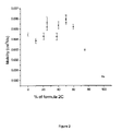
- FIG. 2 shows charge carrier mobility of mixtures according to Example 4.
- FIG. 3 shows charge carrier mobility of mixtures according to Example 5.
- test field effect transistors were prepared on pre-patterned Pt/Pd source and drain electrodes on a polyester substrate.
- the semiconductor composition according to the present invention (mixture of high and low molecular weight compounds) was dissolved one part into 99 parts of solvent, typically toluene, and spin coated onto the substrate at 1000 rpm for 20 s to yield a ⁇ 100 nm film. To ensure complete drying the sample was placed in an oven for 20 minutes at 100° C.
- a solution of a low permittivity perfluoropolymer, Cytop107M (Asahi Glass, Z-1700E01) was then spin-coated onto the semiconductor giving a thickness typically in the range 0.5 ⁇ m to 1 ⁇ m.
- the sample was placed once more in an oven at 100° C. to evaporate solvent from the insulator.
- a gold gate contact was defined over the device channel area by evaporation through a shadow mask.
- To determine the capacitance of the insulator layer a number of devices were prepared which consisted of a non-patterned Pt/Pd base layer, an insulator layer prepared in the same way as that on the FET device, and a top electrode of known geometry. The capacitance was measured using a hand-held multimeter, connected to the metal either side of the insulator.
- the voltages applied to the transistor are relative to the potential of the source electrode.
- a negative potential is applied to the gate
- positive charge carriers are accumulated in the semiconductor on the other side of the gate insulator.
- This is called the accumulation mode.
- the capacitance/area of the gate insulator C i determines the amount of the charge thus induced.
- V DS negative potential
- the accumulated carriers yield a source-drain current I DS which depends primarily on the density of accumulated carriers and, importantly, their mobility in the source-drain channel. Geometric factors such as the drain and source electrode configuration, size and distance also affect the current. Typically a range of gate and drain voltages are scanned during the study of the device.
- the source-drain current is described by equation 1.
- I DS ⁇ ⁇ ⁇ WC i L ⁇ ( ( V G - V 0 ) ⁇ V DS - V DS 2 2 ) + I ⁇ , eq . ⁇ 1
- V 0 is an offset voltage
- I ⁇ is an ohmic current independent of the gate voltage and is due to the finite conductivity of the material.
- the transistor sample was mounted in a sample holder. Microprobe connections were made to the gate, drain and source electrodes using Karl Suss PH100 miniature probe-heads. These were linked to a Hewlett-Packard 4155B parameter analyser.
- the drain voltage was set initially at ⁇ 2V and the gate voltage was scanned from +20 to ⁇ 40 V in 1 V steps, following this V D was set to ⁇ 20V and for a second time the gate was scanned from +20V to ⁇ 40V.
- the source-drain current varies linearly with V G .
- the field effect mobility can be calculated from the gradient (S) of I DS vs. V G given by equation 2.
- Mixtures 1-6 were made from the high molecular weight and low molecular weight compounds listed in Table 1 (50:50 parts by weight). The mobilities of the resultant mixtures are given, together with the % increase over the single component. It can be seen that substantial mobility increases are obtained with the mixtures and in the case of mixtures 3 and 5 the mobility more than doubled. The experiment tested compounds of formula 11A up to molecular weight of about 19000 which all showed the effect of increased mobility.
- Mixtures 14 & 15 not in accordance with the present invention were made from the high molecular weight and low molecular weight compounds listed in Table 3 (50:50 parts by weight). The mobilities of the resultant mixtures and the percentage change when compared with the high molecular weight compound on its own are given. The mobilities of the mixtures were found to be lower than the components on their own.
- Mixtures 16 & 17 were made from the high molecular weight and low molecular weight compounds listed in Table 4 (50:50 parts by weight). These tests were performed using chlorobenzene as a solvent for the organic semiconductor mixture.
- the dielectric used was polyisobutylene (Acros cat. No 29916-1000) spun from a solution in hexane. The mobility was determined using a gate potential of up to ⁇ 60V instead of ⁇ 40V as the dielectric thickness was greater than in the earlier examples. The mobilities of the resultant mixtures are given, together with the % increase over the single component. It can be seen that substantial mobility increases are obtained with the mixtures.
- Mixtures 18 & 19 were made from the high molecular weight and low molecular weight compounds listed in Table 5 (50:50 parts by weight), using the method of Example 6 above, except that in the case of mixture 18, the dielectric was CYTOP spun from a solution in toluene. The PIB dielectric in mixture 19 was spun from toluene. Measurements were carried out as in the above Example 6. The mobilities of the resultant mixtures are given in Table 5, together with the % increase over the single component. It can be seen that substantial mobility increases are again obtained with the mixtures.
- the high molecular weight compounds in this case were copolymers (formulae 12A and 12B below).
Landscapes
- Chemical & Material Sciences (AREA)
- Engineering & Computer Science (AREA)
- Materials Engineering (AREA)
- Organic Chemistry (AREA)
- Physics & Mathematics (AREA)
- Spectroscopy & Molecular Physics (AREA)
- Thin Film Transistor (AREA)
- Electroluminescent Light Sources (AREA)
- Compositions Of Macromolecular Compounds (AREA)
Applications Claiming Priority (6)
| Application Number | Priority Date | Filing Date | Title |
|---|---|---|---|
| GB0229660A GB0229660D0 (en) | 2002-12-20 | 2002-12-20 | Electronic devices |
| GB02296660.6 | 2002-12-20 | ||
| GB0229660.6 | 2002-12-20 | ||
| GB0310588A GB0310588D0 (en) | 2003-05-08 | 2003-05-08 | Improvements in and relating to organic semiconducting materials |
| GB0310588.9 | 2003-05-08 | ||
| PCT/GB2003/005521 WO2004057688A1 (en) | 2002-12-20 | 2003-12-18 | Improvements in and relating to organic semiconducting materials |
Publications (2)
| Publication Number | Publication Date |
|---|---|
| US20060155040A1 US20060155040A1 (en) | 2006-07-13 |
| US7718734B2 true US7718734B2 (en) | 2010-05-18 |
Family
ID=32683978
Family Applications (1)
| Application Number | Title | Priority Date | Filing Date |
|---|---|---|---|
| US10/539,745 Expired - Lifetime US7718734B2 (en) | 2002-12-20 | 2003-12-18 | Organic semiconducting materials |
Country Status (7)
| Country | Link |
|---|---|
| US (1) | US7718734B2 (de) |
| EP (1) | EP1579518B1 (de) |
| JP (1) | JP4739021B2 (de) |
| KR (1) | KR101247430B1 (de) |
| AU (1) | AU2003290272A1 (de) |
| TW (1) | TWI326926B (de) |
| WO (1) | WO2004057688A1 (de) |
Cited By (7)
| Publication number | Priority date | Publication date | Assignee | Title |
|---|---|---|---|---|
| US20070075630A1 (en) * | 2005-09-30 | 2007-04-05 | Florian Dotz | Organic compositions |
| US20080254568A1 (en) * | 2004-04-27 | 2008-10-16 | Koninklijke Philips Electronics, N.V. | Composition and Method of Forming a Device |
| US20110077373A1 (en) * | 2009-09-29 | 2011-03-31 | General Electric Company | Polymer and optoelectronic device comprising the same |
| US9356248B2 (en) | 2013-08-16 | 2016-05-31 | Palo Alto Research Center Incorporated | Organic thin-film transistor |
| GB2536426A (en) * | 2015-03-13 | 2016-09-21 | Cambridge Display Tech Ltd | Polymer blends for a semiconducting layer of an organic electronic device |
| US9853230B2 (en) | 2015-02-17 | 2017-12-26 | Xerox Corporation | Printable nanoparticle conductor ink with improved charge injection |
| US11702542B2 (en) | 2020-02-05 | 2023-07-18 | Samsung Display Co., Ltd. | Composition including polymer, interlayer prepared from the composition, and device comprising the same |
Families Citing this family (25)
| Publication number | Priority date | Publication date | Assignee | Title |
|---|---|---|---|---|
| CN100583437C (zh) | 2005-03-02 | 2010-01-20 | Nxp股份有限公司 | 电子器件及其使用 |
| NO324539B1 (no) * | 2005-06-14 | 2007-11-19 | Thin Film Electronics Asa | Fremgangsmate i fabrikasjonen av en ferroelektrisk minneinnretning |
| US7569415B2 (en) | 2005-09-30 | 2009-08-04 | Alcatel-Lucent Usa Inc. | Liquid phase fabrication of active devices including organic semiconductors |
| US7488834B2 (en) | 2005-09-30 | 2009-02-10 | Alcatel-Lucent Usa Inc. | Organic semiconductors |
| JP2009524226A (ja) | 2006-01-21 | 2009-06-25 | メルク パテント ゲゼルシャフト ミット ベシュレンクテル ハフツング | 有機半導体配合物を備える電子短チャネル装置 |
| US8138075B1 (en) | 2006-02-06 | 2012-03-20 | Eberlein Dietmar C | Systems and methods for the manufacture of flat panel devices |
| JP2009527924A (ja) * | 2006-02-24 | 2009-07-30 | プレックストロニクス インコーポレーティッド | 高性能ポリマー光起電力 |
| EP1936712A1 (de) * | 2006-12-23 | 2008-06-25 | ETH Zürich | Organische Feldeffekttransistoren mit polymerem Gate-Dielektrikum und Herstellungsverfahren dafür |
| JP5480510B2 (ja) | 2008-03-31 | 2014-04-23 | 住友化学株式会社 | 有機半導体組成物、並びに有機薄膜及びこれを備える有機薄膜素子 |
| GB2467316B (en) | 2009-01-28 | 2014-04-09 | Pragmatic Printing Ltd | Electronic devices, circuits and their manufacture |
| GB2473200B (en) | 2009-09-02 | 2014-03-05 | Pragmatic Printing Ltd | Structures comprising planar electronic devices |
| US8212243B2 (en) | 2010-01-22 | 2012-07-03 | Eastman Kodak Company | Organic semiconducting compositions and N-type semiconductor devices |
| RU2012156386A (ru) * | 2010-05-27 | 2014-07-10 | Мерк Патент Гмбх | Состав и способ получения органических электронных устройств |
| JP5812730B2 (ja) | 2010-07-13 | 2015-11-17 | 住友化学株式会社 | 有機半導体組成物、有機薄膜及びこれを備える有機薄膜トランジスタ |
| JP6061858B2 (ja) * | 2010-10-07 | 2017-01-18 | ジョージア・テック・リサーチ・コーポレーション | 電界効果トランジスタおよびその製造方法 |
| GB201021277D0 (en) | 2010-12-15 | 2011-01-26 | Cambridge Display Tech Ltd | Semiconductor blend |
| US9123899B2 (en) * | 2011-02-10 | 2015-09-01 | Samsung Electronics Co., Ltd. | Semiconductor compound |
| GB201304613D0 (en) * | 2013-03-14 | 2013-05-01 | Cambridge Display Tech Ltd | Blend |
| EP3135726A4 (de) * | 2014-04-21 | 2018-04-18 | Sumitomo Chemical Company, Limited | Zusammensetzung und polymerverbindung sowie organisches halbleiterelement mit dieser zusammensetzung und dieser polymerverbindung |
| JP6497387B2 (ja) * | 2014-04-21 | 2019-04-10 | 住友化学株式会社 | 膜および該膜を含有する有機半導体素子 |
| JP6648014B2 (ja) * | 2014-06-26 | 2020-02-14 | 保土谷化学工業株式会社 | 有機エレクトロルミネッセンス素子 |
| KR102287341B1 (ko) * | 2014-08-19 | 2021-08-06 | 삼성디스플레이 주식회사 | 유기 발광 소자 및 이를 포함하는 유기 발광 표시 장치 |
| JP6699141B2 (ja) * | 2015-11-27 | 2020-05-27 | 東ソー株式会社 | 有機半導体層形成用溶液、有機半導体層、および有機薄膜トランジスタ |
| JP6699142B2 (ja) * | 2015-11-27 | 2020-05-27 | 東ソー株式会社 | 有機半導体層形成用溶液、有機半導体層、および有機薄膜トランジスタ |
| EP3608981A4 (de) | 2017-03-21 | 2020-12-23 | Nippon Kayaku Kabushiki Kaisha | Organische halbleiterzusammensetzung, organische halbleiterdünnschicht und organischer dünnschichttransistor |
Citations (6)
| Publication number | Priority date | Publication date | Assignee | Title |
|---|---|---|---|---|
| WO1999032537A1 (en) | 1997-12-19 | 1999-07-01 | Avecia Limited | POLYMERIC MATERIAL COMPRISING N, P, S, As OR Se AND COMPOSITION FOR CHARGE TRANSPORT MATERIAL |
| WO1999054385A1 (en) | 1998-04-21 | 1999-10-28 | The Dow Chemical Company | Fluorene-containing polymers and electroluminescent devices therefrom |
| WO2000078843A1 (en) | 1997-12-19 | 2000-12-28 | Avecia Limited | Process for the isolation of polymer fractions |
| US20020058157A1 (en) * | 2000-11-10 | 2002-05-16 | Sumitomo Chemical Company, Limited | Polymeric fluorescent substance and polymer light-emitting device using the same |
| WO2002045184A1 (en) | 2000-11-28 | 2002-06-06 | Avecia Limited | Field effect transistors and materials and methods for their manufacture |
| US6605323B1 (en) | 1998-06-08 | 2003-08-12 | Aventis Research & Technologies Gmbh & Co. Kg | Monostable ferroelectric active matrix display |
Family Cites Families (5)
| Publication number | Priority date | Publication date | Assignee | Title |
|---|---|---|---|---|
| JPH0547211A (ja) * | 1991-03-14 | 1993-02-26 | Ricoh Co Ltd | 高分子電荷移動錯体 |
| JP3522771B2 (ja) * | 1991-03-22 | 2004-04-26 | 三菱電機株式会社 | インバータ |
| JP3883097B2 (ja) * | 1999-08-20 | 2007-02-21 | 株式会社リコー | 電子写真感光体、これを用いた画像形成装置および画像形成装置用プロセスカートリッジ |
| CN100526389C (zh) * | 2002-03-26 | 2009-08-12 | 大日本印刷株式会社 | 有机半导体材料、有机半导体构造物和有机半导体器件 |
| JP4545373B2 (ja) * | 2002-11-07 | 2010-09-15 | 旭化成株式会社 | 有機半導体薄膜及びその製造方法 |
-
2003
- 2003-12-18 AU AU2003290272A patent/AU2003290272A1/en not_active Abandoned
- 2003-12-18 WO PCT/GB2003/005521 patent/WO2004057688A1/en not_active Ceased
- 2003-12-18 KR KR1020057011665A patent/KR101247430B1/ko not_active Expired - Lifetime
- 2003-12-18 US US10/539,745 patent/US7718734B2/en not_active Expired - Lifetime
- 2003-12-18 JP JP2005502581A patent/JP4739021B2/ja not_active Expired - Lifetime
- 2003-12-18 EP EP03782638.5A patent/EP1579518B1/de not_active Expired - Lifetime
- 2003-12-19 TW TW092136244A patent/TWI326926B/zh not_active IP Right Cessation
Patent Citations (9)
| Publication number | Priority date | Publication date | Assignee | Title |
|---|---|---|---|---|
| US20010026878A1 (en) | 1997-05-21 | 2001-10-04 | Woo Edmund P. | Fluorene-containing polymers and electroluminescent devices therefrom |
| US6309763B1 (en) | 1997-05-21 | 2001-10-30 | The Dow Chemical Company | Fluorene-containing polymers and electroluminescent devices therefrom |
| WO1999032537A1 (en) | 1997-12-19 | 1999-07-01 | Avecia Limited | POLYMERIC MATERIAL COMPRISING N, P, S, As OR Se AND COMPOSITION FOR CHARGE TRANSPORT MATERIAL |
| WO2000078843A1 (en) | 1997-12-19 | 2000-12-28 | Avecia Limited | Process for the isolation of polymer fractions |
| WO1999054385A1 (en) | 1998-04-21 | 1999-10-28 | The Dow Chemical Company | Fluorene-containing polymers and electroluminescent devices therefrom |
| US6605323B1 (en) | 1998-06-08 | 2003-08-12 | Aventis Research & Technologies Gmbh & Co. Kg | Monostable ferroelectric active matrix display |
| US20020058157A1 (en) * | 2000-11-10 | 2002-05-16 | Sumitomo Chemical Company, Limited | Polymeric fluorescent substance and polymer light-emitting device using the same |
| WO2002045184A1 (en) | 2000-11-28 | 2002-06-06 | Avecia Limited | Field effect transistors and materials and methods for their manufacture |
| US20040038459A1 (en) | 2000-11-28 | 2004-02-26 | Brown Beverley Anne | Field effect transistors and materials and methods for their manufacture |
Non-Patent Citations (4)
| Title |
|---|
| Helbig et al., Patent Abstract of Germany, DE 19832943 A1, Feb. 3, 2000, 20 pages. |
| I. Levesque et al. "Organic tunable electroluminescen tdiodes from polyfluorene derivatives" 2001, Synthetic Metals, vol. 122, pp. 79-81. * |
| Oshima Katsunori, Patent Abstract of Japan, JP 55-090953, Jul. 10, 1980, 5 pages. |
| Shijie Liao et al., Patent Abstract of China, CN 1589964 A, Mar. 9, 2005, 9 pages. |
Cited By (11)
| Publication number | Priority date | Publication date | Assignee | Title |
|---|---|---|---|---|
| US20080254568A1 (en) * | 2004-04-27 | 2008-10-16 | Koninklijke Philips Electronics, N.V. | Composition and Method of Forming a Device |
| US8241946B2 (en) * | 2004-04-27 | 2012-08-14 | Creator Technology B.V. | Method of forming an organic semiconducting device by a melt technique |
| US20120273734A1 (en) * | 2004-04-27 | 2012-11-01 | Creator Technology B.V. | Composition for forming an organic semiconducting device |
| US8492192B2 (en) * | 2004-04-27 | 2013-07-23 | Creator Technology B.V. | Composition for forming an organic semiconducting device |
| US20070075630A1 (en) * | 2005-09-30 | 2007-04-05 | Florian Dotz | Organic compositions |
| US20110077373A1 (en) * | 2009-09-29 | 2011-03-31 | General Electric Company | Polymer and optoelectronic device comprising the same |
| US9356248B2 (en) | 2013-08-16 | 2016-05-31 | Palo Alto Research Center Incorporated | Organic thin-film transistor |
| US9853230B2 (en) | 2015-02-17 | 2017-12-26 | Xerox Corporation | Printable nanoparticle conductor ink with improved charge injection |
| GB2536426A (en) * | 2015-03-13 | 2016-09-21 | Cambridge Display Tech Ltd | Polymer blends for a semiconducting layer of an organic electronic device |
| US10249822B2 (en) | 2015-03-13 | 2019-04-02 | Cambridge Display Technology Limited | Polymer blends for a semiconducting layer of an organic electronic device |
| US11702542B2 (en) | 2020-02-05 | 2023-07-18 | Samsung Display Co., Ltd. | Composition including polymer, interlayer prepared from the composition, and device comprising the same |
Also Published As
| Publication number | Publication date |
|---|---|
| EP1579518A1 (de) | 2005-09-28 |
| KR20050107571A (ko) | 2005-11-14 |
| JP4739021B2 (ja) | 2011-08-03 |
| EP1579518B1 (de) | 2016-03-23 |
| TWI326926B (en) | 2010-07-01 |
| KR101247430B1 (ko) | 2013-03-25 |
| US20060155040A1 (en) | 2006-07-13 |
| TW200427120A (en) | 2004-12-01 |
| AU2003290272A1 (en) | 2004-07-14 |
| JP2006514710A (ja) | 2006-05-11 |
| WO2004057688A1 (en) | 2004-07-08 |
Similar Documents
| Publication | Publication Date | Title |
|---|---|---|
| US20060155040A1 (en) | Organic semiconducting materials | |
| US7095044B2 (en) | Field effect transistors and materials and methods for their manufacture | |
| TWI453963B (zh) | 包括有機半導體配方的短通道電子裝置 | |
| US10693072B2 (en) | Diazirine containing organic electronic compositions and device thereof | |
| US8119804B2 (en) | Organic semiconducting layers | |
| KR101932806B1 (ko) | 유기 반도체 조성물 | |
| US20050104058A1 (en) | Organic field effect transistor with an organic dielectric | |
| US8314416B2 (en) | Organic semiconductor formulation | |
| US7935960B2 (en) | Polyacene and semiconductor formulation | |
| AU2002220818A1 (en) | Field effect transistors and materials and methods for their manufacture | |
| KR20150041094A (ko) | 유기 반도성 제제 | |
| CN1739204B (zh) | 改进有机半导体材料及与其有关的改进 | |
| KR20080109066A (ko) | 펜타센 중합체 및 이의 전자 소자에서의 용도 |
Legal Events
| Date | Code | Title | Description |
|---|---|---|---|
| AS | Assignment |
Owner name: MERCK PATENT GMBH,GERMANY Free format text: ASSIGNMENT OF ASSIGNORS INTEREST;ASSIGNORS:VERES, JANOS;BROOKES, PAUL CRAIG;WILLIAMS, RICHARD THOMAS;AND OTHERS;REEL/FRAME:017795/0302 Effective date: 20050919 Owner name: MERCK PATENT GMBH, GERMANY Free format text: ASSIGNMENT OF ASSIGNORS INTEREST;ASSIGNORS:VERES, JANOS;BROOKES, PAUL CRAIG;WILLIAMS, RICHARD THOMAS;AND OTHERS;REEL/FRAME:017795/0302 Effective date: 20050919 |
|
| FEPP | Fee payment procedure |
Free format text: PAYOR NUMBER ASSIGNED (ORIGINAL EVENT CODE: ASPN); ENTITY STATUS OF PATENT OWNER: LARGE ENTITY |
|
| STCF | Information on status: patent grant |
Free format text: PATENTED CASE |
|
| FPAY | Fee payment |
Year of fee payment: 4 |
|
| MAFP | Maintenance fee payment |
Free format text: PAYMENT OF MAINTENANCE FEE, 8TH YEAR, LARGE ENTITY (ORIGINAL EVENT CODE: M1552) Year of fee payment: 8 |
|
| FEPP | Fee payment procedure |
Free format text: MAINTENANCE FEE REMINDER MAILED (ORIGINAL EVENT CODE: REM.); ENTITY STATUS OF PATENT OWNER: LARGE ENTITY |
|
| FEPP | Fee payment procedure |
Free format text: 11.5 YR SURCHARGE- LATE PMT W/IN 6 MO, LARGE ENTITY (ORIGINAL EVENT CODE: M1556); ENTITY STATUS OF PATENT OWNER: LARGE ENTITY |
|
| MAFP | Maintenance fee payment |
Free format text: PAYMENT OF MAINTENANCE FEE, 12TH YEAR, LARGE ENTITY (ORIGINAL EVENT CODE: M1553); ENTITY STATUS OF PATENT OWNER: LARGE ENTITY Year of fee payment: 12 |
|
| AS | Assignment |
Owner name: FLEXENABLE LTD., UNITED KINGDOM Free format text: ASSIGNMENT OF ASSIGNORS INTEREST;ASSIGNOR:MERCK PATENT GMBH;REEL/FRAME:063907/0525 Effective date: 20191112 |
|
| AS | Assignment |
Owner name: FLEXENABLE TECHNOLOGY LIMITED, UNITED KINGDOM Free format text: ASSIGNMENT OF ASSIGNORS INTEREST;ASSIGNOR:FLEXENABLE LTD.;REEL/FRAME:064279/0813 Effective date: 20230419 |