US7475165B2 - Semiconductor data storage apparatus - Google Patents
Semiconductor data storage apparatus Download PDFInfo
- Publication number
- US7475165B2 US7475165B2 US11/058,254 US5825405A US7475165B2 US 7475165 B2 US7475165 B2 US 7475165B2 US 5825405 A US5825405 A US 5825405A US 7475165 B2 US7475165 B2 US 7475165B2
- Authority
- US
- United States
- Prior art keywords
- analog module
- power supply
- external
- internal
- circuit
- Prior art date
- Legal status (The legal status is an assumption and is not a legal conclusion. Google has not performed a legal analysis and makes no representation as to the accuracy of the status listed.)
- Expired - Fee Related, expires
Links
Images


Classifications
-
- G—PHYSICS
- G11—INFORMATION STORAGE
- G11C—STATIC STORES
- G11C17/00—Read-only memories programmable only once; Semi-permanent stores, e.g. manually-replaceable information cards
- G11C17/14—Read-only memories programmable only once; Semi-permanent stores, e.g. manually-replaceable information cards in which contents are determined by selectively establishing, breaking or modifying connecting links by permanently altering the state of coupling elements, e.g. PROM
- G11C17/16—Read-only memories programmable only once; Semi-permanent stores, e.g. manually-replaceable information cards in which contents are determined by selectively establishing, breaking or modifying connecting links by permanently altering the state of coupling elements, e.g. PROM using electrically-fusible links
-
- G—PHYSICS
- G11—INFORMATION STORAGE
- G11C—STATIC STORES
- G11C16/00—Erasable programmable read-only memories
- G11C16/02—Erasable programmable read-only memories electrically programmable
- G11C16/06—Auxiliary circuits, e.g. for writing into memory
- G11C16/10—Programming or data input circuits
- G11C16/20—Initialising; Data preset; Chip identification
Definitions
- the present invention relates to a technology for reducing cost for a semiconductor data storage apparatus and, more particularly, to a technology which is effective when applied to cost reduction for a memory card using a nonvolatile memory.
- semiconductor data storage apparatus such as a CF (Compact Flash) card, smart media, a memory stick, and a multimedia card.
- CF Compact Flash
- a semiconductor data storage apparatus comes in various versions prepared for different purposes, which include a low-price version, a standard version, and a high-reliability/high-value-added version with an increased added value.
- a low-price version for example, an analog module including a power supply circuit, a clock generator circuit, and a power supply monitor circuit has preliminarily been mounted on a controller, thereby achieving cost reduction.
- a power supply circuit, a clock generator circuit, a power supply monitor circuit, and the like are not mounted on a controller but formed as an external analog module, thus providing a structure which further enhances reliability.
- some of a power supply circuit, a clock generator circuit, a power supply monitor circuit, and the like are formed as an internal analog module which is mounted on a controller, while the others are formed as an external analog module, thereby providing a structure which offers a balance between cost and reliability.
- Examples in which power supply circuits in nonvolatile semiconductor memories of this type are described in detail include one in which plural types of internal voltages are generated (Patent Document 1) and one in which trimming means for the pulse width of a write voltage is provided (Patent Document 2).
- Patent Document 1 Japanese Laid-Open Patent Publication No. Hei 07(1995)-176698 (U.S. Pat. No. 5,553,021)
- Patent Document 2 Japanese Laid-Open Patent Publication No. Hei 10(1998)-106276 (U. S. Pat. No. 6,091,640)
- the present invention is a semiconductor data storage apparatus comprising: one or more semiconductor memories; a data processing unit for reading data stored in the one or more semiconductor memories based on an operating program and giving an instruction to perform a specified process, a data write operation, or the like; and an external analog module connected externally to the data processing unit, wherein the data processing unit has an internal analog module and a switching element for making enable/disable settings for the internal analog module and the external analog module.
- the present invention is a semiconductor data storage apparatus comprising: one or more semiconductor memories; a data processing unit for reading data stored in the one or more semiconductor memories based on an operating program and giving an instruction to perform a specified process, a data write operation, or the like; and an external analog module connected externally to the data processing unit, wherein the data processing unit has an internal analog module and a switching element for making enable/disable settings for the internal analog module and the external analog module and the switching element performs enable/disable switching control depending on an operating mode of each of the semiconductor memories.
- FIG. 1 is a block diagram of a data processing system according to an embodiment of the present invention
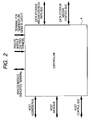
- FIG. 2 is an illustrative view showing a schematic layout of external connection terminals in a controller provided in the data processing system of FIG. 1 ;
- FIG. 3 is an illustrative view showing an example when fuses are used for the switching elements of the controller in the data processing system of FIG. 1 ;
- FIG. 4 is an illustrative view showing an example when the switching elements of the controller in the data processing system of FIG. 1 are composed of selectors;
- FIG. 5 is a flowchart showing an operation in the data processing system of FIG. 4 ;
- FIG. 6 is a view illustrating the controller when an internal analog module is selected as a result of the process of FIG. 5 ;
- FIG. 7 is a view illustrating the processing of select control signals at analog module dedicated terminals in the controller of FIG. 2 ;
- FIG. 8 is a view illustrating the controller when an external analog module is selected as a result of the process of FIG. 5 ;
- FIG. 9 is an illustrative view showing an example when switching is performed between the internal module and the external module based on the number of data storage media in connection in the data processing system of FIG. 1 ;
- FIG. 10 is a flow chart showing an operation in the data processing system of FIG. 9 ;
- FIG. 11 is an illustrative view showing an exemplary case where the controller in the data processing system of FIG. 1 controls the switching of the selectors based on the current level of an internal power supply voltage;
- FIG. 12 is an illustrative view showing an exemplary case where the controller in the data processing system of FIG. 1 controls the switching of the selectors based on the voltage level of the internal power supply voltage;
- FIG. 13 is an illustrative view showing an exemplary case where the controller in the data processing system of FIG. 1 controls the switching of the selectors based on the current level of a power supply voltage;
- FIG. 14 is an illustrative view showing an exemplary case where the controller in the data processing system of FIG. 1 controls the switching of the selectors based on the voltage level of the power supply voltage;
- FIG. 15 is a timing chart showing an example of current-value/voltage-value fluctuations in the power supply voltage after the turning ON of a power supply and in the internal power supply voltage in the data processing system of FIG. 1 ;
- FIG. 16 is a flow chart showing a process in the controller in the data processing system of FIG. 11 ;
- FIG. 17 is a flow chart showing a process in the controller in the data processing system of FIG. 12 ;
- FIG. 18 is a flow chart showing a process in the controller in the data processing system of FIG. 13 ;
- FIG. 19 is a flow chart showing a process in the controller in the data processing system of FIG. 14 ;
- FIG. 20 is an illustrative view showing an example when the controller in the data processing system of FIG. 1 controls the switching of the selectors based on a command from a host;
- FIG. 21 is a flow chart showing a process in the data processing system of FIG. 20 ;
- FIG. 22 is an illustrative view when the host in the data processing system of FIG. 1 directly controls the switching of the selectors in the data processing system of FIG. 1 ;
- FIG. 23 is a flow chart showing a process in the data processing system of FIG. 22 ;
- FIG. 24 is an illustrative when the data processing system of FIG. 1 controls the switching of the selectors by sensing a temperature
- FIG. 25 is a flow chart showing a process in the data processing system of FIG. 24 .
- FIG. 1 is a block diagram of a data processing system according to an embodiment of the present invention.
- FIG. 2 is an illustrative view showing a schematic layout of external connection terminals in a controller provided in the data processing system of FIG. 1 .
- FIG. 3 is an illustrative view showing an example when fuses are used for the switching elements of the controller in the data processing system of FIG. 1 .
- FIG. 4 is an illustrative view showing an example when the switching elements of the controller in the data processing system of FIG. 1 are composed of selectors.
- FIG. 5 is a flow chart showing an operation in the data processing system of FIG. 4 .
- FIG. 6 is a view illustrating the controller when an internal analog module is selected as a result of the process of FIG. 5 .
- FIG. 7 is a view illustrating the processing of select control signals at analog module dedicated terminals in the controller of FIG. 2 .
- FIG. 8 is a view illustrating the controller when an external analog module is selected as a result of the process of FIG. 5 .
- FIG. 9 is an illustrative view showing an example when switching is performed between the internal module and the external module based on the number of data storage media in connection in the data processing system of FIG. 1 .
- FIG. 10 is a flow chart showing an operation in the data processing system of FIG. 9 .
- FIG. 11 is an illustrative view showing an exemplary case where the controller in the data processing system of FIG. 1 controls the switching of the selectors based on the current level of an internal power supply voltage.
- FIG. 12 is an illustrative view showing an exemplary case where the controller in the data processing system of FIG. 1 controls the switching of the selectors based on the voltage level of the internal power supply voltage.
- FIG. 13 is an illustrative view showing an exemplary case where the controller in the data processing system of FIG. 1 controls the switching of the selectors based on the current level of a power supply voltage.
- FIG. 14 is an illustrative view showing an exemplary case where the controller in the data processing system of FIG. 1 controls the switching of the selectors based on the voltage level of the power supply voltage.
- FIG. 12 is an illustrative view showing an exemplary case where the controller in the data processing system of FIG. 1 controls the switching of the selectors based on the voltage level of the internal power supply voltage.
- FIG. 13 is an illustrative view showing an exemplary case where the controller in the data processing system of FIG. 1 controls the switching of the selectors based on the current level of a power supply voltage.
- FIG. 15 is a timing chart showing an example of current-value/voltage-value fluctuations in the power supply voltage after the turning ON of a power supply and in the internal power supply voltage in the data processing system of FIG. 1 .
- FIG. 16 is a flow chart showing a process in the controller in the data processing system of FIG. 11 .
- FIG. 17 is a flow chart showing a process in the controller in the data processing system of FIG. 12 .
- FIG. 18 is a flow chart showing a process in the controller in the data processing system of FIG. 13 .
- FIG. 19 is a flow chart showing a process in the controller in the data processing system of FIG. 14 .
- FIG. 20 is an illustrative view showing an example when the controller in the data processing system of FIG.
- FIG. 21 is a flow chart showing a process in the data processing system of FIG. 20 .
- FIG. 22 is an illustrative view when the host in the data processing system of FIG. 1 directly controls the switching of the selectors in the data processing system of FIG. 1 .
- FIG. 23 is a flow chart showing a process in the data processing system of FIG. 22 .
- FIG. 24 is an illustrative when the data processing system of FIG. 1 controls the switching of the selectors by sensing a temperature.
- FIG. 25 is a flow chart showing a process in the data processing system of FIG. 24 .
- a data processing system 1 is composed of a host (data processing apparatus) 2 and a semiconductor data storage apparatus 3 .
- the host 2 is composed of a data processing apparatus such as a personal computer or a multi-function terminal.
- the semiconductor data storage apparatus 3 is composed of a memory card used as an external storage media for the host 2 .
- the semiconductor data storage apparatus 3 is composed of a controller (data processing unit) 4 , an external power supply circuit (external analog module) 5 , an external power supply monitor circuit (external analog module) 6 , a clock generator element (external analog module, external clock oscillator circuit) 7 , and a data storage medium (semiconductor memory) 8 .
- the data storage medium 8 is composed of a semiconductor memory such as, e.g., a flash memory (FLASH EEPROM). Although a structure provided with one data storage medium 8 is shown herein, a plurality of the data storage media 8 may also be provided.
- a semiconductor memory such as, e.g., a flash memory (FLASH EEPROM).
- the data storage medium 8 may also be a memory other than the flash memory mentioned above. Any memory that can store data, such as an SRAM (Static Random Access Memory), a DRAM (Dynamic RAM), an MRAM (Magnetroresistive RAM), or an EPROM (Erasable and Programmable Read Only Memory), may be used appropriately.
- SRAM Static Random Access Memory
- DRAM Dynamic RAM
- MRAM Magnetic RAM
- EPROM Erasable and Programmable Read Only Memory
- the present embodiment has provided a controller which is separate and distinct from the semiconductor memory, the two and peripheral parts may also be embedded appropriately in a semiconductor.
- the controller 4 reads a program, data, and the like stored in the data storage medium 8 based on an operating program and gives an instruction to perform a specified process, a data write operation, or the like.
- the external power supply circuit 5 , the external power supply monitor circuit 6 , the clock generator element 7 , and the like are externally connected to the controller 4 .
- the external power supply circuit 5 is composed of, e.g., a power supply IC and generates an internal power supply voltage Vdd 1 from a power supply voltage VCC supplied from the host 2 or the like.
- the external power supply monitor circuit 6 is a so-called reset IC which monitors an internal power supply voltage Vdd 1 or an internal power supply voltage Vdd 2 , which will be described later, and generates a reset signal when a voltage reaches a given level or lower.
- the clock generator element 7 is composed of, e.g., a crystal oscillator which generates a clock signal serving as a system clock for the controller 4 and supplies the generated clock signal to a control circuit (control unit, memory sensor unit) 9 .
- the controller 4 is composed of the control circuit 9 , the internal power supply circuit (internal analog module) 10 , an internal power supply monitor circuit (internal analog module) 11 , a self-excited oscillator circuit (internal analog module, internal clock oscillator circuit) 12 , switching elements 13 to 15 , and the like.
- the internal power supply circuit 10 , the internal power supply monitor circuit 11 , and the self-excited oscillator circuit 12 constitute an internal analog module provided in the controller 4 .
- the control circuit 9 administers all control operations in the controller 4 .
- the internal power supply circuit 10 generates the internal power supply voltage Vdd 2 from the power supply voltage VCC supplied from the host 2 or the like.
- the internal power supply monitor circuit 11 monitors the internal power supply voltage Vdd 1 or the internal power supply voltage Vdd 2 and generates a reset signal when a voltage reaches a given level or lower.
- the self-excited oscillator circuit 12 generates the clock signal at a given frequency and supplies the generated clock signal as the system clock to the control circuit 9 .
- the internal power supply voltage Vdd 1 and the internal power supply voltage Vdd 2 are connected to the switching element 13 to be inputted thereto.
- the switching element 13 selectively outputs either one of the internal power supply voltage Vdd 1 and the internal power supply voltage Vdd 2 and supplies the internal power supply voltage Vdd 1 or Vdd 2 as an internal power supply voltage Vdd to the external power supply monitor circuit 6 , the internal power supply monitor circuit 11 , the data storage medium 8 , the control circuit 9 , and the like.
- the external power supply monitor circuit 6 and the internal power supply monitor circuit 11 are connected to the switching element 14 .
- the switching element 14 selects either of the reset signal outputted from the external power supply monitor circuit 6 and the reset signal outputted from the internal power supply monitor circuit 11 and outputs the selected reset signal to the control circuit 9 .
- the clock generator element 7 and the self-excited oscillator circuit 12 are connected to the switching element 15 .
- the switching element 15 selects either of the clock signal outputted from the clock generator element 7 and the clock signal outputted from the self-excited oscillator circuit 12 and outputs the selected clock signal as a clock signal CLK to the control circuit 9 .
- FIG. 2 is an illustrative view showing a schematic layout of external connection terminals in the controller 4 .
- the controller 4 comprises a host address bus terminal, a host data bus terminal, a host control bus terminal, a data storage medium address/data bus terminal, a data storage medium control bus terminal, analog module dedicated terminals, analog module control terminals, a terminal for temperature sensor circuit, and the like.
- the host address bus terminal, the host data bus terminal, and the host control bus terminal are terminals used to access the host 2 by using an address signal, a data signal, and a control signal.
- the data storage medium address/data bus terminal and the data storage medium control bus terminal are terminals used to access the data storage medium 8 by using address/data signals and a control signal.
- the analog module dedicated terminals comprises: a terminal connected to the external module including the external power supply circuit 5 , the external power supply monitor circuit 6 , and the clock generator element 7 ; and a terminal which is necessary when the internal module including the internal power supply circuit 10 , the internal power supply monitor circuit 11 , and the self-excited oscillator circuit 12 is used.
- the analog module control terminals are terminals to which select control signals C 1 to C 3 used to control the switching elements 13 to 15 are inputted.
- the terminal for temperature sensor circuit is a terminal connected to a temperature sensor circuit 3 a (see FIG. 24 ) for measuring the temperature of an atmosphere in the semiconductor data storage apparatus 3 .
- FIG. 3 is an illustrative view showing an example when the switching elements 13 to 15 provided in the controller 4 of the data processing system 1 are composed of fuses (fuse elements) F 1 to F 6 .
- one connecting portion of the fuse 1 is connected to the external power supply circuit 5 and one connecting portion of the fuse F 2 is connected to the other connecting portion of the fuse F 1 , while the other connecting portion of the fuse F 2 is connected to the internal power supply circuit 10 , as shown in the drawing.
- the connecting portion between the fuses F 1 and F 2 serves as the output portion of the switching element 13 , which is connected to each of the external power supply monitor circuit 6 , the internal power supply monitor circuit 11 , the data storage medium 8 , the control circuit 9 , and the like.
- one connecting portion of the fuse F 3 is connected to the external power supply monitor circuit 6 and one connecting portion of the fuse F 4 is connected to the other connecting portion of the fuse F 3 , while the other connecting portion of the fuse F 4 is connected to the internal power supply monitor circuit 11 .
- the connecting portion between the fuses F 3 and F 4 is the output portion of the switching element 14 , which is connected to each of the control circuit 9 and the self-excited oscillator circuit 12 .
- one connecting portion of the fuse F 5 is connected to the clock generator element 7 and one connecting portion of the fuse F 6 is connected to the other connecting portion of the fuse F 5 , while the other connecting portion of the fuse F 6 is connected to the self-excited oscillator circuit 12 .
- the connecting portion between the fuses F 5 and F 6 is the output portion of the switching element 15 , which is connected to the control circuit 9 .
- the fuse F 2 is disconnected, while the fuse F 1 is left in the connected state.
- the external power supply monitor circuit 6 is selected by disconnecting the fuse F 4 .
- the self-excited oscillator circuit 12 is selected by disconnecting the fuse F 5 .
- each of the external analog module and the internal analog modules can be used selectively in accordance with a purpose by selecting the external power supply circuit 5 , the external power supply monitor circuit 6 , and the clock generator element 7 to make provisions for a large current if the semiconductor data storage apparatus 3 is in, e.g., a high-value-added version which allows a high-speed data access thereto using an interleave operation or by using the internal power supply circuit 10 , the internal power supply monitor circuit 11 , and the self-excited oscillator circuit 12 if the semiconductor data storage apparatus 3 is in, e.g., a low-price version which does not use the interleave operation.
- the same controller 4 can be used successfully even when either of the external analog module and the internal analog module is used. This achieves significant reductions in manufacturing cost and production management cost.
- FIG. 4 is an illustrative view showing an example when the switching elements 13 to 15 provided in the controller 4 in the data processing system 1 are composed of selectors S 1 to S 3 .
- the selector S 1 composing the switching element 13 has one input portion connected to the external power supply circuit 5 and the other input portion connected to the internal power supply circuit 10 .
- the selector S 1 performs switching between output signals (the internal power supply voltages Vdd 1 and Vdd 2 ) based on the select control signal C 1 inputted via the analog module control terminal provided in the controller 4 .
- the selector S 2 composing the switching element 14 has one input portion connected to the external power supply monitor circuit 6 and the other input portion connected to the internal power supply monitor circuit 11 .
- the selector S 2 selects either of the external power supply monitor circuit 6 and the internal power supply monitor circuit 11 based on the select control signal C 2 inputted via the analog module control terminal and connects the selected circuit.
- the selector S 3 composing the switching element 15 has one input portion connected to the clock generator element 7 and the other input portion connected to the self-excited oscillator circuit 12 .
- the selector S 3 selects either of the clock generator element 7 and the self-excited oscillator circuit 12 based on the select control signal C 3 inputted via the analog module control terminal and connects the selected element or circuit.
- Step S 101 when the power supply is turned ON (Step S 101 ), the selector S 1 recognizes the voltage level (‘0’ or ‘1’) of the select control signal C 1 (Step S 102 ). When the select control signal C 1 is ‘1’, the selector S 1 performs switching such that the internal power supply voltage Vdd 1 generated by the external power supply circuit 5 is outputted (Step S 103 ).
- Step S 104 When the select control signal C 1 is ‘0’ in the process of Step S 102 , on the other hand, the selector S 1 performs switching such that the internal power supply voltage Vdd 2 generated by the internal power supply circuit 10 is outputted (Step S 104 ).
- the selector S 2 recognizes the voltage level of the select control signal C 2 (Step S 105 ).
- the selector S 2 performs switching such that the external power supply monitor circuit 6 is connected (Step S 106 ).
- the selector S 2 performs switching such that the internal power supply monitor circuit 11 is connected (Step S 107 ).
- the selector S 3 recognizes the voltage level of the select control signal C 3 (Step S 108 ).
- the selector S 3 performs switching such that the clock signal generated by the clock generator element 7 is outputted (Step S 109 ).
- the selector S 3 performs switching such that the clock signal generated by the self-excited oscillator circuit 12 is outputted (Step S 110 ). The switching process performed by the controller 4 is thus ended.
- FIG. 6 is a view illustrating the controller 4 when the internal analog module (the internal power supply circuit 10 , the internal power supply monitor circuit 11 , and the self-excited oscillator circuit 12 ) is selected.
- the power supply voltage VCC supplied from the host 2 is inputted to the internal power supply circuit 10 via the analog module dedicated terminal.
- the internal power supply voltage Vdd 2 ( FIG. 1 ) generated by the internal power supply circuit 10 is supplied to the data storage medium 8 via the analog module dedicated terminal.
- FIG. 7 is a view illustrating the processing of the select control signals C 1 to C 3 at the analog module dedicated terminals.
- the setting of each of the select control signals C 1 to C 1 to ‘1’ or ‘0’ is made by connecting the corresponding one of the analog module control terminals to the internal power supply voltage Vdd or to a reference voltage VSS using bonding options.
- FIG. 8 is a view illustrating the controller 4 when the external analog module (the external power supply circuit 5 , the external power supply monitor circuit 6 , and the clock generator element 7 ) is selected.
- the external power supply circuit 5 generates the internal power supply voltage Vdd 1 ( FIG. 1 ) from the power supply voltage VCC supplied from the host 2 .
- This provides the structure in which the external power supply circuit 5 , the external power supply monitor circuit 6 , and the clock generator element 7 are connected to the controller 4 via the analog module dedicated terminals.
- the same controller 4 can be used successfully by providing the selectors S 1 to S 3 even when either of the external analog module and the internal analog module is used. This achieves significant reductions in manufacturing cost and production management cost.
- FIG. 9 is an illustrative view showing an example when the control circuit 9 in the data processing system 1 automatically senses the number of the data storage media 8 in connection and performs switching between the internal analog module and the external analog module based on the result of sensing.
- the switching elements 13 to 15 are composed of the selectors S 1 to S 3 and the connecting configuration thereof is also the same as in FIG. 4 , as shown in the drawing. A different point is that the selectors S 1 to S 3 are connected to receive control signals CC 1 to CC 3 outputted from the control circuit 9 .
- Step S 201 when the power supply is turned ON (Step S 201 ), the controller 4 selects the internal analog module (the internal power supply circuit 10 , the internal power supply monitor circuit 11 , and the self-excited oscillator circuit 12 ) (Step S 202 ).
- the controller 4 selects the internal analog module in the default state upon the turning ON of the power supply in this process of Step S 202
- the controller 4 it is also possible for the controller 4 to select the external analog module upon the turning ON of the power supply.
- the default state may also be set appropriately by using the select control signals C 1 to C 3 inputted via the analog module dedicated terminals described above.
- Step S 203 the control circuit 9 reads data from, e.g., the data storage media 8 and senses the number of the data storage media 8 in connection.
- the number of the data storage media 8 in connection is sensed by, e.g., reading a data table stored in each of the data storage media 8 therefrom to read data in a reset process and checking the status, checking the register, and reading the maker and the type specific code.
- the controller 4 judges whether or not the sensed number of the data storage media 8 is N or larger (Step S 204 ). If the number is N or more, the controller 4 outputs the control signals CC 1 to CC 3 to the selectors S 1 to S 3 and selects the external analog module (Step S 205 ).
- the controller 4 If the sensed number of the data storage media 8 is smaller than N, the controller 4 outputs the control signals CC 1 to CC 3 to the selectors S 1 to S 3 such that the internal analog module is selected (Step S 206 ). By the foregoing operation, the selection process performed by the controller 4 is ended.
- FIG. 11 is an illustrative view showing an exemplary case where the controller 4 in the data processing system 1 controls the switching of the selectors S 1 to S 3 depending on the current level of the internal power supply voltage Vdd.
- a different point from the data processing system 1 of FIG. 4 is that a current sensor circuit (current sensor unit) 9 a for sensing the current level of the internal power supply voltage Vdd is newly provided in the control circuit 9 , as shown in the drawing.
- the connection of the selectors S 1 to S 3 is controlled by using the control signals CC 1 to CC 3 outputted from the control circuit 9 in the same manner as in FIG. 9 .
- FIG. 12 is an illustrative view showing an exemplary case where the controller 4 in the data processing system 1 controls the switching of the selectors S 1 to S 3 depending on the voltage level of the internal power supply voltage Vdd.
- a voltage sensor circuit (voltage sensor unit) 9 b is newly provided in the control circuit 9 .
- the voltage sensor circuit 9 b judges whether or not the voltage level of the internal power supply voltage Vdd is higher than a threshold voltage VDET.
- FIG. 13 is an illustrative view showing an exemplary case where the controller 4 in the data processing system 1 controls the switching of the selectors S 1 to S 3 depending on the current level of the power supply voltage VCC supplied from the host 2 .
- a current sensor circuit (current sensor unit) 9 c for sensing the current level of the power supply voltage VCC is newly provided in the control circuit 9 .
- FIG. 14 is an illustrative view showing an exemplary case where the controller 4 in the data processing system 1 controls the switching of the selectors S 1 to S 3 depending on the voltage level of the power supply voltage VCC supplied from the host 2 .
- a voltage sensor circuit (voltage sensor unit) 9 d for sensing the voltage level of the power supply voltage VCC is newly provided in the control circuit 9 .
- the voltage sensor circuit 9 d judges whether or not the voltage level of the power supply voltage VCC is higher than the threshold voltage VDET.
- FIG. 15 is a timing chart showing an example of current-value/voltage-value fluctuations in the power supply voltage VCC after the turning ON of the power supply and in the internal power supply voltage Vdd.
- FIG. 15 shows, in a descending order, the timings of the power supply voltage VCC, the internal power supply voltage Vdd, sensing results from the voltage sensor circuits 9 b and 9 d, a reset signal/RESET inputted to the controller 4 , and respective signals for the currents Icc/Idd of the power supply voltage VCC and the internal power supply voltage Vdd.
- the read operation in the initial access during the reset process causes great fluctuations in the power supply voltage VCC, the internal power supply voltage Vdd, the current Icc, and the current Idd.
- the voltage sensor circuits 9 b and 9 d sense the respective fluctuations in the power supply voltage VCC and the internal power supply voltage Vdd, whereby switching is performed between the external analog module and the internal analog module.
- the current sensor circuits 9 a and 9 c sense the respective fluctuations in the currents Icc and Idd, whereby switching is performed between the external analog module and the internal analog module.
- Each of the current sensor circuits 9 a and 9 c is capable of preliminarily sensing a factor which causes a voltage drop so that reliability is enhanced.
- Each of the voltage sensor circuits 9 b and 9 d can be constructed in a relatively small scale so that cost is suppressed.
- FIG. 16 is a flow chart showing a process in the controller 4 provided with the current sensor circuit 9 a.
- Step S 301 when the power supply is turned ON (Step S 301 ), the controller 4 selects the internal analog module according to the default setting (Step S 302 ).
- the default state may be set such that the controller 4 selects the external analog module upon the turning ON of the power supply.
- the default state may also be set by using the select control signals C 1 to C 3 inputted via the analog module dedicated terminals mentioned above.
- Step S 303 when the current sensor circuit 9 senses that the current of the internal power supply voltage Vdd becomes a threshold current or more in an initial access to the data storage medium 8 (Step S 303 ), the current sensor circuit 9 a outputs a sense signal to the control circuit 9 .
- control circuit 9 Upon receipt of the sense signal, the control circuit 9 outputs the control signals CC 1 to CC 3 as ‘1’ to the selectors S 1 to S 3 and performs a control operation for switching from the internal analog module to the external analog module (Step S 304 ).
- FIG. 17 is a flow chart showing a process in the controller 4 provided with the voltage sensor circuit 9 b.
- Step S 401 when the power supply is turned ON (Step S 401 ), the controller 4 selects the internal analog module according to the default setting (Step S 402 ).
- the default state may be set such that the controller 4 selects the external analog module upon the turning ON of the power supply.
- the default state may also be set by using the select control signals C 1 to C 3 inputted via the analog module dedicated terminals mentioned above.
- the voltage sensor circuit 9 b When the voltage sensor circuit 9 b senses that the voltage level of the internal power supply voltage Vdd becomes the threshold voltage VDET or less in an initial access to the data storage medium 8 after the end of the power-on reset process (Step S 403 ), the voltage sensor circuit 9 b outputs a sense signal to the control circuit 9 .
- control circuit 9 Upon receipt of the sense signal, the control circuit 9 outputs the control signals CC 1 to CC 3 as ‘1’ to the selectors S 1 to S 3 and performs a control operation for switching from the internal analog module to the external analog module (Step S 404 ).
- FIG. 18 is a flow chart showing a process in the controller 4 provided with the current sensor circuit 9 c.
- Step S 501 when the power supply is turned ON (Step S 501 ), the controller 4 selects the internal analog module according to the default setting (Step S 502 ).
- the default state may be set such that the external analog module is similarly selected upon the turning ON of the power supply.
- the default state may also be set by using the select control signals C 1 to C 3 .
- the current sensor circuit 9 c When the current sensor circuit 9 c senses that the current of the power supply voltage VCC becomes the threshold current or more in an initial access to the data storage medium 8 after the end of the power-on reset process (Step S 503 ), the current sensor circuit 9 c outputs a sense signal to the control circuit 9 .
- control circuit 9 Upon receipt of the sense signal, the control circuit 9 outputs the control signals CC 1 to CC 3 as ‘1’ to the selectors S 1 to S 3 and performs a control operation for switching from the internal analog module to the external analog module (Step S 504 ).
- FIG. 19 is a flow chart showing a process in the controller 4 provided with the voltage sensor circuit 9 d.
- Step S 601 when the power supply is turned ON (Step S 601 ), the controller 4 selects the internal analog module according to the default setting (Step S 602 ).
- the default state may be set such that the external analog module is selected or by using the select control signals C 1 to C 3 mentioned above.
- the voltage sensor circuit 9 d When the voltage sensor circuit 9 d senses that the voltage level of the power supply voltage VCC becomes the threshold voltage VDET or less in an initial access to the data storage medium 8 after the end of the power-on reset process (Step S 603 ), the voltage sensor circuit 9 d outputs a sense signal to the control circuit 9 .
- control circuit 9 Upon receipt of the sense signal, the control circuit 9 outputs the control signals CC 1 to CC 3 as ‘1’ to the selectors S 1 to S 3 and performs a control operation for switching from the internal analog module to the external analog module (Step S 604 ).
- FIG. 20 is an illustrative view showing an exemplary case where the controller 4 in the data processing system 1 controls the switching of the selectors S 1 to S 3 based on a command issued from the host 2 .
- the settings for controlling the switching of the selectors S 1 to S 3 are stored in a register 9 e provided in the control circuit 9 .
- FIG. 21 is a flow chart showing the operation of the data processing system 1 which controls the switching of the selectors S 1 to S 3 based on the command.
- Step S 701 When the power supply is turned ON (Step S 701 ), the controller 4 selects the internal analog module according to the default setting (Step S 702 ).
- the default state may also be set herein such that the controller 4 selects the external analog module upon the turning ON of the power supply.
- the default state may also be set by using the select control signals C 1 to C 3 inputted via the analog module dedicated terminals mentioned above.
- the host 2 issues a command by setting the register 9 e of the control circuit 9 in response to a command request from the semiconductor data storage apparatus 3 (Step S 703 ).
- the switching of the selectors S 1 to S 3 can be performed with higher-speed timing.
- control circuit 9 outputs the control signals CC 1 to CC 3 based on the command set to the register 9 e and controls the switching of the selectors S 1 to S 3 (Step S 704 ).
- FIG. 22 is a view illustrating the data processing system 1 in which the host 2 directly controls the switching of the selectors S 1 to S 3 .
- connection is provided such that the control signals CC 1 to CC 3 for controlling the switching of the selectors S 1 to S 3 are outputted directly from the host 2 .
- Step S 801 When the power supply is turned ON (Step S 801 ), the controller 4 selects the internal analog module according to the default setting (Step S 802 ).
- the default state may be set such that the controller 4 selects the external analog module upon the turning ON of the power supply.
- the default state may also be set by using the select control signals C 1 to C 3 inputted via the analog module dedicated terminals mentioned above.
- the host 2 outputs the control signals CC 1 to CC 3 to the selectors S 1 to S 3 and performs the switching of the selectors S 1 to S 3 (Step S 803 ).
- FIG. 24 is a view illustrating the data processing system 1 in which the switching of the selectors S 1 to S 3 is controlled based on the temperature of an atmosphere in the semiconductor data storage apparatus 3 .
- the semiconductor data storage apparatus 3 is provided with a temperature sensor circuit 3 a.
- the temperature sensor circuit 3 a senses the temperature of the atmosphere in the semiconductor data storage apparatus 3 .
- the temperature sensor circuit 3 a is connected to output the sensed temperature to the control circuit 9 via the terminal for temperature sensor circuit ( FIG. 2 ).
- Step S 901 when the power supply is turned ON (Step S 901 ), the controller 4 selects the internal analog module according to the default setting (Step S 902 ).
- the default state may also be set herein such that the controller 4 selects the external analog module upon the turning ON of the power supply.
- the default state may also be set by using the select control signals C 1 to C 3 inputted via the analog module dedicated terminals mentioned above.
- the temperature sensor circuit 3 a monitors the temperature of the atmosphere in the semiconductor data storage apparatus 3 and outputs the monitored temperature to the control circuit 9 .
- the control circuit 9 judges whether the inputted sensed temperature is not less than a first specified value (e.g., about 60° C.) or not more than a second specified value (e.g., about 0° C.) (Step S 903 ).
- control circuit 9 When the sensed temperature becomes not less than the first specified value or not more than the second specified value, the control circuit 9 outputs the control signals CC 1 to CC 3 to the selectors S 1 to S 3 and performs a control operation for switching to the external analog module (Step S 904 ).
- the reliability of the semiconductor data storage apparatus 3 can be enhanced.
- the present embodiment can use the common controller 4 to support the external analog module and the internal analog module and significantly reduce the manufacturing cost and the production management cost.
- a technology for controlling the switching of an analog module according to the present invention is suitable for a technology for reducing production cost for a semiconductor data storage apparatus.
Landscapes
- Semiconductor Integrated Circuits (AREA)
- Memory System (AREA)
- Techniques For Improving Reliability Of Storages (AREA)
Applications Claiming Priority (2)
| Application Number | Priority Date | Filing Date | Title |
|---|---|---|---|
| JP2004044051A JP2005234935A (ja) | 2004-02-20 | 2004-02-20 | 情報記憶装置 |
| JP2004-044051 | 2004-02-20 |
Publications (2)
| Publication Number | Publication Date |
|---|---|
| US20050185488A1 US20050185488A1 (en) | 2005-08-25 |
| US7475165B2 true US7475165B2 (en) | 2009-01-06 |
Family
ID=34858037
Family Applications (1)
| Application Number | Title | Priority Date | Filing Date |
|---|---|---|---|
| US11/058,254 Expired - Fee Related US7475165B2 (en) | 2004-02-20 | 2005-02-16 | Semiconductor data storage apparatus |
Country Status (3)
| Country | Link |
|---|---|
| US (1) | US7475165B2 (ja) |
| JP (1) | JP2005234935A (ja) |
| TW (1) | TW200602993A (ja) |
Cited By (3)
| Publication number | Priority date | Publication date | Assignee | Title |
|---|---|---|---|---|
| US20090307390A1 (en) * | 2008-06-04 | 2009-12-10 | Broadcom Corporation | Access of built-in peripheral components by internal and external bus pathways |
| US20110211385A1 (en) * | 2008-06-27 | 2011-09-01 | Renesas Electronics Corporation | Semiconductor device |
| US8228116B2 (en) * | 2009-03-31 | 2012-07-24 | Fujitsu Limited | Semiconductor integrated circuit and power supply voltage control method |
Families Citing this family (5)
| Publication number | Priority date | Publication date | Assignee | Title |
|---|---|---|---|---|
| DE19903987A1 (de) * | 1999-02-02 | 2000-08-10 | Friedrich Boelsing | Verfahren zur reduktiven Dehalogenierung flüssiger oder fester Halogenkohlenwasserstoffe |
| US7793059B2 (en) * | 2006-01-18 | 2010-09-07 | Apple Inc. | Interleaving policies for flash memory |
| KR100846387B1 (ko) * | 2006-05-31 | 2008-07-15 | 주식회사 하이닉스반도체 | 반도체 메모리 소자의 온도 정보 출력 장치 |
| US7516293B2 (en) * | 2006-09-08 | 2009-04-07 | International Business Machines Corporation | Increased performance using mixed memory types |
| KR101529291B1 (ko) * | 2008-02-27 | 2015-06-17 | 삼성전자주식회사 | 플래시 메모리 장치 및 그것을 포함한 플래시 메모리시스템 |
Citations (4)
| Publication number | Priority date | Publication date | Assignee | Title |
|---|---|---|---|---|
| US4766294A (en) * | 1986-08-29 | 1988-08-23 | Kabushiki Kaisha Toshiba | Portable medium |
| US4812634A (en) * | 1987-07-13 | 1989-03-14 | Oki Electric Industry Co., Ltd. | IC card with a solar battery |
| JPH07176698A (ja) | 1993-12-17 | 1995-07-14 | Hitachi Ltd | 半導体集積回路装置 |
| JPH10106276A (ja) | 1996-09-30 | 1998-04-24 | Hitachi Ltd | 半導体集積回路及びデータ処理システム |
-
2004
- 2004-02-20 JP JP2004044051A patent/JP2005234935A/ja active Pending
-
2005
- 2005-01-17 TW TW094101300A patent/TW200602993A/zh unknown
- 2005-02-16 US US11/058,254 patent/US7475165B2/en not_active Expired - Fee Related
Patent Citations (4)
| Publication number | Priority date | Publication date | Assignee | Title |
|---|---|---|---|---|
| US4766294A (en) * | 1986-08-29 | 1988-08-23 | Kabushiki Kaisha Toshiba | Portable medium |
| US4812634A (en) * | 1987-07-13 | 1989-03-14 | Oki Electric Industry Co., Ltd. | IC card with a solar battery |
| JPH07176698A (ja) | 1993-12-17 | 1995-07-14 | Hitachi Ltd | 半導体集積回路装置 |
| JPH10106276A (ja) | 1996-09-30 | 1998-04-24 | Hitachi Ltd | 半導体集積回路及びデータ処理システム |
Cited By (5)
| Publication number | Priority date | Publication date | Assignee | Title |
|---|---|---|---|---|
| US20090307390A1 (en) * | 2008-06-04 | 2009-12-10 | Broadcom Corporation | Access of built-in peripheral components by internal and external bus pathways |
| US20110211385A1 (en) * | 2008-06-27 | 2011-09-01 | Renesas Electronics Corporation | Semiconductor device |
| US8279696B2 (en) * | 2008-06-27 | 2012-10-02 | Renesas Electronics Corporation | Semiconductor device |
| US8611166B2 (en) | 2008-06-27 | 2013-12-17 | Renesas Electronics Corporation | Semiconductor device |
| US8228116B2 (en) * | 2009-03-31 | 2012-07-24 | Fujitsu Limited | Semiconductor integrated circuit and power supply voltage control method |
Also Published As
| Publication number | Publication date |
|---|---|
| JP2005234935A (ja) | 2005-09-02 |
| TW200602993A (en) | 2006-01-16 |
| US20050185488A1 (en) | 2005-08-25 |
Similar Documents
| Publication | Publication Date | Title |
|---|---|---|
| US7475165B2 (en) | Semiconductor data storage apparatus | |
| US7370168B2 (en) | Memory card conforming to a multiple operation standards | |
| US7149135B2 (en) | Multi chip package type memory system and a replacement method of replacing a defect therein | |
| US7633826B2 (en) | Semiconductor device, nonvolatile semiconductor memory, system including a plurality of semiconductor devices or nonvolatile semiconductor memories, electric card including semiconductor device or nonvolatile semiconductor memory, and electric device with which this electric card can be used | |
| US7529951B2 (en) | Memory subsystem voltage control and method that reprograms a preferred operating voltage | |
| US7372761B2 (en) | Semiconductor device, nonvolatile semiconductor memory, system including a plurality of semiconductor devices or nonvolatile semiconductor memories, electric card including semiconductor device or nonvolatile semiconductor memory, and electric device with which this electric card can be used | |
| US20080239856A1 (en) | Method for Load-Based Voltage Generation | |
| US7487413B2 (en) | Memory module testing apparatus and method of testing memory modules | |
| WO1996024897A2 (en) | Parallel processing redundancy scheme for faster access times and lower die area | |
| US20070033489A1 (en) | Semiconductor Memory Device and Method of Operating the Same | |
| JP2008511921A (ja) | 高電力効率のメモリ及びカード | |
| JP4146628B2 (ja) | メモリシステム及び半導体集積回路 | |
| US8665626B2 (en) | Semiconductor integrated circuit and control method | |
| US6819598B2 (en) | Memory module self identification | |
| CN115413357A (zh) | 供电电压选择电路 | |
| US20080046640A1 (en) | Memory system with reduced standby current | |
| US6505266B1 (en) | Method and apparatus for a mix signal module | |
| US8412923B2 (en) | Multi-mode pin usage in a power supply control integrated circuit | |
| JP4745528B2 (ja) | レジスタの設定方法及び半導体装置 | |
| US7273182B2 (en) | Data storage medium having a test mode | |
| JP3187324B2 (ja) | 電気的に書き換え可能なromの書き込み方法 | |
| JP2001154924A (ja) | 駆動能力調整回路及び情報処理装置 | |
| WO2023162555A1 (ja) | ホスト装置、スレーブ装置およびホスト-スレーブシステム | |
| US20230176640A1 (en) | Storage device and a power management device | |
| JP2002014947A (ja) | マイクロコンピュータ |
Legal Events
| Date | Code | Title | Description |
|---|---|---|---|
| AS | Assignment |
Owner name: RENESAS TECHNOLOGY CORP., JAPAN Free format text: ASSIGNMENT OF ASSIGNORS INTEREST;ASSIGNORS:MITANI, KINJI;SHIOTA, SHIGEMASA;GOTO, HIROYUKI;AND OTHERS;REEL/FRAME:016284/0480;SIGNING DATES FROM 20041213 TO 20041227 |
|
| FEPP | Fee payment procedure |
Free format text: PAYOR NUMBER ASSIGNED (ORIGINAL EVENT CODE: ASPN); ENTITY STATUS OF PATENT OWNER: LARGE ENTITY |
|
| AS | Assignment |
Owner name: RENESAS ELECTRONICS CORPORATION, JAPAN Free format text: CHANGE OF NAME;ASSIGNOR:NEC ELECTRONICS CORPORATION;REEL/FRAME:024864/0635 Effective date: 20100401 Owner name: NEC ELECTRONICS CORPORATION, JAPAN Free format text: MERGER;ASSIGNOR:RENESAS TECHNOLOGY CORP.;REEL/FRAME:024879/0190 Effective date: 20100401 |
|
| FPAY | Fee payment |
Year of fee payment: 4 |
|
| REMI | Maintenance fee reminder mailed | ||
| LAPS | Lapse for failure to pay maintenance fees | ||
| STCH | Information on status: patent discontinuation |
Free format text: PATENT EXPIRED DUE TO NONPAYMENT OF MAINTENANCE FEES UNDER 37 CFR 1.362 |
|
| FP | Lapsed due to failure to pay maintenance fee |
Effective date: 20170106 |