US7462943B2 - Semiconductor assembly for improved device warpage and solder ball coplanarity - Google Patents
Semiconductor assembly for improved device warpage and solder ball coplanarity Download PDFInfo
- Publication number
- US7462943B2 US7462943B2 US11/762,186 US76218607A US7462943B2 US 7462943 B2 US7462943 B2 US 7462943B2 US 76218607 A US76218607 A US 76218607A US 7462943 B2 US7462943 B2 US 7462943B2
- Authority
- US
- United States
- Prior art keywords
- chip
- substrate
- thickness
- chuck
- adhesive material
- Prior art date
- Legal status (The legal status is an assumption and is not a legal conclusion. Google has not performed a legal analysis and makes no representation as to the accuracy of the status listed.)
- Active
Links
Images


Classifications
-
- H—ELECTRICITY
- H01—ELECTRIC ELEMENTS
- H01L—SEMICONDUCTOR DEVICES NOT COVERED BY CLASS H10
- H01L23/00—Details of semiconductor or other solid state devices
- H01L23/58—Structural electrical arrangements for semiconductor devices not otherwise provided for, e.g. in combination with batteries
-
- H—ELECTRICITY
- H01—ELECTRIC ELEMENTS
- H01L—SEMICONDUCTOR DEVICES NOT COVERED BY CLASS H10
- H01L24/00—Arrangements for connecting or disconnecting semiconductor or solid-state bodies; Methods or apparatus related thereto
- H01L24/80—Methods for connecting semiconductor or other solid state bodies using means for bonding being attached to, or being formed on, the surface to be connected
- H01L24/83—Methods for connecting semiconductor or other solid state bodies using means for bonding being attached to, or being formed on, the surface to be connected using a layer connector
-
- H—ELECTRICITY
- H01—ELECTRIC ELEMENTS
- H01L—SEMICONDUCTOR DEVICES NOT COVERED BY CLASS H10
- H01L24/00—Arrangements for connecting or disconnecting semiconductor or solid-state bodies; Methods or apparatus related thereto
- H01L24/74—Apparatus for manufacturing arrangements for connecting or disconnecting semiconductor or solid-state bodies
- H01L24/75—Apparatus for connecting with bump connectors or layer connectors
-
- H—ELECTRICITY
- H01—ELECTRIC ELEMENTS
- H01L—SEMICONDUCTOR DEVICES NOT COVERED BY CLASS H10
- H01L2224/00—Indexing scheme for arrangements for connecting or disconnecting semiconductor or solid-state bodies and methods related thereto as covered by H01L24/00
- H01L2224/01—Means for bonding being attached to, or being formed on, the surface to be connected, e.g. chip-to-package, die-attach, "first-level" interconnects; Manufacturing methods related thereto
- H01L2224/26—Layer connectors, e.g. plate connectors, solder or adhesive layers; Manufacturing methods related thereto
- H01L2224/28—Structure, shape, material or disposition of the layer connectors prior to the connecting process
- H01L2224/29—Structure, shape, material or disposition of the layer connectors prior to the connecting process of an individual layer connector
- H01L2224/29001—Core members of the layer connector
- H01L2224/29099—Material
- H01L2224/2919—Material with a principal constituent of the material being a polymer, e.g. polyester, phenolic based polymer, epoxy
-
- H—ELECTRICITY
- H01—ELECTRIC ELEMENTS
- H01L—SEMICONDUCTOR DEVICES NOT COVERED BY CLASS H10
- H01L2224/00—Indexing scheme for arrangements for connecting or disconnecting semiconductor or solid-state bodies and methods related thereto as covered by H01L24/00
- H01L2224/01—Means for bonding being attached to, or being formed on, the surface to be connected, e.g. chip-to-package, die-attach, "first-level" interconnects; Manufacturing methods related thereto
- H01L2224/26—Layer connectors, e.g. plate connectors, solder or adhesive layers; Manufacturing methods related thereto
- H01L2224/31—Structure, shape, material or disposition of the layer connectors after the connecting process
- H01L2224/32—Structure, shape, material or disposition of the layer connectors after the connecting process of an individual layer connector
- H01L2224/321—Disposition
- H01L2224/32151—Disposition the layer connector connecting between a semiconductor or solid-state body and an item not being a semiconductor or solid-state body, e.g. chip-to-substrate, chip-to-passive
- H01L2224/32221—Disposition the layer connector connecting between a semiconductor or solid-state body and an item not being a semiconductor or solid-state body, e.g. chip-to-substrate, chip-to-passive the body and the item being stacked
- H01L2224/32225—Disposition the layer connector connecting between a semiconductor or solid-state body and an item not being a semiconductor or solid-state body, e.g. chip-to-substrate, chip-to-passive the body and the item being stacked the item being non-metallic, e.g. insulating substrate with or without metallisation
-
- H—ELECTRICITY
- H01—ELECTRIC ELEMENTS
- H01L—SEMICONDUCTOR DEVICES NOT COVERED BY CLASS H10
- H01L2224/00—Indexing scheme for arrangements for connecting or disconnecting semiconductor or solid-state bodies and methods related thereto as covered by H01L24/00
- H01L2224/74—Apparatus for manufacturing arrangements for connecting or disconnecting semiconductor or solid-state bodies and for methods related thereto
- H01L2224/75—Apparatus for connecting with bump connectors or layer connectors
- H01L2224/757—Means for aligning
- H01L2224/75743—Suction holding means
-
- H—ELECTRICITY
- H01—ELECTRIC ELEMENTS
- H01L—SEMICONDUCTOR DEVICES NOT COVERED BY CLASS H10
- H01L2224/00—Indexing scheme for arrangements for connecting or disconnecting semiconductor or solid-state bodies and methods related thereto as covered by H01L24/00
- H01L2224/80—Methods for connecting semiconductor or other solid state bodies using means for bonding being attached to, or being formed on, the surface to be connected
- H01L2224/83—Methods for connecting semiconductor or other solid state bodies using means for bonding being attached to, or being formed on, the surface to be connected using a layer connector
- H01L2224/8319—Arrangement of the layer connectors prior to mounting
- H01L2224/83192—Arrangement of the layer connectors prior to mounting wherein the layer connectors are disposed only on another item or body to be connected to the semiconductor or solid-state body
-
- H—ELECTRICITY
- H01—ELECTRIC ELEMENTS
- H01L—SEMICONDUCTOR DEVICES NOT COVERED BY CLASS H10
- H01L2224/00—Indexing scheme for arrangements for connecting or disconnecting semiconductor or solid-state bodies and methods related thereto as covered by H01L24/00
- H01L2224/80—Methods for connecting semiconductor or other solid state bodies using means for bonding being attached to, or being formed on, the surface to be connected
- H01L2224/83—Methods for connecting semiconductor or other solid state bodies using means for bonding being attached to, or being formed on, the surface to be connected using a layer connector
- H01L2224/8319—Arrangement of the layer connectors prior to mounting
- H01L2224/83194—Lateral distribution of the layer connectors
-
- H—ELECTRICITY
- H01—ELECTRIC ELEMENTS
- H01L—SEMICONDUCTOR DEVICES NOT COVERED BY CLASS H10
- H01L2224/00—Indexing scheme for arrangements for connecting or disconnecting semiconductor or solid-state bodies and methods related thereto as covered by H01L24/00
- H01L2224/80—Methods for connecting semiconductor or other solid state bodies using means for bonding being attached to, or being formed on, the surface to be connected
- H01L2224/83—Methods for connecting semiconductor or other solid state bodies using means for bonding being attached to, or being formed on, the surface to be connected using a layer connector
- H01L2224/838—Bonding techniques
- H01L2224/8385—Bonding techniques using a polymer adhesive, e.g. an adhesive based on silicone, epoxy, polyimide, polyester
-
- H—ELECTRICITY
- H01—ELECTRIC ELEMENTS
- H01L—SEMICONDUCTOR DEVICES NOT COVERED BY CLASS H10
- H01L2924/00—Indexing scheme for arrangements or methods for connecting or disconnecting semiconductor or solid-state bodies as covered by H01L24/00
- H01L2924/01—Chemical elements
- H01L2924/01005—Boron [B]
-
- H—ELECTRICITY
- H01—ELECTRIC ELEMENTS
- H01L—SEMICONDUCTOR DEVICES NOT COVERED BY CLASS H10
- H01L2924/00—Indexing scheme for arrangements or methods for connecting or disconnecting semiconductor or solid-state bodies as covered by H01L24/00
- H01L2924/01—Chemical elements
- H01L2924/01027—Cobalt [Co]
-
- H—ELECTRICITY
- H01—ELECTRIC ELEMENTS
- H01L—SEMICONDUCTOR DEVICES NOT COVERED BY CLASS H10
- H01L2924/00—Indexing scheme for arrangements or methods for connecting or disconnecting semiconductor or solid-state bodies as covered by H01L24/00
- H01L2924/01—Chemical elements
- H01L2924/01029—Copper [Cu]
-
- H—ELECTRICITY
- H01—ELECTRIC ELEMENTS
- H01L—SEMICONDUCTOR DEVICES NOT COVERED BY CLASS H10
- H01L2924/00—Indexing scheme for arrangements or methods for connecting or disconnecting semiconductor or solid-state bodies as covered by H01L24/00
- H01L2924/01—Chemical elements
- H01L2924/01033—Arsenic [As]
-
- H—ELECTRICITY
- H01—ELECTRIC ELEMENTS
- H01L—SEMICONDUCTOR DEVICES NOT COVERED BY CLASS H10
- H01L2924/00—Indexing scheme for arrangements or methods for connecting or disconnecting semiconductor or solid-state bodies as covered by H01L24/00
- H01L2924/01—Chemical elements
- H01L2924/01075—Rhenium [Re]
-
- H—ELECTRICITY
- H01—ELECTRIC ELEMENTS
- H01L—SEMICONDUCTOR DEVICES NOT COVERED BY CLASS H10
- H01L2924/00—Indexing scheme for arrangements or methods for connecting or disconnecting semiconductor or solid-state bodies as covered by H01L24/00
- H01L2924/01—Chemical elements
- H01L2924/01082—Lead [Pb]
-
- H—ELECTRICITY
- H01—ELECTRIC ELEMENTS
- H01L—SEMICONDUCTOR DEVICES NOT COVERED BY CLASS H10
- H01L2924/00—Indexing scheme for arrangements or methods for connecting or disconnecting semiconductor or solid-state bodies as covered by H01L24/00
- H01L2924/013—Alloys
- H01L2924/014—Solder alloys
-
- H—ELECTRICITY
- H01—ELECTRIC ELEMENTS
- H01L—SEMICONDUCTOR DEVICES NOT COVERED BY CLASS H10
- H01L2924/00—Indexing scheme for arrangements or methods for connecting or disconnecting semiconductor or solid-state bodies as covered by H01L24/00
- H01L2924/06—Polymers
- H01L2924/0665—Epoxy resin
-
- H—ELECTRICITY
- H01—ELECTRIC ELEMENTS
- H01L—SEMICONDUCTOR DEVICES NOT COVERED BY CLASS H10
- H01L2924/00—Indexing scheme for arrangements or methods for connecting or disconnecting semiconductor or solid-state bodies as covered by H01L24/00
- H01L2924/06—Polymers
- H01L2924/078—Adhesive characteristics other than chemical
- H01L2924/07802—Adhesive characteristics other than chemical not being an ohmic electrical conductor
-
- H—ELECTRICITY
- H01—ELECTRIC ELEMENTS
- H01L—SEMICONDUCTOR DEVICES NOT COVERED BY CLASS H10
- H01L2924/00—Indexing scheme for arrangements or methods for connecting or disconnecting semiconductor or solid-state bodies as covered by H01L24/00
- H01L2924/15—Details of package parts other than the semiconductor or other solid state devices to be connected
- H01L2924/151—Die mounting substrate
- H01L2924/153—Connection portion
- H01L2924/1531—Connection portion the connection portion being formed only on the surface of the substrate opposite to the die mounting surface
- H01L2924/15311—Connection portion the connection portion being formed only on the surface of the substrate opposite to the die mounting surface being a ball array, e.g. BGA
-
- H—ELECTRICITY
- H01—ELECTRIC ELEMENTS
- H01L—SEMICONDUCTOR DEVICES NOT COVERED BY CLASS H10
- H01L2924/00—Indexing scheme for arrangements or methods for connecting or disconnecting semiconductor or solid-state bodies as covered by H01L24/00
- H01L2924/15—Details of package parts other than the semiconductor or other solid state devices to be connected
- H01L2924/181—Encapsulation
-
- H—ELECTRICITY
- H01—ELECTRIC ELEMENTS
- H01L—SEMICONDUCTOR DEVICES NOT COVERED BY CLASS H10
- H01L2924/00—Indexing scheme for arrangements or methods for connecting or disconnecting semiconductor or solid-state bodies as covered by H01L24/00
- H01L2924/30—Technical effects
- H01L2924/35—Mechanical effects
- H01L2924/351—Thermal stress
- H01L2924/3511—Warping
Definitions
- the present invention is related in general to the field of semiconductor devices and processes and more specifically to the structure and method of semiconductor chip attach in the device assembly process.
- any user of semiconductor components who has the task of assembling components on electronic boards, can describe the aggravation encountered when just a single component lacks sufficient coplanarity for the board assembly.
- stringent requirements have often been established.
- the requirements included a coplanarity of about 0.14 mm for a lead pitch of 1 mm, and a coplanarity of about 0.05 mm for a lead pitch of 0.3 mm. The requirements increased rapidly with shrinking lead pitch.
- One embodiment of the invention is a semiconductor device with a chip, its position defining a plane, and an insulating substrate with first and second surfaces; the substrate is substantially coplanar with the chip, without warpage.
- One of the chip sides is attached to the first substrate surface using adhesive material, which has a thickness. The thickness of the adhesive material is distributed so that the thickness under the central chip area is equal to or smaller than the material thickness under the peripheral chip areas.
- Encapsulation compound is embedding all remaining chip sides and the portions of the first substrate surface, which are not involved in the chip attachment.
- this plurality of reflow elements is substantially coplanar with the chip.
- Another embodiment of the invention is a method for fabricating a semiconductor device.
- An insulating substrate with first and second surfaces is provided.
- the second surface is placed on a chuck with openings for vacuum suction; the surface of the chuck is effectively convex, often practically achieved by a raised middle portion.
- the vacuum suction is activated so that the substrate is bent practically convex over the chuck surface.
- Adhesive material is then placed on the first substrate surface; the material is viscous and has a thickness.
- a semiconductor chip is provided, which has sides, wherein one of the sides is intended for mechanical attachment. This attachment chip side is placed on the adhesive material; the thickness of the material becomes thereby distributed so that the thickness under the central area of the chip side is smaller than or equal to the material thickness under the peripheral areas of the chip side; the position of the chip defines a plane.
- thermoset encapsulation compound The compound is polymerized, causing volumetric compound shrinkage, which pulls the substrate into a position substantially coplanar with the chip. The device does not exhibit warpage.
- a reflow element can be attached to each contact pad; the plurality of reflow elements are then substantially coplanar with the substrate and the chip.
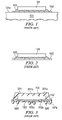
- FIG. 1 is a schematic cross section of a substrate with an assembled semiconductor chip resting on a chuck with planar surface, in known technology.
- FIG. 2 is a schematic cross section of an assembled device in known technology.
- FIG. 3 shows a schematic cross section of a finished device with polymerized molding compound and a plurality of solder balls, in known technology.
- FIG. 4 is a microphotograph of a cross section of an actual large-chip semiconductor device after polymerization of the molding compound in known technology.
- FIG. 5A is a schematic cross section of an example of a substrate with an assembled semiconductor chip resting on a chuck with a surface contour according to the invention.
- FIG. 5B is a schematic cross section of another example of a substrate with an assembled semiconductor chip resting on a chuck with a surface contour according to the invention.
- FIG. 6 is a schematic cross section of an assembled device, after the device has been assembled on a vacuum chuck according to the invention.
- FIG. 7 shows a schematic cross section of a finished device with polymerized molding compound and a plurality of solder balls, after the device has been assembled on a vacuum chuck according to the invention.
- FIG. 8 is a microphotograph of a cross section of an actual large-chip semiconductor device after assembly on a vacuum chuck according to the invention and after polymerization of the molding compound.
- FIG. 1 illustrates schematically a heatable chuck 101 , which has a planar, flat surface 101 a .
- surface 101 a are a plurality of openings (not shown in FIG. 1 ), through which a vacuum can be applied so that it sucks an object on surface 101 a to hold it tight against the surface.
- a substrate 102 is placed on surface 101 a; the substrate is also flat. Then the vacuum is turned on and substrate 102 is held tight against surface 101 a .
- a pre-determined amount of viscous adhesive material 103 (usually polyimide or epoxy) is deposited on substrate 102 (usually by a syringe).
- a semiconductor chip 104 is slightly pressed against attach material 103 and the material is partially polymerized by the thermal energy of the chuck. Chip 104 and substrate 102 are coplanar.
- the substrate 102 When the assembled chip and substrate are lifted from the chuck (see FIG. 2 ), the substrate 102 still has its planar configuration; it is still coplanar to chip 104 .
- thermoset polymer compound 301 usually molding compound.
- compound 301 is polymerized by storing the device at elevated temperatures for several hours. During the polymerization process, compound 301 undergoes a volumetric shrinkage. As a result, the finished device acquires a shape as schematically indicated in FIG. 3 : Substrate 102 is pulled towards the polymer compound and becomes curved outward (concave) under the chip 104 . Substrate 102 is no longer coplanar with chip 104 . Attach material 103 ends up thicker ( 301 b ) in the center of chip 104 compared to its thickness under the chip edges ( 301 a ). And the polymerized encapsulation material may have an outer surface 301 a , which not planar, but exhibits a slight dip 301 b in the center.
- solder balls 320 When solder balls 320 are attached to the outer surface 102 a of substrate 102 and the balls are of equal size, the plane of the balls cannot be coplanar with chip 104 .
- the solder When a device as depicted in FIG. 3 is to be attached to a circuit board, the solder is molten. Whenever the lack of coplanarity is so pronounced that it cannot be compensated by the reflowing solder, failures in board attach will occur.
- Chip 404 has a thickness 404 a of 275 ⁇ m and a length 404 b of 5.75 mm.
- the chip attach material 403 has a thickness 403 b of about 108 ⁇ m in the center, but only a thickness 403 a of approximately 87 ⁇ m at the chip edges; the difference between center and periphery is about 21 ⁇ m.
- the substrate 402 in FIG. 4 follows the curved outline of the chip attach material 403 .
- the following parts of the substrate are visible:
- the intermittent white-and-black layer 402 a consists of the copper traces separated by the solder mask;
- the grey layer 402 b is the polyimide tape.
- the whitish spheres are the solder balls 420 .
- the plurality of solder balls is not coplanar with the chip. (Finer detail of the substrate such as solder mask, nickel layer, etc. is not shown in FIG. 4 ).
- FIG. 5A depicts an assembly apparatus modified according to the invention.
- the heatable chuck 501 has a surface suitable for placing sheet-like substrates.
- the surface has openings for vacuum suction (not shown in FIG. 5A ).
- the chuck surface has area portions 502 a in a first plane and at least one area portion 502 b in a second plane elevated relative to the first plane so that the summary contour of the chuck surface becomes convex.
- An originally flat sheet-like substrate 503 when placed on the chuck surface and pulled towards the surface by the activated vacuum, will follow the summary convex contour and adopt this contour, as illustrated in FIG. 5A .
- the height difference 510 between surface 502 a and 502 b in FIG. 5A may be 25 ⁇ m for devices such as the ⁇ StarTM BGA. In other embodiments, the height difference may be larger of smaller. In yet other, more expensive embodiments, the whole surface of chuck 501 is smoothly micro-machined to obtain a continuously convex contour. The degree of convexity of the chuck surface is dependent on the material of the substrate, the area of the substrate, and the amount, composition, and polymerization of the encapsulation compound.
- a pre-determined amount of viscous adhesive material 504 (usually polyimide or epoxy) is deposited on substrate 503 (usually by a syringe).
- a semiconductor chip 505 is slightly pressed against attach material 504 and the material is partially polymerized by the thermal energy of the chuck.
- the thickness of the attach material 504 is distributed so that the thickness 504 b in the central area (under the chip) is smaller than the material thickness 504 a in the peripheral areas of the chip.
- the central material thickness 504 b may be left up to (but will not be larger than) the peripheral thickness 504 a.
- the considerations described above are preferably realized for relatively hard substrates, which operate in the plastic regime of the stress-strain relationship.
- the substrate behavior on the chuck 520 with the raised surface center looks schematically as shown in FIG. 5B .
- the height difference 530 between surface 522 a and 522 b is 25 ⁇ m. While the summary contour of the chuck surface is again convex, the originally flat sheet-like substrate 523 , when placed on the chuck surface and pulled towards the surface by the activated vacuum, will follow the actual surface contour more closely and adopt a more wavy profile as illustrated in FIG. 5B .
- a pre-determined amount of viscous adhesive material 524 (usually polyimide or epoxy) is deposited on substrate 523 (usually by a syringe).
- a semiconductor chip 525 is slightly pressed against attach material 524 and the material is partially polymerized by the thermal energy of the chuck.
- the thickness of the attach material 524 is distributed so that the thickness 524 b in the central area (under the chip) is smaller than the material thickness 524 a in the peripheral areas of the chip.
- the central material thickness 524 b may be left up to (but will not be larger than) the peripheral thickness 524 a.
- FIG. 6 illustrates, when the assembled chip and substrate are lifted from the chuck, the substrate 503 still retains its convex configuration.
- the thickness of the attach material 504 is distributed so that the thickness 504 b under the central area of the chip 505 is smaller than (or up to equal to) the material thickness 504 a under the peripheral areas of the chip.
- FIG. 7 The next process steps are summarized in FIG. 7 .
- FIG. 7 describes the effect of the encapsulation of the assembly in thermoset polymer compound 701 , preferably a molding compound. Because of the thermoset nature, compound 701 has to be polymerized after the encapsulation, preferably by storing the device at elevated temperatures for several hours. During the polymerization process, compound 701 undergoes a volumetric shrinkage. As a result, the finished device acquires a shape as schematically indicated in FIG. 7 : Substrate 503 is pulled towards the polymer compound and becomes planar under the chip 505 . Attach material 504 ends up with a thickness distribution so that the material thickness 504 b under the central chip area is equal to (or still slightly smaller than) the material thickness 504 a under the peripheral chip areas. Consequently, substrate 503 is now coplanar with chip 505 .
- the polymerized encapsulation material 701 has an outer surface 701 a , which is also coplanar with chip 505 .
- solder balls 720 are attached to the outer surface of substrate 503 and the balls are of equal size, the plane of the balls is coplanar with chip 505 .
- the solder is molten and there will be no failures in board attach.
- Chip 804 has a thickness 804 a of 275 ⁇ m and a length 804 b of 5.75 mm.
- the chip attach material 803 has an approximately uniform thickness 803 a of about 95 ⁇ m throughout its length. More precisely, the difference between the thickness in the center of 94 ⁇ m and the thickness at the periphery between 91 and 99 ⁇ m has reduced the difference to 10 ⁇ m.
- the substrate 802 in FIG. 8 follows the planar outline of the chip attach material 803 (for an explanation of the photograph detail visible in FIG. 8 see description under FIG. 4 ).
- the whitish spheres are the solder balls 820 .
- the plurality of solder balls is coplanar with the chip 804 .
Landscapes
- Engineering & Computer Science (AREA)
- Computer Hardware Design (AREA)
- Microelectronics & Electronic Packaging (AREA)
- Power Engineering (AREA)
- Manufacturing & Machinery (AREA)
- Physics & Mathematics (AREA)
- Condensed Matter Physics & Semiconductors (AREA)
- General Physics & Mathematics (AREA)
- Wire Bonding (AREA)
Abstract
A semiconductor device with a chip (505), its position defining a plane, and an insulating substrate (503) with first and second surfaces; the substrate is substantially coplanar with the chip, without warpage. One of the chip sides is attached to the first substrate surface using adhesive material (504), which has a thickness. The thickness of the adhesive material is distributed so that the thickness (504 b) under the central chip area is equal to or smaller than the material thickness (504 a) under the peripheral chip areas. Encapsulation compound (701) is embedding all remaining chip sides and the portions of the first substrate surface, which are not involved in the chip attachment. When reflow elements (720) are attached to the substrate contact pads, they are substantially coplanar with the chip.
Description
This application is a division of application Ser. No. 11/253,940 filed Oct. 19, 2005, now U.S. Pat. No. 7,244,638.
The present invention is related in general to the field of semiconductor devices and processes and more specifically to the structure and method of semiconductor chip attach in the device assembly process.
Any user of semiconductor components, who has the task of assembling components on electronic boards, can describe the aggravation encountered when just a single component lacks sufficient coplanarity for the board assembly. To avoid the difficulties, stringent requirements have often been established. As an example, for semiconductor devices with surface mount leads, the requirements included a coplanarity of about 0.14 mm for a lead pitch of 1 mm, and a coplanarity of about 0.05 mm for a lead pitch of 0.3 mm. The requirements increased rapidly with shrinking lead pitch.
For devices with solder balls, such as ball grid arrays (BGAs), insufficient coplanarity is manifested by a minority of solder balls not touching the substrate concurrently with the majority of balls. Consequently, efforts have been undertaken in literature to correct the coplanarity problems with solder balls of unequal size or delayed-reflow solder pastes. These efforts brought only limited success.
Applicants recognize the fact that, in BGAs, coplanarity problems are in most cases caused by device warpage and, consequently, an improvement of coplanarity should most readily be based on a reduction or elimination of device warpage. This approach is an inherently low-cost and robust methodology, since it eliminates coplanarity problems at the root cause. In addition, the approach is applicable to many device types and product families, and can be fine-tuned to a wide variety of materials characteristics of the substrates.
One embodiment of the invention is a semiconductor device with a chip, its position defining a plane, and an insulating substrate with first and second surfaces; the substrate is substantially coplanar with the chip, without warpage. One of the chip sides is attached to the first substrate surface using adhesive material, which has a thickness. The thickness of the adhesive material is distributed so that the thickness under the central chip area is equal to or smaller than the material thickness under the peripheral chip areas. Encapsulation compound is embedding all remaining chip sides and the portions of the first substrate surface, which are not involved in the chip attachment.
When a plurality of conductive contact pads are distributed over at least portions of the second substrate surface and a reflow element attached to each contact pad, this plurality of reflow elements is substantially coplanar with the chip.
Another embodiment of the invention is a method for fabricating a semiconductor device. An insulating substrate with first and second surfaces is provided. The second surface is placed on a chuck with openings for vacuum suction; the surface of the chuck is effectively convex, often practically achieved by a raised middle portion. The vacuum suction is activated so that the substrate is bent practically convex over the chuck surface. Adhesive material is then placed on the first substrate surface; the material is viscous and has a thickness. Next, a semiconductor chip is provided, which has sides, wherein one of the sides is intended for mechanical attachment. This attachment chip side is placed on the adhesive material; the thickness of the material becomes thereby distributed so that the thickness under the central area of the chip side is smaller than or equal to the material thickness under the peripheral areas of the chip side; the position of the chip defines a plane.
The vacuum suction is then de-activated and the substrate is removed from the chuck together with the assembled chip. All remaining chip surfaces and the portions of the first substrate surface not involved in the chip attachment are embedded in a thermoset encapsulation compound. The compound is polymerized, causing volumetric compound shrinkage, which pulls the substrate into a position substantially coplanar with the chip. The device does not exhibit warpage.
When the substrate is provided with a plurality of conductive contact pads distributed over at least portions of the second substrate surface, a reflow element can be attached to each contact pad; the plurality of reflow elements are then substantially coplanar with the substrate and the chip.
The technical advantages represented by certain embodiments of the invention will become apparent from the following description of the preferred embodiments of the invention, when considered in conjunction with the accompanying drawings and the novel features set forth in the appended claims.
Before the vacuum is turned on, a substrate 102 is placed on surface 101 a; the substrate is also flat. Then the vacuum is turned on and substrate 102 is held tight against surface 101 a. A pre-determined amount of viscous adhesive material 103 (usually polyimide or epoxy) is deposited on substrate 102 (usually by a syringe). A semiconductor chip 104 is slightly pressed against attach material 103 and the material is partially polymerized by the thermal energy of the chuck. Chip 104 and substrate 102 are coplanar.
When the assembled chip and substrate are lifted from the chuck (see FIG. 2 ), the substrate 102 still has its planar configuration; it is still coplanar to chip 104.
The assembly is then encapsulated in thermoset polymer compound 301, usually molding compound. After the encapsulation, compound 301 is polymerized by storing the device at elevated temperatures for several hours. During the polymerization process, compound 301 undergoes a volumetric shrinkage. As a result, the finished device acquires a shape as schematically indicated in FIG. 3 : Substrate 102 is pulled towards the polymer compound and becomes curved outward (concave) under the chip 104. Substrate 102 is no longer coplanar with chip 104. Attach material 103 ends up thicker (301 b) in the center of chip 104 compared to its thickness under the chip edges (301 a). And the polymerized encapsulation material may have an outer surface 301 a, which not planar, but exhibits a slight dip 301 b in the center.
When solder balls 320 are attached to the outer surface 102 a of substrate 102 and the balls are of equal size, the plane of the balls cannot be coplanar with chip 104. When a device as depicted in FIG. 3 is to be attached to a circuit board, the solder is molten. Whenever the lack of coplanarity is so pronounced that it cannot be compensated by the reflowing solder, failures in board attach will occur.
The microphotograph in FIG. 4 of a cross section of an actual device encapsulated by molding material 401 and assembled on a chuck with planar surface illustrates the unequal thickness of the attach material. Chip 404 has a thickness 404 a of 275 μm and a length 404 b of 5.75 mm. The chip attach material 403 has a thickness 403 b of about 108 μm in the center, but only a thickness 403 a of approximately 87 μm at the chip edges; the difference between center and periphery is about 21 μm.
As the microphotograph shows, the substrate 402 in FIG. 4 follows the curved outline of the chip attach material 403. The following parts of the substrate are visible: The intermittent white-and-black layer 402 a consists of the copper traces separated by the solder mask; the grey layer 402 b is the polyimide tape. The whitish spheres are the solder balls 420. The plurality of solder balls is not coplanar with the chip. (Finer detail of the substrate such as solder mask, nickel layer, etc. is not shown in FIG. 4 ).
The embodiment of FIG. 5A depicts an assembly apparatus modified according to the invention. The heatable chuck 501 has a surface suitable for placing sheet-like substrates. The surface has openings for vacuum suction (not shown in FIG. 5A ). The chuck surface has area portions 502 a in a first plane and at least one area portion 502 b in a second plane elevated relative to the first plane so that the summary contour of the chuck surface becomes convex. An originally flat sheet-like substrate 503, when placed on the chuck surface and pulled towards the surface by the activated vacuum, will follow the summary convex contour and adopt this contour, as illustrated in FIG. 5A .
As an example, the height difference 510 between surface 502 a and 502 b in FIG. 5A may be 25 μm for devices such as the μStar™ BGA. In other embodiments, the height difference may be larger of smaller. In yet other, more expensive embodiments, the whole surface of chuck 501 is smoothly micro-machined to obtain a continuously convex contour. The degree of convexity of the chuck surface is dependent on the material of the substrate, the area of the substrate, and the amount, composition, and polymerization of the encapsulation compound.
In the next process step, a pre-determined amount of viscous adhesive material 504 (usually polyimide or epoxy) is deposited on substrate 503 (usually by a syringe). A semiconductor chip 505 is slightly pressed against attach material 504 and the material is partially polymerized by the thermal energy of the chuck.
As a result of the convex substrate shape, the thickness of the attach material 504 is distributed so that the thickness 504 b in the central area (under the chip) is smaller than the material thickness 504 a in the peripheral areas of the chip. When a different height 510 of the central chuck surface is selected, the central material thickness 504 b may be left up to (but will not be larger than) the peripheral thickness 504 a.
The considerations described above are preferably realized for relatively hard substrates, which operate in the plastic regime of the stress-strain relationship. For softer substrates operating in the plastic regime, the substrate behavior on the chuck 520 with the raised surface center looks schematically as shown in FIG. 5B . The height difference 530 between surface 522 a and 522 b is 25 μm. While the summary contour of the chuck surface is again convex, the originally flat sheet-like substrate 523, when placed on the chuck surface and pulled towards the surface by the activated vacuum, will follow the actual surface contour more closely and adopt a more wavy profile as illustrated in FIG. 5B .
In the next process step, a pre-determined amount of viscous adhesive material 524 (usually polyimide or epoxy) is deposited on substrate 523 (usually by a syringe). A semiconductor chip 525 is slightly pressed against attach material 524 and the material is partially polymerized by the thermal energy of the chuck.
As a result of the wavy convex substrate shape, the thickness of the attach material 524 is distributed so that the thickness 524 b in the central area (under the chip) is smaller than the material thickness 524 a in the peripheral areas of the chip. When a different height 530 of the central chuck surface is selected, the central material thickness 524 b may be left up to (but will not be larger than) the peripheral thickness 524 a.
As FIG. 6 illustrates, when the assembled chip and substrate are lifted from the chuck, the substrate 503 still retains its convex configuration. The thickness of the attach material 504 is distributed so that the thickness 504 b under the central area of the chip 505 is smaller than (or up to equal to) the material thickness 504 a under the peripheral areas of the chip. The next process steps are summarized in FIG. 7 .
When solder balls 720 are attached to the outer surface of substrate 503 and the balls are of equal size, the plane of the balls is coplanar with chip 505. When a device as depicted in FIG. 7 is to be attached to a circuit board, the solder is molten and there will be no failures in board attach.
The microphotograph in FIG. 8 of a cross section of an actual device, assembled on a chuck with effectively convex surface and encapsulated by molding material 801, illustrates the equal thickness of the attach material 803. Chip 804 has a thickness 804 a of 275 μm and a length 804 b of 5.75 mm. The chip attach material 803 has an approximately uniform thickness 803 a of about 95 μm throughout its length. More precisely, the difference between the thickness in the center of 94 μm and the thickness at the periphery between 91 and 99 μm has reduced the difference to 10 μm.
As the microphotograph shows, the substrate 802 in FIG. 8 follows the planar outline of the chip attach material 803 (for an explanation of the photograph detail visible in FIG. 8 see description under FIG. 4 ). The whitish spheres are the solder balls 820. The plurality of solder balls is coplanar with the chip 804.
Statistical data collected from many manufacturing lots about coplanarity and board assembly have confirmed the reduced device warpage, improved solder ball coplanarity (at least 26%) and improved board attach reliability based on the effectively convex assembly chuck according to the invention. The only significant reliability factor left was related to solder ball variability.
While this invention has been described in reference to illustrative embodiments, this description is not intended to be construed in a limiting sense. Various modifications and combinations of the illustrative embodiments, as well as other embodiments of the invention, will be apparent to persons skilled in the art upon reference to the description. As an example, more than one raised center of the assembly chuck may be advisable for large area chips. As another example, for production with high throughput the cost of a micro-machined concave chuck surface may be justified; if would enhance the precision of the attach material thickness uniformity. It is therefore intended that the appended claims encompass any such modifications.
Claims (7)
1. A semiconductor device comprising:
a semiconductor chip, its position defining a plane;
an insulating substrate having first and second surfaces, the substrate substantially coplanar with the chip;
one of the chip sides attached to the first substrate surface using adhesive material, the material having a thickness;
the adhesive material thickness distributed so that the thickness under the central chip area is smaller than the material thickness under the peripheral chip areas; and
encapsulation compound embedding all remaining chip sides and the portions of the first substrate surface not involved in the chip attachment.
2. The device according to claim 1 further comprising a plurality of conductive contact pads distributed over at least portions of the second substrate surface, the contact pads suitable for the attachment of reflow elements.
3. The device according to claim 2 further having a reflow element attached to each contact pad, the plurality of reflow elements being substantially coplanar with the substrate and the chip.
4. The device according to claim 1 wherein the substrate includes a soft insulator.
5. The device according to claim 1 wherein the substrate includes a hard insulator.
6. The device according to claim 1 wherein the adhesive material is a polymer including polyimides and epoxies.
7. The device according to claim 1 wherein the encapsulation compound is a thermoset polymer including epoxy, which is polymerized.
Priority Applications (1)
| Application Number | Priority Date | Filing Date | Title |
|---|---|---|---|
| US11/762,186 US7462943B2 (en) | 2005-10-19 | 2007-06-13 | Semiconductor assembly for improved device warpage and solder ball coplanarity |
Applications Claiming Priority (2)
| Application Number | Priority Date | Filing Date | Title |
|---|---|---|---|
| US11/253,940 US7244636B2 (en) | 2005-10-19 | 2005-10-19 | Semiconductor assembly for improved device warpage and solder ball coplanarity |
| US11/762,186 US7462943B2 (en) | 2005-10-19 | 2007-06-13 | Semiconductor assembly for improved device warpage and solder ball coplanarity |
Related Parent Applications (1)
| Application Number | Title | Priority Date | Filing Date |
|---|---|---|---|
| US11/253,940 Division US7244636B2 (en) | 2005-10-19 | 2005-10-19 | Semiconductor assembly for improved device warpage and solder ball coplanarity |
Publications (2)
| Publication Number | Publication Date |
|---|---|
| US20080142949A1 US20080142949A1 (en) | 2008-06-19 |
| US7462943B2 true US7462943B2 (en) | 2008-12-09 |
Family
ID=37947385
Family Applications (2)
| Application Number | Title | Priority Date | Filing Date |
|---|---|---|---|
| US11/253,940 Active 2026-01-14 US7244636B2 (en) | 2005-10-19 | 2005-10-19 | Semiconductor assembly for improved device warpage and solder ball coplanarity |
| US11/762,186 Active US7462943B2 (en) | 2005-10-19 | 2007-06-13 | Semiconductor assembly for improved device warpage and solder ball coplanarity |
Family Applications Before (1)
| Application Number | Title | Priority Date | Filing Date |
|---|---|---|---|
| US11/253,940 Active 2026-01-14 US7244636B2 (en) | 2005-10-19 | 2005-10-19 | Semiconductor assembly for improved device warpage and solder ball coplanarity |
Country Status (6)
| Country | Link |
|---|---|
| US (2) | US7244636B2 (en) |
| EP (1) | EP1946373A4 (en) |
| KR (1) | KR20080080498A (en) |
| CN (1) | CN101410970A (en) |
| TW (1) | TW200731475A (en) |
| WO (1) | WO2007048090A2 (en) |
Cited By (1)
| Publication number | Priority date | Publication date | Assignee | Title |
|---|---|---|---|---|
| US20090250810A1 (en) * | 2008-04-07 | 2009-10-08 | Pendse Rajendra D | Integrated circuit packaging system with warpage control system and method of manufacture thereof |
Families Citing this family (4)
| Publication number | Priority date | Publication date | Assignee | Title |
|---|---|---|---|---|
| TWI407512B (en) * | 2010-06-14 | 2013-09-01 | Advanced Semiconductor Eng | Semiconductor package and manufacturing method thereof |
| US9896330B2 (en) * | 2016-01-13 | 2018-02-20 | Texas Instruments Incorporated | Structure and method for packaging stress-sensitive micro-electro-mechanical system stacked onto electronic circuit chip |
| US10879144B2 (en) | 2018-08-14 | 2020-12-29 | Texas Instruments Incorporated | Semiconductor package with multilayer mold |
| US11742266B2 (en) | 2019-12-12 | 2023-08-29 | Texas Instruments Incorporated | Electronic device topside cooling |
Citations (9)
| Publication number | Priority date | Publication date | Assignee | Title |
|---|---|---|---|---|
| US5252850A (en) | 1992-01-27 | 1993-10-12 | Photometrics Ltd. | Apparatus for contouring a semiconductor, light responsive array with a prescribed physical profile |
| US5509464A (en) | 1993-07-30 | 1996-04-23 | Applied Materials, Inc. | Method and apparatus for cooling rectangular substrates |
| US20010005602A1 (en) | 1999-12-24 | 2001-06-28 | Kabushiki Kaisha Shinkawa | Multi-chip bonding method and apparatus |
| US6392143B1 (en) | 1999-01-18 | 2002-05-21 | Kabushiki Kaisha Toshiba | Flexible package having very thin semiconductor chip, module and multi chip module (MCM) assembled by the package, and method for manufacturing the same |
| US20020090759A1 (en) | 1998-09-30 | 2002-07-11 | Nobuaki Hashimoto | Semiconductor device, method of connecting a semiconductor chip, circuit board, and electronic equipment |
| US6446948B1 (en) | 2000-03-27 | 2002-09-10 | International Business Machines Corporation | Vacuum chuck for reducing distortion of semiconductor and GMR head wafers during processing |
| US20030052419A1 (en) | 2001-09-18 | 2003-03-20 | Hitachi, Ltd. | Semiconductor device and method of manufacturing the same |
| US20030170444A1 (en) | 2002-03-05 | 2003-09-11 | Stewart Steven L. | Attachment of surface mount devices to printed circuit boards using a thermoplastic adhesive |
| US7148081B2 (en) * | 2003-05-30 | 2006-12-12 | Renesas Technology Corp. | Method of manufacturing a semiconductor device |
Family Cites Families (6)
| Publication number | Priority date | Publication date | Assignee | Title |
|---|---|---|---|---|
| JPS5655057A (en) * | 1979-10-12 | 1981-05-15 | Fujitsu Ltd | Manufacture of semiconductor device |
| JPH0766092A (en) * | 1993-08-23 | 1995-03-10 | Sumitomo Sitix Corp | Method for adhering semiconductor wafer and adhering jig |
| JPH10326800A (en) * | 1997-05-26 | 1998-12-08 | Seiko Epson Corp | Manufacture of semiconductor device and mold for semiconductor manufacturing device |
| DE10126508B4 (en) * | 2001-05-30 | 2008-11-13 | Infineon Technologies Ag | Device with electronic components packaged by means of injection molding technology, injection molding tool and method for packaging electronic components |
| JP3971314B2 (en) | 2003-01-29 | 2007-09-05 | シャープ株式会社 | Semiconductor manufacturing equipment |
| JP4461826B2 (en) | 2004-02-17 | 2010-05-12 | パナソニック株式会社 | Electronic component mounting equipment |
-
2005
- 2005-10-19 US US11/253,940 patent/US7244636B2/en active Active
-
2006
- 2006-10-17 KR KR1020087011773A patent/KR20080080498A/en not_active Application Discontinuation
- 2006-10-17 EP EP06839453A patent/EP1946373A4/en not_active Withdrawn
- 2006-10-17 WO PCT/US2006/060036 patent/WO2007048090A2/en active Application Filing
- 2006-10-17 CN CNA2006800389189A patent/CN101410970A/en active Pending
- 2006-10-19 TW TW095138599A patent/TW200731475A/en unknown
-
2007
- 2007-06-13 US US11/762,186 patent/US7462943B2/en active Active
Patent Citations (9)
| Publication number | Priority date | Publication date | Assignee | Title |
|---|---|---|---|---|
| US5252850A (en) | 1992-01-27 | 1993-10-12 | Photometrics Ltd. | Apparatus for contouring a semiconductor, light responsive array with a prescribed physical profile |
| US5509464A (en) | 1993-07-30 | 1996-04-23 | Applied Materials, Inc. | Method and apparatus for cooling rectangular substrates |
| US20020090759A1 (en) | 1998-09-30 | 2002-07-11 | Nobuaki Hashimoto | Semiconductor device, method of connecting a semiconductor chip, circuit board, and electronic equipment |
| US6392143B1 (en) | 1999-01-18 | 2002-05-21 | Kabushiki Kaisha Toshiba | Flexible package having very thin semiconductor chip, module and multi chip module (MCM) assembled by the package, and method for manufacturing the same |
| US20010005602A1 (en) | 1999-12-24 | 2001-06-28 | Kabushiki Kaisha Shinkawa | Multi-chip bonding method and apparatus |
| US6446948B1 (en) | 2000-03-27 | 2002-09-10 | International Business Machines Corporation | Vacuum chuck for reducing distortion of semiconductor and GMR head wafers during processing |
| US20030052419A1 (en) | 2001-09-18 | 2003-03-20 | Hitachi, Ltd. | Semiconductor device and method of manufacturing the same |
| US20030170444A1 (en) | 2002-03-05 | 2003-09-11 | Stewart Steven L. | Attachment of surface mount devices to printed circuit boards using a thermoplastic adhesive |
| US7148081B2 (en) * | 2003-05-30 | 2006-12-12 | Renesas Technology Corp. | Method of manufacturing a semiconductor device |
Cited By (2)
| Publication number | Priority date | Publication date | Assignee | Title |
|---|---|---|---|---|
| US20090250810A1 (en) * | 2008-04-07 | 2009-10-08 | Pendse Rajendra D | Integrated circuit packaging system with warpage control system and method of manufacture thereof |
| US8217514B2 (en) | 2008-04-07 | 2012-07-10 | Stats Chippac Ltd. | Integrated circuit packaging system with warpage control system and method of manufacture thereof |
Also Published As
| Publication number | Publication date |
|---|---|
| WO2007048090A3 (en) | 2008-11-20 |
| US7244636B2 (en) | 2007-07-17 |
| TW200731475A (en) | 2007-08-16 |
| US20080142949A1 (en) | 2008-06-19 |
| CN101410970A (en) | 2009-04-15 |
| EP1946373A2 (en) | 2008-07-23 |
| EP1946373A4 (en) | 2010-04-07 |
| US20070085171A1 (en) | 2007-04-19 |
| KR20080080498A (en) | 2008-09-04 |
| WO2007048090A2 (en) | 2007-04-26 |
Similar Documents
| Publication | Publication Date | Title |
|---|---|---|
| KR100551641B1 (en) | A method of manufacturing a semiconductor device and a semiconductor device | |
| EP1445995B1 (en) | Method of mounting an electronic component on a circuit board and system for carrying out the method | |
| US6722028B2 (en) | Method of making electronic device | |
| US20080099910A1 (en) | Flip-Chip Semiconductor Package with Encapsulant Retaining Structure and Strip | |
| US20070127224A1 (en) | Electronic circuit device and method of manufacturing the same | |
| US20030173679A1 (en) | Stacked dice standoffs | |
| US20070194456A1 (en) | Flexible circuit substrate for flip-chip-on-flex applications | |
| US10867952B2 (en) | Semiconductor structure and manufacturing method thereof | |
| US7462943B2 (en) | Semiconductor assembly for improved device warpage and solder ball coplanarity | |
| US8345444B2 (en) | Structure with electronic component mounted therein and method for manufacturing such structure | |
| US7647694B2 (en) | Method for mounting electronic component | |
| US6320249B1 (en) | Multiple line grids incorporating therein circuit elements | |
| US7661964B2 (en) | Connecting parts and multilayer wiring board | |
| US6492715B1 (en) | Integrated semiconductor package | |
| US20050189625A1 (en) | Lead-frame for electonic devices with extruded pads | |
| JP4436588B2 (en) | Semiconductor mounting module | |
| US12021004B2 (en) | Embedded lid for low cost and improved thermal performance | |
| KR200179419Y1 (en) | Semiconductor package | |
| JP2004259755A (en) | Method of manufacturing semiconductor device | |
| KR100367729B1 (en) | Multiple line grid array package | |
| KR100650492B1 (en) | Packaging structure of flipchip and packaging method thereof | |
| JP2009105350A (en) | Semiconductor apparatus and method of manufacturing the same | |
| JP2000091458A (en) | Semiconductor device and its manufacture | |
| JP2002026188A (en) | Manufacturing method for ball grid array semiconductor device | |
| JPH0621257U (en) | Surface Mounted Plastic Pinglit Array |
Legal Events
| Date | Code | Title | Description |
|---|---|---|---|
| STCF | Information on status: patent grant |
Free format text: PATENTED CASE |
|
| FPAY | Fee payment |
Year of fee payment: 4 |
|
| FPAY | Fee payment |
Year of fee payment: 8 |
|
| MAFP | Maintenance fee payment |
Free format text: PAYMENT OF MAINTENANCE FEE, 12TH YEAR, LARGE ENTITY (ORIGINAL EVENT CODE: M1553); ENTITY STATUS OF PATENT OWNER: LARGE ENTITY Year of fee payment: 12 |