US7315348B2 - Exposure apparatus, focal point detecting method, exposure method and device manufacturing method - Google Patents
Exposure apparatus, focal point detecting method, exposure method and device manufacturing method Download PDFInfo
- Publication number
- US7315348B2 US7315348B2 US11/110,735 US11073505A US7315348B2 US 7315348 B2 US7315348 B2 US 7315348B2 US 11073505 A US11073505 A US 11073505A US 7315348 B2 US7315348 B2 US 7315348B2
- Authority
- US
- United States
- Prior art keywords
- substrate
- stage
- original
- optical system
- reference member
- Prior art date
- Legal status (The legal status is an assumption and is not a legal conclusion. Google has not performed a legal analysis and makes no representation as to the accuracy of the status listed.)
- Expired - Fee Related, expires
Links
- 238000000034 method Methods 0.000 title claims description 50
- 238000004519 manufacturing process Methods 0.000 title claims description 13
- 230000003287 optical effect Effects 0.000 claims abstract description 224
- 239000000758 substrate Substances 0.000 claims abstract description 93
- 238000005286 illumination Methods 0.000 claims abstract description 62
- 238000001514 detection method Methods 0.000 claims description 8
- 230000008859 change Effects 0.000 claims description 6
- 238000012545 processing Methods 0.000 claims description 6
- 230000005855 radiation Effects 0.000 claims 1
- 238000005259 measurement Methods 0.000 description 42
- 239000004065 semiconductor Substances 0.000 description 13
- 238000012546 transfer Methods 0.000 description 7
- 230000008569 process Effects 0.000 description 5
- 230000009467 reduction Effects 0.000 description 5
- 230000007423 decrease Effects 0.000 description 3
- 238000011156 evaluation Methods 0.000 description 3
- 230000003247 decreasing effect Effects 0.000 description 2
- 238000011161 development Methods 0.000 description 2
- 238000005530 etching Methods 0.000 description 2
- 238000007689 inspection Methods 0.000 description 2
- 238000001459 lithography Methods 0.000 description 2
- 239000000463 material Substances 0.000 description 2
- 238000012360 testing method Methods 0.000 description 2
- 239000006096 absorbing agent Substances 0.000 description 1
- 230000015572 biosynthetic process Effects 0.000 description 1
- 239000003795 chemical substances by application Substances 0.000 description 1
- 238000007796 conventional method Methods 0.000 description 1
- 230000008021 deposition Effects 0.000 description 1
- 238000013461 design Methods 0.000 description 1
- 238000009826 distribution Methods 0.000 description 1
- 238000005538 encapsulation Methods 0.000 description 1
- 230000010354 integration Effects 0.000 description 1
- 238000005468 ion implantation Methods 0.000 description 1
- 150000002500 ions Chemical class 0.000 description 1
- QSHDDOUJBYECFT-UHFFFAOYSA-N mercury Chemical compound [Hg] QSHDDOUJBYECFT-UHFFFAOYSA-N 0.000 description 1
- 229910052753 mercury Inorganic materials 0.000 description 1
- 238000012986 modification Methods 0.000 description 1
- 230000004048 modification Effects 0.000 description 1
- 230000003647 oxidation Effects 0.000 description 1
- 238000007254 oxidation reaction Methods 0.000 description 1
- 238000004806 packaging method and process Methods 0.000 description 1
- 229910052710 silicon Inorganic materials 0.000 description 1
- 239000010703 silicon Substances 0.000 description 1
Images


Classifications
-
- G—PHYSICS
- G03—PHOTOGRAPHY; CINEMATOGRAPHY; ANALOGOUS TECHNIQUES USING WAVES OTHER THAN OPTICAL WAVES; ELECTROGRAPHY; HOLOGRAPHY
- G03B—APPARATUS OR ARRANGEMENTS FOR TAKING PHOTOGRAPHS OR FOR PROJECTING OR VIEWING THEM; APPARATUS OR ARRANGEMENTS EMPLOYING ANALOGOUS TECHNIQUES USING WAVES OTHER THAN OPTICAL WAVES; ACCESSORIES THEREFOR
- G03B27/00—Photographic printing apparatus
- G03B27/32—Projection printing apparatus, e.g. enlarger, copying camera
- G03B27/52—Details
-
- G—PHYSICS
- G03—PHOTOGRAPHY; CINEMATOGRAPHY; ANALOGOUS TECHNIQUES USING WAVES OTHER THAN OPTICAL WAVES; ELECTROGRAPHY; HOLOGRAPHY
- G03F—PHOTOMECHANICAL PRODUCTION OF TEXTURED OR PATTERNED SURFACES, e.g. FOR PRINTING, FOR PROCESSING OF SEMICONDUCTOR DEVICES; MATERIALS THEREFOR; ORIGINALS THEREFOR; APPARATUS SPECIALLY ADAPTED THEREFOR
- G03F9/00—Registration or positioning of originals, masks, frames, photographic sheets or textured or patterned surfaces, e.g. automatically
- G03F9/70—Registration or positioning of originals, masks, frames, photographic sheets or textured or patterned surfaces, e.g. automatically for microlithography
- G03F9/7003—Alignment type or strategy, e.g. leveling, global alignment
- G03F9/7023—Aligning or positioning in direction perpendicular to substrate surface
- G03F9/7026—Focusing
-
- G—PHYSICS
- G03—PHOTOGRAPHY; CINEMATOGRAPHY; ANALOGOUS TECHNIQUES USING WAVES OTHER THAN OPTICAL WAVES; ELECTROGRAPHY; HOLOGRAPHY
- G03F—PHOTOMECHANICAL PRODUCTION OF TEXTURED OR PATTERNED SURFACES, e.g. FOR PRINTING, FOR PROCESSING OF SEMICONDUCTOR DEVICES; MATERIALS THEREFOR; ORIGINALS THEREFOR; APPARATUS SPECIALLY ADAPTED THEREFOR
- G03F9/00—Registration or positioning of originals, masks, frames, photographic sheets or textured or patterned surfaces, e.g. automatically
- G03F9/70—Registration or positioning of originals, masks, frames, photographic sheets or textured or patterned surfaces, e.g. automatically for microlithography
- G03F9/7088—Alignment mark detection, e.g. TTR, TTL, off-axis detection, array detector, video detection
Definitions
- the present invention relates to an exposure apparatus, a focal point detecting method, an exposure method, and a device manufacturing method and, more particularly, to an exposure apparatus, which projects and transfers a pattern of a reflective original onto a substrate, a focal point detecting method to be applied to the exposure apparatus, an exposure method to be applied to the exposure apparatus and a device manufacturing method using the exposure method.
- the wafer is positioned on the focus (focal point) of the projection optical system by adjusting the positional relationship between the projection optical system and a reference member provided to a wafer stage which supports the wafer.
- the reticle is positioned on the focus of the projection optical system by adjusting the positional relationship between the projection optical system and a reference member on a reticle stage which holds the reticle.
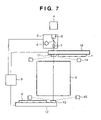
- a first conventional example of a method of detecting the focal point of a projection optical system with respect to a reference member on a wafer stage will be described.
- a transmissive reticle 1 is illuminated by an illumination optical system 4 , and the pattern of the reticle 1 is projected onto a resist-applied wafer 2 by a projection optical system 3 .
- An evaluating unit 5 illuminates a focus mark which is formed on a reference member 13 on a wafer stage 12 with measuring light through a projection optical system 3 , and evaluates it.
- the evaluating unit 5 has an illumination unit 6 , a focal point changing unit 7 which changes the focal point of the evaluating unit 5 by a relay lens or the like, a photo-receiving unit 8 such as an image sensor, and the like.
- a reticle stage 10 can move in a three-dimensional direction while holding the reticle 1 , and is provided with a reference member 11 having a reflecting surface.
- a wafer stage 12 can move in the three-directional direction while holding the wafer 2 , and is provided with the reference member 13 having the focus mark.
- a reticle stage height detector 14 measures the position (i.e., the height) of the reticle stage 10 in the direction of the optical axis of the projection optical system 3 .
- a detector 15 which detects the height of the wafer stage 12 measures the position (i.e., the height) of the wafer stage 12 in the direction of the optical axis of the projection optical system 3 .
- a controller 9 controls the operation of the exposure apparatus. For example, the controller 9 controls the positions of the reticle stage 10 and wafer stage 12 , and detects the focal point of the projection optical system 3 while controlling the reticle stage 10 , wafer stage 12 , and evaluating unit 5 .
- the exposure apparatus detects the focal point of the projection optical system 3 with respect to the reference member 13 on the wafer stage 12 in accordance with a procedure to be described later to move the wafer stage 12 to the focal point of the projection optical system 3 .
- the exposure apparatus moves the reticle stage reference member 11 to the focal point of the illumination optical system 4 which is measured or adjusted in advance by using the reticle stage height detector 14 , illuminates the pattern on the reticle 1 with illumination light from the illumination optical system 4 , and projects and transfers the pattern onto the reticle 1 through the projection optical system 3 .
- the exposure apparatus has an alignment measurement unit (not shown) to align the reticle 1 and wafer 2 relative to each other in a direction perpendicular to the optical axis of the projection optical system 3 as well.
- a contrast indicating the light quantity distribution of the focus mark on the wafer stage 12 is measured at a plurality of portions, to obtain the reticle stage position (axis of abscissa) and the contrast (axis of ordinate) obtained then, as shown in FIG. 4 .
- the focal point of the projection optical system 3 with respect to the wafer stage 12 is calculated on the basis of the position of the reticle stage 10 at which the contrast becomes the maximum.
- the reticle stage 10 When the reticle stage 10 is moved along the optical axis of the projection optical system 3 , the reticle stage 10 is undesirably shifted from the focal point of the evaluating unit 5 . Hence, the focal point of the evaluating unit 5 is changed by using the focal point changing unit 7 in the evaluating unit 5 , so that the focal point of the evaluating unit 5 can be aligned with the position of the reticle stage 10 .
- FIG. 9 shows an example of the focus mark on the wafer stage 12 .
- the contrast of the mark image of FIG. 9 becomes the maximum.
- the contrast decreases.
- the photo-receiving unit 8 includes an image sensor
- the light quantity change amount in the directions (broken lines A and B in FIG. 9 ) of the short sides of respective rectangles in a mark image sensed by the photo-receiving unit 8 is calculated as the sum of the difference values between adjacent pixels, thereby measuring the contrast.
- the focal point of the projection optical system 3 with respect to the reference member 13 on the wafer stage 12 can be specifically detected in accordance with the procedure shown in FIG. 8 .
- Original driving step S 201 the reticle stage 10 is moved along the optical axis of the projection optical system 3 .
- measured focal point changing step S 202 the focal point of the evaluating unit 5 is aligned with the reference member 11 provided to the reticle stage 10 by using the focal point changing unit 7 in the evaluating unit 5 .
- the focus mark image on the wafer stage 12 is sensed by using the evaluating unit 5 , and the contrast of the sensed mark image is calculated by an arithmetic operation unit.
- focal point calculating step S 204 the focal point of the projection optical system 3 is calculated by the method, which is described above with reference to FIG. 4 .
- the positions of the reticle stage 10 and wafer stage 12 in the direction of the optical axis of the projection optical system 3 can be measured by using the reticle stage height detector 14 and wafer stage height detector 15 , and controlled by the controller 9 on the basis of the measurement results.
- the above method is to calculate the focal point of the projection optical system 3 with respect to the reference member 13 while changing the position of the reticle stage 10 in the direction of the optical axis of the projection optical system 3 .
- the focal point of the projection optical system 3 with respect to the reference member 13 can also be calculated by measuring the contrast of the mark image while changing the position of the wafer stage 12 in the direction of the optical axis of the projection optical system 3 .
- a contrast change, which occurs when the position of the reticle stage 10 is changed, is more moderate than a contrast change, which occurs when the position of the wafer stage 12 is changed by the square of the reduction ratio of the projection optical system 3 .
- the former method is advantageous in that it is less influenced by an error in position of the stage, which is measured by the optical axis method of the projection optical system 3 .
- the reduction ratio of a projection optical system used in an exposure apparatus is 1/4 or 1/5.
- the influence of an error in position of the stage is accordingly, 1/16 or 1/25.
- a transmissive reticle 1 is illuminated by an illumination optical system 4 , and the pattern of the reticle 1 is projected onto a resist-applied wafer 2 by a projection optical system 3 .
- a measurement illumination unit 16 illuminates a focus mark which is formed on a reticle stage 10 and furthermore a focus mark formed on a wafer stage 12 through the projection optical system 3 with measuring light.
- the measurement illumination unit 16 has an illumination unit 6 and a focal point changing unit 7 which changes the focal point of the measurement illumination unit 16 by a relay lens or the like.
- the reticle stage 10 can move in a three-dimensional direction while holding the reticle 1 , and is provided with a reference member 11 having the slit-shaped focus mark.
- the wafer stage 12 can move in the three-directional direction while holding the wafer 2 , and is provided with a reference member 13 having a slit-shaped mark and a photo-receiving unit 8 , e.g., a light quantity sensor, which is arranged under the reference member 13 .
- a controller 9 controls the operation of the exposure apparatus. For example, the controller 9 controls the positions of the reticle stage 10 and wafer stage 12 , and detects the focal point of the projection optical system 3 while controlling the reticle stage 10 , wafer stage 12 , and measurement illumination unit 16 .
- the measurement illumination unit 16 and the photo-receiving unit 8 on the wafer stage 12 form an evaluating unit.
- a reticle stage height detector 14 measures the position (i.e., the height) of the reticle stage 10 in the direction of the optical axis of the projection optical system 3 .
- a wafer stage height detector 15 measures the position (i.e., the height) of the wafer stage 12 in the direction of the optical axis of the projection optical system 3 .
- the focus marks on the reference members 11 and 13 on the reticle stage 10 and wafer stage 12 have shapes shown in FIGS. 11A and 11B , respectively.
- the focus marks are used for detecting the focal point of the projection optical system 3 after their positions are aligned relative to each other in a direction perpendicular to the optical axis of the projection optical system 3 .
- the light quantity of the measuring light which is to be received by the photo-receiving unit 8 , from the measurement illumination unit 16 , becomes the maximum.
- the outline of the operation of the exposure apparatus shown in FIG. 10 is identical to that of the first conventional example and a description thereof will, accordingly, be omitted.
- the measuring light passing through the focus marks on the reticle stage 10 and wafer stage 12 is received by the photo-receiving unit 8 , and its light quantity is measured to obtain the reticle stage position (axis of abscissa) and the light quantity (axis of ordinate) as shown in FIG. 6 .
- the focal point of the projection optical system 3 with respect to the wafer stage 12 is calculated on the basis of the position of the reticle stage 10 at which the light quantity becomes the maximum.
- the reticle stage 10 When the reticle stage 10 is moved along the optical axis of the projection optical system 3 , the reticle stage 10 is undesirably shifted from the focal point of the measurement illumination unit 16 . Hence, the focal point of the measurement illumination unit 16 is changed by using the focal point changing unit 7 in the measurement illumination unit 16 , so that the focal point of the measurement illumination unit 16 can be aligned with the position of the reticle stage 10 .
- the focal point of the projection optical system 3 can be detected in accordance with the procedure shown in FIG. 8 in the same manner as that in the first conventional example.
- Original driving step S 201 the reticle stage 10 is moved along the optical axis of the projection optical system 3 .
- measured focal point changing step S 202 the focal point of the measurement illumination unit 16 is aligned with the reference member 11 provided to the reticle stage 10 by using the focal point changing unit 7 in the measurement illumination unit 16 .
- light quantity measuring step S 203 the light quantity of the illumination light from the measurement illumination unit 16 is measured by using the photo-receiving unit 8 provided to the wafer stage 12 .
- focal point calculating step S 204 the focal point of the projection optical system 3 is calculated by the method, which is described above with reference to FIG. 6 .
- the positions of the reticle stage 10 and wafer stage 12 in the direction of the optical axis of the projection optical system 3 can be measured by using the reticle stage height detector 14 and wafer stage height detector 15 , and controlled by the controller 9 on the basis of the measurement results.
- the second conventional method is to calculate the focal point of the projection optical system 3 with respect to the reference member 13 while changing the position of the reticle stage 10 in the direction of the optical axis of the projection optical system 3 , in the same manner as in the first conventional example.
- the focal point of the projection optical system 3 with respect to the reference member 13 can also be calculated by measuring the illumination light quantity while changing the position of the wafer stage 12 in the direction of the optical axis of the projection optical system 3 , in the same manner as in the first conventional example. Due to the same reason as in the first conventional example, the former method is advantageous in that it is less influenced by an error in position of the stage which is measured by the optical axis method of the projection optical system.
- the focal point of a projection optical system with respect to a reference member provided to a wafer or wafer stage is detected, so that a fine circuit pattern can be exposed even in a high NA projection exposure apparatus, which has a small depth of focus.
- reduction-projection-exposure which uses ultraviolet rays
- the minimum size of a pattern that can be transferred by reduction-projection-exposure is proportional to the wavelength of light used for the transfer and inversely proportional to the NA of the projection optical system. Therefore, a decrease in wavelength of illumination light used to transfer a fine circuit pattern has been developed.
- the wavelength of ultraviolet light used as the illumination light is decreasing more and more, e.g., mercury lamp i-line (wavelength: 365 nm), a KrF excimer laser (wavelength: 248 nm), and an ArF excimer laser (wavelength: 193 nm).
- the feature size of the semiconductor device shrinks furthermore, and lithography using ultraviolet light will reach its limit sooner or later.
- EUV light extreme ultra violet light
- a lens optical system like one used with visible light or ultraviolet light, which utilizes refraction of light.
- a reflective optical system is used.
- a reticle to serve as an original a reflecting reticle, which is obtained by forming, with an absorber, a pattern to be transferred on a mirror, is used.
- FIG. 12 is a view schematically showing a reduction projection exposure apparatus which uses EUV light.
- a reflecting reticle 1 is illuminated by an illumination optical system 4 , and the pattern of the reticle 1 is projected onto a resist-applied wafer 2 by a projection optical system 3 .
- a measurement unit 5 illuminates a focus mark on a wafer stage 12 with non-exposure light, and measures it.
- a measurement illumination unit 16 illuminates a focus mark on a reticle stage 10 and, furthermore, the focus mark on the wafer stage 12 through the projection optical system 3 with non-exposure light.
- the reticle stage 10 can move in a three-dimensional direction while holding the reticle 1 , and is provided with a reference member 11 .
- the wafer stage 12 can move in the three-directional direction while holding the wafer 2 , and is provided with a reference member 13 .
- a reticle stage height detector 14 measures the position (i.e., the height) of the reticle stage 10 in the direction of the optical axis of the projection optical system 3 .
- a wafer stage height detector 15 measures the position (i.e., the height) of the wafer stage 12 in the direction of the optical axis of the projection optical system 3 .
- a controller 9 controls the positions of the reticle stage 10 and wafer stage 12 .
- the reduction projection exposure apparatus which utilizes EUV light
- uses the reflecting reticle the optical axis of the evaluating unit 5 or measurement illumination unit 16 and the optical axis of the projection optical system 3 are not parallel, unlike in the first or second conventional example. Therefore, as shown in FIG. 13 , when the position of the reticle stage 10 is changed, the focus mark on the reference member 13 is undesirably shifted from the optical path of the measuring light, and cannot be evaluated by the evaluating unit 5 or a photo-receiving unit 8 . This phenomenon can occur regardless of the moving direction of the reticle stage 10 . The fact that the focus mark cannot be evaluated means that the focus of the projection optical system 3 cannot be detected.
- the present invention has been made on the basis of the recognition of the above situations, and has as an exemplified object to enable detection of a focal point of a projection optical system in an exposure apparatus which projects and transfers a pattern of a reflective original onto a substrate.
- an exposure apparatus having a movable original stage to hold a reflective original, a movable substrate stage to hold a substrate, an illumination optical system to illuminate a pattern of the reflective original, and a projection optical system to project the pattern onto the substrate.
- the apparatus comprises an evaluating unit which detects and evaluates measuring light through a first reference member formed on the substrate stage or the substrate, the projection optical system and a second reference member formed on the original stage or the reflective original, and a processor which derives a focal point of the projection optical system based on an evaluation result of the evaluating unit.
- the first reference member can include a mark
- the evaluating unit can be arranged to calculate a contrast of an image of the mark.
- the first reference member can include a mark
- the second reference member can include a mark
- the evaluating unit can be arranged to measure a light amount of the measuring light through the second reference member and the first reference member.
- the evaluating unit can comprise a measurement illumination unit which emits the measuring light so that the measuring light is incident on the second reference member.
- a focal point detecting method of detecting a focal point of a projection optical system to project a pattern of a reflective original onto a substrate, in an exposure apparatus having a movable original stage to hold a reflective original, a movable substrate stage to hold a substrate, an illumination optical system to illuminate the pattern of the reflective original, and the projection optical system.
- the method comprises an evaluating step detecting and evaluating measuring light through a first reference member formed on the substrate stage or the substrate, the projection optical system and a second reference member formed on the original stage or the reflective original, a moving step of moving the original stage along an optical axis of the illumination optical system, and moving the substrate stage in a direction substantially perpendicular to an optical axis of the projection optical system so that the measuring light is incident on the first reference member through the second reference member and the projection optical system, and a processing step of deriving the focal point of the projection optical system based on an evaluation result obtained in the evaluating step with respect to each of a plurality positions of the original stage moved in the moving step.
- an exposure method performed by an exposure apparatus having a movable original stage to hold a reflective original, a movable substrate stage to hold a substrate, an illumination optical system to illuminate a pattern of the reflective original, and a projection optical system to project the pattern of the reflective original onto the substrate.
- the method comprises an evaluating step of detecting and evaluating measuring light through a first reference member formed on the substrate stage or the substrate, the projection optical system and a second reference member formed on the original stage or the reflective original, a moving step of moving the original stage along an optical axis of the illumination optical system, and moving the substrate stage in a direction substantially perpendicular to an optical axis of the projection optical system so that the measuring light is incident on the first reference member through the second reference member and the projection optical system, and a processing step of deriving the focal point of the projection optical system based on an evaluation result obtained in the evaluating step with respect to each of a plurality positions of the original stage moved in said moving step, a focusing step of moving the substrate stage based on the focal point derived in the processing step, and a projecting step of projecting the pattern of the reflective original onto the moved substrate through the projection optical system.
- a method of manufacturing a device comprising steps of projecting a pattern of a reflective original onto a substrate in accordance with the above exposure method, developing the substrate onto which the pattern has been projected, and processing the developed substrate to manufacture the device.
- FIG. 1 is a flowchart showing a method of detecting the focal point of a projection optical system according to a preferred embodiment of the present invention
- FIG. 2 is a view showing the schematic structure of an exposure apparatus to which the present invention is applied;
- FIG. 3 is a view showing the schematic structure of an exposure apparatus according to the first embodiment of the present invention.
- FIG. 4 is a graph for explaining a focal point calculating method in the first embodiment of the present invention.
- FIG. 5 is a view showing the schematic structure of an exposure apparatus according to the second embodiment of the present invention.
- FIG. 6 is a graph for explaining a focal point calculating method in the second embodiment of the present invention.
- FIG. 7 is a view showing the schematic structure of an exposure apparatus according to the first conventional example.
- FIG. 8 is a flowchart showing a method of detecting the focal point of a projection optical system
- FIG. 9 is a view showing an example of a focus mark
- FIG. 10 is a view showing the schematic structure of an exposure apparatus according to the second conventional example.
- FIGS. 11A and 11B are views showing examples of focus marks
- FIG. 12 is a view showing the schematic structure of an exposure apparatus which utilizes EUV light
- FIG. 13 is a view for explaining problems in the exposure apparatus which utilizes EUV light
- FIG. 14 is a flowchart showing the flow of an entire semiconductor device manufacturing process.
- FIG. 15 is a flowchart showing the detailed flow of the wafer process.
- FIG. 2 is a view showing the schematic structure of an exposure apparatus to which the present invention is applied.
- a focus mark is evaluated not while moving a reticle stage 10 along the optical axis of the projection optical system 3 , but while moving the reticle stage 10 along an optical axis AXM of the measuring light, as shown in FIG. 2 .
- the entering position of the measuring illumination light with respect to a reference member 11 provided to the reticle stage 10 can be maintained stable.
- the optical path of the measuring light changes.
- a wafer stage 12 is driven in a direction substantially perpendicular to the optical axis of the projection optical system 3 in accordance with the position of the reticle stage 10 .
- the driving direction is a direction (e.g., a direction parallel to the x-y plane) perpendicular to the optical axis (e.g., z direction) of the projection optical system 3
- the influence that the driving error of the wafer stage 12 imposes on the focal point detection result is smaller than in a case wherein the wafer stage 12 is driven along the optical axis of the projection optical system 3 .
- FIG. 3 is a view showing the schematic structure of an exposure apparatus according to the first embodiment of the present invention.
- a reflecting reticle (reflective original) 1 is illuminated by an illumination optical system 4 , and the pattern of the reticle 1 is projected and transferred onto a resist-applied wafer (substrate) 2 by a projection optical system 3 .
- An evaluating unit 5 illuminates a focus mark (first optical element), which is formed on a reference member 13 provided to a wafer stage (substrate stage) 12 with non-exposure light (measuring light) through the reticle (original) 1 and, furthermore, the projection optical system 3 , and evaluates it.
- the evaluating unit 5 is arranged beside the projection optical system 3 , and has an illumination unit 6 , a focal point changing unit 7 , a photo-receiving unit 8 , such as an image sensor, and the like.
- the illumination unit 6 emits measuring light toward a reflecting surface of the reference member (second optical element) 11 formed on a reference member provided to a reticle stage (original stage) 10 along a predetermined optical path to illuminate a focus mark formed on the reference member 13 through the reference member 11 .
- the focal point changing unit 7 changes the focal point of the evaluating unit 5 by a relay lens, or the like.
- the reticle stage 10 can move in a three-dimensional direction while holding the reticle 1 , and is provided with the reference member 11 having a reflecting surface.
- the wafer stage 12 can move in the three-directional direction while holding the wafer 2 , and is provided with the reference member 13 having the focus mark.
- a reticle stage height detector 14 measures the position (i.e., the height) of the reticle stage 10 in the direction of the optical axis (z direction) of the projection optical system 3 .
- a wafer stage detector 15 measures the position (i.e., the height) of the wafer stage 12 in the direction of the optical axis of the projection optical system 3 .
- a controller 9 which can also be referred to as a processor or a processing unit, controls the operation of the exposure apparatus.
- the controller 9 controls the positions of the reticle stage 10 and the wafer stage 12 , and detects the focal point of the projection optical system 3 while controlling the reticle stage 10 , wafer stage 12 , and evaluating unit 5 .
- the operation of the exposure apparatus shown in FIG. 3 can follow the first conventional example except for matters to be described hereinafter.
- the procedure for detecting the focal point of the projection optical system 3 with respect to the reference member 13 on the wafer stage 12 will be described with reference to FIG. 1 .
- the contrast of a mark image is measured a plurality of number of times while moving the reticle stage 10 in the vicinity of the focus of the projection optical system 3 along the optical axis AXM of the measuring light, to obtain the reticle stage position (axis of abscissa) and the contrast (axis of ordinate) as shown in FIG. 4 .
- the focal point of the projection optical system 3 with respect to the wafer stage 12 is calculated on the basis of the position of the reticle stage 10 at which the contrast becomes the maximum.
- the position of the reticle stage 10 when the focal point of the reticle stage 10 is to be calculated the position of the reticle 1 along a reticle-side optical axis AXM of the projection optical system 3 is used. Because the reticle stage 10 is moved along an optical axis AXM of the measuring light, the reticle stage 10 is undesirably shifted from the focal point of the evaluating unit 5 . Thus, the focal point of the evaluating unit 5 is changed by using the focal point changing unit 7 in the evaluating unit 5 , so that the focal point of the evaluating unit 5 is aligned with the position of the reticle stage 10 . As the reticle stage 10 moves, the optical path of the measuring light changes.
- the wafer stage 12 is moved in a direction (e.g., a direction parallel to the x-y plane) substantially perpendicular to a wafer-side optical axis AXM (e.g., parallel to the z-axis) of the projection optical system 3 in accordance with the position of the reticle stage 10 .
- a direction e.g., a direction parallel to the x-y plane
- AXM e.g., parallel to the z-axis
- the influence that the driving error of the wafer stage 12 imposes on the focal point detection result is smaller than in a case wherein the wafer stage 12 is driven along the wafer-side optical axis AXM of the projection optical system 3 .
- the reflecting surface of the reference member 11 provided to the reticle stage 10 and the focus mark of the reference member 13 provided to the wafer stage 12 are made with such sizes that do not influence measurement even when a driving error occurs in the reticle stage 10 or wafer stage 12 .
- the reflecting surface of the reference member 11 and the focus mark of the reference member 13 are formed large enough, so no portions other than the reflecting surface and focus mark enter the field of view of the evaluating unit 5 even when a driving error occurs in the stage 10 or 12 , the influence of the stage driving error can be minimized.
- the focal point of the projection optical system 3 is detected in accordance with the procedure shown in FIG. 1 .
- Original driving step S 101 the reticle stage 10 is moved along the optical axis AXM of the measuring light.
- measured focal point changing step S 102 the focal point of the evaluating unit 5 is aligned with the reference member 11 provided to the reticle stage 10 by using the focal point changing unit 7 in the evaluating unit 5 .
- the wafer stage 12 is driven in a direction (e.g., x-y direction) substantially perpendicular to the wafer-side optical axis AXM of the projection optical system 3 to align the position of the reference member 13 provided to the wafer stage 12 with the optical path of the evaluating unit 5 .
- a direction e.g., x-y direction
- mark image measuring step S 104 the image of the focus mark formed on the reference member 13 on the wafer stage 12 is sensed by the evaluating unit 5 , and the contrast of the sensed mark image is calculated by an arithmetic operation unit 5 a .
- This series of steps is repeatedly performed under the control of the controller 9 while changing the position of the reticle 1 .
- focal point calculating step S 105 the focal point is calculated by the method described above with reference to FIG. 4 .
- the positions of the reticle stage 10 and wafer stage 12 in the direction of the optical axis AX of the projection optical system 3 can be measured by the reticle stage height detector 14 and wafer stage height detector 15 , and controlled by the controller 9 on the basis of the measurement results.
- FIG. 5 is a view showing the schematic structure of an exposure apparatus according to the second embodiment of the present invention.
- a reflecting reticle 1 is illuminated by an illumination optical system 4 , and the pattern of the reticle 1 is projected and transferred to a resist-applied wafer 2 by a projection optical system 3 .
- a reticle stage 10 can move in a three-dimensional direction while holding the reticle 1 , and is provided with a reference member 11 having a slit-shaped focus mark (second optical element).
- a wafer stage 12 can move in the three-directional direction while holding the wafer 2 , and is provided with a reference member 13 having a slit-shaped focus mark (first optical element) and a photo-receiving unit 8 , e.g., a light quantity sensor, arranged under the reference member 13 .
- a reference member 13 having a slit-shaped focus mark (first optical element) and a photo-receiving unit 8 , e.g., a light quantity sensor, arranged under the reference member 13 .
- a measurement illumination unit 16 illuminates the focus mark formed on the reference member 11 and, furthermore, the focus mark on the reference member 13 through the projection optical system 3 with non-exposure light (measuring light).
- the measurement illumination unit 16 is arranged beside the projection optical system 3 .
- the measurement illumination unit 16 has an illumination unit 6 , a focal point changing unit 7 , such as a relay lens, and the like.
- the illumination unit 6 emits measuring light toward the reference member 11 along a predetermined optical path to illuminate the reference member 13 through the reference member 11 .
- the measurement illumination unit 16 and the photo-receiving unit 8 provided to the wafer stage 12 form the evaluating unit.
- a reticle stage height detector 14 measures the position (i.e., the height) of the reticle stage 10 in the direction of the optical axis AX (z direction) of the projection optical system 3 .
- a wafer stage detector 15 measures the position (i.e., the height) of the wafer stage 12 in the direction of the optical axis AX of the projection optical system 3 .
- a controller 9 controls the operation of the exposure apparatus. For example, the controller 9 controls the positions of the reticle stage 10 and wafer stage 12 , and detects the focal point of the projection optical system 3 while controlling the reticle stage 10 , wafer stage 12 , and measurement illumination unit 16 .
- the shapes of the focus marks on the reference members 11 and 13 respectively provided to the reticle stage 10 and wafer stage 12 , and how the focus marks are used are the same as those in the second conventional example.
- the operation of the exposure apparatus shown in FIG. 5 can follow the second conventional example except for the matters to be described hereinafter.
- the procedure for detecting the focal point of the projection optical system 3 with respect to the reference member 13 on the wafer stage 12 will be described with reference to FIG. 1 .
- the light quantity of measurement light reflected by the reference member 11 and passing through the focus mark of the reference member 13 is measured by the photo-receiving unit 8 , while moving the reticle stage 10 a plurality of number of times in the vicinity of the focus of the projection optical system 3 along an optical axis AXM of the measurement illumination unit 16 , to obtain the reticle stage position (axis of abscissa) and the light quantity (axis of ordinate) as shown in FIG. 6 .
- the focal point of the projection optical system 3 with respect to the wafer stage 12 is calculated on the basis of the position of the reticle stage 10 at which the light quantity becomes the maximum.
- the reticle position along a reticle-side optical axis AXM of the projection optical system 3 is used. Because the reticle stage 10 is moved along the optical axis AXM of the measuring light, the reticle stage 10 is undesirably shifted from the focal point of the measurement illumination unit 16 . Thus, each time the reticle stage 10 is moved, the measurement illumination unit 16 must also be moved in the same manner as the reticle stage 10 . When the focal point of the measurement illumination unit 16 is changed by using the focal point changing unit 7 in the measurement illumination unit 16 , the focal point of the measurement illumination unit 16 can be aligned with the position of the reticle stage 10 .
- the wafer stage 12 is moved in a direction (e.g., a direction parallel to the x-y plane) substantially perpendicular to the wafer-side optical axis AXM (e.g., the z direction) of the projection optical system 3 in accordance with the position of the reticle stage 10 .
- the influence that the driving error of the wafer stage 12 imposes on the focal point detection result is smaller than in a case wherein the wafer stage 12 is driven along the wafer-side optical axis AXM of the projection optical system 3 .
- the light quantity is measured each time while scanning the wafer stage 12 or both the reticle stage 10 and wafer stage 12 within a plane substantially perpendicular to the wafer-side optical axis AXM of the projection optical system 3 , to measure the maximum light quantity (the light quantity obtained when the reticle stage 10 and wafer stage 12 are aligned). Then, the influence of the driving error of the wafer stage 12 can be decreased.
- the focal point of the projection optical system 3 is detected in accordance with the procedure shown in FIG. 1 , in the same manner as that in the first embodiment.
- Original driving step S 101 the reticle stage 10 is moved along the optical axis AXM of the measurement illumination unit 16 .
- measured focal point changing step S 102 the focal point of the measurement illumination unit 16 is aligned with the reference member 11 provided to the reticle stage 10 by using the focal point changing unit 7 in the measurement illumination unit 16 .
- the wafer stage 12 is driven in a direction (e.g., X-Y direction) substantially perpendicular to the wafer-side optical axis AXM of the projection optical system 3 to align the position of the reference member 13 on the wafer stage 12 with the optical path of the measurement illumination unit 16 .
- a direction e.g., X-Y direction
- step S 104 the light quantity of measuring light from the measurement illumination unit 16 is measured by the photo-receiving unit 8 provided to the wafer stage 12 .
- This series of steps is repeatedly performed under the control of the controller 9 while changing the position of the reticle 1 .
- focal point calculating step S 105 the focal point is calculated by the method described above with reference to FIG. 6 .
- the positions of the reticle stage 10 and wafer stage 12 in the direction of the optical axis AX of the projection optical system 3 can be measured by using the reticle stage height detector 14 and wafer stage height detector 15 , and controlled by the controller 9 on the basis of the measurement results.
- the focal point is detected by using the reflecting surface formed on the reference member 11 of the reticle stage 10 or the focus mark formed on the reference member 13 of the wafer stage 12 .
- a reference member need not always be used.
- the focal point may be detected by using, e.g., the reflecting surface of the reticle 1 or the focus mark of the wafer 2 .
- FIG. 14 is a flowchart showing the flow of the entire semiconductor device manufacturing process.
- step 1 circuit design
- step 2 mask fabrication
- step 3 wafer manufacture
- step 4 wafer process
- step 5 semiconductor chip is formed from the wafer fabricated in step 4 .
- This step includes processes such as assembly (dicing and bonding) and packaging (chip encapsulation).
- inspections such as an operation check test and a durability test of the semiconductor device fabricated in step 5 , are performed.
- a semiconductor device is finished with these steps and shipped (step 7 ).
- FIG. 15 is a flowchart showing the detailed flow of the wafer process.
- step 11 oxidation
- step 12 CVD
- step 13 electrode formation
- step 14 ion implantation
- ions are implanted in the wafer.
- step 15 resist process
- step 16 exposure
- step 18 etching
- steps other than the developed resist image are removed.
- step 19 resist removal
Landscapes
- Physics & Mathematics (AREA)
- General Physics & Mathematics (AREA)
- Engineering & Computer Science (AREA)
- Multimedia (AREA)
- Exposure Of Semiconductors, Excluding Electron Or Ion Beam Exposure (AREA)
- Exposure And Positioning Against Photoresist Photosensitive Materials (AREA)
- Automatic Focus Adjustment (AREA)
Applications Claiming Priority (2)
| Application Number | Priority Date | Filing Date | Title |
|---|---|---|---|
| JP2004128802A JP4603814B2 (ja) | 2004-04-23 | 2004-04-23 | 露光装置、合焦位置検出装置及びそれらの方法、並びにデバイス製造方法 |
| JP2004-128802 | 2004-04-23 |
Publications (2)
| Publication Number | Publication Date |
|---|---|
| US20050237507A1 US20050237507A1 (en) | 2005-10-27 |
| US7315348B2 true US7315348B2 (en) | 2008-01-01 |
Family
ID=35136051
Family Applications (1)
| Application Number | Title | Priority Date | Filing Date |
|---|---|---|---|
| US11/110,735 Expired - Fee Related US7315348B2 (en) | 2004-04-23 | 2005-04-21 | Exposure apparatus, focal point detecting method, exposure method and device manufacturing method |
Country Status (2)
| Country | Link |
|---|---|
| US (1) | US7315348B2 (enExample) |
| JP (1) | JP4603814B2 (enExample) |
Families Citing this family (7)
| Publication number | Priority date | Publication date | Assignee | Title |
|---|---|---|---|---|
| JP4603814B2 (ja) | 2004-04-23 | 2010-12-22 | キヤノン株式会社 | 露光装置、合焦位置検出装置及びそれらの方法、並びにデバイス製造方法 |
| JP3962736B2 (ja) * | 2004-10-08 | 2007-08-22 | キヤノン株式会社 | 露光装置およびデバイス製造方法 |
| JP2007250947A (ja) * | 2006-03-17 | 2007-09-27 | Canon Inc | 露光装置および像面検出方法 |
| JP5181451B2 (ja) * | 2006-09-20 | 2013-04-10 | 株式会社ニコン | マスク、露光装置及び露光方法、並びにデバイス製造方法 |
| JP5104107B2 (ja) * | 2007-08-02 | 2012-12-19 | ウシオ電機株式会社 | 帯状ワークの露光装置及び帯状ワークの露光装置におけるフォーカス調整方法 |
| JP5361322B2 (ja) | 2008-10-14 | 2013-12-04 | キヤノン株式会社 | 露光装置及びデバイスの製造方法 |
| US9411223B2 (en) * | 2012-09-10 | 2016-08-09 | Globalfoundries Inc. | On-product focus offset metrology for use in semiconductor chip manufacturing |
Citations (12)
| Publication number | Priority date | Publication date | Assignee | Title |
|---|---|---|---|---|
| US5585925A (en) * | 1994-06-06 | 1996-12-17 | Canon Kabushiki Kaisha | Alignment method |
| US5986766A (en) | 1996-02-09 | 1999-11-16 | Canon Kabushiki Kaisha | Alignment method and alignment system |
| US6342703B1 (en) | 1998-10-23 | 2002-01-29 | Canon Kabushiki Kaisha | Exposure apparatus, exposure method, and device manufacturing method employing the exposure method |
| US20020085184A1 (en) * | 2000-11-06 | 2002-07-04 | Toshitaka Amano | Exposure apparatus and pressure correction method |
| US20020175300A1 (en) * | 2001-05-22 | 2002-11-28 | Canon Kabushiki Kaisha | Position detection method and apparatus |
| US20020176096A1 (en) * | 2001-05-22 | 2002-11-28 | Canon Kabushiki Kaisha | Position detecting method and apparatus, exposure apparatus and device manufacturing method |
| US20030053040A1 (en) * | 2001-09-13 | 2003-03-20 | Canon Kabushiki Kaisha | Focal point position detecting method in semiconductor exposure apparatus |
| US6538260B1 (en) | 1999-03-26 | 2003-03-25 | Canon Kabushiki Kaisha | Position measuring method, and semiconductor device manufacturing method and apparatus using the same |
| US6586160B2 (en) * | 2001-03-26 | 2003-07-01 | Motorola, Inc. | Method for patterning resist |
| US20040119960A1 (en) * | 2002-12-06 | 2004-06-24 | Canon Kabushiki Kaisha | Scanning exposure apparatus and method |
| US20050237507A1 (en) | 2004-04-23 | 2005-10-27 | Canon Kabushiki Kaisha | Exposure apparatus, focal point detecting method, exposure method and device manufacturing method |
| US7038762B2 (en) * | 2001-08-30 | 2006-05-02 | Micron Technology, Inc. | Method and apparatus for irradiating a microlithographic substrate |
Family Cites Families (2)
| Publication number | Priority date | Publication date | Assignee | Title |
|---|---|---|---|---|
| JPH11238666A (ja) * | 1998-02-19 | 1999-08-31 | Nikon Corp | X線投影露光装置 |
| TWI266959B (en) * | 2001-06-20 | 2006-11-21 | Asml Netherlands Bv | Device manufacturing method, device manufactured thereby and a mask for use in the method |
-
2004
- 2004-04-23 JP JP2004128802A patent/JP4603814B2/ja not_active Expired - Fee Related
-
2005
- 2005-04-21 US US11/110,735 patent/US7315348B2/en not_active Expired - Fee Related
Patent Citations (13)
| Publication number | Priority date | Publication date | Assignee | Title |
|---|---|---|---|---|
| US5585925A (en) * | 1994-06-06 | 1996-12-17 | Canon Kabushiki Kaisha | Alignment method |
| US5986766A (en) | 1996-02-09 | 1999-11-16 | Canon Kabushiki Kaisha | Alignment method and alignment system |
| US6342703B1 (en) | 1998-10-23 | 2002-01-29 | Canon Kabushiki Kaisha | Exposure apparatus, exposure method, and device manufacturing method employing the exposure method |
| US6538260B1 (en) | 1999-03-26 | 2003-03-25 | Canon Kabushiki Kaisha | Position measuring method, and semiconductor device manufacturing method and apparatus using the same |
| US20020085184A1 (en) * | 2000-11-06 | 2002-07-04 | Toshitaka Amano | Exposure apparatus and pressure correction method |
| US6586160B2 (en) * | 2001-03-26 | 2003-07-01 | Motorola, Inc. | Method for patterning resist |
| US20020175300A1 (en) * | 2001-05-22 | 2002-11-28 | Canon Kabushiki Kaisha | Position detection method and apparatus |
| US20020176096A1 (en) * | 2001-05-22 | 2002-11-28 | Canon Kabushiki Kaisha | Position detecting method and apparatus, exposure apparatus and device manufacturing method |
| US7038762B2 (en) * | 2001-08-30 | 2006-05-02 | Micron Technology, Inc. | Method and apparatus for irradiating a microlithographic substrate |
| US20030053040A1 (en) * | 2001-09-13 | 2003-03-20 | Canon Kabushiki Kaisha | Focal point position detecting method in semiconductor exposure apparatus |
| US6762825B2 (en) * | 2001-09-13 | 2004-07-13 | Canon Kabushiki Kaisha | Focal point position detecting method in semiconductor exposure apparatus |
| US20040119960A1 (en) * | 2002-12-06 | 2004-06-24 | Canon Kabushiki Kaisha | Scanning exposure apparatus and method |
| US20050237507A1 (en) | 2004-04-23 | 2005-10-27 | Canon Kabushiki Kaisha | Exposure apparatus, focal point detecting method, exposure method and device manufacturing method |
Also Published As
| Publication number | Publication date |
|---|---|
| US20050237507A1 (en) | 2005-10-27 |
| JP2005311198A (ja) | 2005-11-04 |
| JP4603814B2 (ja) | 2010-12-22 |
Similar Documents
| Publication | Publication Date | Title |
|---|---|---|
| KR100588123B1 (ko) | 리소그래피장치 및 디바이스제조방법 | |
| JP3997068B2 (ja) | リトグラフ投影装置の較正方法およびそのような方法を適用できる装置 | |
| US6992780B2 (en) | Position detecting method and apparatus, exposure apparatus and device manufacturing method | |
| US6706456B2 (en) | Method of determining exposure conditions, exposure method, device manufacturing method, and storage medium | |
| US7791718B2 (en) | Measurement method, exposure method, and device manufacturing method | |
| EP1308789B1 (en) | Exposure apparatus, exposure method, use of such an exposure apparatus and method of manufacturing devices | |
| US20070188728A1 (en) | Exposure apparatus | |
| KR100517159B1 (ko) | 노광장치 및 방법 | |
| KR20010085449A (ko) | 광학 결상 시스템에서의 광행차 측정 방법 | |
| US6501532B2 (en) | Exposure apparatus and method of controlling the same | |
| US7315348B2 (en) | Exposure apparatus, focal point detecting method, exposure method and device manufacturing method | |
| US20020067550A1 (en) | Illumination apparatus and projection exposure apparatus | |
| US7106419B2 (en) | Exposure method and apparatus | |
| JP5013921B2 (ja) | 収差計測方法、露光装置及びデバイス製造方法 | |
| US8130360B2 (en) | Exposure apparatus and device manufacturing method | |
| US7313873B2 (en) | Surface position measuring method, exposure apparatus, and device manufacturing method | |
| JP4590213B2 (ja) | 露光装置及びデバイス製造方法 | |
| JPH0729816A (ja) | 投影露光装置及びそれを用いた半導体素子の製造方法 | |
| JP2004273861A (ja) | 露光装置 | |
| JP5518124B2 (ja) | 収差計測方法、露光装置及びデバイス製造方法 | |
| JP2006086450A (ja) | 波形選択方法、位置補正方法、露光装置、並びにデバイス製造方法 | |
| JP4726232B2 (ja) | 露光方法、露光装置及びデバイスの製造方法 | |
| HK1104118A (en) | Measurement method, exposure method, and device manufacturing method | |
| JP2009099694A (ja) | 露光装置およびデバイス製造方法 |
Legal Events
| Date | Code | Title | Description |
|---|---|---|---|
| AS | Assignment |
Owner name: CANON KABUSHIKI KAISHA, JAPAN Free format text: ASSIGNMENT OF ASSIGNORS INTEREST;ASSIGNOR:KOGA, SHINICHIRO;REEL/FRAME:016498/0909 Effective date: 20050418 |
|
| CC | Certificate of correction | ||
| FPAY | Fee payment |
Year of fee payment: 4 |
|
| REMI | Maintenance fee reminder mailed | ||
| LAPS | Lapse for failure to pay maintenance fees | ||
| STCH | Information on status: patent discontinuation |
Free format text: PATENT EXPIRED DUE TO NONPAYMENT OF MAINTENANCE FEES UNDER 37 CFR 1.362 |
|
| FP | Lapsed due to failure to pay maintenance fee |
Effective date: 20160101 |