US7307447B2 - Self series terminated serial link transmitter having segmentation for amplitude, pre-emphasis, and slew rate control and voltage regulation for amplitude accuracy and high voltage protection - Google Patents
Self series terminated serial link transmitter having segmentation for amplitude, pre-emphasis, and slew rate control and voltage regulation for amplitude accuracy and high voltage protection Download PDFInfo
- Publication number
- US7307447B2 US7307447B2 US11/263,138 US26313805A US7307447B2 US 7307447 B2 US7307447 B2 US 7307447B2 US 26313805 A US26313805 A US 26313805A US 7307447 B2 US7307447 B2 US 7307447B2
- Authority
- US
- United States
- Prior art keywords
- segment
- pull
- segments
- input
- output
- Prior art date
- Legal status (The legal status is an assumption and is not a legal conclusion. Google has not performed a legal analysis and makes no representation as to the accuracy of the status listed.)
- Expired - Lifetime, expires
Links
Images


Classifications
-
- H—ELECTRICITY
- H03—ELECTRONIC CIRCUITRY
- H03K—PULSE TECHNIQUE
- H03K17/00—Electronic switching or gating, i.e. not by contact-making and –breaking
- H03K17/16—Modifications for eliminating interference voltages or currents
- H03K17/161—Modifications for eliminating interference voltages or currents in field-effect transistor switches
- H03K17/162—Modifications for eliminating interference voltages or currents in field-effect transistor switches without feedback from the output circuit to the control circuit
- H03K17/163—Soft switching
- H03K17/164—Soft switching using parallel switching arrangements
-
- H—ELECTRICITY
- H03—ELECTRONIC CIRCUITRY
- H03K—PULSE TECHNIQUE
- H03K19/00—Logic circuits, i.e. having at least two inputs acting on one output; Inverting circuits
- H03K19/0175—Coupling arrangements; Interface arrangements
- H03K19/0185—Coupling arrangements; Interface arrangements using field effect transistors only
- H03K19/018585—Coupling arrangements; Interface arrangements using field effect transistors only programmable
-
- H—ELECTRICITY
- H04—ELECTRIC COMMUNICATION TECHNIQUE
- H04L—TRANSMISSION OF DIGITAL INFORMATION, e.g. TELEGRAPHIC COMMUNICATION
- H04L25/00—Baseband systems
- H04L25/02—Details ; arrangements for supplying electrical power along data transmission lines
- H04L25/0264—Arrangements for coupling to transmission lines
- H04L25/0278—Arrangements for impedance matching
-
- H—ELECTRICITY
- H04—ELECTRIC COMMUNICATION TECHNIQUE
- H04L—TRANSMISSION OF DIGITAL INFORMATION, e.g. TELEGRAPHIC COMMUNICATION
- H04L25/00—Baseband systems
- H04L25/02—Details ; arrangements for supplying electrical power along data transmission lines
- H04L25/0264—Arrangements for coupling to transmission lines
- H04L25/028—Arrangements specific to the transmitter end
-
- H—ELECTRICITY
- H04—ELECTRIC COMMUNICATION TECHNIQUE
- H04L—TRANSMISSION OF DIGITAL INFORMATION, e.g. TELEGRAPHIC COMMUNICATION
- H04L25/00—Baseband systems
- H04L25/02—Details ; arrangements for supplying electrical power along data transmission lines
- H04L25/0264—Arrangements for coupling to transmission lines
- H04L25/0272—Arrangements for coupling to multiple lines, e.g. for differential transmission
Definitions
- the present invention relates generally to electronic circuits and in particular to transmitter circuits. Still more particularly, the present invention relates to serial link transmitter circuits and design thereof.
- serializer In order for high-speed serial transmission to occur, the digital data signal from inside the computer must be transformed from the parallel format into a serial format prior to transmission of the data over the serial communication link. This transformation is generally accomplished by processing the computer's internal data signal through electronic circuitry known as a serial link transmitter or “serializer.”
- the function of the serializer is to receive a parallel data stream as input and, by manipulating the parallel data stream, output a serial form of the data capable of high-speed transmission over a suitable communication link.
- a piece of computer equipment known as a “deserializer” is employed to convert the incoming data from the serial format to a parallel format for use within the destination computer system.
- a self-series terminated transmitter With a self-series terminated transmitter, substantially all the transmitter's output current goes to the receiver. Thus, for a given signal amplitude at the receiver, a self-series terminated transmitter dissipates significantly less power than a current-mode transmitter with parallel termination, because all of the self-series terminated transmitter output current goes to the receiver.
- a segmented self-series terminated (SSST) transmitter that provides greater control of amplitude, pre-emphasis, and slew rate while providing voltage regulation, amplitude accuracy and high voltage protection.
- the transmitter is designed with multiple segments in parallel, having a combined parallel impedance equivalent to the desired output impedance.
- a voltage regulator is provided at the supply input to enable substantially accurate output voltage by regulating the supply voltage.
- the normal input signal and an inverted input signal are both fed through a series of buffers, with each buffer connected to the input node of one of the segments.
- a select input signal is provided for each buffer to select either the normal input signal or the inverted input signal.
- a full output signal (normal or inverted) is provided at the output receiver.
- the output signal is reduce to a fractional part of the full signal based on the ratio of the inverted select signals versus the total of the full complement of select signals.
- SSST transmitters Further enhancements to the design of the SSST transmitter are also provided to enable slew rate control and pre-emphasis control via the SSST transmitter.
- a resistor is placed between buffer inputs and one buffer is turned off, forcing a single buffer to drive two or more segments and thus controlling the slew rate.
- a delayed, inverted signal is provided to at least one segment to accentuate the high and low signals generated so as to improve emphasis control on the output signal.
- FIG. 1 is a high level diagram of the use of an adjustable voltage regulator to regulate input voltage to a self-series transmitter in accordance with one embodiment of the invention
- FIG. 2A is a circuit diagram of a segmented self-series terminated Transmitter (SSSTT) according to one embodiment of the invention
- FIG. 2B illustrates a complete differential transmitter comprised of two halves of SSSTT of FIG. 2A according to one embodiment of the invention
- FIG. 3 is a circuit diagram of the SSSTT with a delay and inverter unit for pre-emphasis control in accordance with one embodiment of the invention.
- FIG. 4 is a circuit diagram of the SSSTT with additional resistors for slew rate control in accordance with one embodiment of the invention.
- the present invention provides a circuit design method and transmitter that enables flexible control of amplitude, pre-emphasis, and slew rate utilizing a design of a segmented self-series terminated (SSST) transmitter having a parallel configuration of multiple, individually controllable segments of dual pull-up and pull-down transistors with associated resistors. Amplitude control, slew rate control, and pre-emphasis control are enabled by selection of normal or inverted inputs for the various segments.
- the invention also provides a mechanism for providing/maintaining accurate output amplitude across a self-series terminated (SST) transmitter (also referred to as a source-series terminated transmitter) by regulating the supply voltage. Regulation of the supply voltage allows compatibility with conventional serial link receiver termination voltages and protects the transmitter output devices when those voltages are larger than the normal supply for the devices.
- Each feature of the invention comprises a different configuration of the transmitter-input to enable a particular feature delineated by the heading of the sections below.
- four primary configurations are provide, each described in a separate section of the specification: These are : (1) Output Amplitude Regulation/Control which includes both (a) voltage regulation and (b) segmentation; (2) pre-emphasis control; and (3) slew rate control.
- the transmitter of the invention is referred to as a segmented self-series terminated (SSST) transmitter, indicating that the transmitter is configured in segments according to the embodiments of the invention, as illustrated by the figures and described below.
- references to a transmitter described hereinafter are directed to an SSST transmitter.
- FIG. 1 illustrates a first SST transmitter with voltage regulation ( FIG. 1 ) and then three embodiments of an SSST transmitter ( FIGS. 2-4 ) configured according to the invention.
- FIGS. 2-4 illustrates a first SST transmitter with voltage regulation ( FIG. 1 ) and then three embodiments of an SSST transmitter ( FIGS. 2-4 ) configured according to the invention.
- like numerals are provided for like elements within different figures, while new features are provided separate numbers when first illustrated within the figures.
- FIG. 1 provides a low-level block representation of an SST transmitter whose design and operation has been enhanced by addition of an adjustable voltage regulator to enable voltage calibration and amplitude regulation at the inputs, according to a first embodiment (which does not involve the newly designed SSST transmitter).
- SST transmitters are not designed with any mechanism that enables control of the amplitude and accuracy of the output voltage.
- a transmitter in order to comply with common serial link standards, a transmitter is required to be able to produce accurate (dependable) output amplitudes.
- adjustment may sometimes be required to the supply voltage.
- signal losses within the transmitter package or connectors can require the output amplitude to be fixed by some form of calibration, such as increasing the power supply by 10%, 20%, or 30%, for example, to negate the signal loss.
- FIG. 1 thus provides one method that enables a self-series terminated transmitter to meet the desired amplitude requirements both in terms of accuracy and size.
- SST transmitter 110 is connected to a high voltage rail 115 at its high voltage node (input) and to adjustable voltage regulator 120 at its low voltage node (input).
- Adjustable voltage regulator 120 receives two input signals, an amplitude signal 122 and a calibration input signal 124 .
- adjustable voltage e.g., VLL 117
- Adjustable voltage 117 provides more accurate power than the power supplies (which occasionally fluctuate) thus enabling greater precision and accuracy in the output amplitudes provided by the SST transmitter 110 .
- the transmitter supply voltage may be dynamically set (adjusted) to a desired value without requiring any changes to the external power supply.
- the adjustable voltage regulator 117 thus further enables the SST transmitter 110 to be easily calibrated to account for any signal losses within the transmitter, its packaging, or connectors.
- Self-series terminated transmitter 110 forwards a differential output signal through the channel 130 to the receiver 140 .
- Both differential output signal wires are connected to respective pull-up resistors 135 / 137 (the receiver termination impedance), which are connected at their high voltage end to each other and to termination voltage rail, VTR 125 .
- receiver 140 and termination 135 / 137 represent a typical serial link receiver configuration. Other configurations are possible.
- the SST transmitter 110 is able to provide the amplitude accuracy requirements at the receiver end.
- the adjustable voltage regulator 120 makes it possible to achieve variable and accurate amplitudes.
- adjustable voltage regulator 120 may also include an adjustable scaling factor that allows compensation for amplitude losses. This alternate embodiment is implemented because most real systems have variable losses that may affect the output amplitude.
- FIG. 1 specifically illustrates a single adjustable voltage regulator 120 coupled to the low voltage input of the SST transmitter 110 .
- the adjustable voltage regulator 120 thus produces the lower supply voltage for the SST transmitter 110 .
- This particular arrangement allows compatibility with the most common serial link receiver structure, which has DC termination impedances to the receiver's upper supply rail.
- other embodiments of the invention provide several alternate voltage regulator arrangements.
- the adjustable voltage regulator is coupled to the high supply voltage input, while in another possible implementation, two adjustable voltage regulators are provided, one coupled to the low voltage supply and the other coupled to the high voltage supply.
- While the above enhanced SST configuration provides measurable control in output amplitude and calibration, subjecting the transmitter to variable supply voltages may cause variations in circuit performance, which result in the making the above system design difficult in some implementations, particularly when the voltage regulator 120 is utilized to adjust the output amplitude of the transmitter.
- the particular output amplitude requirement may require an input power voltage that is too low to allow correct circuit operation (i.e., the transistors may not receive a large enough current to turn on/operate and or may receive less voltage than is required to operate correctly.
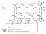
- FIG. 2A illustrates the configuration of the SSST transmitter.
- SSST transmitter is designed with parallel segments (viewed vertically) of paired, connected, transistors and resistors. Each segment consists of pull-up and pull-down elements that are switched by the input data to produce the output waveform.
- the pull-up elements comprise a P-type transistor 230 connected at its source to the high input rail (V HH ) 240 and at its drain to pull up resistor 237 .
- Pull-down elements include N-type transistor 235 , which is connected to low input rail (V LL ) 245 at its source and to pull up resistor 239 at its drain. Pull up resistor 237 and pull down resistor 239 are connected (in series) at a common node, which node is connected through each segment and produces the output signal 250 .
- SSST transmitter 200 is divided into a number of independently controllable segments. Only four segments are provided within the illustration; However, as suggested by the dashed lines, the number of segments actually utilized is a design parameter tied to the granularity of control desired for the SSST transmitter 200 . Thus, for example, the SSST transmitter 200 may comprise 16, 20, 32, 64, or any other number of segments.
- the segments each have particular output impedance such that their parallel combination is equal to the desired channel termination impedance.
- the impedance of each segment may be a combination of the resistor impedances and the transistor impedances; However, it is conceivable that the transistors utilized be sufficiently small to produce a desired impedance without requiring pull up and/or pull down resistive elements. Similarly, the transistors may be sufficiently large that they produce negligible impedances, whereby each segment's impedance value is respectively equal to either the pull up or pull down resistor, since only one transistor (switch) is on at a time.
- the transistors utilized are MOS transistors (i.e., P-MOS and N-MOS transistors). While described as MOS transistors, it is understood that the invention maybe practiced with different types of transistors and is thus not limited to those disclosed herein. For example, the transistors may be other types of FETs, bipolar transistors, and the like.
- MOS transistors i.e., P-MOS and N-MOS transistors. While described as MOS transistors, it is understood that the invention maybe practiced with different types of transistors and is thus not limited to those disclosed herein.
- the transistors may be other types of FETs, bipolar transistors, and the like.
- FIG. 2B the provided illustration is of only one half (a top or bottom half) of a complete differential transmitter, as illustrated by FIG. 2B , with both halves 200 A, 200 B being identical.
- the actual transmitter output( 275 ) is thus a combination (using adder 270 , for example) of the outputs at both halves 200 A, 200
- FIGS. 3 and 4 similarly represent only a single half of the complete differential transmitter.
- each segment is the gate input applied to the PMOS transistor 237 and NMOS transistor 235 .
- each segment's input is a buffered input received from a respective buffer 220 (or inverting buffer) that actually receives both the data input 205 and a complement of the data input, i.e., inverted data input 207 from the input source (not shown).
- Individualized amplitude control inputs 210 are fed to the buffers 220 and serve as select inputs to enable the buffer to pass either the normal data input 205 or the inverted data input 207 to the particular segment. For example, if the amplitude control input 210 is a 1, then the inverted data is sent to the segment, while if the amplitude control is a 0, then the normal data input is sent to the segment. In the illustrative embodiment, if amplitude control input 210 is a 0, the buffer 220 passes normal data input 205 to the segment. Alternatively, if amplitude control input 210 is a 1, buffer 220 passes inverted data input 207 to the segment.
- the data input passed is either a 1 or 0, which respectively turns on either the P-type transistor ( 230 ) or the N-type transistor ( 235 ). That is, when the data selected to pass through buffer is a 0, the 0 input data causes the upper branch of the segment to be pulled-up by turning on the P-type transistor (while shutting off the N-type transistor). Conversely, when the data selected to pass through buffer is a 1, the 1 input data causes the lower branch of the segment to be pulled-down by turning on the N-type transistor (while shutting off the P-type transistor). While the pull-up and pull-down operations are occurring, the resistance across the segment remains the same.
- the SSST transmitter enables selectable reduction of output amplitude without reducing or affecting the termination impedance. This method produces amplitudes which are defined fractions of the maximum amplitude while allowing the supply voltage to remain large enough for acceptable circuit performance.
- the percentage reduction of the output voltage may be calculated utilizing the total number of segments and the number of segments being driven with an inverted input signal.
- the calculation involves a subtraction of two times the inverted segments since the inverted segments cancel the voltage gain for an equal number of non-inverted segments.
- the output signal will be a negative value, indicating a reverse in polarity of the output signal.
- the ideal differential peak-to-peak output amplitude is equal to V HH ⁇ V LL .
- amplitude control is provided by statically setting a set (one or more) of the segments to received inverted input from the remaining segments.
- the segments are statically set.
- Similar amplitude reduction and constant impedance is provided as with the dynamic method of setting segments described above (illustrated by amplitude control inputs of FIG. 2A ).
- This embodiment provides a set output voltage relative to the input voltage.
- the segmentation method of amplitude control is combined with the voltage regulator method (described in the related section above) to provide very flexible and accurate transmitter amplitude control.
- the constant regulator provides amplitude accuracy and a supply level that allows good circuit performance, while the segmentation allows the amplitude to be adjustable while maintaining the desired output impedance.
- Pre-emphasis refers to the process whereby high frequency components are emphasized relative to low frequency components to improve the overall signal-to-noise (SN) ratio during transmission across the transmission channel.
- SN signal-to-noise
- pre-emphasis attempts to mitigate (or minimize the adverse effects of) the bandwidth limitations of the channel and the resulting inter-symbol interference (ISI).
- ISI inter-symbol interference
- serial link transmitters typically provide an adjustable output signal pre-emphasis capability by a structure analogous to a finite-impulse-response (FIR) digital filter, in which delayed versions of the output signal are subtracted from the main signal to create a high-pass characteristic that partially cancels the low-pass characteristic of the channel.
- FIR finite-impulse-response
- SSST transmitter 200 of FIG. 2A further adapted/enhanced to provide pre-emphasis control, according to one embodiment.
- SSST transmitter 200 comprises a different input to enable pre-emphasis control.
- SSST transmitter of FIG. 3 includes delay element 360 followed by inverter 365 that delays a copy of the input signal routed along the second input path to the buffers 220 and then inverts the delayed copy of the input.
- the delay element 360 delays the received input signal by one bit time (i.e., the time for one bit of the input signal to pass through the input). From the perspective of the buffer 220 , the inputs received at time T 1 are the normal data input 205 and the inverted data input from time T 0 . That is, assuming the data input at the primary input path (normal data input) to buffer 220 is 10101100, the input seen at the secondary input path is ⁇ 0101001.
- a plurality of delay elements may be provided to enable multiple delayed versions of the data stream. For example, a delay by 1, 2, 3, or more bit time may be provided.
- the SSST transmitter is designed to be compatible with this general pre-emphasis approach, simply by supplying the appropriately delayed data to a group of segments.
- adjustable pre-emphasis control may be implemented within the specific implementation of a self-series terminated transmitter, namely the SSST transmitter 300 .
- the segments have output impedances such that their parallel combination is equal to the desired channel termination impedance.
- each segment consists of pull-up and pull-down elements that are selectively switched by the input data to produce the output waveform.
- a particular level of pre-emphasis is created by driving a selected subset of the segments with delayed, inverted data (from buffer). Assuming that a single segment is biased to receive the delayed, inverted input data (i.e., select input to buffer always turned on “1”), then for the first data bit after a transition, all the segments pull in the same direction and the transmitter produces a full amplitude output. This enables the transmitter to produce the full amplitude instantaneously during each transition. For a switching run length greater than one bit (i.e., consecutive 0s or 1s), the delayed segments pull in the opposite direction, and the resulting impedance division reduces the output to a defined fraction of the full amplitude. This occurrence thus in effect “de-emphasizes” the lower frequencies.
- the overall effect of the extended input to the SSST transmitter 300 is to delay, invert, and subtract an input from the overall output being produced through the SSST transmitter 300 .
- segmentation schemes for amplitude and pre-emphasis control are completely compatible and may thus be provided within the same SSST transmitter. With this dual function SSST transmitter, some of the segments would be dedicated to pre-emphasis control while all others would be dedicated to amplitude control.
- serial link transmitters are designed with the capability to adjust their output signal slew rate.
- Slew rate refers to the maximum rate of change of the transmitter's output voltage. That is, the slew rate provides a measure of how fast the output moves, measured in volts per second. An incorrect slew rate may lead to cross talk interference with other channels.
- FIG. 4 provides an enhancement to the SSST transmitter 400 that illustrates how segmentation of the self-series terminated transmitter circuit provides a means to control the output slew rate.
- Each output segment is driven by a separate buffer (also referred to as a pre-buffer) 220 which may be made to take on a high output impedance state.
- the output of each pre-buffer 220 is permanently connected to the output of a previous segment's pre-buffer via a slew-control resistor 432 . This connection to the slew-control resistor is in addition to the connection to the gates of the P-type and N-type transistors of the segment.
- one end of a slew-control resistor 432 is coupled to the output of a first pre-buffer 220 ′ and the other end of the slew-control resistor 432 is also coupled to a next (in sequence) pre-buffer output ( 220 ′′), as shown by the figure.
- each subsequent pre-buffer 220 that has a horizontal resistor 432 connected to its output is turned off (placed in the off state) so that no input data signal is passed through that pre-buffer 220 .
- the determination of which sequence of pre-buffer outputs to cross-connect with slew-control resistors 432 and which pre-buffers 220 are subsequently turn off is a design determination. However, only pre-buffers whose outputs are the same (i.e., normal input data or inverted input data) are series connected in this manner. Two different sets of series connected pre-buffer outputs may be provided within the SSST transmitter 400 .
- a first pre-buffer 220 ′ in the series of connected pre-buffers operates as the driver of each of the connected segments. With the subsequent pre-buffers in the series shut off, the segments corresponding to these pre-buffers receive input from the first pre-buffer through the slew-control resistor(s) 432 .
- the first pre-buffer 220 ′ services an increased load (slew-control resistors 432 and transistors of subsequent segments) and thus the speed of its output transition is slowed down. Additionally, the slew-control resistors 432 themselves create a delay, which causes the segments to switch at different times (in sequence).
- the output is also received at a slower rate compared to the earlier switched segments.
- the output signal is thus delayed and has to wait until the latter switched segments go to the same state as the earlier switched segments.
- the SSST transmitter's output slew rate may be reduced by placing a portion of the pre-buffers 220 within the entire group into their high impedance state and allowing the remaining pre-buffers 220 to drive all the output segments in the group.
- the output segments that are driven through the slew-control resistors 432 experience a small delay in receiving the signal at their input. These delays reduce the output slew rate when the outputs of the segments are summed at the final transmitter output.
- control signals received from the buffers 220 may be utilized to determine which pre-buffers should be placed in the off state.
- control signals received from the buffers 220 may be utilized to determine which pre-buffers should be placed in the off state.
- any segment (other then the first segment) among the multiple available segments may be wired to receive its input signal through the slew control resistors 432 and that the specific depiction and description provided herein are meant solely for illustrating the invention.
Landscapes
- Engineering & Computer Science (AREA)
- Power Engineering (AREA)
- Computer Networks & Wireless Communication (AREA)
- Signal Processing (AREA)
- Computer Hardware Design (AREA)
- Physics & Mathematics (AREA)
- Computing Systems (AREA)
- General Engineering & Computer Science (AREA)
- Mathematical Physics (AREA)
- Dc Digital Transmission (AREA)
- Logic Circuits (AREA)
Priority Applications (3)
| Application Number | Priority Date | Filing Date | Title |
|---|---|---|---|
| US11/263,138 US7307447B2 (en) | 2005-10-27 | 2005-10-27 | Self series terminated serial link transmitter having segmentation for amplitude, pre-emphasis, and slew rate control and voltage regulation for amplitude accuracy and high voltage protection |
| JP2006284417A JP4267655B2 (ja) | 2005-10-27 | 2006-10-18 | 電子回路、該電子回路として構成された差分送信機、及び、自己直列終端送信機を形成する方法(振幅制御、プリ・エンファシス制御及びスルー・レート制御のためのセグメント化と振幅精度及び高電圧保護のための電圧調整とを有する自己直列終端シリアル・リンク送信機) |
| CNB2006101371216A CN100571226C (zh) | 2005-10-27 | 2006-10-20 | 自串联端接串行链路发射器及其制造方法 |
Applications Claiming Priority (1)
| Application Number | Priority Date | Filing Date | Title |
|---|---|---|---|
| US11/263,138 US7307447B2 (en) | 2005-10-27 | 2005-10-27 | Self series terminated serial link transmitter having segmentation for amplitude, pre-emphasis, and slew rate control and voltage regulation for amplitude accuracy and high voltage protection |
Publications (2)
| Publication Number | Publication Date |
|---|---|
| US20070103186A1 US20070103186A1 (en) | 2007-05-10 |
| US7307447B2 true US7307447B2 (en) | 2007-12-11 |
Family
ID=38003123
Family Applications (1)
| Application Number | Title | Priority Date | Filing Date |
|---|---|---|---|
| US11/263,138 Expired - Lifetime US7307447B2 (en) | 2005-10-27 | 2005-10-27 | Self series terminated serial link transmitter having segmentation for amplitude, pre-emphasis, and slew rate control and voltage regulation for amplitude accuracy and high voltage protection |
Country Status (3)
| Country | Link |
|---|---|
| US (1) | US7307447B2 (enExample) |
| JP (1) | JP4267655B2 (enExample) |
| CN (1) | CN100571226C (enExample) |
Cited By (15)
| Publication number | Priority date | Publication date | Assignee | Title |
|---|---|---|---|---|
| US20070124518A1 (en) * | 2005-07-28 | 2007-05-31 | Hideo Fujiwara | Transmitter driver circuit in high-speed serial communications system |
| US7511530B1 (en) | 2008-07-25 | 2009-03-31 | International Business Machines Corporation | Nodal charge compensation for SST driver having data mux in output stage |
| US20090102511A1 (en) * | 2007-10-18 | 2009-04-23 | Elpida Memory, Inc. | Semiconductor device and driver control method |
| US20110001463A1 (en) * | 2009-07-06 | 2011-01-06 | Young-Chan Jang | Transceiver for Controlling Swing Width of Output Voltage |
| US20120119792A1 (en) * | 2010-11-11 | 2012-05-17 | Advanced Micro Devices, Inc. | Adjustable finite impulse response transmitter |
| US20120147944A1 (en) * | 2009-09-14 | 2012-06-14 | Rambus Inc | High resolution output driver |
| US8410818B1 (en) * | 2012-02-14 | 2013-04-02 | Taiwan Semiconductor Manufacturing Co., Ltd. | High speed communication interface with an adaptive swing driver to reduce power consumption |
| US8618833B1 (en) | 2012-06-19 | 2013-12-31 | International Business Machines Corporation | Source series terminated driver circuit with programmable output resistance, amplitude reduction, and equalization |
| US20140159769A1 (en) * | 2012-12-12 | 2014-06-12 | Chan H. Hong | Programmable equalization with compensated impedance |
| US8786323B2 (en) | 2012-04-03 | 2014-07-22 | Samsung Electronics Co., Ltd. | Driver with resistance calibration capability |
| WO2014120450A1 (en) * | 2013-01-31 | 2014-08-07 | International Business Machines Corporation | Esd protection device for sst transmitter |
| KR101427517B1 (ko) | 2013-03-18 | 2014-08-07 | 고려대학교 산학협력단 | 데이터 송신 방법 및 장치 |
| US8878568B1 (en) * | 2011-09-12 | 2014-11-04 | Semtech Corporation | High-speed SSR transmit driver |
| US8989254B2 (en) | 2012-12-21 | 2015-03-24 | Avago Technologies General Ip (Singapore) Pte. Ltd. | Single serdes transmitter driver design for both ethernet and peripheral component interconnect express applications |
| US10192590B1 (en) * | 2017-10-19 | 2019-01-29 | Globalfoundries Inc. | Differential voltage generator |
Families Citing this family (16)
| Publication number | Priority date | Publication date | Assignee | Title |
|---|---|---|---|---|
| DE102005024643B4 (de) * | 2005-05-25 | 2013-09-05 | Krohne S.A. | Abtastschaltung |
| US7995660B2 (en) * | 2007-10-31 | 2011-08-09 | International Business Machines Corporation | Receiver termination circuit for a high speed direct current (DC) serial link |
| US7936180B2 (en) * | 2008-02-01 | 2011-05-03 | Mediatek Inc. | Serial link transmitter |
| JP5540479B2 (ja) * | 2008-08-26 | 2014-07-02 | 株式会社リコー | ドライバ回路 |
| US8395411B2 (en) * | 2010-10-08 | 2013-03-12 | Qualcomm Incorporated | Constant impedance line driver with digitally controlled edge rate |
| US8432184B2 (en) * | 2011-04-22 | 2013-04-30 | Mark Lasky | Termination device and system and method for termination for an alarm system peripheral device |
| US8760188B2 (en) * | 2011-06-30 | 2014-06-24 | Silicon Image, Inc. | Configurable multi-dimensional driver and receiver |
| JP5906960B2 (ja) | 2012-06-26 | 2016-04-20 | 富士通株式会社 | 半導体集積回路、信号伝送回路、信号伝送システム及び信号伝送方法 |
| US9419736B2 (en) * | 2013-03-15 | 2016-08-16 | Gigoptix-Terasquare Korea Co., Ltd. | Low-power CML-less transmitter architecture |
| US8912819B2 (en) * | 2013-03-18 | 2014-12-16 | Mediatek Inc. | Termination circuits capable of receiving data signals in different formats for performing impedance matching |
| US9337807B2 (en) * | 2014-09-30 | 2016-05-10 | Qualcomm Incorporated | Output driver circuit with auto-equalization based on drive strength calibration |
| WO2017173118A1 (en) * | 2016-03-30 | 2017-10-05 | Jariet Technologies, Inc. | Hybrid digital-to-analog conversion systems |
| US10583461B2 (en) | 2017-07-06 | 2020-03-10 | Texas Instruments Incorporated | Configurable pulser circuit operable across a range of supply voltages |
| US10892759B1 (en) * | 2020-02-19 | 2021-01-12 | Amazing Microelectronic Corp. | Bus driver module with controlled circuit and transition controlled circuit thereof |
| US11764733B2 (en) * | 2021-09-23 | 2023-09-19 | Qualcomm Incorporated | C-PHY receiver with self-regulated common mode servo loop |
| JP2024007690A (ja) | 2022-07-06 | 2024-01-19 | 富士通株式会社 | 光送信機 |
Citations (15)
| Publication number | Priority date | Publication date | Assignee | Title |
|---|---|---|---|---|
| US5194761A (en) | 1989-06-26 | 1993-03-16 | Dallas Semiconductor Corp. | Waveshaping subsystem using converter and delay lines |
| US5739707A (en) * | 1995-09-06 | 1998-04-14 | Lucent Technologies Inc. | Wave shaping transmit circuit |
| US5986489A (en) | 1996-04-03 | 1999-11-16 | Cypress Semiconductor Corp. | Slew rate control circuit for an integrated circuit |
| US6114885A (en) | 1997-08-22 | 2000-09-05 | Samsung Electronics Co., Ltd. | Integrated driver circuits having independently programmable pull-up and pull-down circuits therein which match load impedance |
| US20010000949A1 (en) | 1997-06-27 | 2001-05-10 | Sang-Jae Rhee | Integrated circuit memory devices having programmable output driver circuits therein |
| US6256235B1 (en) | 2000-06-23 | 2001-07-03 | Micron Technology, Inc. | Adjustable driver pre-equalization for memory subsystems |
| US6268750B1 (en) | 2000-01-11 | 2001-07-31 | Agilent Technologies, Inc. | Flattened resistance response for an electrical output driver |
| US6281715B1 (en) | 1998-04-29 | 2001-08-28 | National Semiconductor Corporation | Low voltage differential signaling driver with pre-emphasis circuit |
| US6313682B1 (en) | 1999-12-08 | 2001-11-06 | Analog Devices, Inc. | Pulse generation circuit and method with transmission pre-emphasis |
| US6353346B1 (en) | 2000-10-06 | 2002-03-05 | National Semiconductor Corporation | Apparatus and method for a programmable adaptive output driver |
| US6704818B1 (en) | 2000-12-29 | 2004-03-09 | Intel Corporation | Voltage-mode driver with pre-emphasis, slew-rate control and source termination |
| US6707324B1 (en) * | 2002-11-20 | 2004-03-16 | Via Technologies, Inc. | Low ground bounce output driver |
| US20060126401A1 (en) * | 2004-12-10 | 2006-06-15 | Micron Technology, Inc. | Reducing DQ pin capacitance in a memory device |
| US20060140309A1 (en) * | 2004-12-28 | 2006-06-29 | Industrial Technology Research Institute | Clock and data recovery circuits |
| US7078943B2 (en) * | 2003-04-22 | 2006-07-18 | Broadcom Corporation | Series terminated CMOS output driver with impedance calibration |
-
2005
- 2005-10-27 US US11/263,138 patent/US7307447B2/en not_active Expired - Lifetime
-
2006
- 2006-10-18 JP JP2006284417A patent/JP4267655B2/ja not_active Expired - Fee Related
- 2006-10-20 CN CNB2006101371216A patent/CN100571226C/zh active Active
Patent Citations (15)
| Publication number | Priority date | Publication date | Assignee | Title |
|---|---|---|---|---|
| US5194761A (en) | 1989-06-26 | 1993-03-16 | Dallas Semiconductor Corp. | Waveshaping subsystem using converter and delay lines |
| US5739707A (en) * | 1995-09-06 | 1998-04-14 | Lucent Technologies Inc. | Wave shaping transmit circuit |
| US5986489A (en) | 1996-04-03 | 1999-11-16 | Cypress Semiconductor Corp. | Slew rate control circuit for an integrated circuit |
| US20010000949A1 (en) | 1997-06-27 | 2001-05-10 | Sang-Jae Rhee | Integrated circuit memory devices having programmable output driver circuits therein |
| US6114885A (en) | 1997-08-22 | 2000-09-05 | Samsung Electronics Co., Ltd. | Integrated driver circuits having independently programmable pull-up and pull-down circuits therein which match load impedance |
| US6281715B1 (en) | 1998-04-29 | 2001-08-28 | National Semiconductor Corporation | Low voltage differential signaling driver with pre-emphasis circuit |
| US6313682B1 (en) | 1999-12-08 | 2001-11-06 | Analog Devices, Inc. | Pulse generation circuit and method with transmission pre-emphasis |
| US6268750B1 (en) | 2000-01-11 | 2001-07-31 | Agilent Technologies, Inc. | Flattened resistance response for an electrical output driver |
| US6256235B1 (en) | 2000-06-23 | 2001-07-03 | Micron Technology, Inc. | Adjustable driver pre-equalization for memory subsystems |
| US6353346B1 (en) | 2000-10-06 | 2002-03-05 | National Semiconductor Corporation | Apparatus and method for a programmable adaptive output driver |
| US6704818B1 (en) | 2000-12-29 | 2004-03-09 | Intel Corporation | Voltage-mode driver with pre-emphasis, slew-rate control and source termination |
| US6707324B1 (en) * | 2002-11-20 | 2004-03-16 | Via Technologies, Inc. | Low ground bounce output driver |
| US7078943B2 (en) * | 2003-04-22 | 2006-07-18 | Broadcom Corporation | Series terminated CMOS output driver with impedance calibration |
| US20060126401A1 (en) * | 2004-12-10 | 2006-06-15 | Micron Technology, Inc. | Reducing DQ pin capacitance in a memory device |
| US20060140309A1 (en) * | 2004-12-28 | 2006-06-29 | Industrial Technology Research Institute | Clock and data recovery circuits |
Non-Patent Citations (1)
| Title |
|---|
| Load Programmable Off-Chip Driver, IBM Technical Disclosure Bulletin, Jul. 1987, vol. 30 No. 2, pp. 950-951. |
Cited By (23)
| Publication number | Priority date | Publication date | Assignee | Title |
|---|---|---|---|---|
| US20070124518A1 (en) * | 2005-07-28 | 2007-05-31 | Hideo Fujiwara | Transmitter driver circuit in high-speed serial communications system |
| US7795919B2 (en) * | 2005-07-28 | 2010-09-14 | Ricoh Company, Ltd. | Transmitter driver circuit in high-speed serial communications system |
| US20090102511A1 (en) * | 2007-10-18 | 2009-04-23 | Elpida Memory, Inc. | Semiconductor device and driver control method |
| US7768312B2 (en) * | 2007-10-18 | 2010-08-03 | Elpida Memory, Inc. | Semiconductor device and driver control method |
| US7511530B1 (en) | 2008-07-25 | 2009-03-31 | International Business Machines Corporation | Nodal charge compensation for SST driver having data mux in output stage |
| US20110001463A1 (en) * | 2009-07-06 | 2011-01-06 | Young-Chan Jang | Transceiver for Controlling Swing Width of Output Voltage |
| US8143917B2 (en) * | 2009-07-06 | 2012-03-27 | Samsung Electronics Co., Ltd. | Transceiver for controlling swing width of output voltage |
| US8531206B2 (en) * | 2009-09-14 | 2013-09-10 | Rambus Inc. | High resolution output driver |
| US20120147944A1 (en) * | 2009-09-14 | 2012-06-14 | Rambus Inc | High resolution output driver |
| US8451031B2 (en) * | 2010-11-11 | 2013-05-28 | Advanced Micro Devices, Inc. | Adjustable finite impulse response transmitter |
| US20120119792A1 (en) * | 2010-11-11 | 2012-05-17 | Advanced Micro Devices, Inc. | Adjustable finite impulse response transmitter |
| US8878568B1 (en) * | 2011-09-12 | 2014-11-04 | Semtech Corporation | High-speed SSR transmit driver |
| US8410818B1 (en) * | 2012-02-14 | 2013-04-02 | Taiwan Semiconductor Manufacturing Co., Ltd. | High speed communication interface with an adaptive swing driver to reduce power consumption |
| US9099990B2 (en) | 2012-02-14 | 2015-08-04 | Taiwan Semiconductor Manufacturing Co., Ltd. | High speed communication interface with an adaptive swing driver to reduce power consumption |
| US8786323B2 (en) | 2012-04-03 | 2014-07-22 | Samsung Electronics Co., Ltd. | Driver with resistance calibration capability |
| US8618833B1 (en) | 2012-06-19 | 2013-12-31 | International Business Machines Corporation | Source series terminated driver circuit with programmable output resistance, amplitude reduction, and equalization |
| US20140159769A1 (en) * | 2012-12-12 | 2014-06-12 | Chan H. Hong | Programmable equalization with compensated impedance |
| US9048824B2 (en) * | 2012-12-12 | 2015-06-02 | Intel Corporation | Programmable equalization with compensated impedance |
| US8989254B2 (en) | 2012-12-21 | 2015-03-24 | Avago Technologies General Ip (Singapore) Pte. Ltd. | Single serdes transmitter driver design for both ethernet and peripheral component interconnect express applications |
| US8929040B2 (en) | 2013-01-31 | 2015-01-06 | International Business Machines Corporation | ESD protection device for SST transmitter |
| WO2014120450A1 (en) * | 2013-01-31 | 2014-08-07 | International Business Machines Corporation | Esd protection device for sst transmitter |
| KR101427517B1 (ko) | 2013-03-18 | 2014-08-07 | 고려대학교 산학협력단 | 데이터 송신 방법 및 장치 |
| US10192590B1 (en) * | 2017-10-19 | 2019-01-29 | Globalfoundries Inc. | Differential voltage generator |
Also Published As
| Publication number | Publication date |
|---|---|
| CN1956427A (zh) | 2007-05-02 |
| US20070103186A1 (en) | 2007-05-10 |
| JP2007124644A (ja) | 2007-05-17 |
| JP4267655B2 (ja) | 2009-05-27 |
| CN100571226C (zh) | 2009-12-16 |
Similar Documents
| Publication | Publication Date | Title |
|---|---|---|
| US7307447B2 (en) | Self series terminated serial link transmitter having segmentation for amplitude, pre-emphasis, and slew rate control and voltage regulation for amplitude accuracy and high voltage protection | |
| KR100433019B1 (ko) | 출력 버퍼 회로 | |
| US8228096B2 (en) | Circuit and method for current-mode output driver with pre-emphasis | |
| US9071243B2 (en) | Single ended configurable multi-mode driver | |
| US7164299B2 (en) | Output buffer circuit having pre-emphasis function | |
| US8258813B2 (en) | Circuit and method for driving at least one differential line | |
| EP1434347A1 (en) | Low voltage differential signaling (LVDS) driver with pre-emphasis | |
| US20090190648A1 (en) | Differential transmitter | |
| US7795919B2 (en) | Transmitter driver circuit in high-speed serial communications system | |
| US20090033365A1 (en) | Transmitting apparatus | |
| EP3539216B1 (en) | Apparatus and method for transmitting data signal based on different supply voltages | |
| US9419616B2 (en) | LVDS driver | |
| CN100566169C (zh) | 差动渥尔曼放大器电流型驱动器 | |
| US20120032656A1 (en) | Voltage regulator for impedance matching and pre-emphasis, method of regulating voltage for impedance matching and pre-emphasis, voltage mode driver including the voltage regulator, and voltage-mode driver using the method | |
| US7920014B2 (en) | Semiconductor integrated circuit device | |
| JP2012156763A (ja) | 送信回路 | |
| JP2003204291A (ja) | 通信システム | |
| US20130241602A1 (en) | Transmission circuit | |
| US11019392B2 (en) | Methods and apparatus for an output buffer | |
| US7348810B1 (en) | Push pull high-swing capable differential signaling circuits | |
| KR102646553B1 (ko) | 전압조정기 기반의 송신 이퀄라이제이션 장치 | |
| US6392443B1 (en) | Power/area efficient method for high-frequency pre-emphasis for chip to chip signaling | |
| CN120216429B (zh) | 一种时间和电流双向调节的预加重电路 | |
| JP2008147940A (ja) | 半導体集積回路 | |
| US10804924B2 (en) | Systems for reducing pattern-dependent inter-symbol interference and related methods |
Legal Events
| Date | Code | Title | Description |
|---|---|---|---|
| AS | Assignment |
Owner name: INTERNATIONAL BUSINESS MACHINES CORPORATION, NEW Y Free format text: ASSIGNMENT OF ASSIGNORS INTEREST;ASSIGNORS:CLEMENTS, STEVEN M.;CORNWELL, WILLIAM P.;COX, CARRIE E.;AND OTHERS;REEL/FRAME:017197/0474 Effective date: 20051027 |
|
| FEPP | Fee payment procedure |
Free format text: PAYOR NUMBER ASSIGNED (ORIGINAL EVENT CODE: ASPN); ENTITY STATUS OF PATENT OWNER: LARGE ENTITY |
|
| STCF | Information on status: patent grant |
Free format text: PATENTED CASE |
|
| FPAY | Fee payment |
Year of fee payment: 4 |
|
| FPAY | Fee payment |
Year of fee payment: 8 |
|
| SULP | Surcharge for late payment |
Year of fee payment: 7 |
|
| AS | Assignment |
Owner name: GLOBALFOUNDRIES U.S. 2 LLC, NEW YORK Free format text: ASSIGNMENT OF ASSIGNORS INTEREST;ASSIGNOR:INTERNATIONAL BUSINESS MACHINES CORPORATION;REEL/FRAME:036550/0001 Effective date: 20150629 |
|
| AS | Assignment |
Owner name: GLOBALFOUNDRIES INC., CAYMAN ISLANDS Free format text: ASSIGNMENT OF ASSIGNORS INTEREST;ASSIGNORS:GLOBALFOUNDRIES U.S. 2 LLC;GLOBALFOUNDRIES U.S. INC.;REEL/FRAME:036779/0001 Effective date: 20150910 |
|
| AS | Assignment |
Owner name: WILMINGTON TRUST, NATIONAL ASSOCIATION, DELAWARE Free format text: SECURITY AGREEMENT;ASSIGNOR:GLOBALFOUNDRIES INC.;REEL/FRAME:049490/0001 Effective date: 20181127 |
|
| MAFP | Maintenance fee payment |
Free format text: PAYMENT OF MAINTENANCE FEE, 12TH YEAR, LARGE ENTITY (ORIGINAL EVENT CODE: M1553); ENTITY STATUS OF PATENT OWNER: LARGE ENTITY Year of fee payment: 12 |
|
| AS | Assignment |
Owner name: GLOBALFOUNDRIES U.S. INC., CALIFORNIA Free format text: ASSIGNMENT OF ASSIGNORS INTEREST;ASSIGNOR:GLOBALFOUNDRIES INC.;REEL/FRAME:050122/0001 Effective date: 20190821 |
|
| AS | Assignment |
Owner name: MARVELL INTERNATIONAL LTD., BERMUDA Free format text: ASSIGNMENT OF ASSIGNORS INTEREST;ASSIGNOR:GLOBALFOUNDRIES U.S. INC.;REEL/FRAME:051070/0625 Effective date: 20191105 |
|
| AS | Assignment |
Owner name: CAVIUM INTERNATIONAL, CAYMAN ISLANDS Free format text: ASSIGNMENT OF ASSIGNORS INTEREST;ASSIGNOR:MARVELL INTERNATIONAL LTD.;REEL/FRAME:052918/0001 Effective date: 20191231 |
|
| AS | Assignment |
Owner name: MARVELL ASIA PTE, LTD., SINGAPORE Free format text: ASSIGNMENT OF ASSIGNORS INTEREST;ASSIGNOR:CAVIUM INTERNATIONAL;REEL/FRAME:053475/0001 Effective date: 20191231 |
|
| AS | Assignment |
Owner name: GLOBALFOUNDRIES INC., CAYMAN ISLANDS Free format text: RELEASE BY SECURED PARTY;ASSIGNOR:WILMINGTON TRUST, NATIONAL ASSOCIATION;REEL/FRAME:054636/0001 Effective date: 20201117 |