US7298485B2 - Method of and a device for measuring optical absorption characteristics of a sample - Google Patents
Method of and a device for measuring optical absorption characteristics of a sample Download PDFInfo
- Publication number
- US7298485B2 US7298485B2 US11/200,086 US20008605A US7298485B2 US 7298485 B2 US7298485 B2 US 7298485B2 US 20008605 A US20008605 A US 20008605A US 7298485 B2 US7298485 B2 US 7298485B2
- Authority
- US
- United States
- Prior art keywords
- light
- guide
- optical
- sample
- optical wave
- Prior art date
- Legal status (The legal status is an assumption and is not a legal conclusion. Google has not performed a legal analysis and makes no representation as to the accuracy of the status listed.)
- Expired - Fee Related, expires
Links
Images


Classifications
-
- G—PHYSICS
- G01—MEASURING; TESTING
- G01N—INVESTIGATING OR ANALYSING MATERIALS BY DETERMINING THEIR CHEMICAL OR PHYSICAL PROPERTIES
- G01N21/00—Investigating or analysing materials by the use of optical means, i.e. using sub-millimetre waves, infrared, visible or ultraviolet light
- G01N21/17—Systems in which incident light is modified in accordance with the properties of the material investigated
- G01N21/55—Specular reflectivity
- G01N21/552—Attenuated total reflection
-
- G—PHYSICS
- G01—MEASURING; TESTING
- G01N—INVESTIGATING OR ANALYSING MATERIALS BY DETERMINING THEIR CHEMICAL OR PHYSICAL PROPERTIES
- G01N21/00—Investigating or analysing materials by the use of optical means, i.e. using sub-millimetre waves, infrared, visible or ultraviolet light
- G01N21/17—Systems in which incident light is modified in accordance with the properties of the material investigated
- G01N21/25—Colour; Spectral properties, i.e. comparison of effect of material on the light at two or more different wavelengths or wavelength bands
- G01N21/31—Investigating relative effect of material at wavelengths characteristic of specific elements or molecules, e.g. atomic absorption spectrometry
- G01N21/314—Investigating relative effect of material at wavelengths characteristic of specific elements or molecules, e.g. atomic absorption spectrometry with comparison of measurements at specific and non-specific wavelengths
-
- G—PHYSICS
- G01—MEASURING; TESTING
- G01N—INVESTIGATING OR ANALYSING MATERIALS BY DETERMINING THEIR CHEMICAL OR PHYSICAL PROPERTIES
- G01N2201/00—Features of devices classified in G01N21/00
- G01N2201/06—Illumination; Optics
- G01N2201/066—Modifiable path; multiple paths in one sample
-
- G—PHYSICS
- G01—MEASURING; TESTING
- G01N—INVESTIGATING OR ANALYSING MATERIALS BY DETERMINING THEIR CHEMICAL OR PHYSICAL PROPERTIES
- G01N2201/00—Features of devices classified in G01N21/00
- G01N2201/08—Optical fibres; light guides
Definitions
- the present invention relates to a method of measuring optical absorption characteristics of a sample having a quantity available for measurement that is extremely small by using an optical wave-guide.
- the present invention also relates to a device for measuring the optical absorption characteristics of the sample having very small quantity by using the optical wave-guide.
- a method of measuring an optical absorption characteristics of a sample comprises conducting a light to the sample so that the light is reflected on the sample by a total reflection, receiving the light that was reflected on the sample, and detecting the optical absorption characteristic of the sample on the basis of the received light in order to specify at least any one of a condition of a target substance in the sample, a kind of a target substance in the sample, a concentration of the target substance in the sample, and an amount of a target substance in the sample on the basis of the optical absorption characteristics of the sample.
- an optical wave-guide is used for reflecting the light reflected on the sample by the total reflection.
- the conventional optical wave-guide includes a trapezoid body or a rectangular parallelepiped body, so that the light is reflected by the total reflection several times in the optical wave-guide.
- the optical wave-guide has a pair of a light input surface 31 and a light output surface 32 that are opposite to each other, and a pair of an upper reflecting surface 33 and a bottom reflecting surface 34 that are opposite to each other.
- the sample 35 to be measured is disposed on the bottom reflecting surface 34 .
- a laser light or a white light from a light source not shown in the drawing is entered into the optical wave-guide through the input surface 31 , and the light continuously is reflected by the total reflection on the upper reflecting surface 33 and the bottom reflecting surface 34 .
- the light is reflected by the total reflection on the sample disposed on the bottom reflecting surface 34 several times so that the optical absorptions are produced through every total reflection.
- the optical absorption characteristics depend on the kind of the target substance in the sample.
- the condition of the target substance, the kind of the target substance, the concentration of the target substance and the amount of the target substance in the sample by detecting the optical absorption characteristics of the sample from the light that was reflected on the sample by the total reflection in the optical wave-guide and then exited from the optical wave-guide (Referring the Japanese patent No. 2807777).
- the optical absorption characteristics may be any one of an amount of the optical absorption, an optical absorption intensity, and an optical absorption spectrum.
- the measurement sensitivity of the above mentioned measuring method depends on the number of the reflecting times. More specifically, if the number of the reflecting times increases, the measurement sensitivity also increases. Conversely, if the number of the reflecting times decreases, the measurement sensitivity also decreases. Therefore, in order to increase the measurement sensitivity it is necessary to lengthen the optical wave-guide, or to thin the optical wave-guide, so that the number of the reflecting times is increased.
- the optical wave-guide is lengthened, the number of reflecting times increases as shown in FIG. 12( b ). However the area of the reflecting surface also enlarges, so that the amount of the sample to be required for measurement increases. Because it is difficult to extract the any kind of the samples that include a specimen that only trace amount thereof can be prepared or available, there is a serious problem that it becomes difficult to measure such a specimen if the increased amount thereof is required for measurement.
- a method of measuring an optical absorption characteristics of a sample comprises conducting a light from a light source to a optical wave-guide that has light input surface(s) and light output surface(s) that are opposite to each other, and a reflecting surface on which a sample to be measured is disposed, through which the light passes and is reflected by a total reflection on the sample, transmitting the light exited from the optical wave-guide through the output surface thereof to the input surface of the optical wave-guide so that the light is again entered into the optical wave-guide at least one time, receiving the light re-exited from the optical wave-guide, and detecting the optical absorption characteristics of the sample on the basis of the light received.
- a device for measuring an optical absorption characteristic of a sample comprises a light source, a optical wave-guide having light input surface(s) and light output surface(s) that are opposite to each other, and a light reflecting surface on which a sample to be measured is disposed, through which the light passes and is reflected by a total reflection on the sample, one or more light transmitting means arranged between the light output surface of the optical wave-guide and the light input surface of the optical wave-guide so that the light is again entered into the optical wave-guide, and a processing device which receives the light re-exited from the optical wave-guide through the output surface and detects the optical absorption characteristics of the sample on the basis of the light received, whereby the light which passes through the optical wave-guide is conducted to the optical wave-guide again, the light is again entered the optical wave-guide, and the light is again reflected on the sample.
- FIG. 1 is a schematic side view showing the first embodiment of the device for measuring the optical absorption characteristic of the sample according to the present invention.
- FIG. 2 is a schematic top view showing the device for measuring the optical absorption characteristics of the sample in FIG. 1 .
- FIG. 3 is a schematic side view showing the second embodiment of the device for measuring the optical absorption characteristics of the sample according to the present invention.
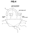
- FIG. 4 is a schematic side view showing the third embodiment of the device for measuring the optical absorption characteristics of the sample according to the present invention.
- FIG. 5 is a schematic side view showing the fourth embodiment of the device for measuring the optical absorption characteristics of the sample according to the present invention.
- FIG. 6 is a schematic perspective view showing the fifth embodiment of the device for measuring the optical absorption characteristics of the sample according to the present invention.
- FIG. 7 illustrates the function of the device for measuring the optical absorption characteristics of the sample shown in FIG. 6 .
- FIG. 8 illustrates the function of the device for measuring the optical absorption characteristics of the sample shown in FIG. 6 .
- FIG. 9 illustrates the function of the device for measuring the optical absorption characteristics of the sample shown in FIG. 6 .
- FIG. 10 is a schematic side view showing the sixth embodiment of the device for measuring the optical absorption characteristics of the sample according to the present invention.
- FIG. 11 is a schematic diagram showing the seventh embodiment of the device for measuring the optical absorption characteristics of the sample according to the present invention.
- FIGS. 12( a ) and 12 ( b ) show the conventional optical wave-guides.
- FIG. 1 is a schematic side view of the first embodiment of a device for measuring optical absorption characteristics of sample according to the present invention in order to explain the principle of a method of measuring optical absorption characteristics of a sample according to the present invention.
- FIG. 2 is a schematic top view of the device shown in FIG. 1 .
- the numeral number 1 indicates an optical wave-guide.
- the optical wave-guide 1 is a truncated six-sided pyramid shape.
- the truncated six-sided pyramid shape optical wave-guide 1 has six side surfaces 2 , i.e. three pairs of two side surfaces that are opposite to each other.
- first pair of two side surfaces 2 a and 2 b that are opposite to each other are used as a first input surface 2 a and a first output surface 2 b
- second pair of two side surfaces 2 c and 2 d that are opposite to each other are used as a second input surface 2 c and a second output surface 2 d .
- Said second output surface 2 d is a final output surface in this embodiment.
- the optical wave-guide 1 is made from transparent material having the refractive index by which the light may be guided by the total reflection through the optical wave-guide 1 , for example, silica glass or high refractive index glass.
- a sample 4 being measured is disposed on a bottom surface (a reflecting surface) 3 of the optical wave-guide.
- a light source 5 is arranged such that the laser light is entered into the optical wave-guide 1 through a predetermined first input point of the first input surface 2 a .
- the light thus is entered into the optical wave-guide.
- the light is reflected by the total reflection on a predetermined reflecting point of the sample disposed on the reflecting surface 3 .
- the laser light exits from the optical wave-guide 1 through a predetermined first output point of the first output surface 2 b .
- the first input point is symmetrically opposite to the first output point with respect to a central axis “a” that perpendicularly extends through the predetermined reflecting point of the reflecting surface 3 .
- An optical fiber 6 is arranged as a light transmitting means that is provided between the first output surface 2 b and the second input surface 2 c .
- the optical fiber 6 receives the laser light exited from the optical wave-guide 1 through the first output point of the first output surface 2 b , and transmits the light to a predetermined second input point of the second input surface 2 c.
- the light that is transmitted by the optical fiber 6 is again entered into the optical wave-guide through the second input point of the second input surface 2 c .
- the re-entered light is again reflected by the total reflection on said reflecting point of the sample disposed on the reflecting surface 3 .
- the light again exits from the optical wave-guide 1 through a second output point of the second output surface 2 d , which is symmetrically opposite to the second input point of the second input surface 2 c with respect to the central axis “a”.
- a processing device 7 is arranged such that it receives the laser light that was reflected two times by the total reflection on the sample in the optical wave-guide and then exited from the optical wave-guide 1 through the final output point (in this embodiment, the final output point is the second output point of the second output surface 2 d ).
- the processing device detects the optical absorption characteristics of the sample on the basis of the light, in order to specify the condition of the target substance, the kind of the target substance, the concentration of the target substance and the amount of the target substance in the sample.
- the optical absorption characteristics may be any one of an amount of the optical absorption, an optical absorption intensity, and an optical absorption spectrum.
- the optical absorption characteristics may be any one of an amount of the optical absorption, an optical absorption spectrum, and an optical absorption spectrum.
- the light from the light source is reflected two times by the total reflection at the same reflecting point of the sample so that the measuring sensitivity is higher than that obtained in the conventional method using the same optical wave-guide as that of the above embodiment in which the light is reflected only one time by the total reflection at the one reflecting point of the sample.
- the light is directly entered into the optical wave-guide from 1 the light source 5 , the light exited from the optical wave-guide 1 is directly received by the optical fiber 6 , and the light is directly re-entered into the optical wave-guide 1 from the optical fiber 6 .
- said construction of the light source 5 , the optical wave-guide 1 and the optical fiber 6 are not restricted to the above embodiment.
- a collective lens may be provided between the optical wave-guide 1 and the optical fiber 6 , or an end face of the optical fiber 6 may be formed to a lens like shape.
- the device for measuring the optical absorption characteristics is constructed such that the light is reflected two times by the total reflection on the sample in the optical wave-guide 1 .
- the number of light reflecting times is not restricted to the above embodiment.
- an another optical fiber which may transmit the light exited from the optical wave-guide through the second output surface 2 d to a third input surface 2 e may be provided, so that the light is re-entered into the optical wave-guide two times and the light is reflected three time by the total reflection on the same reflecting point of the sample in the optical wave-guide 1 .
- the processing device 7 must be arranged such that it receives the laser light exited from the optical wave-guide 1 through a third output point of a third output surface 2 f , which is symmetrically opposite to the third input point of the third input surface 2 e with respect to the central axis “a”.
- the number of the light reflecting times may be arbitrarily increased with four times, five times, and more times by forming the optical wave-guide to a truncated eight-side pyramid shape or a truncated ten-side pyramid shape and increasing the number of pairs of two surfaces that are opposite to each other, which consists of the input surface and output surface of the optical wave-guide.
- the optical wave-guide may be formed to the hemisphere shape. In this case, the light input point and the light output point may be determined without the side surface.
- optical wave-guide of the truncated shape mentioned in the illustrated embodiment regardless of the truncated cone or pyramid shape, it is possible to use the optical wave-guide in a position reversed to that of the illustrated embodiment.
- FIG. 4 illustrates a case where the optical wave-guide of the truncated pyramid shape is used in a position reversed to that of the embodiment of FIG. 1 .
- the incident light is reflected on the inclined surface 1 a of the optical wave-guide and is conducted to the sample 4 .
- the light is reflected by the total reflection on the sample 4 and is reflected on the inclined surface 1 b .
- the reflected light exits from the optical wave-guide 1 .
- the inclined surfaces 1 a and 1 b are used only for the reflection of the light.
- the sample 4 may be disposed on the inclined surfaces 1 a and 1 b .
- These inclined surfaces 1 a and 1 b as well as the bottom surface 3 may be intended to make the total reflection of light.
- the optical wave-guide is not necessarily the truncated shape. Alternatively, it may be a cone or pyramid shape (See FIG. 5 ).
- input points and output points are positioned on the different surface, respectively.
- the positions of the input point and output point are not restricted to the above embodiment.
- a matrix assembly of a number of optical fibers may be arranged such that a number of input points through which the light is entered and re-entered into the optical wave-guide from each of the optical fiber of the matrix are arranged on the same input surface and a number of output point through which the light exits and re-exits from the optical wave-guide are arranged on the same output surface.
- FIGS. 6 to 9 show fifth embodiment of a device for measuring the optical absorption characteristics of the sample according to the present invention.
- the device for measuring the optical absorption characteristics has a matrix assembly that consists of four optical fibers.
- the matrix assembly is arranged between an input surface and an output surface of a prism 21 as an optical wave-guide, so that four input points are positioned on the same input surface of the prism 21 and four output points are positioned on the same output surface of the prism 21 .
- numeral numbers 20 a to 20 e indicate optical fibers
- numeral number 22 indicates a reflecting surface of the prism, on which a sample being measured is disposed.
- a light A from a light source is entered into the prism 21 through the optical fiber 20 a , and then the light A is reflected by the total reflection on the sample of the reflecting surface 22 . By way of the total reflection, the light A exits from the prism 21 and is received by the optical fiber 20 b.
- the optical fiber 20 b transmits the light to the input surface of the prism 21 .
- the light B from the optical fiber 20 b is re-entered into the prism 21 , and then the light B is re-reflected by the total reflection on the sample on the reflecting surface 22 .
- the light B re-exits from the prism 21 and is received by the optical fiber 20 c .
- the optical fiber 20 c transmits the light to the input surface of the prism 21 .
- the light C from the optical fiber 20 c is again entered into the prism 21 , and then the light C is again reflected by the total reflection on the sample on the reflecting surface 22 . After that, the light C re-exits from the prism 21 and is received by the optical fiber 20 d .
- the optical fiber 20 d transmits the light to the input surface of the prism 21 .
- the light D form the optical fiber 20 d is re-entered into the prism 21 , and then the light D is re-reflected by the total reflection on the sample on the reflecting surface 22 . After that, the light D re-exits from the prism 21 , and is received by the optical fiber 20 e .
- the optical fiber 20 e is connected to a processing device not shown in drawing.
- the matrix assembly consists of the four optical fibers.
- the number of the optical fibers of the matrix is not restricted to the above embodiment.
- the matrix assembly may be made from the one hundred optical fibers each of which has a diameter of 0.1 mm, so that the light may be reflected one hundred times on the sample within an area of 1 mm 2 .
- the optical wave-guide is truncated four-side pyramid, i.e. has two pairs of the input surface and output surface.
- one matrix assembly made from the one hundred optical fibers each of which has a diameters of 0.1 mm is arranged between the first input surface of the optical wave-guide and the first output surface of the optical wave-guide, and other matrix assembly made from the one hundred optical fibers each of which has a diameters of 0.1 mm between the second input surface of the optical wave-guide and the second output surface of the optical wave-guide.
- the light is perpendicularly entered with respect to the input surface and the light perpendicularly exits with respect to the output surface.
- the input angle and the output angle of the light is not restricted to the above embodiment, for example, as shown in FIG. 10 the light may be refracted by using the inclination of the input surface 2 a and output surface 2 b of the optical wave-guide 1 in order to direct the light to the sample 4 .
- the seventh embodiment of an device for measuring an optical absorption characteristics of a sample according to the present invention will be described with reference to the FIG. 11 .
- the device for measuring the optical absorption characteristics comprises housing 10 in which a light source 5 , an optical fiber 6 , and an optical receiving element 7 are provided.
- the device for measuring the optical absorption characteristics also comprises an optical wave-guide in which a sample to be measured is disposed.
- the optical fiber 6 transmits the light exited from the optical wave-guide to the optical wave-guide again, so that the light is re-entered into the optical wave-guide and the light is again reflected on the sample disposed on the optical wave-guide.
- the device for measuring the optical absorption characteristics also comprises a processing device 11 that detects the optical absorption characteristics of the sample disposed on the optical wave-guide on the basis of the light that was reflected on the sample several times in the optical wave-guide, exits from the optical wave-guide, and then is received by the optical receiving element 7 .
- the processing results of the processing device 11 are displayed on a display 12 .
- the light source 5 , the optical fiber 6 , the optical receiving element 7 , the processing device 11 , and the display 12 are provided in the housing 10 , so that it is possible to provide an all-in-one portable type device for measuring the optical absorption characteristics that is novelty.
- the size of the all-in-one type portable device for measuring the optical absorption characteristics depends on the size of the optical wave-guide.
- the above device for measuring the optical absorption characteristics has the optical fiber 6 by which the light is returned from the output surface to the input surface of the optical wave-guide, so that the light is re-entered into the optical wave-guide and is re-reflected on the sample in the optical wave-guide.
- the optical absorption measuring device may be portable.
- the light source 5 , the optical fiber 6 , the optical receiving element 7 , the processing device 11 , and the display 12 are provided in one housing, however the construction of the device for measuring the optical absorption characteristics of sample is not restricted to the above-mentioned embodiment.
- the result is displayed with the display.
- the construction of the device for measuring the optical absorption characteristics according to the present invention is not restricted the above-mentioned embodiment, for example, the result may be output by using the printer, the any type of a storage media, a lump, or a speaker.
- the optical fiber is provided in the housing in order to return the light from the output surface of the optical wave-guide to the input surface of the optical wave-guide, so that the light is re-entered into the optical wave-guide.
- the construction of the light transmitting means is not restricted to the embodiment in FIG. 11 .
- a matrix assembly of a number of the optical fibers may be provided in the housing in place of the optical fiber, so that a lot of reflection times may be obtained.
- the P-type light polarizer (longitudinal wave) or S-type light polarizer (transverse wave) may be provided between the optical fiber and the optical wave-guide, so that it is possible to detect the direction of the molecule in the sample arranged on the reflecting surface.
Landscapes
- Physics & Mathematics (AREA)
- Health & Medical Sciences (AREA)
- Life Sciences & Earth Sciences (AREA)
- Chemical & Material Sciences (AREA)
- Analytical Chemistry (AREA)
- Biochemistry (AREA)
- General Health & Medical Sciences (AREA)
- General Physics & Mathematics (AREA)
- Immunology (AREA)
- Pathology (AREA)
- Spectroscopy & Molecular Physics (AREA)
- Investigating Or Analysing Materials By Optical Means (AREA)
Applications Claiming Priority (2)
| Application Number | Priority Date | Filing Date | Title |
|---|---|---|---|
| JP2004-244032 | 2004-08-24 | ||
| JP2004244032A JP4516803B2 (ja) | 2004-08-24 | 2004-08-24 | 光吸収測定方法及び装置 |
Publications (2)
| Publication Number | Publication Date |
|---|---|
| US20060044560A1 US20060044560A1 (en) | 2006-03-02 |
| US7298485B2 true US7298485B2 (en) | 2007-11-20 |
Family
ID=35311790
Family Applications (1)
| Application Number | Title | Priority Date | Filing Date |
|---|---|---|---|
| US11/200,086 Expired - Fee Related US7298485B2 (en) | 2004-08-24 | 2005-08-10 | Method of and a device for measuring optical absorption characteristics of a sample |
Country Status (6)
| Country | Link |
|---|---|
| US (1) | US7298485B2 (ja) |
| EP (1) | EP1630545B1 (ja) |
| JP (1) | JP4516803B2 (ja) |
| KR (1) | KR20060050572A (ja) |
| CN (1) | CN1740776B (ja) |
| TW (1) | TWI283742B (ja) |
Families Citing this family (5)
| Publication number | Priority date | Publication date | Assignee | Title |
|---|---|---|---|---|
| US7233396B1 (en) | 2006-04-17 | 2007-06-19 | Alphasniffer Llc | Polarization based interferometric detector |
| CN102478505B (zh) * | 2010-11-30 | 2015-06-10 | 新奥科技发展有限公司 | 用于测定流体光学参数的装置 |
| CN103115879B (zh) * | 2013-01-18 | 2015-05-06 | 北京林业大学 | 一种利用吸收光谱测定植物活体叶片中叶绿素a、叶绿素b和类胡萝卜素含量的方法 |
| KR101948975B1 (ko) * | 2016-05-30 | 2019-02-15 | 한국기술교육대학교 산학협력단 | 측정 체적이 확장된 에어로졸의 광흡수계수 측정시스템 |
| KR101884091B1 (ko) * | 2016-11-30 | 2018-08-02 | 한국표준과학연구원 | 사다리꼴 입사구조 프리즘 입사형 실리콘 기반 액침 미세유로 측정장치 및 측정방법 |
Citations (6)
| Publication number | Priority date | Publication date | Assignee | Title |
|---|---|---|---|---|
| US3415602A (en) | 1966-01-14 | 1968-12-10 | Philips Corp | Internal reflection element for micro-sample analysis |
| JPH0712715A (ja) | 1993-06-29 | 1995-01-17 | Shimadzu Corp | 全反射吸収スペクトル測定装置 |
| JP2000111474A (ja) | 1998-10-07 | 2000-04-21 | Mitsubishi Electric Corp | 高感度atr分析法及びそれに用いる光学プリズム |
| US20020126290A1 (en) * | 2001-01-25 | 2002-09-12 | Fuji Photo Film Co., Ltd. | Sensor utilizing attenuated total reflection |
| EP1371966A1 (en) | 2002-06-14 | 2003-12-17 | Stiftung Für Diagnostische Forschung | A cuvette for a reader device for assaying substances using the evanescence field method |
| US20050007596A1 (en) * | 2003-07-11 | 2005-01-13 | Wilks Enterprise, Inc. | Apparatus and method for increasing the sensitivity of in-line infrared sensors |
Family Cites Families (7)
| Publication number | Priority date | Publication date | Assignee | Title |
|---|---|---|---|---|
| US3415603A (en) * | 1967-03-17 | 1968-12-10 | Floyd W. Blanchard | Self-pressurizing retractable ballpoint pen |
| JPH01245134A (ja) * | 1988-03-28 | 1989-09-29 | Yokogawa Electric Corp | シート状物体の特性測定装置 |
| JPH03273138A (ja) * | 1990-03-22 | 1991-12-04 | Nec Corp | 光学式液質測定装置 |
| JPH05249035A (ja) * | 1992-03-10 | 1993-09-28 | F M T:Kk | 塩分検知方法 |
| JP2807777B2 (ja) | 1994-09-09 | 1998-10-08 | 工業技術院長 | スラブ光導波路を利用した光吸収スペクトル測定装置 |
| JPH08201278A (ja) * | 1995-01-20 | 1996-08-09 | Shimadzu Corp | スペクトル測定装置 |
| US5818046A (en) * | 1996-08-30 | 1998-10-06 | Rizvi; Syed A. | Mid-infrared analysis system |
-
2004
- 2004-08-24 JP JP2004244032A patent/JP4516803B2/ja not_active Expired - Fee Related
-
2005
- 2005-08-10 US US11/200,086 patent/US7298485B2/en not_active Expired - Fee Related
- 2005-08-12 EP EP20050356136 patent/EP1630545B1/en not_active Expired - Fee Related
- 2005-08-16 TW TW94127798A patent/TWI283742B/zh not_active IP Right Cessation
- 2005-08-23 KR KR20050077380A patent/KR20060050572A/ko active Search and Examination
- 2005-08-24 CN CN2005100977525A patent/CN1740776B/zh not_active Expired - Fee Related
Patent Citations (6)
| Publication number | Priority date | Publication date | Assignee | Title |
|---|---|---|---|---|
| US3415602A (en) | 1966-01-14 | 1968-12-10 | Philips Corp | Internal reflection element for micro-sample analysis |
| JPH0712715A (ja) | 1993-06-29 | 1995-01-17 | Shimadzu Corp | 全反射吸収スペクトル測定装置 |
| JP2000111474A (ja) | 1998-10-07 | 2000-04-21 | Mitsubishi Electric Corp | 高感度atr分析法及びそれに用いる光学プリズム |
| US20020126290A1 (en) * | 2001-01-25 | 2002-09-12 | Fuji Photo Film Co., Ltd. | Sensor utilizing attenuated total reflection |
| EP1371966A1 (en) | 2002-06-14 | 2003-12-17 | Stiftung Für Diagnostische Forschung | A cuvette for a reader device for assaying substances using the evanescence field method |
| US20050007596A1 (en) * | 2003-07-11 | 2005-01-13 | Wilks Enterprise, Inc. | Apparatus and method for increasing the sensitivity of in-line infrared sensors |
Non-Patent Citations (1)
| Title |
|---|
| Villagran J C et al; "Simplified attenuated total reflection apparatus"; Review of Scientific Instruments< AIP; vol. 60; No. 6; Jun. 1, 1989; pp. 1201-1202, XP000035898. |
Also Published As
| Publication number | Publication date |
|---|---|
| EP1630545A1 (en) | 2006-03-01 |
| US20060044560A1 (en) | 2006-03-02 |
| CN1740776B (zh) | 2010-05-12 |
| CN1740776A (zh) | 2006-03-01 |
| KR20060050572A (ko) | 2006-05-19 |
| TW200615532A (en) | 2006-05-16 |
| JP4516803B2 (ja) | 2010-08-04 |
| TWI283742B (en) | 2007-07-11 |
| EP1630545B1 (en) | 2013-01-02 |
| JP2006064405A (ja) | 2006-03-09 |
Similar Documents
| Publication | Publication Date | Title |
|---|---|---|
| US5625459A (en) | Diffuse reflectance probe | |
| US7298485B2 (en) | Method of and a device for measuring optical absorption characteristics of a sample | |
| US20150247795A1 (en) | Spectrometer with a relay lightpipe | |
| US6507402B2 (en) | SPR sensor plate and immune reaction measuring instrument using the same | |
| US20050018194A1 (en) | Surface plasmon resonance sensor | |
| US7062125B2 (en) | Prismatic reflection optical waveguide device | |
| JP3881960B2 (ja) | 携帯自動屈折計 | |
| CN112424575B (zh) | 测光装置 | |
| US10145789B2 (en) | Immersion refractometer | |
| EP3290907A1 (en) | Device for measuring solution concentration | |
| US5742382A (en) | Refractometer | |
| US7860355B2 (en) | ATR-probe | |
| CN215727691U (zh) | 一种折光仪 | |
| US6846085B2 (en) | Mitigating the effects of miniaturizing integrating spheres for fiber optic measurement | |
| CN211122485U (zh) | 一种测量液体浓度的检测勺 | |
| CN211122529U (zh) | 用于液体折射率测量的工作面聚光的集成化的探头结构 | |
| CN110320179B (zh) | 一种工作面聚光的液体折射率测试探头及其光折射方法 | |
| CN108572160A (zh) | 一种折射率分布测量的折光计 | |
| CN110398476A (zh) | 用于液体折射率测量的笔式布局的光学系统及其测量方法 | |
| JP2003185568A (ja) | 全反射減衰を利用したセンサー | |
| US10782231B2 (en) | Optical immersion refractometer | |
| US11249018B2 (en) | Optical refractometer and real time monitoring analysis device having the same | |
| Trierweiler et al. | Easy integrable refractometer for liquids on extended surfaces | |
| GB2621771A (en) | Capillary electrophoresis device | |
| JP2003065946A (ja) | 全反射減衰を利用したセンサー |
Legal Events
| Date | Code | Title | Description |
|---|---|---|---|
| AS | Assignment |
Owner name: SYSTEM INSTRUMENTS CO., LTD., JAPAN Free format text: ASSIGNMENT OF ASSIGNORS INTEREST;ASSIGNOR:TAKAHASHI, HIROMI;REEL/FRAME:016838/0920 Effective date: 20050725 |
|
| FEPP | Fee payment procedure |
Free format text: PAYOR NUMBER ASSIGNED (ORIGINAL EVENT CODE: ASPN); ENTITY STATUS OF PATENT OWNER: SMALL ENTITY |
|
| FEPP | Fee payment procedure |
Free format text: PAT HOLDER CLAIMS SMALL ENTITY STATUS, ENTITY STATUS SET TO SMALL (ORIGINAL EVENT CODE: LTOS); ENTITY STATUS OF PATENT OWNER: SMALL ENTITY |
|
| REFU | Refund |
Free format text: REFUND - PAYMENT OF MAINTENANCE FEE, 4TH YEAR, LARGE ENTITY (ORIGINAL EVENT CODE: R1551); ENTITY STATUS OF PATENT OWNER: SMALL ENTITY |
|
| FPAY | Fee payment |
Year of fee payment: 4 |
|
| REMI | Maintenance fee reminder mailed | ||
| LAPS | Lapse for failure to pay maintenance fees | ||
| STCH | Information on status: patent discontinuation |
Free format text: PATENT EXPIRED DUE TO NONPAYMENT OF MAINTENANCE FEES UNDER 37 CFR 1.362 |
|
| FP | Lapsed due to failure to pay maintenance fee |
Effective date: 20151120 |