US7190822B2 - Method for customizing an integrated circuit element - Google Patents
Method for customizing an integrated circuit element Download PDFInfo
- Publication number
- US7190822B2 US7190822B2 US10/312,632 US31263203A US7190822B2 US 7190822 B2 US7190822 B2 US 7190822B2 US 31263203 A US31263203 A US 31263203A US 7190822 B2 US7190822 B2 US 7190822B2
- Authority
- US
- United States
- Prior art keywords
- vectors
- vector
- circuit
- composite
- operators
- Prior art date
- Legal status (The legal status is an assumption and is not a legal conclusion. Google has not performed a legal analysis and makes no representation as to the accuracy of the status listed.)
- Expired - Fee Related, expires
Links
Images


Classifications
-
- G—PHYSICS
- G01—MEASURING; TESTING
- G01R—MEASURING ELECTRIC VARIABLES; MEASURING MAGNETIC VARIABLES
- G01R31/00—Arrangements for testing electric properties; Arrangements for locating electric faults; Arrangements for electrical testing characterised by what is being tested not provided for elsewhere
- G01R31/28—Testing of electronic circuits, e.g. by signal tracer
- G01R31/2832—Specific tests of electronic circuits not provided for elsewhere
- G01R31/2836—Fault-finding or characterising
- G01R31/2846—Fault-finding or characterising using hard- or software simulation or using knowledge-based systems, e.g. expert systems, artificial intelligence or interactive algorithms
-
- G—PHYSICS
- G01—MEASURING; TESTING
- G01R—MEASURING ELECTRIC VARIABLES; MEASURING MAGNETIC VARIABLES
- G01R31/00—Arrangements for testing electric properties; Arrangements for locating electric faults; Arrangements for electrical testing characterised by what is being tested not provided for elsewhere
- G01R31/28—Testing of electronic circuits, e.g. by signal tracer
- G01R31/302—Contactless testing
- G01R31/303—Contactless testing of integrated circuits
-
- G—PHYSICS
- G01—MEASURING; TESTING
- G01R—MEASURING ELECTRIC VARIABLES; MEASURING MAGNETIC VARIABLES
- G01R31/00—Arrangements for testing electric properties; Arrangements for locating electric faults; Arrangements for electrical testing characterised by what is being tested not provided for elsewhere
- G01R31/28—Testing of electronic circuits, e.g. by signal tracer
- G01R31/302—Contactless testing
- G01R31/305—Contactless testing using electron beams
- G01R31/307—Contactless testing using electron beams of integrated circuits
-
- G—PHYSICS
- G01—MEASURING; TESTING
- G01R—MEASURING ELECTRIC VARIABLES; MEASURING MAGNETIC VARIABLES
- G01R31/00—Arrangements for testing electric properties; Arrangements for locating electric faults; Arrangements for electrical testing characterised by what is being tested not provided for elsewhere
- G01R31/28—Testing of electronic circuits, e.g. by signal tracer
- G01R31/317—Testing of digital circuits
- G01R31/31703—Comparison aspects, e.g. signature analysis, comparators
Definitions
- the present invention relates to a method of picking out an individual integrated circuit element.
- circuit diagram of the circuit is generally available, even if the real layout of the circuit on the semiconductor substrate is not available.
- An object of the invention is to propose a method of picking out an integrated circuit element whose real layout is not necessarily known, which method makes it possible on the basis of the theoretical layout of the circuit, to take a measurement directly on the real circuit at the location of the circuit element picked out in this way, for example.
- the invention provides a method of picking out an integrated circuit element, the method being characterized in that it comprises the steps consisting in:
- the method further comprises one or more of the following characteristics:
- the invention also provides apparatus for picking out an integrated circuit element, the apparatus being characterized in that it comprises:
- FIG. 1 is a flow chart of the method of the invention of picking out an integrated circuit element
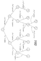
- FIG. 2 is a binary tree representation obtained while implementing the algorithm shown in the flow chart of FIG. 1 ;
- FIG. 3 is a binary tree representation showing the image combinations to be implemented in order to individualize various elements of an integrated circuit
- FIG. 4 is an elevation view of a portion of an integrated circuit
- FIGS. 5 to 15 are views analogous to the view of FIG. 4 while applying distinct test vectors to the inputs of the circuit;
- FIG. 16 is a flow chart of the initial steps of the method of picking out an integrated circuit element from a ternary matrix
- FIG. 17 is a representation of a tree obtained by implementing the method of the invention using a ternary matrix.
- FIG. 18 is a set of processed images of a single portion of an integrated circuit.
- the method of the invention makes it possible to find the exact position of a circuit element on an existing integrated circuit, for example a track, even though the exact layout of the integrated circuit is not known.
- a defective element is located on an image of the circuit or of a portion of the circuit.
- the image is processed to show up only the looked-for element, picking it out relative to the other elements which appear normally on the image of the circuit.
- With the looked-for element picked out in this way in an image of the circuit it is possible using the coordinates of the element on the image to find the position of said element on the integrated circuit proper and thus to apply a measuring device exactly on the circuit element as identified in this way.
- the method of the invention whose algorithm is shown in FIG. 1 comprises three successive stages.
- the first stage 1 consists in using a theoretical circuit diagram of the integrated circuit to build a data structure representative of the theoretical operation of the circuit as a function of a sequence of predefined tests.
- this data structure is in the form of a matrix M whose coefficients are characteristic of the logic states of a set of determined circuit elements while applying the predefined test sequence.
- This first stage integrates prior processing performed on the same matrix M. This processing serves to optimize implementation of the following stages.
- the second stage 2 consists in obtaining a tree of structure that is representative of the processing that needs to be performed on a set of images of the circuit in operation in order to pick out a given element of the circuit in a processed image obtained by combining certain images of the circuit in operation.
- the third stage 3 consists in taking images of the integrated circuit in operation at certain identified instants of the given test sequence and in combining these images in a sequence defined by the predetermined tree structure created as a function of the circuit element that is to be picked out.
- a set is defined of integrated circuit elements that are potentially visible on an image of the circuit in operation.
- these elements are ten in number and that they are formed by tracks formed in the semiconducting material. These tracks are referenced a 1 to a 10 .
- the entire area of the circuit is subdivided into adjacent zones, e.g. formed by adjacent square areas defined by a grid.
- the images obtained in this way of a portion only of the integrated circuit contain a small number of elements that are potentially visible. This number preferably lies in the range 50 to 100 elements per image.
- a computer simulation of its operation is performed in step 12 in order to determine the logic states of the elements a 1 to a 10 while a predetermined test sequence is being input to the integrated circuit.
- This test sequence consists in applying predetermined input values in a sequence that is likewise predetermined.
- the logic states of the elements a 1 to a 10 are stored in vectors b 1 to b 10 .
- Each vector corresponds to a predetermined test instant, and its coefficients are the logic states of the elements a 1 to a 10 at that instant.
- step 12 the computer simulation of the circuit provides a binary matrix M as defined below.
- the vectors b 1 to b 10 constitute the rows.
- the coefficients making up each vector are coefficients that are representative of the logic states of the elements a 1 to a 10 .
- an optional step 14 of converting the binary matrix into a ternary matrix is implemented as a function of the type of analyzer device that is to be used for observing the integrated circuit in operation.
- the analyzer equipment When the analyzer equipment is constituted by a light-emitting microscope, the binary matrix as initially formed is left unchanged and as a result step 14 is omitted. Otherwise, if the analyzer equipment is constituted by a scanning electron microscope, a ternary matrix is formed on the basis of the initially created binary matrix.
- step 14 is described separately after a full description of the algorithm.
- step 16 the elements not present in an image of the region of the circuit under consideration are omitted.
- the columns corresponding to elements that are not potentially visible on the image under consideration are deleted.
- no consideration is given to non-visible elements corresponding to metal tracks that are buried.
- correspondence is used between the names of the elements in the electrical circuit diagram and the numbers of the corresponding polygons in the layout, assuming they are available.
- step 18 the rows and the columns of the matrix are compared with one another. Rows or columns that are identical are deleted in order to avoid duplicate processing later on.
- the vectors corresponding to the various test instants are classified so as to increase their diversity.
- This classification for the purpose of increasing diversity consists in making permutations between the various rows of the matrix.
- Diversity is obtained by classifying the vectors from most significant to least significant and then reorganizing the vectors by alternating more significant vectors and less significant vectors.
- Steps 16 to 20 are optional. In this case, steps 18 and 20 have been omitted.
- stage 2 is performed for creating the binary tree.
- a set of result vectors written r i is built up. These vectors form the nodes of a binary tree as shown in FIG. 2 . Each is constituted by the result of comparing a vector b i of the matrix M with another result vector r j that has already been obtained. Vector comparison is performed coefficient by coefficient by implementing two logic operators, written compa 0 and compa 1 . The truth tables of these two operators compa 0 and compa 1 are given below.
- the result vectors created while implementing the algorithm are obtained by applying one or other of the logic operators compa 0 and compa 1 to one of the earlier result vectors r i and one of the vectors b i of the matrix M as previously built up.
- the result vectors r i have the same number of coefficients as the vectors b 1 to b 10 of the matrix.
- Each result vector r i corresponds to a processed image of the region under consideration of the circuit.
- This processed image is obtained by combining real images as taken of the region under consideration of the circuit at distinct instants of operation while applying the test sequence. These images are combined in a sequence corresponding to the sequence for obtaining the associated result vector, and as described by the structure of the tree.
- the result vectors are created by implementing a recursive algorithm during which each result vector is compared with a vector of the matrix by implementing both of the logic operators compa 0 and compa 1 , and this is continued so long as the result obtained in this way differs from the prior result vector to which the logic operator is applied and so long as there remain vectors in the matrix M that have not been taken into consideration.
- the result vectors r i are placed in a binary tree in which each newly calculated result vector has as its ancestor the vector that was as an operand for calculating it.
- the resulting tree is as shown in FIG. 2 .
- the recursive procedure is initiated in step 22 ( FIG. 1 ) where a first result vector referenced r 0 is taken in which all of its coefficients are equal to 1.
- step 24 The other result vectors are calculated recursively in step 24 until all of the vectors of the matrix M have been taken into consideration or until each of the result vectors obtained can no longer be compared with a vector of the matrix and produce a result differs from the result vector under consideration in the comparison.
- An end test for calculating result vectors is thus performed in step 26 .
- the result vector r 0 is initially compared with the vector b 1 by applying both logic operators compa 1 and compa 0 in order to obtain respective result vectors r 1 and r 2 .
- each result vector r i is set arbitrarily as the integer i used as the index for the result vector.
- the logic operator that is applied is specified in the last column.
- the result vectors r 1 and r 2 are compared with the following vector of the matrix M, i.e. with the vector b 2 by applying the two logic operators compa 0 and compa 1 .
- the two logic operators compa 0 and compa 1 there are created nodes of the tree corresponding to result vectors r 3 and r 4 , which nodes are attached to the node corresponding to result vector r 1 , and similarly nodes corresponding to result vectors r 5 and r 6 which are attached to the node corresponding to result vector r 2 .
- the algorithm continues by comparing result vector r 3 with vector b 3 of the matrix.
- result vector r 3 with vector b 3 of the matrix.
- the coefficients of vectors r 3 and b 3 are analogous, such that the result of comparing them does not lead to a result vector being defined that is not colinear with a result vector already present in the tree that is being created.
- comparison between the vectors r 3 and b 3 is omitted.
- the comparison between the result vector r 3 and the following vector b 4 of the matrix is then performed in order to create result vectors r 7 and r 8 which are obtained respectively by applying the logic operators compa 0 and compa 1 .
- the nodes corresponding to the result vectors r 7 and r 8 are connected to the node corresponding to the result vector r 3 by two branches associated respectively with the logic operators compa 0 and compa 1 .
- result vector pairs r 9 , r 10 and r 11 , r 12 are obtained.
- the details of these calculations are given in Tables 3.2 and 3.3 below.
- result vectors r 9 , r 10 , and r 12 constitute leaves of the tree, whereas result vector r 11 can still be compared pertinently with vectors of the matrix M, since result vector r 11 still has two non-zero coefficients.
- the result vector r 6 is compared with a remaining vector in the matrix M.
- the result of the comparison by logic operator compa 1 is identical to result vector r 6 .
- the result vector that is obtained, written r 13 constitutes a leaf of the tree connected to the node which corresponds to result vector r 6 .
- step 18 This situation could have been avoided by implementing step 18 which, in the example under consideration, was omitted.
- result vectors r 7 , r 8 , r 9 , r 10 , r 12 , and r 13 constitute leaves of the tree, only result vector r 11 is compared with a remaining vector of the tree in order to create vectors r 14 and r 15 which correspond respectively to applying logic operators compa 1 and compa 0 .
- vectors r 14 and r 15 have only one non-zero coefficient each, they constitute leaves of the tree, and as a result comparisons between the vectors of the matrix M and the result vectors r i that are created thereby are terminated.
- a result vector r is created in step 28 .
- the coefficients of this vector are the non-zero coefficients of the set of result vectors that constitute leaves of the tree. By construction, these result vectors r i all have non-zero coefficients in distinct positions.
- the result vector r appears as the bottom row of Table 5 below in which the result vectors r 7 , r 8 , r 9 , r 10 , r 12 , r 13 , r 14 , and r 15 constituting the leaves of the tree are reproduced.
- Image combination is performed on images of the integrated circuit taken at defined instants in the test sequence applied to the circuit.
- image combinations are performed by applying two graphics operators splitby 1 and splitby 0 acting on images in order to compare them pixel to pixel.
- the operator splitby 1 applied to two images of the circuit leads to creating a result image formed by applying the AND function to the corresponding pixels of the two images.
- This operator consists physically in covering the black zones of an image with the corresponding white zones of the other image.
- the operator splitby 0 applied to two images of the circuit leads to a result image being created that is formed by applying the OR function to corresponding pixels in the two images.
- This operator consists physically in covering the white zones of one image with the corresponding black zones of the other image.
- the value of the coefficient i in the vector r is determined and the tree shown in FIG. 2 is used to provide the combination of logic operators that have led to obtaining result vector r i .
- a corresponding graphics operator splitby 0 and splitby 1 is defined. This produces a combination of graphics operators to be applied in a sequence that is the reverse of the sequence in which the logic operators compa 0 and compa 1 were applied from the root of the tree to the leaf under consideration.
- Graphics operator splitby 1 is used on the images as a replacement for logic operator compa 1 as applied to the vectors
- graphics operator splitby 0 is used on the images as a replacement for the logic operator compa 0 applied to the vectors.
- the graphics operators splitby 0 and splitby 1 are applied to images of the circuit in operation taken at identified instants of the test sequence and to images that have already been processed by applying these graphics operators.
- FIG. 3 shows a binary tree corresponding to the tree of FIG. 2 in which the logic operators compa 0 and compa 1 are replaced by graphics operators splitby 0 and splitby 1 .
- These graphics operators are applied to the images of the circuit taken at the instants corresponding to vectors b i of the matrix M.
- the image taken at the instant corresponding to vector b i is written I bi .
- the operand marked by a point corresponds to the processed image obtained by applying one or the other of the operators under consideration at the lower level of the tree.
- the operators splitby 1 and splitby 0 are combined in the order of the path defined by the tree going from the leaf r i under consideration to the root r 0 .
- the image I b0 is a completely black image corresponding to a logic state equal to 1 for all of the nodes of the circuit.
- step 30 for building up the sequence of graphics operators the images needed for applying the above-defined operators in order to individualize a predefined element in an image are acquired in step 32 .
- the images of the portion concerned of the circuit are those stored while applying the predefined sequence of tests, and specifically at the instants corresponding to the vectors b i used in calculating the result vector that corresponds to the circuit element that is to be picked out.
- the images are processed by being digitized so as to reduce their color depth to two colors, namely black and white.
- step 36 the combination of splitby 1 and splitby 0 operators is applied to the images acquired in step 32 and processed in step 34 .
- step 38 the image obtained by applying the operators is displayed.
- the element that is to be picked out appears on its own in this image.
- the coordinates of the element as picked out in this way are extracted in step 40 .
- the image combinations performed consist in masking certain portions of an image by a corresponding portion of another image of different color, and enables undesired circuit elements to be extracted from the final processed image while maintaining on the processed image only the element which is to be picked out.
- the equipment for observing the circuit in operation i.e. in the present case a light-emission microscope, can then be moved to the coordinates taken from the image in order to study accurately the operation of the circuit in the vicinity of said element.
- step 14 of converting the binary matrix of logic states of the circuit into a ternary matrix is performed.
- the coefficients of this ternary matrix can take on three distinct values corresponding to three states of the circuit as observed by the scanning electron microscope.
- the table below gives an example of a matrix of binary states obtained for a test sequence of 24 vectors.
- the 22 circuit elements are labeled with letters A to W.
- FIG. 4 gives an image of the circuit in which there can be seen 22 tracks that are white in color or black in color.
- the tracks are identified by the letters A to W.
- FIGS. 5 to 15 show the images of the circuit in operation as produced by a scanning electron microscope after digital processing for reducing the number of color shades to three, namely black, white, and gray.
- FIGS. 5 to 15 are respective images of the circuit as it appeared at the instants corresponding to the first 11 rows of the ternary matrix given below.
- a ternary tree is created in which the nodes of the tree correspond to result vectors obtained by comparing a prior result vector with one of the vectors of the ternary matrix by applying one of three logic operators compaN, compaB, and compaG, with each of these operators being constructed on the model of the operators compa 1 and compa 0 .
- FIG. 16 is a simplified diagram showing the flow chart of the algorithm for creating the ternary tree by applying the logic operators compaN, compaB, and compaG.
- step 100 the vector 1 of the ternary matrix is considered.
- the vector 1 is compared in step 101 with a first result vector R 0 having all of its coefficients equal to N by applying the logic operator compaN, and with a first result vector R 0 in which all of the coefficients are set to be equal to B by applying the logic operator compaB.
- the vectors R 1 and R 2 created in this way are labeled 104 and 106 .
- a recursive procedure is then implemented at 108 to compare the previously created result vectors with the other vectors of the matrix, applying each of the operators compaN, compaB, and compaG. This procedure is represented by a loop in FIG. 16 .
- a particular element of the circuit is picked out by combining images by applying a combination of graphics operators splitbyN, splitbyB, and splitbyG, these operators corresponding respectively to the logic operators compaN, compaB, and compaG.
- the graphics operators splitbyN, splitbyB, and splitbyG act on images having three color levels (black, white, and gray) to combine two images pixel by pixel for the black, white, and gray elements respectively.
- FIG. 17 The tree created by implementing the algorithm is given in FIG. 17 and the images associated with the main nodes of the tree are given in FIG. 18 .
- the vector 1 is initially compared with the vector R 0 by applying logic operators compaN and compaB so as to give result vectors R 1 and R 2 .
- the calculation of these vectors is given in Table 6 that appears at the end of the description.
- FIG. 18 shows the created images which correspond to result vectors R 1 and R 2 by applying the operators splitbyN and splitbyB respectively to the image of FIG. 5 , and in FIG. 18 these images are designated by reference numbers 202 and 204 .
- result vector R 1 Starting from result vector R 1 , new comparisons are performed to form higher level result vectors R 11 , R 12 , and R 13 , as explained in Table 7.1 which appears at the end of the description.
- result vector R 11 is shown in FIG. 18 where it is referenced 206 .
- This image is formed by applying graphics operator splitbyB to the image 202 and to the image of FIG. 6 which corresponds to vector 2 .
- result vector R 2 In analogous manner, starting from result vector R 2 , higher level result vectors R 21 , R 22 , and R 23 are formed as explained in Table 7.2 which appears at the end of the description.
- result vector R 21 is shown in FIG. 18 where it is given reference 208 .
- This image is formed by applying graphics operator splitbyN to image 204 and the image of FIG. 6 which corresponds to vector 2 .
- the result vector can be further divided, so new comparison steps are performed on the basis of this vector to form higher level result vectors R 121 , R 122 , and R 123 as shown in Table 8.
- the result vectors are made by comparing the vector 3 with the result vector R 12 by applying the three logic operators.
- This image is formed by applying graphics operator splitbyG to the image 208 and to the image of FIG. 7 which corresponds to the vector 3 .
- the element A appears on its own since the only non-zero component of the result vector R 123 is that which appears in the first column corresponding to element A.
Landscapes
- Engineering & Computer Science (AREA)
- Physics & Mathematics (AREA)
- General Physics & Mathematics (AREA)
- General Engineering & Computer Science (AREA)
- Health & Medical Sciences (AREA)
- Microelectronics & Electronic Packaging (AREA)
- Computer Hardware Design (AREA)
- Artificial Intelligence (AREA)
- Evolutionary Computation (AREA)
- Medical Informatics (AREA)
- Tests Of Electronic Circuits (AREA)
- Image Analysis (AREA)
- Semiconductor Integrated Circuits (AREA)
- Design And Manufacture Of Integrated Circuits (AREA)
- Image Processing (AREA)
Applications Claiming Priority (2)
| Application Number | Priority Date | Filing Date | Title |
|---|---|---|---|
| FR00/08337 | 2000-06-28 | ||
| FR0008337A FR2811086B1 (fr) | 2000-06-28 | 2000-06-28 | Procede d'individualisation d'un element de circuit integre |
Publications (2)
| Publication Number | Publication Date |
|---|---|
| US20030174171A1 US20030174171A1 (en) | 2003-09-18 |
| US7190822B2 true US7190822B2 (en) | 2007-03-13 |
Family
ID=8851818
Family Applications (1)
| Application Number | Title | Priority Date | Filing Date |
|---|---|---|---|
| US10/312,632 Expired - Fee Related US7190822B2 (en) | 2000-06-28 | 2001-06-26 | Method for customizing an integrated circuit element |
Country Status (7)
| Country | Link |
|---|---|
| US (1) | US7190822B2 (de) |
| EP (1) | EP1327156B1 (de) |
| AT (1) | ATE274191T1 (de) |
| DE (1) | DE60105044T2 (de) |
| ES (1) | ES2227237T3 (de) |
| FR (1) | FR2811086B1 (de) |
| WO (1) | WO2002001239A1 (de) |
Cited By (14)
| Publication number | Priority date | Publication date | Assignee | Title |
|---|---|---|---|---|
| US20120170830A1 (en) * | 2010-06-14 | 2012-07-05 | Carnegie Mellon University | Method and system for systematic defect identification |
| US9841259B2 (en) | 2015-05-26 | 2017-12-12 | Digital Ally, Inc. | Wirelessly conducted electronic weapon |
| US10013883B2 (en) | 2015-06-22 | 2018-07-03 | Digital Ally, Inc. | Tracking and analysis of drivers within a fleet of vehicles |
| US10074394B2 (en) | 2013-08-14 | 2018-09-11 | Digital Ally, Inc. | Computer program, method, and system for managing multiple data recording devices |
| US10257396B2 (en) | 2012-09-28 | 2019-04-09 | Digital Ally, Inc. | Portable video and imaging system |
| US10271015B2 (en) | 2008-10-30 | 2019-04-23 | Digital Ally, Inc. | Multi-functional remote monitoring system |
| US10272848B2 (en) | 2012-09-28 | 2019-04-30 | Digital Ally, Inc. | Mobile video and imaging system |
| US10521675B2 (en) | 2016-09-19 | 2019-12-31 | Digital Ally, Inc. | Systems and methods of legibly capturing vehicle markings |
| US10757378B2 (en) | 2013-08-14 | 2020-08-25 | Digital Ally, Inc. | Dual lens camera unit |
| US10904474B2 (en) | 2016-02-05 | 2021-01-26 | Digital Ally, Inc. | Comprehensive video collection and storage |
| US10911725B2 (en) | 2017-03-09 | 2021-02-02 | Digital Ally, Inc. | System for automatically triggering a recording |
| US10964351B2 (en) | 2013-08-14 | 2021-03-30 | Digital Ally, Inc. | Forensic video recording with presence detection |
| US11024137B2 (en) | 2018-08-08 | 2021-06-01 | Digital Ally, Inc. | Remote video triggering and tagging |
| US11950017B2 (en) | 2022-05-17 | 2024-04-02 | Digital Ally, Inc. | Redundant mobile video recording |
Families Citing this family (1)
| Publication number | Priority date | Publication date | Assignee | Title |
|---|---|---|---|---|
| US8792835B2 (en) * | 2008-09-22 | 2014-07-29 | Centre National De La Recherche Scientifique | System and method for wirelessly testing integrated circuits |
Citations (6)
| Publication number | Priority date | Publication date | Assignee | Title |
|---|---|---|---|---|
| GB924432A (en) | 1958-08-18 | 1963-04-24 | Thomas Stephen George Seaward | Improved means for the identification of conductors in electric cables or circuits |
| US5570376A (en) * | 1994-10-05 | 1996-10-29 | Sun Microsystems, Inc. | Method and apparatus for identifying faults within a system |
| US5703492A (en) * | 1994-01-10 | 1997-12-30 | Nec Corporation | System and method for fault analysis of semiconductor integrated circuit |
| US5790565A (en) * | 1996-01-12 | 1998-08-04 | Nec Corporation | CMOS integrated circuit failure diagnosis apparatus and diagnostic method |
| FR2786011A1 (fr) | 1998-11-13 | 2000-05-19 | Centre Nat Etd Spatiales | Procede de comparaison d'images enregistrees formees de pixels representant des equipotentielles d'au moins une puce de circuit integre |
| WO2000029953A1 (fr) * | 1998-11-13 | 2000-05-25 | Centre National D'etudes Spatiales (C.N.E.S.) | Procede et installation de localisation rapide d'un defaut dans un circuit integre |
-
2000
- 2000-06-28 FR FR0008337A patent/FR2811086B1/fr not_active Expired - Fee Related
-
2001
- 2001-06-26 ES ES01949534T patent/ES2227237T3/es not_active Expired - Lifetime
- 2001-06-26 AT AT01949534T patent/ATE274191T1/de not_active IP Right Cessation
- 2001-06-26 WO PCT/FR2001/002024 patent/WO2002001239A1/fr not_active Ceased
- 2001-06-26 DE DE60105044T patent/DE60105044T2/de not_active Expired - Lifetime
- 2001-06-26 EP EP01949534A patent/EP1327156B1/de not_active Expired - Lifetime
- 2001-06-26 US US10/312,632 patent/US7190822B2/en not_active Expired - Fee Related
Patent Citations (6)
| Publication number | Priority date | Publication date | Assignee | Title |
|---|---|---|---|---|
| GB924432A (en) | 1958-08-18 | 1963-04-24 | Thomas Stephen George Seaward | Improved means for the identification of conductors in electric cables or circuits |
| US5703492A (en) * | 1994-01-10 | 1997-12-30 | Nec Corporation | System and method for fault analysis of semiconductor integrated circuit |
| US5570376A (en) * | 1994-10-05 | 1996-10-29 | Sun Microsystems, Inc. | Method and apparatus for identifying faults within a system |
| US5790565A (en) * | 1996-01-12 | 1998-08-04 | Nec Corporation | CMOS integrated circuit failure diagnosis apparatus and diagnostic method |
| FR2786011A1 (fr) | 1998-11-13 | 2000-05-19 | Centre Nat Etd Spatiales | Procede de comparaison d'images enregistrees formees de pixels representant des equipotentielles d'au moins une puce de circuit integre |
| WO2000029953A1 (fr) * | 1998-11-13 | 2000-05-25 | Centre National D'etudes Spatiales (C.N.E.S.) | Procede et installation de localisation rapide d'un defaut dans un circuit integre |
Non-Patent Citations (2)
| Title |
|---|
| J D Russell et al., "E-Beam Testing Using Multiple Adjacent Image Processing for Prototype Validation", Microelectronic Engineering, NL, Elsevier Publishers BV., Amsterdam vol. 16, No. 1/04, Mar. 1, 1992, pp. 413-420, XP000245368 ISSN: 0167-9317 le document en entier. |
| K. Nikawa et al., "VLSI Fault Localization Using Electron Beam Voltage Contrast Image.O-Novel Image Acquisition and Localization Method." Japanese Journal of Applied Physics, JP, Publication Office Japanese Journal of Applied Physics. Tokyo, vol. 31, No. 12B, Part 01, Dec. 1, 1992, pp. 4525-4530. XP000415470, ISSN: 0021-4922 le document en entier. |
Cited By (21)
| Publication number | Priority date | Publication date | Assignee | Title |
|---|---|---|---|---|
| US10917614B2 (en) | 2008-10-30 | 2021-02-09 | Digital Ally, Inc. | Multi-functional remote monitoring system |
| US10271015B2 (en) | 2008-10-30 | 2019-04-23 | Digital Ally, Inc. | Multi-functional remote monitoring system |
| US20120170830A1 (en) * | 2010-06-14 | 2012-07-05 | Carnegie Mellon University | Method and system for systematic defect identification |
| US8509517B2 (en) * | 2010-06-14 | 2013-08-13 | Carnegie Mellon University | Method and system for systematic defect identification |
| US11667251B2 (en) | 2012-09-28 | 2023-06-06 | Digital Ally, Inc. | Portable video and imaging system |
| US11310399B2 (en) | 2012-09-28 | 2022-04-19 | Digital Ally, Inc. | Portable video and imaging system |
| US10257396B2 (en) | 2012-09-28 | 2019-04-09 | Digital Ally, Inc. | Portable video and imaging system |
| US10272848B2 (en) | 2012-09-28 | 2019-04-30 | Digital Ally, Inc. | Mobile video and imaging system |
| US10757378B2 (en) | 2013-08-14 | 2020-08-25 | Digital Ally, Inc. | Dual lens camera unit |
| US10885937B2 (en) | 2013-08-14 | 2021-01-05 | Digital Ally, Inc. | Computer program, method, and system for managing multiple data recording devices |
| US10074394B2 (en) | 2013-08-14 | 2018-09-11 | Digital Ally, Inc. | Computer program, method, and system for managing multiple data recording devices |
| US10964351B2 (en) | 2013-08-14 | 2021-03-30 | Digital Ally, Inc. | Forensic video recording with presence detection |
| US10337840B2 (en) | 2015-05-26 | 2019-07-02 | Digital Ally, Inc. | Wirelessly conducted electronic weapon |
| US9841259B2 (en) | 2015-05-26 | 2017-12-12 | Digital Ally, Inc. | Wirelessly conducted electronic weapon |
| US11244570B2 (en) | 2015-06-22 | 2022-02-08 | Digital Ally, Inc. | Tracking and analysis of drivers within a fleet of vehicles |
| US10013883B2 (en) | 2015-06-22 | 2018-07-03 | Digital Ally, Inc. | Tracking and analysis of drivers within a fleet of vehicles |
| US10904474B2 (en) | 2016-02-05 | 2021-01-26 | Digital Ally, Inc. | Comprehensive video collection and storage |
| US10521675B2 (en) | 2016-09-19 | 2019-12-31 | Digital Ally, Inc. | Systems and methods of legibly capturing vehicle markings |
| US10911725B2 (en) | 2017-03-09 | 2021-02-02 | Digital Ally, Inc. | System for automatically triggering a recording |
| US11024137B2 (en) | 2018-08-08 | 2021-06-01 | Digital Ally, Inc. | Remote video triggering and tagging |
| US11950017B2 (en) | 2022-05-17 | 2024-04-02 | Digital Ally, Inc. | Redundant mobile video recording |
Also Published As
| Publication number | Publication date |
|---|---|
| DE60105044D1 (de) | 2004-09-23 |
| FR2811086A1 (fr) | 2002-01-04 |
| US20030174171A1 (en) | 2003-09-18 |
| ES2227237T3 (es) | 2005-04-01 |
| DE60105044T2 (de) | 2005-09-08 |
| EP1327156A1 (de) | 2003-07-16 |
| WO2002001239A1 (fr) | 2002-01-03 |
| FR2811086B1 (fr) | 2002-10-11 |
| ATE274191T1 (de) | 2004-09-15 |
| EP1327156B1 (de) | 2004-08-18 |
Similar Documents
| Publication | Publication Date | Title |
|---|---|---|
| US7190822B2 (en) | Method for customizing an integrated circuit element | |
| DE69127650T2 (de) | Verfahren und Gerät zur Erzeugung von dreidimensionalen graphischen Symbolen | |
| US5757198A (en) | Method and apparatus for detecting an IC defect using charged particle beam | |
| US7756320B2 (en) | Defect classification using a logical equation for high stage classification | |
| Lippmann et al. | Verification of physical designs using an integrated reverse engineering flow for nanoscale technologies | |
| EP1149385A4 (de) | Ic-test programmiersystem zur zuordnung logischer funktionstestdaten von logischen integrierten schaltung zu einer physikalischen darstellung | |
| US5222210A (en) | Method of displaying the state of an artificial neural network | |
| JP3995768B2 (ja) | 不良解析方法及びその装置 | |
| US20100172573A1 (en) | Distinguishing Colors of Illuminated Objects Using Machine Vision | |
| JP4190748B2 (ja) | 半導体不良解析用のcadツール及び半導体不良解析方法 | |
| DE10125331A1 (de) | Vorrichtung und Verfahren zum Erzeugen eines Satzes von Testsequenzen unter Verwendung eines systematischen Füllens | |
| JPH02159681A (ja) | 形状判別システム | |
| CN107102254A (zh) | 一种印制线路板开短路测试方法 | |
| JP3572626B2 (ja) | 検査システム、解析ユニット及び電子デバイスの製造方法 | |
| US6522159B1 (en) | Short-circuit failure analyzing method and apparatus | |
| JPS6115343A (ja) | 集積回路の光学的検査解析方法 | |
| US6816614B1 (en) | Method for comparing recorded pixel images representing equipotential lines of at least an integrated circuit chip | |
| US6819788B2 (en) | Failure analysis method that allows high-precision failure mode classification | |
| JP2000164666A (ja) | 検査システム、解析ユニット及び電子デバイスの製造方法 | |
| US5937269A (en) | Graphics assisted manufacturing process for thin-film devices | |
| JP2920908B2 (ja) | 荷電粒子ビームを用いるic欠陥検出方法及びその装置 | |
| JP3267258B2 (ja) | テストグループ作成装置及びその作成方法 | |
| JPH01277781A (ja) | 集積回路試験装置 | |
| JP2645864B2 (ja) | 集積回路試験装置 | |
| JPH07296013A (ja) | プリント配線板設計装置 |
Legal Events
| Date | Code | Title | Description |
|---|---|---|---|
| AS | Assignment |
Owner name: CENTRE NATIONAL D'ETUDES SPATIALES, FRANCE Free format text: ASSIGNMENT OF ASSIGNORS INTEREST;ASSIGNORS:DESPLATS, ROMAIN;PERDU, PHILIPPE;REEL/FRAME:013595/0933 Effective date: 20021212 |
|
| FEPP | Fee payment procedure |
Free format text: PAYOR NUMBER ASSIGNED (ORIGINAL EVENT CODE: ASPN); ENTITY STATUS OF PATENT OWNER: LARGE ENTITY |
|
| FPAY | Fee payment |
Year of fee payment: 4 |
|
| REMI | Maintenance fee reminder mailed | ||
| LAPS | Lapse for failure to pay maintenance fees | ||
| STCH | Information on status: patent discontinuation |
Free format text: PATENT EXPIRED DUE TO NONPAYMENT OF MAINTENANCE FEES UNDER 37 CFR 1.362 |
|
| STCH | Information on status: patent discontinuation |
Free format text: PATENT EXPIRED DUE TO NONPAYMENT OF MAINTENANCE FEES UNDER 37 CFR 1.362 |
|
| FP | Lapsed due to failure to pay maintenance fee |
Effective date: 20150313 |