US7170189B2 - Semiconductor wafer and testing method therefor - Google Patents
Semiconductor wafer and testing method therefor Download PDFInfo
- Publication number
- US7170189B2 US7170189B2 US11/245,091 US24509105A US7170189B2 US 7170189 B2 US7170189 B2 US 7170189B2 US 24509105 A US24509105 A US 24509105A US 7170189 B2 US7170189 B2 US 7170189B2
- Authority
- US
- United States
- Prior art keywords
- electrode terminal
- detector
- conductor
- semiconductor wafer
- opening
- Prior art date
- Legal status (The legal status is an assumption and is not a legal conclusion. Google has not performed a legal analysis and makes no representation as to the accuracy of the status listed.)
- Active
Links
Images


Classifications
-
- G—PHYSICS
- G01—MEASURING; TESTING
- G01R—MEASURING ELECTRIC VARIABLES; MEASURING MAGNETIC VARIABLES
- G01R31/00—Arrangements for testing electric properties; Arrangements for locating electric faults; Arrangements for electrical testing characterised by what is being tested not provided for elsewhere
- G01R31/28—Testing of electronic circuits, e.g. by signal tracer
- G01R31/2851—Testing of integrated circuits [IC]
- G01R31/2886—Features relating to contacting the IC under test, e.g. probe heads; chucks
- G01R31/2891—Features relating to contacting the IC under test, e.g. probe heads; chucks related to sensing or controlling of force, position, temperature
-
- G—PHYSICS
- G01—MEASURING; TESTING
- G01R—MEASURING ELECTRIC VARIABLES; MEASURING MAGNETIC VARIABLES
- G01R31/00—Arrangements for testing electric properties; Arrangements for locating electric faults; Arrangements for electrical testing characterised by what is being tested not provided for elsewhere
- G01R31/28—Testing of electronic circuits, e.g. by signal tracer
- G01R31/2851—Testing of integrated circuits [IC]
- G01R31/2855—Environmental, reliability or burn-in testing
-
- G—PHYSICS
- G01—MEASURING; TESTING
- G01R—MEASURING ELECTRIC VARIABLES; MEASURING MAGNETIC VARIABLES
- G01R31/00—Arrangements for testing electric properties; Arrangements for locating electric faults; Arrangements for electrical testing characterised by what is being tested not provided for elsewhere
- G01R31/28—Testing of electronic circuits, e.g. by signal tracer
- G01R31/2851—Testing of integrated circuits [IC]
- G01R31/2884—Testing of integrated circuits [IC] using dedicated test connectors, test elements or test circuits on the IC under test
-
- H—ELECTRICITY
- H01—ELECTRIC ELEMENTS
- H01L—SEMICONDUCTOR DEVICES NOT COVERED BY CLASS H10
- H01L2224/00—Indexing scheme for arrangements for connecting or disconnecting semiconductor or solid-state bodies and methods related thereto as covered by H01L24/00
- H01L2224/01—Means for bonding being attached to, or being formed on, the surface to be connected, e.g. chip-to-package, die-attach, "first-level" interconnects; Manufacturing methods related thereto
- H01L2224/02—Bonding areas; Manufacturing methods related thereto
- H01L2224/04—Structure, shape, material or disposition of the bonding areas prior to the connecting process
- H01L2224/06—Structure, shape, material or disposition of the bonding areas prior to the connecting process of a plurality of bonding areas
- H01L2224/0601—Structure
- H01L2224/0603—Bonding areas having different sizes, e.g. different heights or widths
Definitions
- the present invention relates to a semiconductor wafer and a testing method therefore, and in particular to a semiconductor wafer having alignment patterns for conducting tests on the semiconductor wafer and a testing method conducting tests on the semiconductor wafer.
- FIG. 25 shows an enlarged view of a portion of conventional semiconductor wafer. Shown in FIG. 25 is an alignment pattern provided for one semiconductor device.
- an ion probe test on the internal circuitry of the semiconductor device 2 formed on the semiconductor wafer 1 is conducted with a probe card including a number of probes 3 .
- semiconductor devices 2 formed on the semiconductor wafer 1 are tested individually, or a number of semiconductor devices 2 , for example, 2 to 16 semiconductor devices 2 , are tested at a time.
- a number of electrode terminals 4 are formed in each semiconductor device 2 and a pair of adjacent electrode terminals among the electrode terminals 4 is used as an alignment pattern 5 .
- the alignment pattern 5 is used for aligning probes 3 of the probe cards with electrode terminals 4 of the semiconductor device 2 .
- the alignment pattern 5 is used to electrically check to determine whether the probes 3 are properly aligned with the electrode terminals 4 . If they are misaligned, the alignment pattern 5 is used to re-align the probes 3 and the electrode terminals 4 .
- a pair of electrode terminals forming the alignment pattern 5 will be identified as an electrode terminal 9 and a conductor electrode terminal 12 , thereby to distinguish from other electrode terminals 4 that are not included in the alignment pattern 5 .
- the alignment pattern 5 comprises a first electrode terminal section 6 and a second electrode terminal section 7 .
- the first electrode terminal section 6 includes a detector electrode terminal 8 in the form of a ring, an electrode terminal 9 connecting to the internal circuitry of the semiconductor device 2 , and an interconnection 10 connecting the detector electrode terminal 8 with the electrode terminal 9 .
- the second electrode terminal section 7 comprises a conductor electrode terminal 12 that is connected to neither the internal circuit of the semiconductor device 2 or an external terminal.
- the conductor electrode terminal 12 is provided inside and separated from the detector electrode terminal 8 of the first electrode terminal section 6 by a gap 11 .
- the semiconductor device 2 is covered with a protective film, portions of which are removed to provide openings 13 at positions corresponding to the electrode terminals 4 .
- the detector electrode terminal 8 of the first electrode terminal section 6 and the conductor electrode terminal 12 of the second electrode terminal section 7 are exposed in one opening 13 and the electrode terminal 9 of the first electrode terminal section 6 is exposed in another opening 13 .
- a method for using the alignment pattern 5 in a probe test to check to determine whether each probe 3 of a probe card is properly aligned with each electrode terminal 4 of the semiconductor device 2 will be described below.
- the probes 3 of the probe card is brought into contact with the electrode terminals 4 of the semiconductor device 2 . In doing so, one of two probes 3 to which different voltages are applied is brought into contact with the electrode terminal 9 in the first electrode terminal section 6 and the other with the conductor electrode terminal 12 in the second electrode terminal section 7 . Then, current flowing between the probes 3 is monitored.
- both probes 3 are properly positioned with respect to the electrode terminal 9 and the conductor electrode terminal 12 and one of the probes 3 is in contact with only the conductor electrode terminal 12 without departing from the conductor electrode terminal 12 , only internal output signals from the electrode terminal 9 are observed between the probes 3 .
- each probe 3 of the probe card is properly in contact with each electrode terminal 4 of the semiconductor device 2 .
- both of the probes 3 are out of proper alignment with the electrode terminal 9 and the conductor electrode terminal 12 and one of the probe 3 is off the conductor electrode terminal 12 and is in contact with the detector electrode terminal 8 in the first electrode terminal section 6 , both probes 3 are in contact with the first electrode terminal section 6 and signals other than internal output signals from the electrode terminal 9 are observed between the probes 3 in addition to internal output signals.
- FIG. 26 is a schematic diagram showing another conventional alignment pattern.
- the alignment pattern 5 in FIG. 26 is provided in the scribe line 15 between semiconductor devices 2 formed on a semiconductor wafer 1 .
- the alignment pattern 5 comprises three electrode terminals 4 arranged in line and an interconnection 16 interconnecting them.
- the electrode terminal 4 at the center is smaller than the other electrodes at the sides.
- Openings 13 provided in the protective film of the semiconductors 2 have shapes in accordance with the sizes of the side electrodes 4 and the center electrode terminal 4 .
- a method for using the alignment pattern 5 in a probe test will be described below.
- the probes 3 of a prove card are brought into contact with the electrode terminals 4 of a semiconductor device 2 . In doing so, one of three probes 3 is brought into contact with the electrode terminal 4 at the center and the other two probes with the electrode terminals 4 at the sides. Then, electric signals at the center electrode terminal 4 are monitored while a voltage is being applied to the electrode terminals 4 at the sides.
- center probe 3 is not off the center electrode terminal 4 and the tree probes 3 are in contact with the side electrode terminals 4 and the center electrode terminal appropriately, electric signal from the center probe 3 can be observed.
- each probe 3 of the probe card is properly in contact with each electrode terminal 4 of the semiconductor device 2 .
- the size of semiconductor devices is being reduced by miniaturizing the internal circuits of semiconductor devices and reducing the distance between electrode terminals or providing circuit elements directly underneath the electrode terminals or under a location close to the electrode terminals.
- An electrode terminal is exposed in an opening in a nonconductor layer that covers the semiconductor device. If the tip of a probe is out of proper alignment with the electrode terminal, the probe can damage the nonconductor layer around the opening or the load concentrating on the tip of the probe can damage a circuit element under the electrode terminal.
- Using a probe card to conduct an electrical property test or a burn-in test of semiconductor deices on a wafer has the following problems.
- the point of contact of the probe tip on the electrode terminal is gradually displaced from the center of the electrode terminal as the test progresses.
- the probe tip moves off the electrode terminal exposed in the opening in a protective film, that is, the probe tip contacts the protective film around the opening. This can damage the protective film or, in worse cases, affect electrical properties of the device.
- Another problem is that defects undetectable by visual inspections, such as defects that are caused by minute imperfections in a nonconductor layer under an electrode terminal and affect electrical properties can remain at an electrical property testing stage and man-hours for removing the defects is required.
- a load of 5 g applied to the probe tip having a diameter of 20 ⁇ m is equivalent to a pressure of 1600 kg/cm 2 .
- the probe typically made of a tungsten-based material, and the electrode terminal can be oxidized at the point of contact. Consequently, the electric resistance would increase and stable testing would be prohibited.
- An object of the present invention is to improve the efficiency of tests on high-density semiconductor devices having circuit elements directly underneath electrode terminals or under a location close to electrode terminals, that is, electrical property tests and potential defect burn-in screenings of devices on a wafer.
- an object of the present invention is to provide a semiconductor wafer that has alignment patterns to allow bump electrodes and corresponding electrode terminals of semiconductor devices to contact with each other without misalignment in a test using a contactor having multiple bump electrodes, and a testing method therefor.
- the present invention provides a semiconductor wafer on which a plurality of semiconductor devices and alignment patterns are formed, wherein the alignment patterns are formed by an underlying insulating layer, a conducting layer, and upper insulating layer formed on the wafer, a detector electrode terminal and a conductor electrode terminal are formed in the conducting layer, the detector electrode terminal and the conductor electrode terminal are electrically interconnected through a conductor, the upper insulating layer has a detector opening and a conductor opening, the conductor electrode terminal is exposed in the conductor opening, the detector electrode terminal is partially exposed in the detector opening along the inside perimeter of the detector opening, and the underlying layer is exposed in the detector opening in the region other than the region of the detector electrode terminal.
- a through-hole in which the underlying insulating layer is exposed is formed in the detector electrode terminal, the detector opening is formed around the through-hole, and the detector electrode terminal is exposed in the shape of ring along the inside perimeter of the detector opening.
- the through-hole is provided at plurality of locations in the detector electrode terminal in line at regular spacings, the through-holes proportionally varying in size.
- the detector opening is rectangular and a portion of the detector electrode terminal is exposed along one side of the inside perimeter of the detector opening.
- the present invention also provides a semiconductor wafer on which a plurality of semiconductor devices and alignment patterns are formed, wherein the alignment patterns are formed by an underlying insulating layer, a conducting layer, and an upper insulating layer formed on the wafer, a plurality of detector electrode terminals and a plurality of conductor electrode terminals are formed on the conducting layer, the detector electrode terminal and the conductor electrode terminal that make a set are electrically interconnected through a conductor, the upper insulating layer has one detector opening in which the plurality of detector electrode terminals are exposed and a plurality of conductor openings, in each of which one of the plurality of conductor electrode terminals is exposed, the detector opening is rectangular, each of the plurality of detector electrode terminal is partially exposed in the detector opening along each of the sides of the inside perimeter of the detector opening, and the underlying insulating layer is exposed in the detector opening in the region other than the region of the detector electrode terminal.
- the present invention also provides a semiconductor wafer on which a plurality of semiconductor devices and alignment patterns are formed, wherein the alignment patterns are formed by an underlying insulating layer, a conducting layer, and an upper insulating layer, a plurality of detector electrode terminals and a plurality of conductor electrode terminals are formed on the conducting layer, the detector electrode terminal and the conductor electrode terminal making a set are electrically interconnected through a conductor, the upper insulating layer has one detector opening in which the plurality of detector electrode terminals are exposed and a plurality of conductor openings, in each of which one of the plurality of conductor electrode terminals is exposed, the plurality of detector electrode terminals are exposed in the form of spaced coaxial rings in the detector opening, and the underlying insulating layer is exposed in the detector opening in the region other than the region of the detector electrode terminal.
- the conductor electrically connecting the detector electrode terminal and the conductor electrode terminal is the conducting layer.
- a contact hole is formed in the underlying insulating layer of the alignment patterns, an interconnection is provided in the contact hole, and the conductor electrically interconnecting the detector electrode terminal and the conductor electrode terminal is the interconnection.
- the present invention also provides a semiconductor wafer on which a plurality of semiconductor devices and alignment patterns are formed, wherein the alignment patterns are formed by an underlying insulating layer, a conducting layer, and upper insulating layer formed on the wafer, a detector electrode terminal and a conductor electrode terminal are formed in the conducting layer, one of the detector electrode terminal and the conductor electrode terminal is connected to grounding conductor, the other electrode terminal is connected to an input circuit conductor or in a floating state, the upper insulating layer has an opening in which the conductor electrode terminal is exposed and the detector electrode terminal is partially exposed along the inside perimeter of the opening, and the underlying layer is exposed in the opening in the region other than the regions of the conductor electrode terminal and the detector electrode terminal.
- the alignment patterns are formed by an underlying insulating layer, a conducting layer, and upper insulating layer formed on the wafer, a detector electrode terminal and a conductor electrode terminal are formed in the conducting layer, one of the detector electrode terminal and the conductor electrode terminal is connected to grounding conductor, the other electrode
- the present invention also provides a semiconductor wafer testing method for conducting a burn-in test or an electrical property test on a semiconductor wafer having a plurality of semiconductor devices and alignment patterns formed thereon by using a contactor including a plurality of bump electrodes, wherein information about misalignment between electrode terminals of alignment patterns provided at least two locations on the semiconductor wafer and alignment bump electrodes provided in the conductor is electrically detected and monitored during alignment for bringing electrode terminals of the semiconductor devices and the alignment pattern in contact with bump electrodes of the contactor.
- alignment patterns are used when a burn-in test or an electrical property test is conducted on a semiconductor wafer on which semiconductor devices with a highly advanced structure are formed and thereby electrode terminals on the semiconductor wafer can be brought into contact with bump electrodes of a contactor while they are kept in accurate alignment with each other.
- concentration of a load on the electrode terminals can be avoided and therefore high-quality, high-efficiency, and low-cost testing can be accomplished.
- FIG. 1A is a plan view of a semiconductor wafer according to a first embodiment of the present invention.
- FIG. 1B is a plan view of contactors for testing the semiconductor wafer
- FIG. 2 is a plan view of an alignment pattern according to the first embodiment
- FIG. 3 is a cross-sectional view in the direction of arrow A—A of FIG. 1A , showing a semiconductor wafer in proper contact with contactors in the first embodiment;
- FIG. 4 is a cross-sectional view in the direction of arrow A—A of FIG. 1A showing a semiconductor wafer misaligned with and in contact with contactors in the first embodiment;
- FIG. 5 is a flowchart of a process until a test using a monitoring method is completed in an inspection of a wafer according to the first embodiment
- FIG. 6 is a plan view of an alignment pattern according to a second embodiment of the present invention.
- FIG. 7 is a cross-sectional view in the direction of arrow B—B of FIG. 6 ;
- FIG. 8 is a schematic diagram of a circuit for electrically detecting an alignment in the second embodiment
- FIG. 9 is a plan view of an alignment pattern according to a third embodiment of the present invention.
- FIG. 10 is a plan view of an alignment pattern according to a fourth embodiment of the present invention.
- FIG. 11 is a plan view of an alignment pattern according to a fifth embodiment of the present invention.
- FIG. 12 is a plan view of an alignment pattern according to a sixth embodiment of the present invention.
- FIG. 13 is a plan view of an alignment pattern according to a seventh embodiment of the present invention.
- FIG. 14 is a plan view of an alignment pattern according to an eighth embodiment of the present invention.
- FIG. 15 is a plan view of an alignment pattern according to a ninth embodiment of the present invention.
- FIG. 16 is a plan view of an alignment pattern according a tenth embodiment of the present invention.
- FIG. 17 is a plan view of an alignment pattern according to an eleventh embodiment of the present invention.
- FIG. 18 is a plan view of an alignment pattern according to a twelfth embodiment of the present invention.
- FIG. 19 is a plan view showing an arrangement of alignment patterns on a semiconductor wafer according to a thirteenth embodiment of the present invention.
- FIG. 20 is a plan view showing an arrangement of alignment patterns on a semiconductor wafer according to a fourteenth embodiment of the present invention.
- FIG. 21 is a plan view showing an arrangement of alignment patterns on a semiconductor wafer according to a fifteenth embodiment of the present invention.
- FIG. 22 is a plan view showing an arrangement of alignment patterns on a semiconductor wafer according to a sixteenth embodiment of the present invention.
- FIG. 23 is a plan view showing an arrangement of alignment patterns on a semiconductor wafer according to a seventeenth embodiment of the present invention.
- FIG. 24 is a plan view showing an arrangement of alignment patterns on a semiconductor wafer according to eighteenth embodiment of the present invention.
- FIG. 25 is a schematic diagram showing a pattern used for alignment during testing of a semiconductor wafer according to a conventional art.
- FIG. 26 is a schematic diagram showing a pattern used for alignment during testing of a semiconductor wafer according to a conventional art.
- FIG. 1A is a plan view of a semiconductor wafer according to a first embodiment of the present invention
- FIG. 1B is a plan view of a contactor for testing semiconductor devices on the wafer.
- the semiconductor wafer 21 in FIG. 1A includes a number of semiconductor devices 22 , scribe lines 23 for scribes formed between the semiconductors 22 , and alignment patterns 25 formed inside the scribe lines 23 . Electrode terminals 24 for connecting to the external are formed on each semiconductor device 22 .
- the alignment pattern 25 is used in a burn-in test or an electrical property test on the semiconductor wafer 21 .
- more than one alignment pattern 25 is formed in each of the scribe lines 23 intersecting at right angles.
- the contactor 30 in FIG. 1B is a testing tool for conducting burn-in tests or electrical property tests on the semiconductor wafer 21 .
- the contactor 30 has on a substrate a number of bump electrodes 31 for testing some or all of the semiconductor devices 22 at a time. During a test, the contactor 30 is opposed to the semiconductor wafer 21 and the bump electrodes 31 are connected to the electrode terminals 24 and alignment patterns 25 of each semiconductor device 22 .
- the contactor 30 When the contactor 30 is used to test each semiconductor device 2 on the semiconductor wafer 1 , one must make sure that the bump electrodes 31 of the contactor 30 are in contact with and in proper alignment with the electrode terminals 24 of the semiconductor devices 22 .
- While the contactor 30 in FIG. 1 is of rectangular shape, it may be of circular or polygonal shape.
- FIG. 2 is a plan view of an alignment pattern 25 .
- FIGS. 3 and 4 are cross-sectional views in the direction of arrow A—A of FIG. 1 , showing the semiconductor wafer 21 in contact with the contactor 30 .
- FIG. 3 shows the state in which the alignment patterns 25 on the semiconductor wafer 21 are in contact and in proper alignment with the bump electrodes 31 of the contactor 30 .
- FIG. 4 shows a case where the alignment patterns 25 on the semiconductor wafer 21 is in contact but out of alignment with the bump electrodes 31 of the contactor 30 .
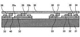
- a conducting layer 33 is formed on an underlying insulating layer 32 , and an upper insulating layer 34 is formed on the conducting layer 33 .
- Each alignment pattern 25 has a detector electrode terminal 38 and a conductor electrode terminal 39 formed by the conducting layer 33 on the underlying insulating layer 32 .
- the detector electrode terminal 38 and the conductor electrode terminal 39 are contiguous regions formed in the conducting layer 33 .
- the conducting layer 33 itself functions as a conductor electrically interconnecting the detector electrode terminal 38 and the conductor electrode terminal 39 .
- a through-hole 40 is provided in the region of the detector electrode terminal 38 in the conducting layer 33 .
- the upper insulating layer 34 is formed over the underlying insulating layer 32 and the conducting layer 33 .
- a rectangular detector opening 35 a and a rectangular conductor opening 35 b are provided in the upper insulating layer 34 .
- the detector electrode terminal 38 is partially exposed in the form of a ring along the inside perimeter of the detector opening 35 a .
- a through-hole 40 is provided in the center of the detector opening 35 a and the underlying insulating layer 32 is exposed in the through-hole 40 where the conducting layer 33 does not exist.
- the conductor electrode terminal 39 is exposed in rectangular shape.
- the bump electrode 31 corresponding to the detector opening 35 a is positioned in the center of the detector opening 35 a , is opposed to the through-hole 40 , where the detector electrode terminal 38 does not exist, and is out of contact with the conducting layer 33 in the region of the detector electrode terminal 38 .
- the bump electrode 31 corresponding to the conductor opening 35 b is in contact with the conducting layer 33 in the region of the conductor electrode terminal 39 .
- the bump electrode 31 corresponding to the detector opening 35 a is not in the center of the detector opening 35 a , faces to the through-hole 40 , is out of the center of the through-hole 40 , and in contact with the conducting layer 33 in the region of the detector electrode terminal 38 .
- the bump electrode 31 corresponding to the conductor opening 35 b is in contact with the conducting layer 33 in the region of the conductor electrode terminal 39 .
- the semiconductor wafer 21 and the contactor 30 are misaligned with each other about the axis perpendicular to the semiconductor wafer 21 if proper alignment is detected at one alignment pattern 25 and misalignment is detected at another alignment pattern 25 .
- the test can be performed with the bump electrodes 31 in alignment and contact with the electrode terminals 24 of the semiconductor devices 22 .
- FIG. 5 is a flowchart of a testing process according to the first embodiment of the present invention.
- the method for testing semiconductor devise 22 on a wafer involves placing the semiconductor wafer 21 under test on a prober table (step 43 ), optically aligning the semiconductor wafer 21 with a contactor 30 (step 44 ), brining the bump electrodes 31 of the contactor 30 into alignment and contact with electrode terminals 24 on the semiconductor wafer 21 (step 45 ), checking the accuracy of alignment between the bump electrodes 31 and the electrode terminals 24 to determine whether the accuracy is acceptable or not (step 46 ), placing the semiconductor wafer 21 and the contactor 30 in a testing machine (step 47 ), adjusting the relative locations of the semiconductor devices 22 and the contactor 30 (step 48 ), and starting an electrical property test on the semiconductor devices 22 (step 49 ).
- the position adjustment step 48 is performed if it is determined at the alignment accuracy determining step 46 that the accuracy of alignment is unacceptable.
- the electrode terminals 24 are realigned with the bump electrodes 31 so that they are placed in proper relative positions.
- the re-alignment operation uses electric signals that are obtained according to the manner in which the alignment patterns and the contactor 30 are connected with each other as information used for re-alignment. Through this position adjustment, accurate alignment between the electrode terminals 24 and the bump electrodes 31 can be accomplished.
- step 45 the process returns to the alignment step 45 for brining the alignment patterns 25 into contact with the contactor 30 .
- step 47 the wafer is placed into the testing machine, and then to the test starting step 49 .
- FIG. 6 is a plan view of an alignment pattern 25 and FIG. 7 is a cross-sectional view in direction of arrow B—B of FIG. 6 .
- the alignment pattern 25 in FIGS. 6 and 7 includes a rectangular conductor electrode terminal 39 formed by a conducting layer on an underlying insulating layer 32 , and a detector electrode terminal 38 surrounding the conductor electrode terminal 39 , except along one side of the conductor electrode terminal 39 .
- a gap is provided between the conductor electrode terminal 39 and the detector electrode terminal 38 .
- the gap may be filled with an insulator film such as SiN.
- An upper insulating layer 34 formed over the underlying insulating layer 32 and the conducting layer 33 has a rectangular opening 35 above the detector electrode terminal 38 and the conductor electrode terminal 39 .
- the entire conductor electrode terminal 39 is exposed in the opening 35 and the detector electrode terminal 38 is partially exposed along the internal perimeter of the opening 35 .
- the underlying insulting layer 32 is also exposed in the regions where neither the conductor electrode terminal 39 nor the detector electrode terminal 38 is provided.
- the detector electrode terminal 38 is connected to a grounding conductor 55 and the conductor electrode terminal 39 is connected to an input circuit conductor 56 .
- the conductor electrode terminal 39 may be in a floating state.
- the conductor electrode terminal 39 may be connected to the grounding conductor 55
- the detector electrode terminal 38 may be connected to the input circuit conductor 56 .
- the conductor electrode terminal 39 may be an electrode terminal 24 of a semiconductor device 22 , or the conductor electrode terminal 39 may be provided separately. While the conductor terminal 39 is of a rectangular shape, the shape of the conductor terminal 39 is not limited to a rectangle. Furthermore, the upper insulating layer 34 may be extended to the position at which it contacts one end of the conductor electrode terminal 39 at the open side of the detector electrode terminal 38 . This reduces depressions in the surface of the alignment pattern 5 .
- FIG. 8 is a schematic diagram showing an example of a circuit for electrically detecting alignment between the semiconductor wafer 21 and the contactor 30 .
- FIG. 9 is a plan view of an alignment pattern 25 .
- the alignment pattern 25 in FIG. 9 includes a rectangular conductor electrode terminal 39 formed by a conducting layer on an underlying insulating layer 32 , and a detector electrode terminal 38 opposed to and separated by a gap from one end of he conductor electrode terminal 39 .
- An upper insulating layer 34 provided over the underlying insulating layer 32 and the conducing layer 33 has an opening 35 above the detector electrode terminal 38 and the conductor electrode terminal 39 .
- the opening 35 a portion of the conductor electrode terminal 39 and a portion of the detector electrode terminal 38 are exposed from one of the sides of the perimeter of the opening 35 , the portion of the detector electrode terminal 38 is exposed along one of the sides of the perimeter of the opening 35 , and the underlying insulating layer 32 is exposed in the regions where neither the conductor electrode terminal 39 nor the detector electrode terminal 38 is provided.
- the exposed area of the conductor electrode terminal 39 is well larger than the exposed area of the detector electrode terminal 38 .
- the detector electrode terminal 38 is connected to a grounding conductor 55 and the conductor electrode terminal 39 is connected to an input circuit conductor 56 . Misalignment between the semiconductor wafer 21 and a contactor 30 is electrically detected by applying a voltage to an internal circuit during an alignment step.
- the conductor electrode terminal 39 may be in a floating state.
- a pair of alignment patterns 25 having different layouts are used.
- the conductor electrode terminal 39 maybe disposed in its right-hand part and the detector electrode terminal 38 in its left-hand part.
- the conductor electrode terminal 39 maybe disposed in its left-hand part and the detector electrode terminal 38 in the right-hand part.
- Determination as to whether or not the semiconductor wafer 21 is in proper alignment with the contactor 30 is made in the same manner as the second embodiment.
- FIG. 10 is a plan view oft he alignment pattern 25 .
- the alignment pattern 25 in FIG. 10 includes a rectangular conductor electrode terminal 39 formed by a conducting layer on an underlying insulting layer 32 and a detector electrode terminal 38 which surrounds the conductor electrode terminal 39 with its sides opposed to the sides of the conductor electrode terminal 39 and is separated from the conductor electrode terminal 39 by a gap.
- An upper insulating layer 34 formed over the underlying insulating layer 32 and the conducting layer 33 has an opening 35 above the detector electrode terminal 38 and the conductor electrode terminal 39 .
- the opening 35 the entire conductor electrode terminal 39 is exposed, the detector electrode terminal 38 is partially exposed in the form of a ring along the inside perimeter of the opening 35 , and the underlying insulating layer 32 is exposed in the regions where the conductor electrode terminal 39 or the detector electrode terminal 38 is not provided.
- the detector electrode terminal 38 is connected to a grounding conductor 55 and the conductor electrode terminal 39 is connected to an input circuit conductor 56 .
- the conductor electrode terminal 39 can be in a floating state.
- Determination as to whether the semiconductor wafer 21 is in proper alignment with a contactor 30 is made in the same manner as the second embodiment.
- FIG. 11 is a plan view of an alignment pattern 25 .
- the alignment pattern 25 in FIG. 11 includes a detector electrode terminal 38 and a conductor electrode terminal 39 formed on an underlying insulating layer 32 .
- the detector electrode terminal 38 and the conductor electrode terminal 39 are formed as a continuous conducting layer 33 .
- the conducting layer 33 itself functions as a conductor electrically interconnecting the detector electrode terminal 38 with the conductor electrode terminal 39 .
- An upper insulating layer 34 provided over underlying insulating layer 32 and the conducting layer 33 has a rectangular detector opening 35 a and a rectangular conductor opening and 35 b.
- the detector electrode terminal 38 of the conducting layer 33 is partially exposed at only one of the sides of the opening 35 a and the underlying insulating layer 32 is exposed in the remaining regions except in the region where the detector electrode terminal 38 is formed.
- the conductor opening 35 b a rectangular region of the conductor electrode terminal 39 of the conducting layer 33 is exposed.
- Determination as to whether the semiconductor wafer 21 is in proper alignment with a contactor 30 is made in the same manner as the first embodiment.
- FIG. 12 is a plan view of an alignment pattern 25 .
- the alignment pattern 25 in FIG. 12 includes a detector electrode terminal 38 and a conductor electrode terminal 39 formed on an underlying insulating layer 32 .
- the detector electrode terminal 38 and the conductor electrode terminal 39 are separately formed in discontiguous regions in a conducting layer 33 .
- An underlying layer interconnection 60 is provided in a contact hole in the underlying insulating layer 32 , and the detector electrode terminal 38 and the conductor electrode terminal 39 are interconnected through the underlying-layer interconnection 60 which forms a conductor.
- An upper insulating layer 34 provided over the underlying insulating layer 32 and the conducting layer 33 has a rectangular detector opening 35 a and a rectangular conductor opening 35 b.
- the detector electrode terminal 38 is partially exposed in the form of a ring along the inside perimeter of the detector opening 35 a .
- a through-hole 40 is provided in the center of the detector opening 35 a and the underlying insulating layer 32 is exposed through the through-hole 40 in which the conducting layer 33 does not exist.
- the conductor electrode terminal 39 is exposed in rectangular shape.
- Determination as to whether the semiconductor wafer 21 is in proper alignment with a contactor 30 is made in the same manner as the first embodiment.
- FIG. 13 is a plan view of an alignment pattern 25 .
- the alignment pattern 25 in FIG. 13 includes a detector electrode terminal 38 and a conductor electrode terminal 39 formed on an underlying insulating layer 32 .
- the detector electrode terminal 38 and the conductor electrode terminal 39 are separate regions formed in a continuous conducting layer 33 .
- the conducting layer 33 itself functions as a conductor electrically interconnecting the detector electrode terminal 38 and the conductor electrode terminal 39 .
- a through-hole 40 is provided in the region of the detector electrode terminal 38 in the conducting layer 33 .
- An upper insulating layer 34 provided over the underlying insulating layer 32 and the conducting layer 33 has rectangular detector and conductor openings 35 a and 35 b.
- the detector electrode terminal 38 is partially exposed in the form of a ring along the inside perimeter of the detector opening 35 . Also in the detector opening 35 a , the underlying insulating layer 32 is exposed through a through-hole 40 in which the conducting layer 33 does not exist. In the conductor opening 35 b , the conductor electrode terminal 39 is exposed in rectangular shape.
- a protrusion 61 is provided in the center of the detector opening 35 a .
- the protrusion 61 is spaced apart from the detector electrode terminal 38 .
- the protrusion 61 maybe formed of the upper insulating layer 34 , the conducting layer 33 or another material.
- the height of the protrusion 61 is the same as that of the conducting layer 33 so that the protrusion 61 can be brought into good contact with a bump electrode 31 of a contactor 30 .
- Determination as to whether the semiconductor wafer 21 is in proper alignment with the contactor 30 is made in the same manner that in the first embodiment.
- FIG. 14 is a plan view of an alignment pattern 25 .
- the alignment pattern 25 in FIG. 14 includes a detector electrode terminal 38 and a conductor electrode terminal 39 formed on an underlying insulating layer 32 .
- the detector electrode terminal 38 and the conductor electrode terminal 39 are separate regions formed in a continuous conducting layer 33 .
- the conducting layer 33 itself functions as a conductor interconnecting the detector electrode terminal 38 and the conductor electrode terminal 39 .
- a number of through holes 40 are provided in the conducting layer 33 in the region of the detector electrode terminal 38 .
- the through-holes 40 are rectangular and proportionally vary in size.
- the center of each through-hole 40 is substantially aligned with the center line of the opening 35 .
- An upper insulating layer 34 provided over the underlying insulting layer 32 and the conducting layer 33 has rectangular detector and conductor openings 35 a and 35 b.
- the detector electrode terminal 38 is partially exposed in the form of a ring along the inside perimeter of the detector opening 35 a . Also in the detector opening 35 a , the underlying insulating layer 32 is exposed through the through-holes 40 in which the conducing layer 33 does not exist. In the conductor opening 35 b , the conductor electrode terminal 39 is exposed in rectangular shape.
- Determination as to whether the semiconductor wafer 21 is in proper alignment with a contactor 30 is made in the same manner as that in the first embodiment.
- the magnitude of misalignment, if any, between the semiconductor wafer 21 and the contactor 30 can be known by placing the bump electrodes 31 of the contactor 30 in the multiple through-holes 40 .
- the magnitude of the misalignment can be estimated from the size of the largest of the through-holes 40 in which the detector electrode terminal 38 contact the bump electrode 31 .
- FIG. 15 is a plan view of an alignment pattern 25 .
- the alignment pattern 25 in FIG. 15 includes multiple detector electrode terminals 38 and multiple conductor electrode terminals 39 formed on an underlying insulating layer 32 .
- the detector electrode terminals 38 and the conductor electrode terminals 39 have their respective regions formed in a continuous conducting layer 33 .
- An interconnection 62 formed in the conducting layer functions as a conductor connecting each conductor electrode terminal 39 with each detector electrode terminal 38 .
- four pairs comprising a conductor electrode terminal 39 and a detector electrode terminal 38 are provided in a substantially straight line.
- the detector electrode terminals 38 are spatially separated from each other and the conductor electrode terminals 39 are also spatially separated from each other.
- An upper insulating layer 34 provided over the underlying layer 32 and the conducting layer 33 has one rectangular detector opening 35 a and multiple rectangular conductor openings 35 b.
- the detector electrode terminals 38 are exposed. Each detector electrode terminal 38 is partially exposed along each side of the inside perimeter of the detector opening 35 a and the underlying insulating layer 32 is exposed in the region in the detector opening 35 a where the detector electrode terminals 38 are not formed. In each of the multiple conductor openings 35 b , a conductor electrode terminal 39 is exposed.
- Determination as to whether or not the semiconductor wafer 21 is in proper alignment with a contactor 30 is made in the same manner as the first embodiment.
- the direction of misalignment, if any, between the semiconductor wafer 21 and the contactor 30 can also be known by placing the bump electrodes 31 of the contactor 30 in the detector and the conductor openings 35 a and 35 b.
- FIG. 16 is a plan view of an alignment pattern 25 .
- the alignment pattern 25 in FIG. 16 includes three pairs of a detector electrode terminal 38 and a conductor electrode terminal 39 formed on an underlying insulating layer 32 .
- An upper insulating layer 34 provided over the underlying insulating layer 32 has one rectangular detector opening 35 a and a number of conductor openings 35 b.
- the detector electrode terminals 38 are exposed in the detector opening 35 a in the form of rings along the perimeter of the detector opening 35 a .
- a through-hole 40 is provided in the center of the detector opening 35 a and the detector electrode terminals 38 are provided coaxially and separated from each other by a gap.
- the underlying insulating layer 32 is exposed in the region where the detector electrode terminals 38 are not provided.
- the pair comprising the outermost detector electrode terminal 38 and a conductor electrode terminal 39 is formed as a continuous conducting layer 33 comprising the outermost detector electrode terminal 38 and a conductor electrode terminal 39 .
- the conductor electrode terminal 39 is exposed in rectangular shape in its corresponding conductor opening 35 b.
- the conductor electrode terminal 39 of each of the other two pairs is exposed in rectangular shape in the corresponding conductor opening 35 b and connected to the middle or the innermost detector electrode terminal 38 through an interconnection 60 in the underlying layer as a conducting means.
- Determination as to whether the semiconductor wafer 21 is in proper alignment with a contactor 30 is made in the same manner as the first embodiment.
- the magnitude of misalignment, if any, between the semiconductor wafer 21 and the contactor 30 can be known by placing bump electrodes 31 of the contactor 30 in the detector opening 35 a and the conductor openings 35 b.
- FIG. 17 is a plan view of an alignment pattern 25 .
- the alignment pattern 25 in FIG. 17 includes two pairs of a detector electrode terminal 38 and a conductor electrode terminal 39 formed on an underlying insulating layer 32 .
- Each the pair of detector electrode terminals 38 and the pair of conductor electrode terminals 39 is formed by a continuous conducting layer 33 .
- An upper insulating layer 34 provided on the underlying insulating layer 32 has one rectangular detector opening 35 a and multiple rectangular conductor openings 35 b.
- each conductor electrode terminal 39 is exposed in rectangular shape.
- the two pairs of detector and conductor electrode terminals 38 and 39 are provided symmetrically.
- Determination as to whether the semiconductor wafer 21 is in proper alignment with a contactor 30 is made in the same manner as in the first embodiment.
- the direction of misalignment of the semiconductor wafer 21 with the contactor 30 can be known by placing the bump electrodes 31 of the contactor 30 in the detector opening 35 a and the conductor opening 35 b.
- FIG. 18 is a plan view of an alignment pattern 25 .
- the alignment pattern 25 in FIG. 18 includes four pairs of a detector electrode terminal 38 and a conductor electrode terminal 39 formed on an underlying insulating layer 32 . Each pair of the detector electrode terminal 38 and the conductor electrode terminal 39 is formed in a continuous conducting layer 33 .
- An upper insulating layer 34 provided over the underlying insulating layer 32 has one rectangular detector opening 35 a and multiple rectangular conductor openings 35 b.
- the detector electrode terminal 38 of one pair is exposed at each of the four sides of the opening and the underlying insulating layer 32 is exposed in the region except of the detector electrode terminal 38 .
- the conductor electrode terminal 39 is exposed in rectangular shape. The four pairs of detector electrode and conductor electrode terminals 38 and 39 make the shape of a cross.
- Determination as to whether the semiconductor wafer 21 is in proper alignment with a contactor 30 is made in the same way as in the first embodiment.
- the direction of misalignment of the semiconductor wafer 21 with the contactor 30 can be known by placing the bump electrodes 31 of the contactor 30 in the detector electrode opening 35 a and the conductor electrode openings 35 b.
- a bump electrode 31 of the contactor 30 is in contact with a detector electrode terminal 38 at the lower part of FIG. 17 , electricity is conducted between the bump electrode 31 in contact with the conductor electrode terminal 39 formed in the same conducting layer 33 in which the detector electrode terminal 38 is formed and the bump electrode 31 in contact with the detector electrode terminal 38 .
- FIG. 19 is a plan view showing an arrangement of alignment patterns 25 on a semiconductor wafer 21 .
- an alignment pattern 25 is placed in at least two locations in strait-line areas 65 , other than the intersections of scribe lines 23 , within the area in which semiconductor devices 22 are placed.
- This arrangement of alignment patterns 25 on the semiconductor wafer 21 enables the semiconductor wafer 21 to be aligned with a contactor 30 with high accuracy.
- FIG. 20 is a plan view showing an arrangement of alignment patterns 25 on a semiconductor wafer 21 .
- an alignment pattern 25 is placed in at least two intersections 66 of scribe lines 23 within a placement region of semiconductor devices 22 .
- This arrangement of alignment patterns 25 on the semiconductor wafer 21 enables the semiconductor wafer 21 to be aligned with a contactor 30 with high accuracy.
- FIG. 21 is a plan view showing an arrangement of alignment patterns 25 on a semiconductor wafer 21 .
- the alignment patterns 25 are placed in positions at a certain distance from the intersection 66 of scribe lines 23 within the placement region of semiconductor devices 22 .
- a pair of alignment patterns 25 may be placed at an angle of 180 degrees symmetrically about a certain point.
- a number of alignment patterns 25 may be provided in scribe lines 23 at intervals of 90 degrees about a certain point in the form of the character T or a cross.
- Such a set of alignment patterns 25 is placed in at least two intersections of scribe lines 23 .
- This arrangement of such sets of alignment patterns 25 on the semiconductor wafer 21 enables the semiconductor wafer 21 to be aligned with a contactor 30 with high accuracy.
- misalignment directions and magnitudes can be determined. For example, if the alignment pattern 25 shown in FIG. 14 is provided in four directions, misalignment directions and magnitudes can be determined.
- FIG. 22 is a plan view showing an arrangement of alignment patterns 25 on a semiconductor wafer 21 .
- an alignment pattern 25 is provided in at least two semiconductor devices 22 within the placement region of semiconductor devices 22 .
- This arrangement of alignment patterns 25 on the semiconductor wafer 21 enables the semiconductor wafer 21 to be aligned with a contactor 30 with a high accuracy.
- FIG. 23 is a plan view showing an arrangement of alignment patterns 25 on a semiconductor wafer 21 .
- an alignment pattern 25 is placed in at least two locations in the peripheral edge margin 67 where no semiconductor device 22 is provided.
- This arrangement of alignment patterns 25 on the semiconductor wafer 21 enables the semiconductor wafer 21 to be aligned with a contactor 30 with high accuracy.
- FIG. 24 is a plan view showing an arrangement of alignment patterns 25 on a semiconductor wafer 21 .
- an alignment pattern 25 is placed in at least two substantially opposed two locations in a straight-line area of a scribe line 23 within the semiconductor device 22 layout area.
- an alignment pattern 25 may be placed in at least two intersections 66 of scribe lines or at least two locations in the peripheral edge margin 67 .
- This arrangement of alignment patterns 25 on the semiconductor wafer 21 enables the semiconductor wafer 21 to be aligned with a contactor 30 with high accuracy.
- the semiconductor wafer and testing method thereof according to the present invention are effective at improving the quality and efficiency of tests of semiconductor devices formed on a semiconductor wafer.
Abstract
Description
- 1. Japanese Patent Laid-Open No. 5-343487
- 2. Japanese Patent Laid-Open No. 6-045419
Claims (18)
Applications Claiming Priority (2)
| Application Number | Priority Date | Filing Date | Title |
|---|---|---|---|
| JP2004331293A JP4570446B2 (en) | 2004-11-16 | 2004-11-16 | Semiconductor wafer and inspection method thereof |
| JP2004-331293 | 2004-11-16 |
Publications (2)
| Publication Number | Publication Date |
|---|---|
| US20060103408A1 US20060103408A1 (en) | 2006-05-18 |
| US7170189B2 true US7170189B2 (en) | 2007-01-30 |
Family
ID=36385617
Family Applications (1)
| Application Number | Title | Priority Date | Filing Date |
|---|---|---|---|
| US11/245,091 Active US7170189B2 (en) | 2004-11-16 | 2005-10-07 | Semiconductor wafer and testing method therefor |
Country Status (4)
| Country | Link |
|---|---|
| US (1) | US7170189B2 (en) |
| JP (1) | JP4570446B2 (en) |
| CN (1) | CN100461381C (en) |
| TW (1) | TW200617410A (en) |
Cited By (3)
| Publication number | Priority date | Publication date | Assignee | Title |
|---|---|---|---|---|
| US20050258854A1 (en) * | 2004-05-18 | 2005-11-24 | Samsung Electronics Co., Ltd. | Probe pad, substrate having a semiconductor device, method of testing a semiconductor device and tester for testing a semiconductor device |
| US20070090851A1 (en) * | 2005-05-17 | 2007-04-26 | Samsung Electronics Co., Ltd. | Probe sensing pads and methods of detecting positions of probe needles relative to probe sensing pads |
| US20100134124A1 (en) * | 2006-07-06 | 2010-06-03 | Au Optronics Corp. | Misalignment detection devices |
Families Citing this family (8)
| Publication number | Priority date | Publication date | Assignee | Title |
|---|---|---|---|---|
| JP2007335550A (en) * | 2006-06-14 | 2007-12-27 | Seiko Instruments Inc | Semiconductor device |
| JP4995495B2 (en) * | 2006-06-16 | 2012-08-08 | セイコーインスツル株式会社 | Semiconductor device |
| JP4712641B2 (en) * | 2006-08-09 | 2011-06-29 | 富士通セミコンダクター株式会社 | Semiconductor wafer and test method thereof |
| KR100892262B1 (en) * | 2007-06-27 | 2009-04-09 | 세크론 주식회사 | Computing system for operation ratio of probing tester and computing method thereby |
| EP2246708A1 (en) * | 2009-04-30 | 2010-11-03 | Micronas GmbH | Method for producing a defect map of individual components, in particular semiconductor components, on a carrier, in particular a semiconductor wafer |
| IT1397222B1 (en) * | 2009-12-30 | 2013-01-04 | St Microelectronics Srl | METHOD TO CHECK THE CORRECT POSITION OF TEST PROBES ON TERMINATIONS OF ELECTRONIC DEVICES INTEGRATED ON SEMICONDUCTOR AND ITS ELECTRONIC DEVICE. |
| US8838408B2 (en) | 2010-11-11 | 2014-09-16 | Optimal Plus Ltd | Misalignment indication decision system and method |
| CN104181448A (en) * | 2014-08-13 | 2014-12-03 | 华进半导体封装先导技术研发中心有限公司 | Silicon through hole patch board wafer testing system and method |
Citations (12)
| Publication number | Priority date | Publication date | Assignee | Title |
|---|---|---|---|---|
| JPH05343487A (en) | 1992-06-04 | 1993-12-24 | Nec Corp | Semiconductor integrated circuit device |
| JPH0645419A (en) | 1992-07-21 | 1994-02-18 | Hitachi Ltd | Semiconductor device |
| US5321277A (en) * | 1990-12-31 | 1994-06-14 | Texas Instruments Incorporated | Multi-chip module testing |
| US6087719A (en) * | 1997-04-25 | 2000-07-11 | Kabushiki Kaisha Toshiba | Chip for multi-chip semiconductor device and method of manufacturing the same |
| US6133054A (en) * | 1999-08-02 | 2000-10-17 | Motorola, Inc. | Method and apparatus for testing an integrated circuit |
| US6133582A (en) * | 1998-05-14 | 2000-10-17 | Lightspeed Semiconductor Corporation | Methods and apparatuses for binning partially completed integrated circuits based upon test results |
| US6380555B1 (en) * | 1999-12-24 | 2002-04-30 | Micron Technology, Inc. | Bumped semiconductor component having test pads, and method and system for testing bumped semiconductor components |
| US20020164840A1 (en) * | 2001-05-01 | 2002-11-07 | Industrial Technology Research Institute | Method for forming a wafer level package incorporating a multiplicity of elastomeric blocks and package formed |
| US20030122246A1 (en) * | 2001-12-31 | 2003-07-03 | Mou-Shiung Lin | Integrated chip package structure using silicon substrate and method of manufacturing the same |
| US6781150B2 (en) * | 2002-08-28 | 2004-08-24 | Lsi Logic Corporation | Test structure for detecting bonding-induced cracks |
| US6781365B2 (en) * | 1999-04-06 | 2004-08-24 | Micron Technology, Inc. | Conductive material for integrated circuit fabrication |
| US6881597B2 (en) * | 2001-01-22 | 2005-04-19 | Renesas Technology Corp. | Method of manufacturing a semiconductor device to provide a plurality of test element groups (TEGs) in a scribe region |
Family Cites Families (4)
| Publication number | Priority date | Publication date | Assignee | Title |
|---|---|---|---|---|
| JPS56114349A (en) * | 1980-02-15 | 1981-09-08 | Chiyou Lsi Gijutsu Kenkyu Kumiai | Detecting method for displacement in testing stage of wafer |
| JPS63128636A (en) * | 1986-11-18 | 1988-06-01 | Nec Corp | Semiconductor integrated circuit device |
| AU634334B2 (en) * | 1990-01-23 | 1993-02-18 | Sumitomo Electric Industries, Ltd. | Packaging structure and method for packaging a semiconductor device |
| JPH09213759A (en) * | 1996-01-30 | 1997-08-15 | Sony Corp | Semiconductor device |
-
2004
- 2004-11-16 JP JP2004331293A patent/JP4570446B2/en not_active Expired - Fee Related
-
2005
- 2005-10-07 US US11/245,091 patent/US7170189B2/en active Active
- 2005-11-09 TW TW094139264A patent/TW200617410A/en unknown
- 2005-11-11 CN CNB2005101250113A patent/CN100461381C/en not_active Expired - Fee Related
Patent Citations (12)
| Publication number | Priority date | Publication date | Assignee | Title |
|---|---|---|---|---|
| US5321277A (en) * | 1990-12-31 | 1994-06-14 | Texas Instruments Incorporated | Multi-chip module testing |
| JPH05343487A (en) | 1992-06-04 | 1993-12-24 | Nec Corp | Semiconductor integrated circuit device |
| JPH0645419A (en) | 1992-07-21 | 1994-02-18 | Hitachi Ltd | Semiconductor device |
| US6087719A (en) * | 1997-04-25 | 2000-07-11 | Kabushiki Kaisha Toshiba | Chip for multi-chip semiconductor device and method of manufacturing the same |
| US6133582A (en) * | 1998-05-14 | 2000-10-17 | Lightspeed Semiconductor Corporation | Methods and apparatuses for binning partially completed integrated circuits based upon test results |
| US6781365B2 (en) * | 1999-04-06 | 2004-08-24 | Micron Technology, Inc. | Conductive material for integrated circuit fabrication |
| US6133054A (en) * | 1999-08-02 | 2000-10-17 | Motorola, Inc. | Method and apparatus for testing an integrated circuit |
| US6380555B1 (en) * | 1999-12-24 | 2002-04-30 | Micron Technology, Inc. | Bumped semiconductor component having test pads, and method and system for testing bumped semiconductor components |
| US6881597B2 (en) * | 2001-01-22 | 2005-04-19 | Renesas Technology Corp. | Method of manufacturing a semiconductor device to provide a plurality of test element groups (TEGs) in a scribe region |
| US20020164840A1 (en) * | 2001-05-01 | 2002-11-07 | Industrial Technology Research Institute | Method for forming a wafer level package incorporating a multiplicity of elastomeric blocks and package formed |
| US20030122246A1 (en) * | 2001-12-31 | 2003-07-03 | Mou-Shiung Lin | Integrated chip package structure using silicon substrate and method of manufacturing the same |
| US6781150B2 (en) * | 2002-08-28 | 2004-08-24 | Lsi Logic Corporation | Test structure for detecting bonding-induced cracks |
Cited By (7)
| Publication number | Priority date | Publication date | Assignee | Title |
|---|---|---|---|---|
| US20050258854A1 (en) * | 2004-05-18 | 2005-11-24 | Samsung Electronics Co., Ltd. | Probe pad, substrate having a semiconductor device, method of testing a semiconductor device and tester for testing a semiconductor device |
| US7616020B2 (en) * | 2004-05-18 | 2009-11-10 | Samsung Electronics Co., Ltd. | Probe pad, substrate having a semiconductor device, method of testing a semiconductor device and tester for testing a semiconductor device |
| US20070090851A1 (en) * | 2005-05-17 | 2007-04-26 | Samsung Electronics Co., Ltd. | Probe sensing pads and methods of detecting positions of probe needles relative to probe sensing pads |
| US7612573B2 (en) | 2005-05-17 | 2009-11-03 | Samsung Electronics Co., Ltd. | Probe sensing pads and methods of detecting positions of probe needles relative to probe sensing pads |
| US20100134124A1 (en) * | 2006-07-06 | 2010-06-03 | Au Optronics Corp. | Misalignment detection devices |
| US8426987B2 (en) * | 2006-07-06 | 2013-04-23 | Au Optronics Corp. | Misalignment detection devices |
| US8816707B2 (en) | 2006-07-06 | 2014-08-26 | Au Optronics Corp. | Misalignment detection devices |
Also Published As
| Publication number | Publication date |
|---|---|
| JP4570446B2 (en) | 2010-10-27 |
| CN1776898A (en) | 2006-05-24 |
| US20060103408A1 (en) | 2006-05-18 |
| JP2006147601A (en) | 2006-06-08 |
| TW200617410A (en) | 2006-06-01 |
| CN100461381C (en) | 2009-02-11 |
Similar Documents
| Publication | Publication Date | Title |
|---|---|---|
| US7170189B2 (en) | Semiconductor wafer and testing method therefor | |
| US10746788B2 (en) | Sensing structure of alignment of a probe for testing integrated circuits | |
| JP4898139B2 (en) | Probe pad, substrate on which semiconductor element is mounted, and semiconductor element inspection method | |
| KR20040004002A (en) | Probe needle fixing apparatus and method for semiconductor device test equipment | |
| US9823300B2 (en) | Process for controlling the correct positioning of test probes on terminations of electronic devices integrated on a semiconductor and corresponding electronic device | |
| KR20030036068A (en) | Semiconductor device, its manufacturing process, and its inspecting method | |
| KR100652421B1 (en) | Doughnut type parallel probe card and method of wafer testing using the same | |
| KR910007510B1 (en) | Semiconductor device | |
| JPH09107011A (en) | Semiconductor device and aligning method thereof | |
| KR102195561B1 (en) | Electrical connection device | |
| KR102257278B1 (en) | Electrical connection device | |
| KR101227547B1 (en) | Probe card | |
| JP3214420B2 (en) | Film carrier type semiconductor device, inspection probe head, and alignment method | |
| US11372024B2 (en) | Probe card test apparatus | |
| TW201432269A (en) | Probe card, inspection apparatus and inspection method | |
| JP2010098046A (en) | Probe card and method for manufacturing semiconductor device | |
| JP2004356597A (en) | Inspection method of semiconductor chip, and probe card used for the same | |
| JPS6167238A (en) | Semiconductor device | |
| JP2012204626A (en) | Semiconductor device and semiconductor device manufacturing method | |
| JP2005043281A (en) | Probe card | |
| JPH03284861A (en) | Probe card | |
| JP2001326262A (en) | Semiconductor wafer and method of inspecting semiconductor device | |
| JPH0666869A (en) | Semiconductor tester and judging method of electric continuity of probe needle of the semiconductor tester | |
| JPH0590359A (en) | Semiconductor wafer and its probe card | |
| KR20040046885A (en) | Chip electrode and probe needle alignment method for wafer prober |
Legal Events
| Date | Code | Title | Description |
|---|---|---|---|
| AS | Assignment |
Owner name: MATSUSHITA ELECTRIC INDUSTRIAL CO., LTD., JAPAN Free format text: ASSIGNMENT OF ASSIGNORS INTEREST;ASSIGNORS:TAKAHASHI, MASAO;NAKATA, YOSHIROU;MIMURA, TADAAKI;AND OTHERS;REEL/FRAME:016848/0610 Effective date: 20051004 |
|
| FEPP | Fee payment procedure |
Free format text: PAYOR NUMBER ASSIGNED (ORIGINAL EVENT CODE: ASPN); ENTITY STATUS OF PATENT OWNER: LARGE ENTITY |
|
| STCF | Information on status: patent grant |
Free format text: PATENTED CASE |
|
| FPAY | Fee payment |
Year of fee payment: 4 |
|
| FEPP | Fee payment procedure |
Free format text: PAYOR NUMBER ASSIGNED (ORIGINAL EVENT CODE: ASPN); ENTITY STATUS OF PATENT OWNER: LARGE ENTITY Free format text: PAYER NUMBER DE-ASSIGNED (ORIGINAL EVENT CODE: RMPN); ENTITY STATUS OF PATENT OWNER: LARGE ENTITY |
|
| AS | Assignment |
Owner name: GODO KAISHA IP BRIDGE 1, JAPAN Free format text: ASSIGNMENT OF ASSIGNORS INTEREST;ASSIGNOR:PANASONIC CORPORATION (FORMERLY MATSUSHITA ELECTRIC INDUSTRIAL CO., LTD.);REEL/FRAME:032152/0514 Effective date: 20140117 |
|
| FPAY | Fee payment |
Year of fee payment: 8 |
|
| AS | Assignment |
Owner name: PANASONIC CORPORATION, JAPAN Free format text: ASSIGNMENT OF ASSIGNORS INTEREST;ASSIGNOR:GODO KAISHA IP BRIDGE 1;REEL/FRAME:033896/0723 Effective date: 20141002 |
|
| MAFP | Maintenance fee payment |
Free format text: PAYMENT OF MAINTENANCE FEE, 12TH YEAR, LARGE ENTITY (ORIGINAL EVENT CODE: M1553) Year of fee payment: 12 |
|
| AS | Assignment |
Owner name: PANASONIC SEMICONDUCTOR SOLUTIONS CO., LTD., JAPAN Free format text: ASSIGNMENT OF ASSIGNORS INTEREST;ASSIGNOR:PANASONIC CORPORATION;REEL/FRAME:052755/0917 Effective date: 20200521 |