US6958634B2 - Programmable direct interpolating delay locked loop - Google Patents
Programmable direct interpolating delay locked loop Download PDFInfo
- Publication number
- US6958634B2 US6958634B2 US10/746,105 US74610503A US6958634B2 US 6958634 B2 US6958634 B2 US 6958634B2 US 74610503 A US74610503 A US 74610503A US 6958634 B2 US6958634 B2 US 6958634B2
- Authority
- US
- United States
- Prior art keywords
- delay
- edges
- circuit
- instructions
- coarse
- Prior art date
- Legal status (The legal status is an assumption and is not a legal conclusion. Google has not performed a legal analysis and makes no representation as to the accuracy of the status listed.)
- Expired - Fee Related
Links
Images


Classifications
-
- H—ELECTRICITY
- H03—ELECTRONIC CIRCUITRY
- H03K—PULSE TECHNIQUE
- H03K5/00—Manipulating of pulses not covered by one of the other main groups of this subclass
- H03K5/13—Arrangements having a single output and transforming input signals into pulses delivered at desired time intervals
- H03K5/133—Arrangements having a single output and transforming input signals into pulses delivered at desired time intervals using a chain of active delay devices
-
- H—ELECTRICITY
- H03—ELECTRONIC CIRCUITRY
- H03L—AUTOMATIC CONTROL, STARTING, SYNCHRONISATION, OR STABILISATION OF GENERATORS OF ELECTRONIC OSCILLATIONS OR PULSES
- H03L7/00—Automatic control of frequency or phase; Synchronisation
- H03L7/06—Automatic control of frequency or phase; Synchronisation using a reference signal applied to a frequency- or phase-locked loop
- H03L7/08—Details of the phase-locked loop
- H03L7/099—Details of the phase-locked loop concerning mainly the controlled oscillator of the loop
-
- H—ELECTRICITY
- H03—ELECTRONIC CIRCUITRY
- H03K—PULSE TECHNIQUE
- H03K5/00—Manipulating of pulses not covered by one of the other main groups of this subclass
- H03K5/13—Arrangements having a single output and transforming input signals into pulses delivered at desired time intervals
- H03K5/135—Arrangements having a single output and transforming input signals into pulses delivered at desired time intervals by the use of time reference signals, e.g. clock signals
-
- H—ELECTRICITY
- H03—ELECTRONIC CIRCUITRY
- H03L—AUTOMATIC CONTROL, STARTING, SYNCHRONISATION, OR STABILISATION OF GENERATORS OF ELECTRONIC OSCILLATIONS OR PULSES
- H03L7/00—Automatic control of frequency or phase; Synchronisation
- H03L7/06—Automatic control of frequency or phase; Synchronisation using a reference signal applied to a frequency- or phase-locked loop
- H03L7/08—Details of the phase-locked loop
- H03L7/0805—Details of the phase-locked loop the loop being adapted to provide an additional control signal for use outside the loop
-
- H—ELECTRICITY
- H03—ELECTRONIC CIRCUITRY
- H03L—AUTOMATIC CONTROL, STARTING, SYNCHRONISATION, OR STABILISATION OF GENERATORS OF ELECTRONIC OSCILLATIONS OR PULSES
- H03L7/00—Automatic control of frequency or phase; Synchronisation
- H03L7/06—Automatic control of frequency or phase; Synchronisation using a reference signal applied to a frequency- or phase-locked loop
- H03L7/08—Details of the phase-locked loop
- H03L7/081—Details of the phase-locked loop provided with an additional controlled phase shifter
- H03L7/0812—Details of the phase-locked loop provided with an additional controlled phase shifter and where no voltage or current controlled oscillator is used
- H03L7/0816—Details of the phase-locked loop provided with an additional controlled phase shifter and where no voltage or current controlled oscillator is used the controlled phase shifter and the frequency- or phase-detection arrangement being connected to a common input
-
- H—ELECTRICITY
- H03—ELECTRONIC CIRCUITRY
- H03L—AUTOMATIC CONTROL, STARTING, SYNCHRONISATION, OR STABILISATION OF GENERATORS OF ELECTRONIC OSCILLATIONS OR PULSES
- H03L7/00—Automatic control of frequency or phase; Synchronisation
- H03L7/06—Automatic control of frequency or phase; Synchronisation using a reference signal applied to a frequency- or phase-locked loop
- H03L7/08—Details of the phase-locked loop
- H03L7/099—Details of the phase-locked loop concerning mainly the controlled oscillator of the loop
- H03L7/0995—Details of the phase-locked loop concerning mainly the controlled oscillator of the loop the oscillator comprising a ring oscillator
- H03L7/0998—Details of the phase-locked loop concerning mainly the controlled oscillator of the loop the oscillator comprising a ring oscillator using phase interpolation
-
- H—ELECTRICITY
- H03—ELECTRONIC CIRCUITRY
- H03K—PULSE TECHNIQUE
- H03K5/00—Manipulating of pulses not covered by one of the other main groups of this subclass
- H03K2005/00013—Delay, i.e. output pulse is delayed after input pulse and pulse length of output pulse is dependent on pulse length of input pulse
- H03K2005/00019—Variable delay
- H03K2005/00026—Variable delay controlled by an analog electrical signal, e.g. obtained after conversion by a D/A converter
- H03K2005/00052—Variable delay controlled by an analog electrical signal, e.g. obtained after conversion by a D/A converter by mixing the outputs of fixed delayed signals with each other or with the input signal
-
- H—ELECTRICITY
- H03—ELECTRONIC CIRCUITRY
- H03K—PULSE TECHNIQUE
- H03K5/00—Manipulating of pulses not covered by one of the other main groups of this subclass
- H03K2005/00013—Delay, i.e. output pulse is delayed after input pulse and pulse length of output pulse is dependent on pulse length of input pulse
- H03K2005/00019—Variable delay
- H03K2005/00058—Variable delay controlled by a digital setting
Definitions
- the device that transmits a data signal on a conductive data line also transmits a strobe signal on a separate conductive line.
- a pulse in the strobe signal has a predefined phase relationship to each associated pulse in a number of data signals.
- the pulse in the strobe signal is used to capture bit values in the data signals at the receiving device.
- the data and strobe signals are run through receiver circuitry that detects the logic levels that are being asserted, and translates them into voltage levels that are suitable for processing by controller circuitry in an integrated circuit (IC) die. The outputs of the receiver circuitry are then fed to a number of latches each of which captures a bit value in a respective data signal in response to a pulse in the strobe signal.
- Double Data Rate (DDR) memory devices use source synchronous transfers when data is read from the memory devices.
- the data strobe signal (DQS) is sent along with the data (DQ) to be clocked.
- the clocking edges of the DQS signal are coincidental with the data transition time.
- the DQS signal needs to be delayed to satisfy the data set-up time requirement of the register.
- DLL delay locked loop
- One configuration is based upon self-biasing techniques in which all bias voltages and currents are referenced to other generated bias voltages and currents.
- Another configuration is based upon a dual loop DLL architecture for continuously running clock.
- One loop generates eight equally spaced reference clocks, and the other loop multiplexes between selected successive reference clocks to generate the desired recovered clock. More precision is desired however to place the strobe in the middle of the data eye to maximize system timing margin.
- FIG. 1 is a diagram illustrating a system in which one embodiment of the invention can be practiced.
- FIG. 2 is a diagram of an embodiment of a DLL Architecture according to the invention.
- FIG. 3 ( a ) is a diagram of an embodiment of a DDR DRAM and memory controller.
- FIG. 3 ( b ) illustrates a timing diagram of signals found in an exemplary implementation of the memory subsystem.
- FIG. 4 ( a ) is a top-level diagram of an embodiment of DLL including one master shared with one slave delay line as described above.
- FIG. 4 ( b ) is a detailed diagram of the embodiment shown in FIG. 3 ( a ).
- FIG. 5 is a diagram of an embodiment of a DLL implementation.
- FIG. 6 is a flowchart of an embodiment for implanting the invention.
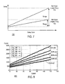
- FIG. 7 is a graph of an embodiment of a generalized delay curve.
- FIG. 8 is a graph of an embodiment of a delay curve over various frequencies.
- Embodiments of the invention provide for a DLL architecture including a coarse-fine type arrangement using one loop for non-continuous strobe that can be also be adapted for continuous clocks as well.
- a reference loop establishes precise coarse unit delay.
- a slave delay line duplicates unit delay.
- a phase interpolator (PI) interpolates between unit delay to produce fine delay.
- Memory transfers data (DQ) at both rising and falling edges of a bi-directional data strobe (DQS) signal.
- DQ data strobe
- a programmable delay locked loop (DLL) is used in a memory controller to generate a precise internal strobe delay allowing the incoming strobe to be placed in the middle of the data eye, to maximize system timing.
- the DLL provides a range of delay with very fine step sizes.
- a phase interpolator takes two successive coarse strobe edge angles and interpolates between them to generate finer strobe edges.
- the memory controller walks through the delay range and selects the optimal delay setting within the passing window.
- Embodiments of the present invention may be implemented in hardware or software, or a combination of both. However, embodiments of the invention may be implemented as computer programs executing on programmable systems comprising at least one processor, a data storage system (including volatile and non-volatile memory and/or storage elements), at least one input device, and at least one output device. Program code may be applied to input data to perform the functions described herein and generate output information. The output information may be applied to one or more output devices, in known fashion.
- a processing system includes any system that has a processor, such as, for example, a digital signal processor (DSP), a micro-controller, an application specific integrated circuit (ASIC), or a microprocessor.
- DSP digital signal processor
- ASIC application specific integrated circuit
- the programs may be implemented in a high level procedural or object oriented programming language to communicate with a processing system.
- the programs may also be implemented in assembly or machine language, if desired.
- the invention is not limited in scope to any particular programming language. In any case, the language may be a compiled or interpreted language.
- the programs may be stored on a storage media or device (e.g., hard disk drive, floppy disk drive, read only memory (ROM), CD-ROM device, flash memory device, digital versatile disk (DVD), or other storage device) readable by a general or special purpose programmable processing system, for configuring and operating the processing system when the storage media or device is read by the processing system to perform the procedures described herein.
- a storage media or device e.g., hard disk drive, floppy disk drive, read only memory (ROM), CD-ROM device, flash memory device, digital versatile disk (DVD), or other storage device
- ROM read only memory
- CD-ROM device compact disc-read only memory
- flash memory device e.g., compact flash memory
- DVD digital versatile disk
- Embodiments of the invention may also be considered to be implemented as a machine-readable storage medium, configured for use with a processing system, where the storage medium so configured causes the processing system to operate in a specific and predefined manner to perform the functions described herein.
- embodiments of the present invention are discussed utilizing a bus, memory controller and memory. Embodiments of the present invention are not limited to such a configuration though.
- FIG. 1 is a diagram illustrating a system in which one embodiment 100 of the invention can be practiced.
- Processor 102 represents a processing unit of any type of architecture such as a microcontroller, a digital signal processor, a state machine, or a central processing unit (CPU).
- the CPU may be implemented with a variety of architecture types such as a complex instruction set computers (CISC), reduced instruction set computers (RISC), very long instruction word (VLIW), or hybrid architecture.
- CISC complex instruction set computers
- RISC reduced instruction set computers
- VLIW very long instruction word
- Processor 102 interfaces with memory controller 104 .
- Memory controller 104 provides memory control functions.
- Memory 106 represents one or more mechanisms for storing information.
- memory 106 may include non-volatile or volatile memories. Examples of these memories include flash memory, read only memory (ROM), or random access memory (RAM).
- Memory 106 may contain a program and other programs and data. Of course, memory 106 preferably contains additional software (not shown), which is not necessary for understanding the invention.
- memory 106 includes double data rate dynamic random access memories (DDR DRAM).
- DDR DRAM uses a double data rate architecture to achieve high-speed operation.
- the double data rate architecture is essentially a 2n-prefetch architecture with an interface designed to transfer two data words per clock cycle at the I/O pins.
- a bi-directional data strobe (DQS) signal is transmitted externally, along with the data (DQ) signal, for use in data capture at the receiver.
- FIG. 2 is a diagram illustrating an embodiment 200 of a DLL architecture according to the invention.
- the architecture includes a master or reference feedback loop 202 , which locks to a reference clock (CLK REF ) 204 that may come from a memory controller, and a slave delay line (coupled with master bias) 206 , phase selection multiplexers 208 and 210 and phase interpolator 212 .
- CLK REF reference clock
- a master-slave arrangement is used since the strobe signal is an asynchronous signal.
- Master loop 202 locks to a reference clock CLK REF (having a period T REF ) 204 .
- delay elements 214 the individual cell delay is T REF /N.
- Feedback loop 218 maintains this cell delay over process, voltage and temperature.
- Master loop 202 generates a set of bias voltages corresponding to operating point.
- PI phase interpolator
- Embodiments of the architecture can be viewed as coarse-fine delay generation architecture.
- the master loop 202 generates and maintains the coarse delay for each delay cell (45 degrees/cell).
- the slave PI interpolates between the coarse delay edges to produce a finer phase step of 6.4 degrees.
- This architecture implements a coarse and fine delay generation scheme using only one feedback loop, as compared to a dual-loop implementation used with continuously running clocks.
- the resolution improvement comes from the use of the phase interpolator, which generates delays that are much lower than the individual cell delay in the previous generation.
- the power improvement comes from lower cell current consumption since the cells are operating at coarse delays instead of fine delays.
- the area reduction is achieved because a few numbers of cells are required to cover the specified delay range.
- asynchronous strobe signal STRB goes through the slave delay line 206 .
- Master delay elements 214 are replicated in the slave delay line 206 , along with bias voltages 216 .
- slave delay line 206 generates a set of (M) equally spaced delayed edges.
- the individual cell delay is controlled by master loop 302 .
- Subsequent edges are selected through multiplexers (odd and even multiplexers) 208 and 210 , and applied to phase/delay interpolator (PI) 212 .
- phase delay/interpolator can generate a set of precise delayed edges, which are selectable through configuration bits.
- Slave delay line 206 includes taps, including the ones at both ends, providing signals that have equally spaced phases. For example, nine taps provides 9 signals that are equally spaced and separated by 45 degrees.
- Slave delay line 206 generates M equally spaced delayed strobe edges.
- Each of the delay elements 214 has an adjustable delay to provide M equally spaced strobe edges.
- Various equally spaced phases are tapped off slave delay line 206 .
- delay line has nine taps, including the ones at both ends, providing nine signals that have equally spaced phases. That is, each of the signals is separated by 45 degrees of phase.
- Two adjacent strobe edges generated are selected and are applied to phase interpolator 212 to generate finer delays within that segment.
- Odd and even multiplexers 208 and 210 are used to connect every other delay element 214 .
- odd numbered delay elements are connected to multiplexer 208 and even numbered delay elements are connected to multiplexer 210 .
- Control signal is applied to each multiplexer 208 and 210 to select adjacent edges that are then applied to phase/delay interpolator 212 .
- phase/delay interpolator 212 For example, adjacent edges 222 and 224 in segment 1 (Seg- 1 ) 220 , corresponding to 45 and 90 degrees, may be selected and applied to phase/delay interpolator 212 for further processing. For the selected segment, phase delay/interpolator 212 can generate a set of precise delayed edges, which are selectable through configuration bits.
- FIG. 3 ( a ) is a diagram of an embodiment 300 of memory 302 , such as DDR DRAM, and memory controller 304 .
- Memory edge aligned data 308 is transferred with a strobe signal 310 .
- the DQS signal is a strobe 310 transmitted by DDR DRAM during a read cycle and by the memory controller, e.g., the memory controller 304 during a write cycle.
- the DQS signal is edge-aligned with the DQ signal 308 for read cycles.
- Memory transfers data (DQ) 308 at both rising and falling edges of a bi-directional data strobe (DQS) signal 310 .
- Embodiments of the present invention are directed to the read cycle where the timing to clock the read data by the DQS signal is critical.
- Memory controller 304 includes a DLL circuit 306 that places the strobe signal or clock at the middle of the data eye, thereby maximizing system timing margin.
- DLL circuit 306 is implemented with a delay line and various equally spaced phases are tapped off of the delay line.
- FIG. 3 ( b ) is diagram of an embodiment 312 of timing signals for DLL circuit 306 shown in FIG. 2 ( a ).
- DLL circuit 306 is used in memory controller 304 to generate an internal strobe delay allowing the incoming strobe 310 to be placed in the middle of data eye (for example, 316 ) to maximizing system timing.
- the protocol for the DQS signal 314 and DQ signal 318 allow a bit value to be asserted simultaneous with each rising or falling edge (for example, 318 and 320 ) of DQS signal 314 .
- the data values D 0 , D 1 , D 2 , and so forth are available starting at alternate rising and falling edges of DQS signal 314 .
- the invention may also be used with a protocol in which only the rising or falling edge, and not both, of the DQS signal 314 are used to mark the associated bit values.
- the DQS signal 310 and DQ signal 308 are received at memory controller 304 following a DQS/DQ flight time interval.
- the received DQS signal 314 is further delayed at the controller 306 , such that its rising or falling edge is positioned closer to the middle of its associated data pulse 308 , for more reliable data capture.
- DLL circuit 306 provides this delay as discussed in detail below.
- DLL circuit 306 provides a range of delays with very fine step sizes. During boot-up, controller walks through the delay range (for example, 1/4Tbit to 3/4Tbit) and selects the best delay setting within the passing window.
- FIG. 4 ( a ) is a diagram of an embodiment 400 of DLL including one master 402 shared with one slave delay line 404 as described above.
- FIG. 4 ( b ) is a detailed diagram of the embodiment 408 shown in FIG. 2 ( a ) including master loop 402 , master delay elements 404 , slave delay line 406 , slave delay elements 408 , multiplexers 410 , 412 , phase interpolator 414 and converter 416 .
- Embodiments of the present invention can be implemented in ACIO loop-back, silicon debug, slew rate control, system margining and so forth.
- _Tbit to _Tbit delay range (Tbit/2 range) with a resolution of ⁇ 25 pS is used.
- the master reference clock frequency scales with DDR MTs, as are individual cell delay, step size and range.
- a programmable master loop element is provided.
- the number of elements to be used is selectable. This allows the range and resolution of the DLL to be changed.
- eight delay elements are used to cover a delay range of Tref (360 degrees). In accordance with embodiments of the invention, more delay elements can be used to cover more range.
- FIG. 5 is a diagram of an embodiment 500 of a DLL implementation.
- Eleven delay elements 504 in the master loop 502 are used to generate edges, which are phased delayed by 32.7 degrees. The tighter phase spacing results in lower noise sensitivity.
- a three-bit thermometer coded phase interpolator 510 generates 4.7 degree fine phase steps to guarantee a monotonic delay.
- a differential implementation may be chosen over single ended.
- DLL can include one master shared with two slave delay lines to support strobes of two different DDR channels.
- FIG. 6 is a flowchart of an embodiment 600 for implanting the invention.
- step 602 a coarse unit delay using a reference feedback circuit is established.
- step 604 the unit delay is duplicated and a plurality of coarsely delayed edges generated, based upon the unit delay in a delay circuit.
- the same delay cells and and bias voltages are used in the delay circuit as the reference feedback circuit. Equally spaced delayed edges are generated in the delay circuit.
- step 606 adjacent edges are selected.
- FIG. 7 is a graph of an embodiment 700 of a generalized delay curve. A delay versus code setting for DDR for lower and higher frequencies is shown.
- Embodiments of the invention provide a delay code that is selectable or software programmable and allows system margining capability. During boot-up, the system will go through a calibration process, walk through all the code settings, and find the best setting for that particular system. Through system margining, the optimum operating point during bootup is determined.
- the DLL provides a range of delay with certain step resolution.
- a higher reference clock frequency 702 provides a “smaller range” with “higher step resolution.”
- a lower reference clock frequency 704 provides “higher range” with “lower step resolution.” This is consistent with a typical usage condition of DLL. For higher frequencies, a higher resolution is desired. Correspondingly, a smaller range is needed. For lower frequencies, a longer delay range is covered. In most cases, a lower resolution is fine since at lower frequencies, there is more margin. Embodiments of the invention provide the capability of system margining. During boot up, the system can walk through the codes and find an optimum operating delay to be used.
- FIG. 8 is a graph of an embodiment 800 of a delay curve over various frequencies.
- the delay curves i.e. typical corner delay versus code settings
- DDR 266, 333 and 400, and DDR2 533 and 667 MTs are shown.
- Tthe delay range and step sizes scale with DDR MTs.
Priority Applications (9)
| Application Number | Priority Date | Filing Date | Title |
|---|---|---|---|
| US10/746,105 US6958634B2 (en) | 2003-12-24 | 2003-12-24 | Programmable direct interpolating delay locked loop |
| TW093139840A TWI266483B (en) | 2003-12-24 | 2004-12-21 | A programmable direct interpolating delay locked loop |
| GB0608722A GB2423204B (en) | 2003-12-24 | 2004-12-22 | A programmable direct interpolating delay locked loop |
| CN2011100593484A CN102195644A (zh) | 2003-12-24 | 2004-12-22 | 可编程序直接插入式延迟锁定环路 |
| DE112004003143T DE112004003143A5 (de) | 2003-12-24 | 2004-12-22 | Programmierbare direkte interpolierende Verzögerungsschleife |
| DE112004002521T DE112004002521T5 (de) | 2003-12-24 | 2004-12-22 | Programmierbare direkte interpolierende Verzögerungsschleife |
| KR1020067012616A KR20060100948A (ko) | 2003-12-24 | 2004-12-22 | 프로그램 가능한 직접 보간 지연 고정 루프 |
| PCT/US2004/043664 WO2005064797A1 (en) | 2003-12-24 | 2004-12-22 | A programmable direct interpolating delay locked loop |
| CNA2004800389048A CN1898871A (zh) | 2003-12-24 | 2004-12-22 | 可编程序直接插入式延迟锁定环路 |
Applications Claiming Priority (1)
| Application Number | Priority Date | Filing Date | Title |
|---|---|---|---|
| US10/746,105 US6958634B2 (en) | 2003-12-24 | 2003-12-24 | Programmable direct interpolating delay locked loop |
Publications (2)
| Publication Number | Publication Date |
|---|---|
| US20050140416A1 US20050140416A1 (en) | 2005-06-30 |
| US6958634B2 true US6958634B2 (en) | 2005-10-25 |
Family
ID=34700613
Family Applications (1)
| Application Number | Title | Priority Date | Filing Date |
|---|---|---|---|
| US10/746,105 Expired - Fee Related US6958634B2 (en) | 2003-12-24 | 2003-12-24 | Programmable direct interpolating delay locked loop |
Country Status (7)
| Country | Link |
|---|---|
| US (1) | US6958634B2 (zh) |
| KR (1) | KR20060100948A (zh) |
| CN (2) | CN102195644A (zh) |
| DE (2) | DE112004003143A5 (zh) |
| GB (1) | GB2423204B (zh) |
| TW (1) | TWI266483B (zh) |
| WO (1) | WO2005064797A1 (zh) |
Cited By (17)
| Publication number | Priority date | Publication date | Assignee | Title |
|---|---|---|---|---|
| US20060022737A1 (en) * | 2004-07-30 | 2006-02-02 | Infineon Technologies Ag | Device for the regulated delay of a clock signal |
| US20060082403A1 (en) * | 2004-10-18 | 2006-04-20 | Kiyoshi Kase | Circuit and method for interpolative delay |
| US20060156101A1 (en) * | 2004-12-28 | 2006-07-13 | Tim Frodsham | Method and system for testing distributed logic circuitry |
| KR100679258B1 (ko) | 2005-04-26 | 2007-02-05 | 삼성전자주식회사 | 지연고정루프회로 및 그에 따른 전송코어클럭신호 발생방법 |
| US20070096787A1 (en) * | 2005-11-03 | 2007-05-03 | United Memories, Inc. | Method for improving the timing resolution of DLL controlled delay lines |
| KR100794999B1 (ko) | 2006-06-07 | 2008-01-16 | 주식회사 하이닉스반도체 | Dll 장치 |
| US7323918B1 (en) * | 2006-08-08 | 2008-01-29 | Micrel, Incorporated | Mutual-interpolating delay-locked loop for high-frequency multiphase clock generation |
| US20080122507A1 (en) * | 2006-11-03 | 2008-05-29 | Yongping Fan | Low power, low phase jitter, and duty cycle error insensitive clock receiver architecture and circuits for source synchronous digital data communication |
| US20080181046A1 (en) * | 2007-01-30 | 2008-07-31 | Atmel Corporation | Clock circuitry for ddr-sdram memory controller |
| US20090039930A1 (en) * | 2007-07-10 | 2009-02-12 | Elpida Memory, Inc | Dll circuit, semiconductor memory device using the same, and data processing system |
| US20100134166A1 (en) * | 2006-10-27 | 2010-06-03 | Jongtae Kwak | System and method for an accuracy-enhanced dll during a measure initialization mode |
| US7872515B1 (en) * | 2009-10-27 | 2011-01-18 | Himax Technologies Limited | Phase interpolation device and slew rate control device thereof |
| US20120182059A1 (en) * | 2005-07-21 | 2012-07-19 | Micron Technology, Inc. | Seamless coarse and fine delay structure for high performance dll |
| US9021154B2 (en) | 2013-09-27 | 2015-04-28 | Intel Corporation | Read training a memory controller |
| US9106230B1 (en) * | 2013-03-14 | 2015-08-11 | Altera Corporation | Input-output circuitry for integrated circuits |
| KR20160114052A (ko) * | 2014-01-30 | 2016-10-04 | 샌디스크 테크놀로지스 엘엘씨 | 지연 동기 루프들에서의 자동 위상 동기화 |
| US20180198439A1 (en) * | 2017-01-11 | 2018-07-12 | Mediatek Inc. | Delay signal generating apparatus using glitch free digitally controlled delay line and associated delay signal generating method |
Families Citing this family (16)
| Publication number | Priority date | Publication date | Assignee | Title |
|---|---|---|---|---|
| DE102004037163B4 (de) * | 2004-07-30 | 2006-08-17 | Infineon Technologies Ag | Vorrichtung zur Einstellung einer Taktverzögerung |
| US7848473B2 (en) * | 2004-12-22 | 2010-12-07 | Agere Systems Inc. | Phase interpolator having a phase jump |
| US7543090B2 (en) * | 2007-01-29 | 2009-06-02 | Via Technologies, Inc. | Double-pumped/quad-pumped variation mechanism for source synchronous strobe lockout |
| KR100825800B1 (ko) * | 2007-02-12 | 2008-04-29 | 삼성전자주식회사 | 딜레이 매트릭스를 구비하는 광대역 다중 위상 출력지연동기 루프 회로 |
| WO2008102246A2 (en) * | 2007-02-22 | 2008-08-28 | Agency For Science, Technology And Research | An apparatus for generating a plurality of signals |
| US7564284B2 (en) * | 2007-03-26 | 2009-07-21 | Infineon Technologies Ag | Time delay circuit and time to digital converter |
| WO2009125508A1 (ja) * | 2008-04-11 | 2009-10-15 | 富士通株式会社 | 位相制御装置、位相制御プリント板および制御方法 |
| US7701246B1 (en) | 2008-07-17 | 2010-04-20 | Actel Corporation | Programmable delay line compensated for process, voltage, and temperature |
| US8102195B2 (en) * | 2009-05-13 | 2012-01-24 | Mediatek Inc. | Digital phase-locked loop circuit including a phase delay quantizer and method of use |
| US8368444B2 (en) | 2010-10-11 | 2013-02-05 | Apple Inc. | Delay locked loop including a mechanism for reducing lock time |
| US8373470B2 (en) | 2010-10-11 | 2013-02-12 | Apple Inc. | Modular programmable delay line blocks for use in a delay locked loop |
| US8593197B1 (en) * | 2012-09-07 | 2013-11-26 | Nanya Technology Corporation | Delay line circuit, delay locked loop and tester system including the same |
| US9137084B2 (en) * | 2013-08-02 | 2015-09-15 | Intel Corporation | Digitally controlled edge interpolator (DCEI) for digital to time converters (DTC) |
| US9652228B2 (en) | 2014-04-03 | 2017-05-16 | Macronix International Co., Ltd. | Devices and operation methods for configuring data strobe signal in memory device |
| CN105629772B (zh) * | 2014-10-30 | 2019-05-07 | 深圳开阳电子股份有限公司 | 一种延时控制装置 |
| US9819479B2 (en) | 2015-09-29 | 2017-11-14 | Intel IP Corporation | Digitally controlled two-points edge interpolator |
Citations (4)
| Publication number | Priority date | Publication date | Assignee | Title |
|---|---|---|---|---|
| US6329859B1 (en) * | 2000-03-23 | 2001-12-11 | Bitblitz Communications, Inc. | N-way circular phase interpolator for generating a signal having arbitrary phase |
| US6525615B1 (en) * | 2000-07-14 | 2003-02-25 | International Business Machines Corporation | Oscillator with digitally variable phase for a phase-locked loop |
| US20030042957A1 (en) | 1997-06-12 | 2003-03-06 | Fujitsu Limited | Timing signal generating circuit, semiconductor integrated circuit device and semiconductor integrated circuit system to which the timing signal generating circuit is applied, and signal transmission system |
| US6650157B2 (en) * | 2002-01-11 | 2003-11-18 | Sun Microsystems, Inc. | Using a push/pull buffer to improve delay locked loop performance |
Family Cites Families (3)
| Publication number | Priority date | Publication date | Assignee | Title |
|---|---|---|---|---|
| JP3955150B2 (ja) * | 1998-01-08 | 2007-08-08 | 富士通株式会社 | 位相インターポレータ、タイミング信号発生回路、および、該タイミング信号発生回路が適用される半導体集積回路装置並びに半導体集積回路システム |
| JP3786540B2 (ja) * | 1999-04-15 | 2006-06-14 | 株式会社ルネサステクノロジ | タイミング制御回路装置 |
| JP3575430B2 (ja) * | 2001-02-01 | 2004-10-13 | 日本電気株式会社 | 2段階可変長遅延回路 |
-
2003
- 2003-12-24 US US10/746,105 patent/US6958634B2/en not_active Expired - Fee Related
-
2004
- 2004-12-21 TW TW093139840A patent/TWI266483B/zh not_active IP Right Cessation
- 2004-12-22 WO PCT/US2004/043664 patent/WO2005064797A1/en active Application Filing
- 2004-12-22 DE DE112004003143T patent/DE112004003143A5/de not_active Withdrawn
- 2004-12-22 CN CN2011100593484A patent/CN102195644A/zh active Pending
- 2004-12-22 GB GB0608722A patent/GB2423204B/en not_active Expired - Fee Related
- 2004-12-22 DE DE112004002521T patent/DE112004002521T5/de not_active Ceased
- 2004-12-22 CN CNA2004800389048A patent/CN1898871A/zh active Pending
- 2004-12-22 KR KR1020067012616A patent/KR20060100948A/ko not_active Application Discontinuation
Patent Citations (4)
| Publication number | Priority date | Publication date | Assignee | Title |
|---|---|---|---|---|
| US20030042957A1 (en) | 1997-06-12 | 2003-03-06 | Fujitsu Limited | Timing signal generating circuit, semiconductor integrated circuit device and semiconductor integrated circuit system to which the timing signal generating circuit is applied, and signal transmission system |
| US6329859B1 (en) * | 2000-03-23 | 2001-12-11 | Bitblitz Communications, Inc. | N-way circular phase interpolator for generating a signal having arbitrary phase |
| US6525615B1 (en) * | 2000-07-14 | 2003-02-25 | International Business Machines Corporation | Oscillator with digitally variable phase for a phase-locked loop |
| US6650157B2 (en) * | 2002-01-11 | 2003-11-18 | Sun Microsystems, Inc. | Using a push/pull buffer to improve delay locked loop performance |
Non-Patent Citations (5)
| Title |
|---|
| "Programmable Memory Controller", IBM Technical Disclosure Bulletin, IBM Corp., New York, USA, vol. 31, No. 9, Feb. 1, 1989, pp. 351-354, XP000097564, ISSN: 0018-8689. |
| EP 1 229 646 A2, Date of Publication Aug. 7, 2002, Inventor: Tanahashi, Toshio, Applicant: NEC Corporation, entitled "Two Step Variable Length Delay Circuit". |
| JP 2000 298532 A (Hitachi Ltd; Hitachi ULSI Systems Co. Ltd.), Oct. 24, 2000. |
| Patent Abstracts of Japan, vol. 1999, No. 14, Dec. 22, 1999 and JP 11 261408, Inventor: Wakayama Shigetoshi, Applicant: Fujitsu Ltd., entitled "Phase Interpolator, Timing Signal Generating Circuit, and Semiconductor Integrated Circuit Device and Semiconductor Integrated Circuit System Adopting the Timing Signal Generating Circuit". |
| PCT International Search Report dated May 6, 2005-related application, International Application No. PCT/US2004/043664-International Filing Date Dec. 22, 2004 (14 pages). |
Cited By (38)
| Publication number | Priority date | Publication date | Assignee | Title |
|---|---|---|---|---|
| US20060022737A1 (en) * | 2004-07-30 | 2006-02-02 | Infineon Technologies Ag | Device for the regulated delay of a clock signal |
| US20060082403A1 (en) * | 2004-10-18 | 2006-04-20 | Kiyoshi Kase | Circuit and method for interpolative delay |
| WO2006044111A3 (en) * | 2004-10-18 | 2006-08-17 | Freescale Semiconductor Inc | Circuit and method for interpolative delay |
| US7116147B2 (en) * | 2004-10-18 | 2006-10-03 | Freescale Semiconductor, Inc. | Circuit and method for interpolative delay |
| US7386773B2 (en) * | 2004-12-28 | 2008-06-10 | Intel Corporation | Method and system for testing distributed logic circuitry |
| US20060156101A1 (en) * | 2004-12-28 | 2006-07-13 | Tim Frodsham | Method and system for testing distributed logic circuitry |
| KR100679258B1 (ko) | 2005-04-26 | 2007-02-05 | 삼성전자주식회사 | 지연고정루프회로 및 그에 따른 전송코어클럭신호 발생방법 |
| US8878586B2 (en) | 2005-07-21 | 2014-11-04 | Micron Technology, Inc. | Seamless coarse and fine delay structure for high performance DLL |
| US8421515B2 (en) * | 2005-07-21 | 2013-04-16 | Micron Technology, Inc. | Seamless coarse and fine delay structure for high performance DLL |
| US20120182059A1 (en) * | 2005-07-21 | 2012-07-19 | Micron Technology, Inc. | Seamless coarse and fine delay structure for high performance dll |
| US20070096787A1 (en) * | 2005-11-03 | 2007-05-03 | United Memories, Inc. | Method for improving the timing resolution of DLL controlled delay lines |
| KR100794999B1 (ko) | 2006-06-07 | 2008-01-16 | 주식회사 하이닉스반도체 | Dll 장치 |
| US7323918B1 (en) * | 2006-08-08 | 2008-01-29 | Micrel, Incorporated | Mutual-interpolating delay-locked loop for high-frequency multiphase clock generation |
| US20080036514A1 (en) * | 2006-08-08 | 2008-02-14 | Micrel, Incorporated | Mutual-interpolating delay-locked loop for high-frequency multiphase clock generation |
| US8928376B2 (en) | 2006-10-27 | 2015-01-06 | Micron Technology, Inc. | System and method for an accuracy-enhanced DLL during a measure initialization mode |
| US8350607B2 (en) | 2006-10-27 | 2013-01-08 | Micron Technology, Inc. | System and method for an accuracy-enhanced DLL during a measure initialization mode |
| US9571105B2 (en) | 2006-10-27 | 2017-02-14 | Micron Technology, Inc. | System and method for an accuracy-enhanced DLL during a measure initialization mode |
| US20100134166A1 (en) * | 2006-10-27 | 2010-06-03 | Jongtae Kwak | System and method for an accuracy-enhanced dll during a measure initialization mode |
| US20080122507A1 (en) * | 2006-11-03 | 2008-05-29 | Yongping Fan | Low power, low phase jitter, and duty cycle error insensitive clock receiver architecture and circuits for source synchronous digital data communication |
| US7501869B2 (en) * | 2006-11-03 | 2009-03-10 | Intel Corporation | Low power, low phase jitter, and duty cycle error insensitive clock receiver architecture and circuits for source synchronous digital data communication |
| US20090010083A1 (en) * | 2007-01-30 | 2009-01-08 | Atmel Corporation | Clock circuitry for ddr-sdram memory controller |
| US7679987B2 (en) | 2007-01-30 | 2010-03-16 | Atmel Corporation | Clock circuitry for DDR-SDRAM memory controller |
| US7423928B2 (en) | 2007-01-30 | 2008-09-09 | Atmel Corporation | Clock circuitry for DDR-SDRAM memory controller |
| US20080181046A1 (en) * | 2007-01-30 | 2008-07-31 | Atmel Corporation | Clock circuitry for ddr-sdram memory controller |
| US7710172B2 (en) * | 2007-07-10 | 2010-05-04 | Elpida Memory, Inc. | DLL circuit, semiconductor memory device using the same, and data processing system |
| US20090039930A1 (en) * | 2007-07-10 | 2009-02-12 | Elpida Memory, Inc | Dll circuit, semiconductor memory device using the same, and data processing system |
| US7872515B1 (en) * | 2009-10-27 | 2011-01-18 | Himax Technologies Limited | Phase interpolation device and slew rate control device thereof |
| US9106230B1 (en) * | 2013-03-14 | 2015-08-11 | Altera Corporation | Input-output circuitry for integrated circuits |
| US9058111B2 (en) | 2013-09-27 | 2015-06-16 | Intel Corporation | Read training a memory controller |
| US9495103B2 (en) | 2013-09-27 | 2016-11-15 | Intel Corporation | Read training a memory controller |
| US9021154B2 (en) | 2013-09-27 | 2015-04-28 | Intel Corporation | Read training a memory controller |
| US9766817B2 (en) | 2013-09-27 | 2017-09-19 | Intel Corporation | Read training a memory controller |
| US10331585B2 (en) | 2013-09-27 | 2019-06-25 | Intel Corporation | Read training a memory controller |
| US10482041B2 (en) | 2013-09-27 | 2019-11-19 | Intel Corporation | Read training a memory controller |
| KR20160114052A (ko) * | 2014-01-30 | 2016-10-04 | 샌디스크 테크놀로지스 엘엘씨 | 지연 동기 루프들에서의 자동 위상 동기화 |
| US20180198439A1 (en) * | 2017-01-11 | 2018-07-12 | Mediatek Inc. | Delay signal generating apparatus using glitch free digitally controlled delay line and associated delay signal generating method |
| US10158352B2 (en) * | 2017-01-11 | 2018-12-18 | Mediatek Inc. | Delay signal generating apparatus using glitch free digitally controlled delay line and associated delay signal generating method |
| TWI659607B (zh) * | 2017-01-11 | 2019-05-11 | 聯發科技股份有限公司 | 延遲信號產生裝置和延遲信號產生方法 |
Also Published As
| Publication number | Publication date |
|---|---|
| GB0608722D0 (en) | 2006-06-14 |
| CN102195644A (zh) | 2011-09-21 |
| WO2005064797A1 (en) | 2005-07-14 |
| TWI266483B (en) | 2006-11-11 |
| DE112004002521T5 (de) | 2006-11-09 |
| GB2423204B (en) | 2007-07-25 |
| CN1898871A (zh) | 2007-01-17 |
| DE112004003143A5 (de) | 2013-07-25 |
| US20050140416A1 (en) | 2005-06-30 |
| TW200535592A (en) | 2005-11-01 |
| KR20060100948A (ko) | 2006-09-21 |
| GB2423204A (en) | 2006-08-16 |
Similar Documents
| Publication | Publication Date | Title |
|---|---|---|
| US6958634B2 (en) | Programmable direct interpolating delay locked loop | |
| US10218342B2 (en) | System and method for duty cycle correction | |
| US6980480B2 (en) | Multi-frequency synchronizing clock signal generator | |
| JP4789172B2 (ja) | 半導体記憶素子におけるディレイロックループ及びそのロック方法 | |
| USRE46231E1 (en) | Duty detection circuit, clock generation circuit including the duty detection circuit, and semiconductor device | |
| US6975149B2 (en) | Method and circuit for adjusting the timing of output data based on an operational mode of output drivers | |
| US6937076B2 (en) | Clock synchronizing apparatus and method using frequency dependent variable delay | |
| US6259288B1 (en) | Semiconductor integrated circuit having a DLL circuit and a special power supply circuit for the DLL circuit | |
| KR100639616B1 (ko) | 반도체 기억 소자에서의 지연 고정 루프 및 그의 록킹 방법 | |
| KR100701423B1 (ko) | 듀티 보정 장치 | |
| US7710171B2 (en) | Delayed locked loop circuit | |
| US7659759B2 (en) | Phase synchronous circuit | |
| US7777542B2 (en) | Delay locked loop | |
| KR102534241B1 (ko) | 위상 감지 회로, 이를 포함하는 클럭 생성 회로 및 반도체 장치 | |
| JPH1139868A (ja) | 半導体集積回路システム、半導体集積回路、及び半導体集積回路システムの駆動方法 | |
| US8073890B2 (en) | Continuous high-frequency event filter | |
| JPH10117142A (ja) | 位相同期ループ回路および半導体集積回路 | |
| JP2005318507A (ja) | 遅延固定ループ回路 | |
| US8081021B2 (en) | Delay locked loop | |
| JP2009021706A (ja) | Dll回路及びこれを用いた半導体記憶装置、並びに、データ処理システム | |
| US20060273834A1 (en) | Delay locked loop and method for setting a delay chain | |
| KR100800139B1 (ko) | 디엘엘 장치 | |
| US5528638A (en) | Multiple phase shifted clocks generation using a minimal set of signals from a PLL | |
| JP2008099002A (ja) | Dll回路 | |
| KR100800138B1 (ko) | 디엘엘 장치 |
Legal Events
| Date | Code | Title | Description |
|---|---|---|---|
| AS | Assignment |
Owner name: INTEL CORPORATION, CALIFORNIA Free format text: ASSIGNMENT OF ASSIGNORS INTEREST;ASSIGNOR:RASHID, MAMUN UR;REEL/FRAME:014853/0654 Effective date: 20031223 |
|
| FPAY | Fee payment |
Year of fee payment: 4 |
|
| FPAY | Fee payment |
Year of fee payment: 8 |
|
| REMI | Maintenance fee reminder mailed | ||
| LAPS | Lapse for failure to pay maintenance fees |
Free format text: PATENT EXPIRED FOR FAILURE TO PAY MAINTENANCE FEES (ORIGINAL EVENT CODE: EXP.) |
|
| STCH | Information on status: patent discontinuation |
Free format text: PATENT EXPIRED DUE TO NONPAYMENT OF MAINTENANCE FEES UNDER 37 CFR 1.362 |
|
| FP | Lapsed due to failure to pay maintenance fee |
Effective date: 20171025 |