US6835696B2 - Method of forming a superconductor film - Google Patents
Method of forming a superconductor film Download PDFInfo
- Publication number
- US6835696B2 US6835696B2 US10/235,788 US23578802A US6835696B2 US 6835696 B2 US6835696 B2 US 6835696B2 US 23578802 A US23578802 A US 23578802A US 6835696 B2 US6835696 B2 US 6835696B2
- Authority
- US
- United States
- Prior art keywords
- film
- substrate
- target
- magnesium
- boron
- Prior art date
- Legal status (The legal status is an assumption and is not a legal conclusion. Google has not performed a legal analysis and makes no representation as to the accuracy of the status listed.)
- Expired - Fee Related, expires
Links
Images


Classifications
-
- H—ELECTRICITY
- H10—SEMICONDUCTOR DEVICES; ELECTRIC SOLID-STATE DEVICES NOT OTHERWISE PROVIDED FOR
- H10N—ELECTRIC SOLID-STATE DEVICES NOT OTHERWISE PROVIDED FOR
- H10N60/00—Superconducting devices
- H10N60/01—Manufacture or treatment
- H10N60/0856—Manufacture or treatment of devices comprising metal borides, e.g. MgB2
-
- C—CHEMISTRY; METALLURGY
- C23—COATING METALLIC MATERIAL; COATING MATERIAL WITH METALLIC MATERIAL; CHEMICAL SURFACE TREATMENT; DIFFUSION TREATMENT OF METALLIC MATERIAL; COATING BY VACUUM EVAPORATION, BY SPUTTERING, BY ION IMPLANTATION OR BY CHEMICAL VAPOUR DEPOSITION, IN GENERAL; INHIBITING CORROSION OF METALLIC MATERIAL OR INCRUSTATION IN GENERAL
- C23C—COATING METALLIC MATERIAL; COATING MATERIAL WITH METALLIC MATERIAL; SURFACE TREATMENT OF METALLIC MATERIAL BY DIFFUSION INTO THE SURFACE, BY CHEMICAL CONVERSION OR SUBSTITUTION; COATING BY VACUUM EVAPORATION, BY SPUTTERING, BY ION IMPLANTATION OR BY CHEMICAL VAPOUR DEPOSITION, IN GENERAL
- C23C14/00—Coating by vacuum evaporation, by sputtering or by ion implantation of the coating forming material
- C23C14/06—Coating by vacuum evaporation, by sputtering or by ion implantation of the coating forming material characterised by the coating material
- C23C14/067—Borides
-
- C—CHEMISTRY; METALLURGY
- C23—COATING METALLIC MATERIAL; COATING MATERIAL WITH METALLIC MATERIAL; CHEMICAL SURFACE TREATMENT; DIFFUSION TREATMENT OF METALLIC MATERIAL; COATING BY VACUUM EVAPORATION, BY SPUTTERING, BY ION IMPLANTATION OR BY CHEMICAL VAPOUR DEPOSITION, IN GENERAL; INHIBITING CORROSION OF METALLIC MATERIAL OR INCRUSTATION IN GENERAL
- C23C—COATING METALLIC MATERIAL; COATING MATERIAL WITH METALLIC MATERIAL; SURFACE TREATMENT OF METALLIC MATERIAL BY DIFFUSION INTO THE SURFACE, BY CHEMICAL CONVERSION OR SUBSTITUTION; COATING BY VACUUM EVAPORATION, BY SPUTTERING, BY ION IMPLANTATION OR BY CHEMICAL VAPOUR DEPOSITION, IN GENERAL
- C23C14/00—Coating by vacuum evaporation, by sputtering or by ion implantation of the coating forming material
- C23C14/22—Coating by vacuum evaporation, by sputtering or by ion implantation of the coating forming material characterised by the process of coating
- C23C14/34—Sputtering
- C23C14/35—Sputtering by application of a magnetic field, e.g. magnetron sputtering
- C23C14/352—Sputtering by application of a magnetic field, e.g. magnetron sputtering using more than one target
-
- C—CHEMISTRY; METALLURGY
- C23—COATING METALLIC MATERIAL; COATING MATERIAL WITH METALLIC MATERIAL; CHEMICAL SURFACE TREATMENT; DIFFUSION TREATMENT OF METALLIC MATERIAL; COATING BY VACUUM EVAPORATION, BY SPUTTERING, BY ION IMPLANTATION OR BY CHEMICAL VAPOUR DEPOSITION, IN GENERAL; INHIBITING CORROSION OF METALLIC MATERIAL OR INCRUSTATION IN GENERAL
- C23C—COATING METALLIC MATERIAL; COATING MATERIAL WITH METALLIC MATERIAL; SURFACE TREATMENT OF METALLIC MATERIAL BY DIFFUSION INTO THE SURFACE, BY CHEMICAL CONVERSION OR SUBSTITUTION; COATING BY VACUUM EVAPORATION, BY SPUTTERING, BY ION IMPLANTATION OR BY CHEMICAL VAPOUR DEPOSITION, IN GENERAL
- C23C14/00—Coating by vacuum evaporation, by sputtering or by ion implantation of the coating forming material
- C23C14/22—Coating by vacuum evaporation, by sputtering or by ion implantation of the coating forming material characterised by the process of coating
- C23C14/56—Apparatus specially adapted for continuous coating; Arrangements for maintaining the vacuum, e.g. vacuum locks
- C23C14/568—Transferring the substrates through a series of coating stations
Definitions
- the present invention relates to a method of forming a superconductor film composed of a compound of magnesium (Mg) and boron (B). More specifically, the ]present invention relates to a method of forming an as-grown film having a high critical temperature superconductor without being annealed.
- a MgB 2 compound features one of the highest transition temperatures of any superconductor. Additionally, a MgB 2 film can be integrated on a substrate to form an integrated circuit. Thus, the MgB 2 compound is expected to apply to electronics devices such as thin film devices.
- the coherent length ⁇ (0) of MgB 2 is 54, and the magnetic penetration depth is 140-180 nm.
- One well known method of making the superconductor of MgB 2 is to form a bulk of MgB 2 by compression molding of powder of mono-crystal MgB 2 , and then annealing the bulk at a high temperature.
- Another method of forming the superconductor of MgB 2 is to form a thin film of a MgB 2 compound by using PLD (pulse laser deposition), and then annealing the thin film of MgB 2 in the temperature range of 600° C.-1200° C. to make the film superconductive.
- PLD pulse laser deposition
- the PLD method focuses a pulsed laser beam on a boron target to evaporate boron atoms and deposit the boron atoms on a substrate.
- the boron atoms on the substrate then react with magnesium atoms in high temperature magnesium vapor to form a MgB 2 film on the substrate. Further, the film is annealed at a high temperature, so as to become a superconductor.
- Another method of forming the superconductor film of a MgB 2 compound by using PLD is that which deposits magnesium and boron atoms on a substrate by laser deposition, and sets the substrate in magnesium vapor.
- the magnesium and boron on the substrate react in the magnesium vapor to form a thin film of the MgB 2 compound on the substrate. Annealing the MgB 2 film at a high temperature enables the film to have the features of a superconductor.
- the present invention features a method of forming a superconductor film of MgB 2 without annealing the as-grown film.
- the present invention provides a method of forming an as-grown film of a superconductor composed of the MgB 2 compound made with magnesium and boron ejected from a magnesium target and a boron target, respectively, in a simultaneous sputtering process.
- the as-grown film composed of the compound of magnesium and boron can be a superconductor without being annealed.
- the as-grown film can be composed of a MgB 2 compound, or the film can be composed of one or more compounds of magnesium and boron different from the MgB 2 compound, or a magnesium element and a boron element in addition to the MgB 2 compound.
- a superconductor film of MgB 2 made using the present invention has features of a superconductor without being annealed, and its critical temperature is in the range of about 6K-29K.
- the present invention can be applied to fabricate an integrated circuit of a superconductor film, because the high temperature annealing process is not needed to make the as-grown film of the MgB 2 compound having features of a superconductor.
- FIG. 1 shows a sputtering apparatus to implement the first embodiment of the present invention.
- FIG. 2 shows an example 1 of resistance-temperature characteristics of a superconductor made by the present invention.
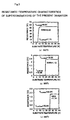
- FIG. 3A shows temperature dependence of resistance-temperature characteristics of a superconductor made by the present invention, where the substrate temperature is 320° C.
- FIG. 3B shows temperature dependence of resistance-temperature characteristics of a superconductor made by the present invention, where the substrate temperature is 350° C.
- FIG. 3C shows temperature dependence of resistance-temperature characteristics of a superconductor made by the present invention, where the substrate temperature is 380° C.
- FIG. 4 shows temperature dependence of critical temperature and residual specific resistance of a superconductor made by the present invention.
- FIG. 5A shows resistance-temperature characteristics of a superconductor of example 2 made by the present invention using the sputtering apparatus shown in FIG. 1 .
- FIG. 5B shows resistance-temperature characteristics of a superconductor of example 2 made by the present invention using the sputtering apparatus shown in FIG. 1, where the axis of abscissas in FIG. 5B is enlarged and corresponds to the region of 0-50 K on the axis of abscissas in FIG. 5 A.
- FIG. 6 shows a static-type sputtering apparatus for implementing the present invention.
- FIG. 1 shows a plan view of an apparatus to implement the present invention, that is a Carrousel-type sputtering apparatus for implementing the present invention.
- the apparatus is composed of a reaction room 1 , pipes 5 and 6 for supplying argon gas, an ion beam source 7 , a buffering room 8 , electric heaters 9 which are lamp heaters for heating substrates 2 , vacuum pumps 10 and 11 , and rotary pumps 12 and 13 .
- Substrates 2 on which the superconductor is formed, are set vertically to the plan view, on a holder.
- the holder is a hexagonal cylinder of six surfaces on which the substrates 2 are arranged.
- the cylinder rotates around an axis.
- the substrates 2 are, for example, Al 2 O 3 , MgO, SiO 2 , etc.
- a magnesium target 3 of purity of 99.9%, a boron target 4 of purity of 99.5%, an aluminum target 15 , and a niobium target 16 ′ are set vertically to the plan view on the wall of the reaction room 1 . Each target is faced to one of the substrates 2 .
- the aluminum target 15 and the niobium target 16 ′ are not used for forming a MgB 2 film.
- the ion beam source 7 generates argon ions and the ions are irradiated to the substrates 2 to clean their surfaces.
- the reaction room 1 is exhausted to vacuum by the vacuum pumps 10 and 11 and the rotary pumps 12 and 13 . Further, argon gas fills in the reaction room 1 .
- High voltage is applied between the magnesium target 3 and the substrate 2 , and between the boron target 4 and the substrate 2 .
- DC voltage is applied between the magnesium target 3 and the substrate 2 so that the magnesium target 3 is positive voltage.
- AC voltage is applied between the boron target 4 and the substrate 2 .
- the argon gas is discharged between the target and the substrate of each target and substrate pair. The gas discharges can be run simultaneously at each target and substrate pair, and each of the discharges can be controlled independently. During the discharge, the substrates 2 are heated by the electric heaters 9 .
- the discharge between the magnesium target 3 and the substrate 2 is DC discharge, applying positive DC voltage to the magnesium target 3 .
- the discharge between the boron target 4 and the substrate 2 is high frequency discharge, thus applying high frequency alternating voltage between the boron target 4 and the substrate 2 .
- the argon gas is discharged between the magnesium target 3 and the substrate 2 , and between the boron target 4 and the substrate 2 .
- the argon ions generated during the discharge result in ion bombardments to the magnesium target 3 and the boron target 4 .
- atoms or ions of magnesium and atoms or ions of boron are ejected from each target, respectively, when the argon atoms or ions impact the targets.
- the magnesium atoms or ions and the boron atoms or ions react with each other in the reaction room 1 to produce compounds of magnesium and boron.
- the compound of magnesium and boron is then deposited on the substrates 2 , which rotate in a plane vertical to the plan view around an axis with high speed.
- the magnesium atoms or ions and the boron atoms or ions are deposited on the substrates 2 , and they react on the substrates 2 to produce the compound of magnesium and boron.
- the sputtering process in simultaneous ion bombardments to the magnesium target and the boron target is called simultaneous magnesium and boron sputtering.
- the as-grown film formed by the above mentioned method is usually polycrystalline, which is composed of only MgB 2 , or composed of the MgB 2 compound and one or more than one of a magnesium element, a boron element, or compounds of magnesium and boron different from MgB 2 .
- the film made by the present invention is usually composed of the components mentioned above. However, for the purpose of clarity, the present invention will be explained by a film composed of only a MgB 2 compound.
- the substrates which are used in this embodiment of the present invention are Al 2 O 3 , MgO, or SiO 2 .
- the temperature of each substrate is in the range of 250° C.-400° C. in the as-grown film forming process.
- the purity of argon gas is 99.9999%.
- the reaction pressure is in the range of 2-5 mTorr.
- the rotation speed of the substrates is 50 rpm.
- the input power for the discharge between the boron target and the substrate is high frequency AC power of 800 W.
- the input power for the discharge between the magnesium target and the substrate is DC power of 300 W.
- the reaction time to form the film is 10-60 minutes.
- FIG. 2 shows resistance-temperature characteristics of the MgB 2 film made by the simultaneous magnesium and boron spattering using the Carrousel-type sputtering apparatus shown in FIG. 1 .
- the substrate of the experiment is Al 2 O 3 ( 1102 ).
- the film forming conditions are the substrate temperature being 380° C., the input power for discharging the gas between the boron target and the substrate being AC power of 800W, the input power of the discharge between the magnesium target and the substrate being DC power of 300W, and the reaction pressure being 5 mTorr (argon gas pressure).
- the reaction pressure being 5 mTorr (argon gas pressure).
- the resistance-temperature characteristics are shown in FIG. 2 .
- the critical temperature Tc is about 28 K, which shows that the film is superconductive at a high temperature.
- FIGS. 3A, 3 B, and 3 C show the temperature dependence of the resistance-temperature characteristics.
- the resistance-temperature characteristics are measured at various temperatures as a parameter.
- FIGS. 3A, 3 B, and 3 C show the resistance-temperature characteristics at the substrate temperatures of 320° C., 350° C., and 380° C., respectively, without annealing the as-grown film.
- the films are formed during the simultaneous magnesium and boron sputtering by the Carrousel-type sputtering apparatus.
- the substrate ( 1102 ) is Al 2 O 3 .
- the input power for the discharge between the boron target and the substrate is AC power of 800W, and the input power for the discharge between the magnesium target and the substrate is DC power of 300W.
- the reaction pressure is 2 mTorr (in argon gas).
- the as-grown films formed by the simultaneous magnesium and boron sputtering in the apparatus shown in FIG. 1 have features of a superconductor without being annealed.
- the RRR Residual Resistance Ratio
- the RRR is the resistance ratio at 300K and 40K, and shows the degree of film fineness as a superconductor. It is known that the greater the RRR of the film is, the less the specific resistance of the film is, and the nearer to metal the film is.
- FIG. 3A shows a case in which the substrate temperature is 320° C.
- FIG. 3B shows a film formed on a substrate with a temperature of 350. This figure shows that an as-grown film of MgB 2 of critical temperature Tc 19K and RRR 1.10 can be formed without being annealed.
- FIG. 4 shows the dependence of critical temperature and residual resistance ratio of the film formed by the present invention on substrate temperature. Relations of the critical temperature and the residual resistance ratio to the substrate temperature are measured at various substrate temperatures to form the as-grown film of MgB 2 .
- FIG. 4 shows the results.
- the condition to form the film is the same as the conditions set forth for FIGS. 3A, 3 B and 3 C.
- the circled black dots show the relationship between substrate temperature and critical temperature
- the uncircled black dots show the relationship between residual resistance ratio and the substrate temperature.
- the critical temperature and the residual resistance ratio corresponding to the same substrate temperature are those of the MgB 2 film on the substrate.
- the values of residual resistance ratio at 300° C. are higher than the values at another substrate temperature. This is believed to occur because of the high magnesium rate near the substrate.
- the high temperature superconductor feature of residual resistance ratio is 1.0-1.7.
- the as-grown film of MgB 2 formed on the rotating substrate facing to the magnesium target and the boron target in the simultaneous sputtering process has features of a high critical temperature superconductor without annealing the as-grown film.
- the substrates are rotated with high speed, however, it has been found by the inventors of the present invention that an as-grown film of MgB 2 formed by the simultaneous sputtering process on a substrate kept static has features of a superconductor at a high temperature without annealing the as-grown film, similar to those of films formed on the rotating substrate with high speed in the simultaneous sputtering process.
- FIGS. 5A and 5B show resistance-temperature characteristics of MgB 2 film which is made by a second embodiment of the present invention method.
- the axis of abscissas in FIG. 5B is enlarged and corresponds to the region of 0-50 on the axis of abscissas in FIG. 5 A.
- the as-grown film of MgB 2 made by method of the second embodiment of the present invention is formed on an immovable substrate, which is different from the method of embodiment 1 which uses rotating substrates.
- the resistance-temperature characteristics in FIGS. 5A and 5B are those of MgB 2 film formed on an immobile substrate 2 , using the Carrousel-type simultaneous sputtering apparatus shown in FIG. 1 .
- a substrate 2 is located so as to face to the middle between the magnesium target 3 and boron target 4 in the Carrousel-type sputtering apparatus, and is fixed at the position.
- the substrate on which the MgB 2 film is formed is Al 2 O 3 ( 1102 ).
- the conditions for forming an as-grown film of MgB 2 are a substrate temperature of 340° C. in the film forming process, the application of AC power of 800 W for the discharge between the magnesium target and the substrate, the application of DC power of 300 W for the discharge between the magnesium and the substrate, the reaction pressure of 5.0 mTorr in argon gas, and a reaction time of 20 minutes for forming the film.
- the as-grown film of MgB 2 formed by the second embodiment of the present invention has features of the superconductor without annealing the as-grown film.
- FIGS. 5A and 5B show that a film fabricated on the immobile substrate by simultaneous magnesium and boron sputtering has features of a superconductor.
- the film is fabricated by using Carrousel-type simultaneous sputtering apparatus in a mode in which its substrate holder is not rotated.
- the MgB 2 film of the present invention can be formed with a static-type simultaneous sputtering apparatus.
- FIG. 6 shows an outline of the static-type simultaneous sputtering apparatus.
- the static-type spattering apparatus is composed of a reaction room 1 , pipes 5 and 6 for supplying argon gas, ion beam source 7 , buffering room 8 , electric heaters 9 which are lamp heaters for heating substrates 2 , vacuum pumps 10 and 11 , rotary pumps 12 and 13 , a substrate transportation rod 14 , an axis of substrate holder 15 ′ which rotates the substrate 2 in a horizontal plane, a shutter 16 , 17 which controls a film thickness, blocking the flow of ejected magnesium or boron atoms or ions, and a heater 17 ′ which heats the substrate 2 .
- Argon gas enters the reaction room 1 .
- Positive DC voltage is applied between the substrate 2 and the magnesium target 3 .
- High frequency AC voltage is applied between the boron target 4 and the substrate 2 .
- Argon gas is then discharged between the magnesium target 3 and the substrate 2 and between the boron target 4 and the substrate 2 , as a result of the applied voltage.
- the discharge between the substrate 2 and the magnesium target 3 , and the discharge between the substrate 2 and the boron target 4 can be controlled independently in the simultaneous magnesium and boron sputtering process.
- the argon ions bombard the magnesium target 3 and the boron target 4 to eject magnesium atoms and boron atoms, respectively, from each target.
- the atoms or ions of the magnesium and boron react to each other in the reaction room 1 to produce molecules of a MgB 2 compound.
- the MgB 2 molecules and an as-grown film of MgB 2 are then deposited on the substrate.
- the atoms or ions of the magnesium or the boron ejected from each target, respectively are deposited on the substrate and the magnesium element and the boron element and react to produce an as-grown film of MgB 2 .
- the as-grown film has features of a superconductor without being annealed.
- MgB 2 film formed by the method explained above is usually polycrystalline.
- a mono-crystalline or amorphous film of MgB 2 which is formed by the simultaneous magnesium and boron sputtering process has features of a superconductor without being annealed. Such films are involved in the scope of the present invention.
Landscapes
- Chemical & Material Sciences (AREA)
- Engineering & Computer Science (AREA)
- Chemical Kinetics & Catalysis (AREA)
- Materials Engineering (AREA)
- Mechanical Engineering (AREA)
- Metallurgy (AREA)
- Organic Chemistry (AREA)
- Manufacturing & Machinery (AREA)
- Physical Vapour Deposition (AREA)
- Inorganic Compounds Of Heavy Metals (AREA)
- Superconductor Devices And Manufacturing Methods Thereof (AREA)
- Superconductors And Manufacturing Methods Therefor (AREA)
Applications Claiming Priority (2)
| Application Number | Priority Date | Filing Date | Title |
|---|---|---|---|
| JP2001-356802 | 2001-11-22 | ||
| JP2001356802A JP4296256B2 (ja) | 2001-11-22 | 2001-11-22 | 超伝導材料の製造方法 |
Publications (2)
| Publication Number | Publication Date |
|---|---|
| US20030096711A1 US20030096711A1 (en) | 2003-05-22 |
| US6835696B2 true US6835696B2 (en) | 2004-12-28 |
Family
ID=19168256
Family Applications (1)
| Application Number | Title | Priority Date | Filing Date |
|---|---|---|---|
| US10/235,788 Expired - Fee Related US6835696B2 (en) | 2001-11-22 | 2002-09-06 | Method of forming a superconductor film |
Country Status (2)
| Country | Link |
|---|---|
| US (1) | US6835696B2 (ja) |
| JP (1) | JP4296256B2 (ja) |
Cited By (7)
| Publication number | Priority date | Publication date | Assignee | Title |
|---|---|---|---|---|
| US20050116204A1 (en) * | 2003-12-01 | 2005-06-02 | Superconductor Technologies, Inc. | Growth of in-situ thin films by reactive evaporation |
| US20090258787A1 (en) * | 2008-03-30 | 2009-10-15 | Hills, Inc. | Superconducting Wires and Cables and Methods for Producing Superconducting Wires and Cables |
| US7881208B1 (en) | 2001-06-18 | 2011-02-01 | Cisco Technology, Inc. | Gateway load balancing protocol |
| US7966409B1 (en) | 2000-01-18 | 2011-06-21 | Cisco Technology, Inc. | Routing protocol based redundancy design for shared-access networks |
| US8077604B1 (en) | 1999-06-29 | 2011-12-13 | Cisco Technology, Inc. | Load sharing and redundancy scheme |
| USRE44661E1 (en) | 2000-01-18 | 2013-12-24 | Cisco Technology, Inc. | Method for a cable modem to rapidly switch to a backup CMTS |
| US9136457B2 (en) | 2006-09-20 | 2015-09-15 | Hypres, Inc. | Double-masking technique for increasing fabrication yield in superconducting electronics |
Families Citing this family (11)
| Publication number | Priority date | Publication date | Assignee | Title |
|---|---|---|---|---|
| DE10341914B4 (de) * | 2003-09-11 | 2008-08-14 | Forschungszentrum Karlsruhe Gmbh | Einrichtung zur Herstellung dünner Schichten und Verfahren zum Betreiben der Einrichtung |
| US7226894B2 (en) | 2003-10-22 | 2007-06-05 | General Electric Company | Superconducting wire, method of manufacture thereof and the articles derived therefrom |
| JP4491262B2 (ja) * | 2004-03-19 | 2010-06-30 | 株式会社シンクロン | スパッタ装置及び薄膜形成方法 |
| JP4811552B2 (ja) * | 2004-03-30 | 2011-11-09 | 独立行政法人科学技術振興機構 | 超伝導素子を用いた中性子検出装置 |
| JP4922756B2 (ja) * | 2004-04-09 | 2012-04-25 | 株式会社アルバック | 成膜装置および成膜方法 |
| DE102004046280A1 (de) * | 2004-09-23 | 2006-04-13 | Forschungszentrum Karlsruhe Gmbh | Drehbarer Substrathalter |
| JP2006237384A (ja) * | 2005-02-25 | 2006-09-07 | National Institute Of Information & Communication Technology | 積層型全MgB2SIS接合および積層型全MgB2SIS接合方法 |
| US7985713B2 (en) | 2005-03-25 | 2011-07-26 | Incorporated National University Iwate University | Superconducting magnesium boride thin-film and process for producing the same |
| JP5041734B2 (ja) * | 2006-05-24 | 2012-10-03 | 株式会社日立製作所 | 二ホウ化マグネシウム超電導薄膜の作製方法および二ホウ化マグネシウム超電導薄膜 |
| CN103469157B (zh) * | 2013-09-18 | 2015-05-27 | 大连理工常州研究院有限公司 | 一种非晶基B-C-Mg三元薄膜及其制备方法 |
| CN106011765A (zh) * | 2016-07-12 | 2016-10-12 | 广东振华科技股份有限公司 | 一种磁控溅射真空镀膜设备 |
Citations (2)
| Publication number | Priority date | Publication date | Assignee | Title |
|---|---|---|---|---|
| US4629547A (en) * | 1983-11-16 | 1986-12-16 | Hitachi, Ltd. | Process for forming protective film of organic polymer and boron |
| US6626995B2 (en) * | 2001-06-01 | 2003-09-30 | Electronics And Telecommunications Research Institute | Superconductor incorporating therein superconductivity epitaxial thin film and manufacturing method thereof |
-
2001
- 2001-11-22 JP JP2001356802A patent/JP4296256B2/ja not_active Expired - Lifetime
-
2002
- 2002-09-06 US US10/235,788 patent/US6835696B2/en not_active Expired - Fee Related
Patent Citations (2)
| Publication number | Priority date | Publication date | Assignee | Title |
|---|---|---|---|---|
| US4629547A (en) * | 1983-11-16 | 1986-12-16 | Hitachi, Ltd. | Process for forming protective film of organic polymer and boron |
| US6626995B2 (en) * | 2001-06-01 | 2003-09-30 | Electronics And Telecommunications Research Institute | Superconductor incorporating therein superconductivity epitaxial thin film and manufacturing method thereof |
Non-Patent Citations (10)
| Title |
|---|
| Atsushi Saito, et al., "As-Grown Deposition of MgB2 Thin Film and Fabrication of Josephson Junctions", The Institute of Electronics, Information and Communication Engineers, Technical Report of IEICE.SCE2002-2, MW2002-2 (200-04). |
| Atsushi Saito, et al., "As-Grown Deposition of Superconducting MgB2 Thin Films by Multiple-Target Sputtering System", (1) Jpn.J.Appl.Phys.vol. 41 (2002)pp. L127-129 Part 2, No. 2A, Feb. 1, 2002, |
| Atsushi Saito, et al., "As-Grown MgB2 Thin Film Deposited On Al2O3 Substrates With Different Crystal Plane," Super Conductor Science and Technology 15 (2002) 1-5, Received Jun. 24, 2002. |
| Atsushi Saito, et al., "As-Grown MgB2 Thin Films Deposited On Al2O3 Substrates With Different Crystal Plane," International Conference on Electronics Materials, Jun. 12, 2002, Abstract. |
| Atsushi Saito, et al., "Fabrication of Josephson Junctions As-Grown MgB2 Thin Films," Applied Superconductivity Conference Aug. 8, 2002 Abstract (4EG11). |
| Atsushi Saito, et al., "Fabrication of Josephson Junctions As-Grown MgB2 Thin Films," The Japan Society of Applied Physics, No. 49, Mar., 2002, Abstract 28a-ZB-3. |
| Atsushi Saito, et al., "Low Temperature Fabrication of As-Grown MgB2 Thin Films by Carrousel-Type Sputtering Apparatus", The Japan Society of Applied Physic, No. 62, Sep. 12, 2002, Abstract 12p-M-9. |
| Dave H. Blank, et al., "Superconducting Mg-B Films by Pulsed-Laser Deposition in an In Situ Two-Step Process Using Multicomponent Targets," Applied Physics Letters, vol. 79, No. 3, Jul. 16, 2001, pp 394-396. |
| Jun Nagamatsu, et al., "Superconductivity at 39K in Magnesium Diboride," Nature, vol. 410, p63-64, Mar. 2001. |
| S.R. Shinde, et al., "Superconducting MgB2 Thin Films by Pulsed Laser Deposition," Applied Physics Letters, vol. 79, No. 2, Jul. 9, 2001, pp 227-229. |
Cited By (14)
| Publication number | Priority date | Publication date | Assignee | Title |
|---|---|---|---|---|
| US9276834B2 (en) | 1999-06-29 | 2016-03-01 | Cisco Technology, Inc. | Load sharing and redundancy scheme |
| US8077604B1 (en) | 1999-06-29 | 2011-12-13 | Cisco Technology, Inc. | Load sharing and redundancy scheme |
| US7966409B1 (en) | 2000-01-18 | 2011-06-21 | Cisco Technology, Inc. | Routing protocol based redundancy design for shared-access networks |
| USRE44661E1 (en) | 2000-01-18 | 2013-12-24 | Cisco Technology, Inc. | Method for a cable modem to rapidly switch to a backup CMTS |
| US7881208B1 (en) | 2001-06-18 | 2011-02-01 | Cisco Technology, Inc. | Gateway load balancing protocol |
| US8022012B2 (en) | 2003-12-01 | 2011-09-20 | Superconductor Technologies, Inc. | Device and method for fabricating thin films by reactive evaporation |
| US20050116204A1 (en) * | 2003-12-01 | 2005-06-02 | Superconductor Technologies, Inc. | Growth of in-situ thin films by reactive evaporation |
| US8290553B2 (en) | 2003-12-01 | 2012-10-16 | Superconductor Technologies, Inc. | Device and method for fabricating thin films by reactive evaporation |
| US20090068355A1 (en) * | 2003-12-01 | 2009-03-12 | Superconductor Technologies, Inc. | Device and method for fabricating thin films by reactive evaporation |
| US7439208B2 (en) * | 2003-12-01 | 2008-10-21 | Superconductor Technologies, Inc. | Growth of in-situ thin films by reactive evaporation |
| US9136457B2 (en) | 2006-09-20 | 2015-09-15 | Hypres, Inc. | Double-masking technique for increasing fabrication yield in superconducting electronics |
| US9595656B2 (en) | 2006-09-20 | 2017-03-14 | Hypres, Inc. | Double-masking technique for increasing fabrication yield in superconducting electronics |
| US10109673B2 (en) | 2006-09-20 | 2018-10-23 | Hypres, Inc. | Double-masking technique for increasing fabrication yield in superconducting electronics |
| US20090258787A1 (en) * | 2008-03-30 | 2009-10-15 | Hills, Inc. | Superconducting Wires and Cables and Methods for Producing Superconducting Wires and Cables |
Also Published As
| Publication number | Publication date |
|---|---|
| JP4296256B2 (ja) | 2009-07-15 |
| US20030096711A1 (en) | 2003-05-22 |
| JP2003158307A (ja) | 2003-05-30 |
Similar Documents
| Publication | Publication Date | Title |
|---|---|---|
| US6835696B2 (en) | Method of forming a superconductor film | |
| Cho et al. | Background oxygen effects on pulsed laser deposited Na 0.5 K 0.5 NbO 3 films: From superparaelectric state to ferroelectricity | |
| CN113789503B (zh) | 一种具有抗氧化特性的高熵硅化物薄膜的原位合成方法 | |
| Ma et al. | A study of preferred orientation of vanadium nitride and zirconium nitride coatings on silicon prepared by ion beam assisted deposition | |
| Rost et al. | Deposition and analysis of lithium niobate and other lithium niobium oxides by rf magnetron sputtering | |
| Willey | Practical production of optical thin films | |
| Wu et al. | Tailoring of titanium thin film properties in high power pulsed magnetron sputtering | |
| Bleykher et al. | Magnetron deposition of coatings with evaporation of the target | |
| Sidelev et al. | Aluminum films deposition by magnetron sputtering systems: Influence of target state and pulsing unit | |
| KR100732498B1 (ko) | 스퍼터 증착의 실버 셀레나이드 막 화학양론 및 형상 제어 | |
| US6929820B2 (en) | Method of forming a superconductor film | |
| Nazabal et al. | Amorphous thin film deposition | |
| Asgary et al. | Evolution of Structural, Morphological, Mechanical and Optical properties of TiAlN coatings by Variation of N and Al amount | |
| US7799180B2 (en) | Silver selenide sputtered films and method and apparatus for controlling defect formation in silver selenide sputtered films | |
| Safi | A novel reactive magnetron sputtering technique for producing insulating oxides of metal alloys and other compound thin films | |
| JP2001073131A (ja) | 銅薄膜製造方法、及びその方法に用いるスパッタ装置 | |
| Hashizume et al. | Fabrication of Tantalum nitride thin film using the low vacuum magnetron sputtering system | |
| JP3787430B2 (ja) | スパッタリング装置及びそれを用いた薄膜形成法 | |
| Kang et al. | Crystallization of lithium cobalt oxide thin films by radio-frequency plasma irradiation | |
| Li et al. | The influence of columnar microstructure on diffusion reaction between Ti thin films and aluminum nitride ceramics | |
| Lin et al. | Low-temperature fabrication of VO2 thin film on ITO glass with a Mott transition | |
| Tunaboylu et al. | Phase transformation and paired-plate precipitate formation in Pb0. 91La0. 09Zr0. 65Ti0. 35O3 films grown on sapphire substrates | |
| Nowakowska-Langier | Development of plasma and ion beam technology for material engineering at NCBJ | |
| Rastogi et al. | The effect of oxygen impurity on growth of molybdenum disilicide and its distribution during rapid thermal annealing of co-sputtered MoSix thin films | |
| Turenko et al. | Plasma synthesis of thin copper silicide films on single-crystal silicon |
Legal Events
| Date | Code | Title | Description |
|---|---|---|---|
| AS | Assignment |
Owner name: COMMUNICATIONS RESEARCH LABORATORY, JAPAN Free format text: ASSIGNMENT OF ASSIGNORS INTEREST;ASSIGNORS:SAITO, ATSUSHI;KAWAKAMI, AKIRA;SHIMAKAGE, HISASHI;AND OTHERS;REEL/FRAME:013278/0390 Effective date: 20020819 |
|
| AS | Assignment |
Owner name: NATIONAL INSTITUTE OF INFORMATION AND COMMUNICATIO Free format text: ASSIGNMENT OF ASSIGNORS INTEREST;ASSIGNOR:COMMUNICATIONS RESEARCH LABORATORY INDEPENDENT ADMINISTRATIVE INSTITUTION;REEL/FRAME:015851/0991 Effective date: 20040401 |
|
| CC | Certificate of correction | ||
| FPAY | Fee payment |
Year of fee payment: 4 |
|
| REMI | Maintenance fee reminder mailed | ||
| LAPS | Lapse for failure to pay maintenance fees | ||
| STCH | Information on status: patent discontinuation |
Free format text: PATENT EXPIRED DUE TO NONPAYMENT OF MAINTENANCE FEES UNDER 37 CFR 1.362 |
|
| FP | Lapsed due to failure to pay maintenance fee |
Effective date: 20121228 |