US6835636B2 - Method for fabricating source/drain devices - Google Patents
Method for fabricating source/drain devices Download PDFInfo
- Publication number
- US6835636B2 US6835636B2 US10/315,980 US31598002A US6835636B2 US 6835636 B2 US6835636 B2 US 6835636B2 US 31598002 A US31598002 A US 31598002A US 6835636 B2 US6835636 B2 US 6835636B2
- Authority
- US
- United States
- Prior art keywords
- gate
- area
- photo resist
- semiconductor substrate
- resist layer
- Prior art date
- Legal status (The legal status is an assumption and is not a legal conclusion. Google has not performed a legal analysis and makes no representation as to the accuracy of the status listed.)
- Expired - Lifetime, expires
Links
Images


Classifications
-
- H—ELECTRICITY
- H10—SEMICONDUCTOR DEVICES; ELECTRIC SOLID-STATE DEVICES NOT OTHERWISE PROVIDED FOR
- H10D—INORGANIC ELECTRIC SEMICONDUCTOR DEVICES
- H10D30/00—Field-effect transistors [FET]
- H10D30/01—Manufacture or treatment
- H10D30/021—Manufacture or treatment of FETs having insulated gates [IGFET]
- H10D30/0221—Manufacture or treatment of FETs having insulated gates [IGFET] having asymmetry in the channel direction, e.g. lateral high-voltage MISFETs having drain offset region or extended-drain MOSFETs [EDMOS]
-
- H—ELECTRICITY
- H10—SEMICONDUCTOR DEVICES; ELECTRIC SOLID-STATE DEVICES NOT OTHERWISE PROVIDED FOR
- H10D—INORGANIC ELECTRIC SEMICONDUCTOR DEVICES
- H10D30/00—Field-effect transistors [FET]
- H10D30/60—Insulated-gate field-effect transistors [IGFET]
- H10D30/601—Insulated-gate field-effect transistors [IGFET] having lightly-doped drain or source extensions, e.g. LDD IGFETs or DDD IGFETs
- H10D30/603—Insulated-gate field-effect transistors [IGFET] having lightly-doped drain or source extensions, e.g. LDD IGFETs or DDD IGFETs having asymmetry in the channel direction, e.g. lateral high-voltage MISFETs having drain offset region or extended drain IGFETs [EDMOS]
Definitions
- the invention relates to a semiconductor process, and more particularly to a source/drain (S/D) device fabrication process used in a high voltage circuit element.
- S/D source/drain
- FIGS. 1 a to 1 i are cross-sections of the conventional method for fabricating S/D device.
- a semiconductor substrate 101 such as silicon, is provided, and a first isolation area 105 a and a second isolation area 105 b are formed thereon.
- a pad layer 102 such as oxide, a conductive layer 103 , such as poly, and a first patterned photo resist layer 104 are sequentially formed in the area between the first isolation area 105 a and the second isolation area 105 b .
- the area surrounding the isolation area areas is an active area (AA).
- the first patterned photo resist layer 104 is removed. Then, the area of the semiconductor substrate 101 between the gate 103 a and the first isolation area 105 a is doped to form a lightly doped area 106 .
- an isolating layer 107 such as nitride, is conformably formed on the surface of the pad layer 102 and the gate 103 a.
- the isolating layer 107 is isotropically etched to form a spacer 107 a on the sidewall of the gate 103 a.
- a second patterned photo resist layer 108 having a first opening 109 a and a second opening 109 b is formed on the semiconductor substrate 101 .
- the first opening 109 a is positioned in the area between the gate 103 a and the first isolation area 105 a
- the second opening 109 b is positioned in the area between the gate 103 a and the second isolation area 105 b.
- First ion implantation is performed on the semiconductor substrate 101 using the second patterned photo resist layer 108 as a mask with As or B ions.
- FIG. 2 is a top view of FIG. 1 e .
- part of the active area and half the width of the gate 103 a are exposed by the first opening 109 a in the second patterned photo resist layer 108 .
- a first doped area 110 a is formed at the bottom of the first opening 109 a and a second doped area 110 b is formed at the bottom of the second opening 109 b .
- the second patterned photo resist layer 108 is removed.
- a third patterned photo resist layer 111 having a third opening 112 is formed on the semiconductor substrate 101 , and half the width of the gate 103 a is exposed by the third opening 112 in the third patterned photo resist layer 111 .
- the third opening 112 is positioned in the area between the gate 103 a and the second isolation area 105 b.
- Second ion implantation is performed on the semiconductor substrate 101 using the third patterned photo resist layer 111 as a mask and the semiconductor substrate 101 is annealed with As or B ions.
- FIG. 3 is a top view of FIG. 1 f .
- part of the active area and half the width of the gate 103 a are exposed by the first opening 112 in the third patterned photo resist layer 111 , and the area between the gate 103 a and the first isolating 105 a is covered with the third patterned photo resist layer 111 .
- a deeply doped area 113 is formed at the bottom of the third opening 112 .
- the third patterned photo resist layer 111 is removed.
- the deeply doped area 113 is 6-7 times the depth of the first doped area 11 a and the second doped area 110 b .
- the deeply doped area 113 expands after annealing, such that the depth and the width of the deeply doped area 113 are both increased.
- the concentration of dopant inside the deeply doped area 113 decreases and the breakdown voltage of the deeply doped area 113 increases accordingly.
- implantation depth into the substrate can be controlled. Meanwhile, the ions also penetrate the gate 103 a and the spacer 107 a into the semiconductor substrate 101 , and the size increases after annealing.
- the channel between the S/D consisting of the first doped area 110 a and another S/D consisting of the second doped area 110 b and deeply doped area 113 is decreased, resulting in Short Channel Effect.
- the channel between the S/D devices below the gate 103 a and spacer 107 a punches through, such that electrons are injected into the channel from source region before applying a gate voltage.
- the present invention is directed to a method for fabricating source/drain devices in a high voltage circuit element without additional process.
- the present invention provides a method for fabricating a source/drain device, in which, first, a semiconductor substrate having a gate is provided. A hard mask layer is formed on the gate. A first doped area is positioned on a first side of the gate on the semiconductor substrate, and a second doped area is positioned on a second side of the gate on the semiconductor substrate and spaced between. A patterned photo resist layer having an opening on the second side of the gate is formed on the semiconductor substrate, and the exposed gate is equal to half the width of the gate. The semiconductor substrate is implanted and annealed to form a dual diffusion area on the second side of the gate using the patterned photo resist layer and the hard mask layer as masks.
- the present invention also provides a method for fabricating source/drain devices.
- a silicon substrate having a gate is provided.
- a hard mask layer is formed on the gate.
- a first doped area is positioned on a first side of the gate on the silicon substrate, and a second doped area is positioned on a second side of the gate on the silicon substrate and spaced between.
- a patterned photo resist layer having an opening on the second side of the gate is formed on the semiconductor substrate, and the width of the exposed gate is equal to half the width of the gate.
- the silicon substrate is implanted and annealed to form a dual diffusion area on the second side of the gate using the patterned photo resist layer and the hard mask layer as masks.
- the present invention also provides a method for fabricating a source/drain device.
- a semiconductor substrate having a pad layer over the semiconductor substrate, a gate formed on the pad layer, a hard mask layer over the gate, a first isolation area positioned on a first side of the gate, and a second isolation area positioned on a second side of the gate, is provided.
- the gate has a spacer on the sidewall of the gate.
- a first patterned photo resist layer is formed. Ions are implanted into the semiconductor substrate to form a first doped area and a second doped area using the patterned photo resist as a mask.
- the first doped area is positioned between the gate and the first isolation area
- the second doped area is positioned between the gate and second isolation area.
- a second patterned photo resist layer having an opening on the second side between the gate and the second isolation area is formed on the semiconductor substrate.
- the width of the exposed gate is equal to half the width of the gate.
- the semiconductor substrate is implanted and annealed using the patterned photo resist layer and the hard mask layer as masks to form a dual diffusion area on the second side of the gate.
- the second patterned photo resist layer is removed.
- the present invention also provides a method for fabricating a source/drain device.
- a silicon substrate having a pad oxide layer over the semiconductor substrate, a gate formed on the pad layer, a hard mask layer over the gate, a first isolation area positioned on a first side of the gate, and a second isolation area positioned on a second side of the gate is provided.
- the gate has a spacer on the sidewall of the gate.
- a first patterned photo resist layer is formed as a mask to implant the silicon substrate to form a first doped area and a second doped area. The first doped area is positioned between the gate and the first isolation area, and the second doped area is positioned between the gate and second isolation area.
- the first patterned photo resist layer is removed.
- a second patterned photoresist layer having an opening on the second side between the gate and the second isolation area is formed on the silicon substrate.
- the width of the exposed gate is equal to half the width of the gate.
- the silicon substrate is implanted and annealed using the patterned photo resist layer and the hard mask layer as masks to form a dual diffusion area on the second side of the gate.
- the second patterned photo resist layer is removed.
- FIGS. 1 a to 1 i are cross-sections of the conventional method for fabricating S/D devices
- FIG. 2 is a top view of FIG. 1 e;
- FIG. 3 is a top view of FIG. 1 g;
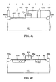
- FIGS. 4 a to 4 i are cross-sections of the method for fabricating S/D devices of the present invention.
- FIG. 5 is a top view of FIG. 4 e;
- FIG. 6 is a top view of FIG. 4 g.
- FIGS. 4 a to 4 i are cross-sections of the method for fabricating S/D devices of the present invention.
- a semiconductor substrate 401 such as silicon, is provided, and a first isolation area 406 a and a second isolation area 406 b are formed thereon.
- a pad layer 402 such as oxide, a conductive layer 403 , such as poly, a hard mask layer 404 , such as nitride or Tetraethylorthosilicate (TEOS), and a first patterned photo resist layer 405 are sequentially formed on the area between the first isolation area 406 a and the second isolation area 406 b .
- the area surrounding by the first isolation area 406 a and the second isolation area 406 b is regarded as an active area (AA).
- the hard mask layer 404 and the conductive layer 403 are sequentially etched to form a gate 403 a using the first patterned photo resist layer 405 as a mask, next, the first patterned photo resist layer 405 is removed, and then, the area of the semiconductor substrate 401 between the gate 403 a and the first isolation area 406 a is doped to form a lightly doped area 407 .
- an insulation layer 408 such as nitride, is conformably formed on the surface of the pad layer 402 and the gate 403 a.
- the insulation layer 408 is isotropically etched to form a spacer 408 a on the sidewall of the gate 403 a.
- a second patterned photo resist layer 409 having a first opening 410 a and a second opening 410 b is formed on the semiconductor substrate 401 .
- the first opening 410 a is positioned on the area between the gate 403 a and the first isolation area 406 a
- the second opening 410 b is positioned on the area spaced between the gate 403 a and the second isolation area 406 b.
- FIG. 5 is the top view of FIG. 4 e .
- part of the active area and half the width of the gate 403 a are exposed by the first opening 410 a in the second patterned photo resist layer 409 .
- a first doped area 411 a is formed at the bottom of the first opening 410 a and a second doped area 411 b is formed at the bottom of the second opening 410 b .
- the second patterned photo resist layer 409 is removed.
- a third patterned photo resist layer 412 having a third opening 413 is formed on the semiconductor substrate 401 , and the width of the gate 403 a exposing because of the third opening 413 in the third patterned photo resist layer 412 is equal to half the width of the gate 403 a .
- the third opening 413 is positioned on the area between the gate 403 a and the second isolation area 406 b.
- Second ion implantation is performed on the semiconductor substrate 401 using the third patterned photo resist layer 412 and the hard mask layer 404 as masks, and the semiconductor substrate 401 is annealed with As or B ions.
- FIG. 6 is a top view of FIG. 4 g .
- part of the active area and the width of the gate 403 a are exposed by the first opening 413 in the third patterned photo resist layer 411 .
- the width of the first opening 413 is equal to half the width of the gate 403 a , and the area between the gate 403 a and the first isolative 406 a is covered with the third patterned photo resist layer 412 .
- a deeply doped area 414 is formed at the bottom of the third opening 413 .
- the third patterned photo resist layer 412 is removed.
- the deeply doped area 414 is 6-7 times the depth of the first doped area 411 a and the second doped area 411 b .
- the deeply doped area 414 expands after annealing, such that the depth and the width of the deeply doped area 414 are both increased.
- the concentration of dopant inside the deeply doped area 414 decreases and the breakdown voltage of the deeply doped area 414 increases accordingly.
- the implantation depth into the substrate can be controlled.
- the width of the third opening 413 is equal to half the width of the gate, the high energy ions do not penetrate through the gate 403 a and the spacer 408 a into the semiconductor substrate 401 because the top layer of the gate 403 a is the hard mask layer 404 .
- the channel between the S/D devices below the gate 403 a and spacer 408 a will not punch through, which means electrons are not injected into the channel from the source region before applying a gate voltage.
- the advantage of the present invention is that the channel between the S/D devices below the gate will not punch through, which means the electric field intensity is reduced to avoid the channel short, and breakdown voltage is increased effectively.
Landscapes
- Insulated Gate Type Field-Effect Transistor (AREA)
Abstract
A method for fabricating source/drain devices. A semiconductor substrate is provided with a gate formed on the semiconductor substrate, and a hard mask layer formed on the gate. A first doped area is formed on a first side of the gate on the semiconductor substrate, and a second doped area is formed on a second side of the gate on the semiconductor substrate in a manner such that the second doped area is separated from the gate by a predetermined distance. A patterned photo resist layer is formed on the semiconductor substrate having an opening on the second side, the exposed gate equal to half the width of the gate. The semiconductor substrate is implanted and annealed to form a dual diffusion area on the second side of the gate using the patterned photo resist layer and the hard mask layer as masks.
Description
This nonprovisional application claims priority under 35 U.S.C. § 119(a) on Patent Application No. 091119777 filed in TAIWAN, R.O.C. on Aug. 30, 2002, which is herein incorporated by reference.
1. Field of the Invention
The invention relates to a semiconductor process, and more particularly to a source/drain (S/D) device fabrication process used in a high voltage circuit element.
2. Description of the Related Art
FIGS. 1a to 1 i are cross-sections of the conventional method for fabricating S/D device.
In FIG. 1a, a semiconductor substrate 101, such as silicon, is provided, and a first isolation area 105 a and a second isolation area 105 b are formed thereon. A pad layer 102, such as oxide, a conductive layer 103, such as poly, and a first patterned photo resist layer 104 are sequentially formed in the area between the first isolation area 105 a and the second isolation area 105 b. The area surrounding the isolation area areas is an active area (AA).
In FIG. 1b, after the conductive layer 103 is etched using the first patterned photo resist layer 104 as a mask to form a gate 103 a, the first patterned photo resist layer 104 is removed. Then, the area of the semiconductor substrate 101 between the gate 103 a and the first isolation area 105 a is doped to form a lightly doped area 106.
In FIG. 1c, an isolating layer 107, such as nitride, is conformably formed on the surface of the pad layer 102 and the gate 103 a.
In FIG. 1d, the isolating layer 107 is isotropically etched to form a spacer 107 a on the sidewall of the gate 103 a.
In FIG. 1e, a second patterned photo resist layer 108 having a first opening 109 a and a second opening 109 b is formed on the semiconductor substrate 101. The first opening 109 a is positioned in the area between the gate 103 a and the first isolation area 105 a, and the second opening 109 b is positioned in the area between the gate 103 a and the second isolation area 105 b.
First ion implantation is performed on the semiconductor substrate 101 using the second patterned photo resist layer 108 as a mask with As or B ions.
FIG. 2 is a top view of FIG. 1e. In FIG. 2, part of the active area and half the width of the gate 103 a are exposed by the first opening 109 a in the second patterned photo resist layer 108.
In FIG. 1f, a first doped area 110 a is formed at the bottom of the first opening 109 a and a second doped area 110 b is formed at the bottom of the second opening 109 b. After the first ion implantation, the second patterned photo resist layer 108 is removed.
In FIG. 1g, a third patterned photo resist layer 111 having a third opening 112 is formed on the semiconductor substrate 101, and half the width of the gate 103 a is exposed by the third opening 112 in the third patterned photo resist layer 111. The third opening 112 is positioned in the area between the gate 103 a and the second isolation area 105 b.
Second ion implantation is performed on the semiconductor substrate 101 using the third patterned photo resist layer 111 as a mask and the semiconductor substrate 101 is annealed with As or B ions.
FIG. 3 is a top view of FIG. 1f. In FIG. 3, part of the active area and half the width of the gate 103 a are exposed by the first opening 112 in the third patterned photo resist layer 111, and the area between the gate 103 a and the first isolating 105 a is covered with the third patterned photo resist layer 111.
In FIG. 1h, a deeply doped area 113 is formed at the bottom of the third opening 112. After the second ion implantation, the third patterned photo resist layer 111 is removed. The deeply doped area 113 is 6-7 times the depth of the first doped area 11 a and the second doped area 110 b. The deeply doped area 113 expands after annealing, such that the depth and the width of the deeply doped area 113 are both increased. When the deeply doped area 113 increases, the concentration of dopant inside the deeply doped area 113 decreases and the breakdown voltage of the deeply doped area 113 increases accordingly.
By varying the energy of the ions to form the deeply doped area 113 in the semiconductor substrate 101, implantation depth into the substrate can be controlled. Meanwhile, the ions also penetrate the gate 103 a and the spacer 107 a into the semiconductor substrate 101, and the size increases after annealing.
The channel between the S/D consisting of the first doped area 110 a and another S/D consisting of the second doped area 110 b and deeply doped area 113 is decreased, resulting in Short Channel Effect. When the two S/D devices are both deeply doped areas, the channel between the S/D devices below the gate 103 a and spacer 107 a punches through, such that electrons are injected into the channel from source region before applying a gate voltage.
The present invention is directed to a method for fabricating source/drain devices in a high voltage circuit element without additional process.
Accordingly, the present invention provides a method for fabricating a source/drain device, in which, first, a semiconductor substrate having a gate is provided. A hard mask layer is formed on the gate. A first doped area is positioned on a first side of the gate on the semiconductor substrate, and a second doped area is positioned on a second side of the gate on the semiconductor substrate and spaced between. A patterned photo resist layer having an opening on the second side of the gate is formed on the semiconductor substrate, and the exposed gate is equal to half the width of the gate. The semiconductor substrate is implanted and annealed to form a dual diffusion area on the second side of the gate using the patterned photo resist layer and the hard mask layer as masks.
Accordingly, the present invention also provides a method for fabricating source/drain devices. A silicon substrate having a gate is provided. A hard mask layer is formed on the gate. A first doped area is positioned on a first side of the gate on the silicon substrate, and a second doped area is positioned on a second side of the gate on the silicon substrate and spaced between. A patterned photo resist layer having an opening on the second side of the gate is formed on the semiconductor substrate, and the width of the exposed gate is equal to half the width of the gate. The silicon substrate is implanted and annealed to form a dual diffusion area on the second side of the gate using the patterned photo resist layer and the hard mask layer as masks.
Accordingly, the present invention also provides a method for fabricating a source/drain device. A semiconductor substrate having a pad layer over the semiconductor substrate, a gate formed on the pad layer, a hard mask layer over the gate, a first isolation area positioned on a first side of the gate, and a second isolation area positioned on a second side of the gate, is provided. The gate has a spacer on the sidewall of the gate. A first patterned photo resist layer is formed. Ions are implanted into the semiconductor substrate to form a first doped area and a second doped area using the patterned photo resist as a mask. The first doped area is positioned between the gate and the first isolation area, and the second doped area is positioned between the gate and second isolation area. A second patterned photo resist layer having an opening on the second side between the gate and the second isolation area is formed on the semiconductor substrate. The width of the exposed gate is equal to half the width of the gate. The semiconductor substrate is implanted and annealed using the patterned photo resist layer and the hard mask layer as masks to form a dual diffusion area on the second side of the gate. The second patterned photo resist layer is removed.
Accordingly, the present invention also provides a method for fabricating a source/drain device. A silicon substrate having a pad oxide layer over the semiconductor substrate, a gate formed on the pad layer, a hard mask layer over the gate, a first isolation area positioned on a first side of the gate, and a second isolation area positioned on a second side of the gate is provided. The gate has a spacer on the sidewall of the gate. A first patterned photo resist layer is formed as a mask to implant the silicon substrate to form a first doped area and a second doped area. The first doped area is positioned between the gate and the first isolation area, and the second doped area is positioned between the gate and second isolation area. The first patterned photo resist layer is removed. A second patterned photoresist layer having an opening on the second side between the gate and the second isolation area is formed on the silicon substrate. The width of the exposed gate is equal to half the width of the gate. The silicon substrate is implanted and annealed using the patterned photo resist layer and the hard mask layer as masks to form a dual diffusion area on the second side of the gate. The second patterned photo resist layer is removed.
For a better understanding of the present invention, reference is made to a detailed description to be read in conjunction with the accompanying drawings, in which:
FIGS. 1a to 1 i are cross-sections of the conventional method for fabricating S/D devices;
FIG. 2 is a top view of FIG. 1e;
FIG. 3 is a top view of FIG. 1g;
FIGS. 4a to 4 i are cross-sections of the method for fabricating S/D devices of the present invention;
FIG. 5 is a top view of FIG. 4e;
FIG. 6 is a top view of FIG. 4g.
FIGS. 4a to 4 i are cross-sections of the method for fabricating S/D devices of the present invention.
In FIG. 4a, first, a semiconductor substrate 401, such as silicon, is provided, and a first isolation area 406 a and a second isolation area 406 b are formed thereon. A pad layer 402, such as oxide, a conductive layer 403, such as poly, a hard mask layer 404, such as nitride or Tetraethylorthosilicate (TEOS), and a first patterned photo resist layer 405 are sequentially formed on the area between the first isolation area 406 a and the second isolation area 406 b. The area surrounding by the first isolation area 406 a and the second isolation area 406 b is regarded as an active area (AA).
In FIG. 4b, the hard mask layer 404 and the conductive layer 403 are sequentially etched to form a gate 403 a using the first patterned photo resist layer 405 as a mask, next, the first patterned photo resist layer 405 is removed, and then, the area of the semiconductor substrate 401 between the gate 403 a and the first isolation area 406 a is doped to form a lightly doped area 407.
In FIG. 4c, an insulation layer 408, such as nitride, is conformably formed on the surface of the pad layer 402 and the gate 403 a.
In FIG. 4d, the insulation layer 408 is isotropically etched to form a spacer 408 a on the sidewall of the gate 403 a.
In FIG. 4e, a second patterned photo resist layer 409 having a first opening 410 a and a second opening 410 b is formed on the semiconductor substrate 401. The first opening 410 a is positioned on the area between the gate 403 a and the first isolation area 406 a, and the second opening 410 b is positioned on the area spaced between the gate 403 a and the second isolation area 406 b.
FIG. 5 is the top view of FIG. 4e. In FIG. 5, part of the active area and half the width of the gate 403 a are exposed by the first opening 410 a in the second patterned photo resist layer 409.
In FIG. 4f, a first doped area 411 a is formed at the bottom of the first opening 410 a and a second doped area 411 b is formed at the bottom of the second opening 410 b. After the first ion implantation, the second patterned photo resist layer 409 is removed.
In FIG. 4g, a third patterned photo resist layer 412 having a third opening 413 is formed on the semiconductor substrate 401, and the width of the gate 403 a exposing because of the third opening 413 in the third patterned photo resist layer 412 is equal to half the width of the gate 403 a. The third opening 413 is positioned on the area between the gate 403 a and the second isolation area 406 b.
Second ion implantation is performed on the semiconductor substrate 401 using the third patterned photo resist layer 412 and the hard mask layer 404 as masks, and the semiconductor substrate 401 is annealed with As or B ions.
FIG. 6 is a top view of FIG. 4g. In FIG. 4, part of the active area and the width of the gate 403 a are exposed by the first opening 413 in the third patterned photo resist layer 411. The width of the first opening 413 is equal to half the width of the gate 403 a, and the area between the gate 403 a and the first isolative 406 a is covered with the third patterned photo resist layer 412.
In FIG. 4h, a deeply doped area 414 is formed at the bottom of the third opening 413. After the second ion implantation, the third patterned photo resist layer 412 is removed. The deeply doped area 414 is 6-7 times the depth of the first doped area 411 a and the second doped area 411 b. The deeply doped area 414 expands after annealing, such that the depth and the width of the deeply doped area 414 are both increased. When the size of the deeply doped area 414 increases, the concentration of dopant inside the deeply doped area 414 decreases and the breakdown voltage of the deeply doped area 414 increases accordingly.
By varying the energy of the ions to form the deeply doped area 414 in the semiconductor substrate 401, the implantation depth into the substrate can be controlled.
When the width of the third opening 413 is equal to half the width of the gate, the high energy ions do not penetrate through the gate 403 a and the spacer 408 a into the semiconductor substrate 401 because the top layer of the gate 403 a is the hard mask layer 404.
When the two SID devices are both deeply doped areas, the channel between the S/D devices below the gate 403 a and spacer 408 a will not punch through, which means electrons are not injected into the channel from the source region before applying a gate voltage.
The advantage of the present invention is that the channel between the S/D devices below the gate will not punch through, which means the electric field intensity is reduced to avoid the channel short, and breakdown voltage is increased effectively.
While the invention has been described by way of example and in terms of the preferred embodiments, it is to be understood that the invention is not limited to the disclosed embodiments. To the contrary, it is intended to cover various modifications and similar arrangements (as would be apparent to those skilled in the art). Therefore, the scope of the appended claims should be accorded the broadest interpretation so as to encompass all such modifications and similar arrangements.
Claims (16)
1. A method for fabricating source/drain devices, comprising:
providing a semiconductor substrate having a gate, a Tetraethylorthosilicate (TEOS) layer over the gate, a first doped area on a first side of the gate on the semiconductor substrate, and a second doped area is on a second side of the gate on the semiconductor substrate with spaces between;
forming a patterned photo resist layer on the semiconductor substrate having an opening on the second side of the gate, wherein the width of the exposed gate is equal to half the width of the gate; and
implanting and annealing the semiconductor substrate to form a dual diffusion area on the second side of the gate using the patterned photo resist layer and the TEOS hard mask layer as masks.
2. The method for fabricating source/drain devices of claim 1 , further comprising removing the patterned photo resist layer.
3. The method for fabricating source/drain devices of claim 1 , wherein the semiconductor substrate further comprises a pad layer.
4. The method for fabricating source/drain devices of claim 3 , wherein the pad layer is an oxide layer.
5. The method for fabricating source/drain devices of claim 1 , wherein the first doped area further comprises a lightly doped area.
6. The method for fabricating source/drain devices of claim 1 , wherein the gate has a spacer on the sidewall of the gate.
7. A method for fabricating source/drain devices, comprising:
providing a silicon substrate having a gate, a Tetraethylorthosilicate (TEOS) layer over the gate, a first doped area on a first side of the gate on the silicon substrate, and a second doped area on a second side of the gate on the silicon substrate with spaces between;
forming a patterned photo resist layer on the semiconductor substrate having an opening on the second side of the gate, wherein the width of the exposed gate is equal to half the width of the gate; and
implanting and annealing the silicon on substrate to form a dual diffusion area on the second side of the gate using the patterned photo resist layer and the TEOS hard mask layer as masks.
8. The method for fabricating source/drain devices of claim 7 , further comprising removing the patterned photo resist layer.
9. The method for fabricating source/drain devices of claim 7 , wherein the semiconductor substrate further comprises a pad oxide layer.
10. The method for fabricating source/drain devices of claim 7 , wherein the first doping area further comprises a lightly doped area.
11. The method for fabricating source/drain devices of claim 7 , wherein the gate has a spacer on the sidewall of the gate.
12. A method for fabricating source/drain devices, comprising:
providing a semiconductor substrate having a pad layer over the semiconductor substrate, a gate formed on the pad oxide layer, a Tetraethylorthosilicate (TEOS) layer over the gate, a first isolation area on a first side of the gate, a second isolation area on a second side of the gate, wherein the gate has a spacer on the sidewall of the gate;
forming a first patterned photo resist layer;
implanting ions into the semiconductor substrate to form a first doped area and a second doped area using the first patterned photo resist layer and the (TEOS) hard mask layer as masks, wherein the first doped area is positioned between the gate and the first isolation area, and the second doped area is positioned between the gate and second isolation area;
removing the first patterned photo resist layer;
forming a second patterned photo resist layer on the semiconductor substrate having an opening on the second side between the gate and the second isolation area, wherein the width of the exposed gate is equal to half the width of the gate;
implanting and annealing the semiconductor substrate using the second patterned photo resist layer as a mask to form a dual diffusion area on the second side of the gate; and
removing the second patterned photo resist layer.
13. The method for fabricating source/drain devices of claim 12 , wherein the pad layer is an oxide layer.
14. The method for fabricating source/drain devices of claim 12 , wherein the first doped area further comprises a lightly doped area.
15. A method for fabricating source/drain devices, comprising:
providing a silicon substrate having a pad oxide layer over the semiconductor substrate, a gate formed on the pad oxide layer, a hard mask layer over the gate, a first isolation area on a first side of the gate, and a second isolation area on a second side of the gate, wherein the gate has a spacer on the sidewall of the gate;
forming a first patterned photo resist layer;
implanting ions into the silicon substrate to form a first doped area and a second doped area using the first patterned photo resist layer and the hard mask layer as masks, wherein the first doped area is between the gate and the first isolation area, and the second doped area is between the gate and second isolation area;
removing the first patterned photo resist layer;
forming a second patterned photo resist layer on the silicon substrate having an opening on the second side between the gate and the second isolation area, wherein the exposed gate is equal to half the width of the gate;
implanting and annealing the silicon substrate using the patterned photo resist layer as a mask to form a dual diffusion area on the second side of the gate; and
removing the second patterned photo resist layer.
16. The method for fabricating source/drain devices of claim 15 , wherein the first doped area further comprises a lightly doped area.
Applications Claiming Priority (3)
| Application Number | Priority Date | Filing Date | Title |
|---|---|---|---|
| TW091119777A TW557481B (en) | 2002-08-30 | 2002-08-30 | Manufacturing method of source/drain device |
| TW91119777A | 2002-08-30 | ||
| TW91119777 | 2002-08-30 |
Publications (2)
| Publication Number | Publication Date |
|---|---|
| US20040043589A1 US20040043589A1 (en) | 2004-03-04 |
| US6835636B2 true US6835636B2 (en) | 2004-12-28 |
Family
ID=31974911
Family Applications (1)
| Application Number | Title | Priority Date | Filing Date |
|---|---|---|---|
| US10/315,980 Expired - Lifetime US6835636B2 (en) | 2002-08-30 | 2002-12-11 | Method for fabricating source/drain devices |
Country Status (2)
| Country | Link |
|---|---|
| US (1) | US6835636B2 (en) |
| TW (1) | TW557481B (en) |
Families Citing this family (2)
| Publication number | Priority date | Publication date | Assignee | Title |
|---|---|---|---|---|
| CN114267735B (en) * | 2020-09-16 | 2026-02-27 | 中芯国际集成电路制造(上海)有限公司 | A semiconductor structure and its formation method |
| CN119384030B (en) * | 2024-02-05 | 2025-09-23 | 芯恩(青岛)集成电路有限公司 | Semiconductor structure and manufacturing method thereof |
Citations (5)
| Publication number | Priority date | Publication date | Assignee | Title |
|---|---|---|---|---|
| US6136686A (en) * | 1997-07-18 | 2000-10-24 | International Business Machines Corporation | Fabrication of interconnects with two different thicknesses |
| US6274468B1 (en) * | 1998-07-06 | 2001-08-14 | United Microelectronics Corp. | Method of manufacturing borderless contact |
| US6391689B1 (en) * | 2001-06-06 | 2002-05-21 | United Microelectronics Corp. | Method of forming a self-aligned thyristor |
| US6690084B1 (en) * | 1997-09-26 | 2004-02-10 | Sanyo Electric Co., Ltd. | Semiconductor device including insulation film and fabrication method thereof |
| US6784047B2 (en) * | 2000-01-14 | 2004-08-31 | Seiko Epson Corporation | Semiconductor devices and methods for manufacturing the same |
-
2002
- 2002-08-30 TW TW091119777A patent/TW557481B/en not_active IP Right Cessation
- 2002-12-11 US US10/315,980 patent/US6835636B2/en not_active Expired - Lifetime
Patent Citations (5)
| Publication number | Priority date | Publication date | Assignee | Title |
|---|---|---|---|---|
| US6136686A (en) * | 1997-07-18 | 2000-10-24 | International Business Machines Corporation | Fabrication of interconnects with two different thicknesses |
| US6690084B1 (en) * | 1997-09-26 | 2004-02-10 | Sanyo Electric Co., Ltd. | Semiconductor device including insulation film and fabrication method thereof |
| US6274468B1 (en) * | 1998-07-06 | 2001-08-14 | United Microelectronics Corp. | Method of manufacturing borderless contact |
| US6784047B2 (en) * | 2000-01-14 | 2004-08-31 | Seiko Epson Corporation | Semiconductor devices and methods for manufacturing the same |
| US6391689B1 (en) * | 2001-06-06 | 2002-05-21 | United Microelectronics Corp. | Method of forming a self-aligned thyristor |
Also Published As
| Publication number | Publication date |
|---|---|
| TW557481B (en) | 2003-10-11 |
| US20040043589A1 (en) | 2004-03-04 |
Similar Documents
| Publication | Publication Date | Title |
|---|---|---|
| US5413949A (en) | Method of making self-aligned MOSFET | |
| KR100794094B1 (en) | Method of manufacturing transistor of semiconductor device | |
| US7550352B2 (en) | MOS transistor having a recessed gate electrode and fabrication method thereof | |
| KR20020067795A (en) | Method of fabricating Metal Oxide Semiconductor transistor with Lightly Doped Drain structure | |
| JPH0575115A (en) | Semiconductor device and manufacturing method thereof | |
| US20090011561A1 (en) | Method of fabricating high-voltage mos having doubled-diffused drain | |
| US6709939B2 (en) | Method for fabricating semiconductor device | |
| KR100801729B1 (en) | Transistor having recessed gate structure and manufacturing method | |
| US6562686B2 (en) | Method for fabricating semiconductor device | |
| US6008100A (en) | Metal-oxide semiconductor field effect transistor device fabrication process | |
| US6713338B2 (en) | Method for fabricating source/drain devices | |
| US20090096023A1 (en) | Method for manufacturing semiconductor device | |
| US6268256B1 (en) | Method for reducing short channel effect | |
| US6835636B2 (en) | Method for fabricating source/drain devices | |
| KR100343469B1 (en) | Fabricating method of transistor | |
| JP3714396B2 (en) | Manufacturing method of semiconductor device | |
| KR100552848B1 (en) | Manufacturing Method of Morse Field Effect Transistor Using Selective Silicide Process | |
| KR20040002211A (en) | Semiconductor device and method for fabricating the same | |
| KR101102775B1 (en) | Manufacturing Method of Semiconductor Device | |
| KR100937650B1 (en) | Transistor manufacturing method of semiconductor device | |
| KR100247170B1 (en) | Tr fabricating method having tranch | |
| KR100641482B1 (en) | Semiconductor gate line formation method | |
| KR100900234B1 (en) | Semiconductor device and manufacturing method thereof | |
| KR100607731B1 (en) | Semiconductor gate line formation method | |
| KR100546812B1 (en) | Semiconductor device manufacturing method |
Legal Events
| Date | Code | Title | Description |
|---|---|---|---|
| AS | Assignment |
Owner name: VANGUARD INTERNATIONAL SEMICONDUCTOR CORPORATION, Free format text: ASSIGNMENT OF ASSIGNORS INTEREST;ASSIGNORS:JAN, YI-TSUNG;WANG, WEN-TSUNG;WEI, SUNG-MIN;AND OTHERS;REEL/FRAME:013562/0850 Effective date: 20021119 |
|
| STCF | Information on status: patent grant |
Free format text: PATENTED CASE |
|
| FPAY | Fee payment |
Year of fee payment: 4 |
|
| FPAY | Fee payment |
Year of fee payment: 8 |
|
| FPAY | Fee payment |
Year of fee payment: 12 |