US6818357B2 - Photolithographic mask fabrication - Google Patents
Photolithographic mask fabrication Download PDFInfo
- Publication number
- US6818357B2 US6818357B2 US09/969,156 US96915601A US6818357B2 US 6818357 B2 US6818357 B2 US 6818357B2 US 96915601 A US96915601 A US 96915601A US 6818357 B2 US6818357 B2 US 6818357B2
- Authority
- US
- United States
- Prior art keywords
- mask
- refraction
- index
- absorber
- thin layer
- Prior art date
- Legal status (The legal status is an assumption and is not a legal conclusion. Google has not performed a legal analysis and makes no representation as to the accuracy of the status listed.)
- Expired - Fee Related, expires
Links
- 238000004519 manufacturing process Methods 0.000 title claims description 12
- 239000006096 absorbing agent Substances 0.000 claims abstract description 102
- 238000000034 method Methods 0.000 claims abstract description 89
- 239000000463 material Substances 0.000 claims abstract description 68
- 238000003384 imaging method Methods 0.000 claims abstract description 65
- 239000000758 substrate Substances 0.000 claims abstract description 37
- 230000008569 process Effects 0.000 claims abstract description 36
- 238000000206 photolithography Methods 0.000 claims abstract description 26
- 230000005855 radiation Effects 0.000 claims description 72
- 238000005530 etching Methods 0.000 claims description 26
- 238000000151 deposition Methods 0.000 claims description 16
- 229910052710 silicon Inorganic materials 0.000 claims description 14
- 239000010703 silicon Substances 0.000 claims description 13
- 238000002310 reflectometry Methods 0.000 claims description 12
- 229910052782 aluminium Inorganic materials 0.000 claims description 10
- XAGFODPZIPBFFR-UHFFFAOYSA-N aluminium Chemical compound [Al] XAGFODPZIPBFFR-UHFFFAOYSA-N 0.000 claims description 10
- 230000001419 dependent effect Effects 0.000 claims description 9
- 239000000203 mixture Substances 0.000 claims description 9
- 229910052707 ruthenium Inorganic materials 0.000 claims description 8
- KJTLSVCANCCWHF-UHFFFAOYSA-N Ruthenium Chemical compound [Ru] KJTLSVCANCCWHF-UHFFFAOYSA-N 0.000 claims description 7
- 229910052750 molybdenum Inorganic materials 0.000 claims description 6
- 230000008439 repair process Effects 0.000 claims description 6
- 238000004544 sputter deposition Methods 0.000 claims description 6
- ZOKXTWBITQBERF-UHFFFAOYSA-N Molybdenum Chemical compound [Mo] ZOKXTWBITQBERF-UHFFFAOYSA-N 0.000 claims description 5
- XUIMIQQOPSSXEZ-UHFFFAOYSA-N Silicon Chemical compound [Si] XUIMIQQOPSSXEZ-UHFFFAOYSA-N 0.000 claims description 5
- GNKTZDSRQHMHLZ-UHFFFAOYSA-N [Si].[Si].[Si].[Ti].[Ti].[Ti].[Ti].[Ti] Chemical compound [Si].[Si].[Si].[Ti].[Ti].[Ti].[Ti].[Ti] GNKTZDSRQHMHLZ-UHFFFAOYSA-N 0.000 claims description 5
- 229910052732 germanium Inorganic materials 0.000 claims description 5
- GNPVGFCGXDBREM-UHFFFAOYSA-N germanium atom Chemical compound [Ge] GNPVGFCGXDBREM-UHFFFAOYSA-N 0.000 claims description 5
- 239000011733 molybdenum Substances 0.000 claims description 5
- 239000005368 silicate glass Substances 0.000 claims description 5
- 238000001311 chemical methods and process Methods 0.000 claims 2
- 239000004065 semiconductor Substances 0.000 abstract description 12
- 238000000059 patterning Methods 0.000 abstract description 2
- VYPSYNLAJGMNEJ-UHFFFAOYSA-N Silicium dioxide Chemical compound O=[Si]=O VYPSYNLAJGMNEJ-UHFFFAOYSA-N 0.000 description 20
- 229920002120 photoresistant polymer Polymers 0.000 description 18
- 238000004088 simulation Methods 0.000 description 18
- MZLGASXMSKOWSE-UHFFFAOYSA-N tantalum nitride Chemical compound [Ta]#N MZLGASXMSKOWSE-UHFFFAOYSA-N 0.000 description 15
- 238000001900 extreme ultraviolet lithography Methods 0.000 description 11
- 239000000377 silicon dioxide Substances 0.000 description 10
- 230000010363 phase shift Effects 0.000 description 9
- 230000000694 effects Effects 0.000 description 8
- 239000011651 chromium Substances 0.000 description 5
- 229910000577 Silicon-germanium Inorganic materials 0.000 description 4
- 238000010521 absorption reaction Methods 0.000 description 4
- 239000007789 gas Substances 0.000 description 4
- LEVVHYCKPQWKOP-UHFFFAOYSA-N [Si].[Ge] Chemical compound [Si].[Ge] LEVVHYCKPQWKOP-UHFFFAOYSA-N 0.000 description 3
- 229910045601 alloy Inorganic materials 0.000 description 3
- 239000000956 alloy Substances 0.000 description 3
- 238000001020 plasma etching Methods 0.000 description 3
- VYZAMTAEIAYCRO-UHFFFAOYSA-N Chromium Chemical compound [Cr] VYZAMTAEIAYCRO-UHFFFAOYSA-N 0.000 description 2
- 229910000676 Si alloy Inorganic materials 0.000 description 2
- CSDREXVUYHZDNP-UHFFFAOYSA-N alumanylidynesilicon Chemical compound [Al].[Si] CSDREXVUYHZDNP-UHFFFAOYSA-N 0.000 description 2
- 229910052804 chromium Inorganic materials 0.000 description 2
- 230000003247 decreasing effect Effects 0.000 description 2
- 238000010586 diagram Methods 0.000 description 2
- 238000005240 physical vapour deposition Methods 0.000 description 2
- 235000012239 silicon dioxide Nutrition 0.000 description 2
- 229910052582 BN Inorganic materials 0.000 description 1
- OKTJSMMVPCPJKN-UHFFFAOYSA-N Carbon Chemical compound [C] OKTJSMMVPCPJKN-UHFFFAOYSA-N 0.000 description 1
- 230000002238 attenuated effect Effects 0.000 description 1
- 238000005452 bending Methods 0.000 description 1
- 230000008901 benefit Effects 0.000 description 1
- XTDAIYZKROTZLD-UHFFFAOYSA-N boranylidynetantalum Chemical compound [Ta]#B XTDAIYZKROTZLD-UHFFFAOYSA-N 0.000 description 1
- 229910052799 carbon Inorganic materials 0.000 description 1
- 230000008859 change Effects 0.000 description 1
- 150000001875 compounds Chemical class 0.000 description 1
- 230000008021 deposition Effects 0.000 description 1
- 239000002223 garnet Substances 0.000 description 1
- 239000011521 glass Substances 0.000 description 1
- 238000007689 inspection Methods 0.000 description 1
- 230000003993 interaction Effects 0.000 description 1
- 230000004048 modification Effects 0.000 description 1
- 238000012986 modification Methods 0.000 description 1
- 230000003287 optical effect Effects 0.000 description 1
- 230000000737 periodic effect Effects 0.000 description 1
- 230000009467 reduction Effects 0.000 description 1
- 238000000985 reflectance spectrum Methods 0.000 description 1
- 229910021332 silicide Inorganic materials 0.000 description 1
- 229910052715 tantalum Inorganic materials 0.000 description 1
- GUVRBAGPIYLISA-UHFFFAOYSA-N tantalum atom Chemical compound [Ta] GUVRBAGPIYLISA-UHFFFAOYSA-N 0.000 description 1
- 229910052724 xenon Inorganic materials 0.000 description 1
- FHNFHKCVQCLJFQ-UHFFFAOYSA-N xenon atom Chemical compound [Xe] FHNFHKCVQCLJFQ-UHFFFAOYSA-N 0.000 description 1
Images




Classifications
-
- B—PERFORMING OPERATIONS; TRANSPORTING
- B82—NANOTECHNOLOGY
- B82Y—SPECIFIC USES OR APPLICATIONS OF NANOSTRUCTURES; MEASUREMENT OR ANALYSIS OF NANOSTRUCTURES; MANUFACTURE OR TREATMENT OF NANOSTRUCTURES
- B82Y10/00—Nanotechnology for information processing, storage or transmission, e.g. quantum computing or single electron logic
-
- G—PHYSICS
- G03—PHOTOGRAPHY; CINEMATOGRAPHY; ANALOGOUS TECHNIQUES USING WAVES OTHER THAN OPTICAL WAVES; ELECTROGRAPHY; HOLOGRAPHY
- G03F—PHOTOMECHANICAL PRODUCTION OF TEXTURED OR PATTERNED SURFACES, e.g. FOR PRINTING, FOR PROCESSING OF SEMICONDUCTOR DEVICES; MATERIALS THEREFOR; ORIGINALS THEREFOR; APPARATUS SPECIALLY ADAPTED THEREFOR
- G03F1/00—Originals for photomechanical production of textured or patterned surfaces, e.g., masks, photo-masks, reticles; Mask blanks or pellicles therefor; Containers specially adapted therefor; Preparation thereof
- G03F1/22—Masks or mask blanks for imaging by radiation of 100nm or shorter wavelength, e.g. X-ray masks, extreme ultraviolet [EUV] masks; Preparation thereof
-
- B—PERFORMING OPERATIONS; TRANSPORTING
- B82—NANOTECHNOLOGY
- B82Y—SPECIFIC USES OR APPLICATIONS OF NANOSTRUCTURES; MEASUREMENT OR ANALYSIS OF NANOSTRUCTURES; MANUFACTURE OR TREATMENT OF NANOSTRUCTURES
- B82Y40/00—Manufacture or treatment of nanostructures
-
- G—PHYSICS
- G03—PHOTOGRAPHY; CINEMATOGRAPHY; ANALOGOUS TECHNIQUES USING WAVES OTHER THAN OPTICAL WAVES; ELECTROGRAPHY; HOLOGRAPHY
- G03F—PHOTOMECHANICAL PRODUCTION OF TEXTURED OR PATTERNED SURFACES, e.g. FOR PRINTING, FOR PROCESSING OF SEMICONDUCTOR DEVICES; MATERIALS THEREFOR; ORIGINALS THEREFOR; APPARATUS SPECIALLY ADAPTED THEREFOR
- G03F1/00—Originals for photomechanical production of textured or patterned surfaces, e.g., masks, photo-masks, reticles; Mask blanks or pellicles therefor; Containers specially adapted therefor; Preparation thereof
- G03F1/22—Masks or mask blanks for imaging by radiation of 100nm or shorter wavelength, e.g. X-ray masks, extreme ultraviolet [EUV] masks; Preparation thereof
- G03F1/24—Reflection masks; Preparation thereof
-
- G—PHYSICS
- G03—PHOTOGRAPHY; CINEMATOGRAPHY; ANALOGOUS TECHNIQUES USING WAVES OTHER THAN OPTICAL WAVES; ELECTROGRAPHY; HOLOGRAPHY
- G03F—PHOTOMECHANICAL PRODUCTION OF TEXTURED OR PATTERNED SURFACES, e.g. FOR PRINTING, FOR PROCESSING OF SEMICONDUCTOR DEVICES; MATERIALS THEREFOR; ORIGINALS THEREFOR; APPARATUS SPECIALLY ADAPTED THEREFOR
- G03F1/00—Originals for photomechanical production of textured or patterned surfaces, e.g., masks, photo-masks, reticles; Mask blanks or pellicles therefor; Containers specially adapted therefor; Preparation thereof
- G03F1/38—Masks having auxiliary features, e.g. special coatings or marks for alignment or testing; Preparation thereof
-
- G—PHYSICS
- G03—PHOTOGRAPHY; CINEMATOGRAPHY; ANALOGOUS TECHNIQUES USING WAVES OTHER THAN OPTICAL WAVES; ELECTROGRAPHY; HOLOGRAPHY
- G03F—PHOTOMECHANICAL PRODUCTION OF TEXTURED OR PATTERNED SURFACES, e.g. FOR PRINTING, FOR PROCESSING OF SEMICONDUCTOR DEVICES; MATERIALS THEREFOR; ORIGINALS THEREFOR; APPARATUS SPECIALLY ADAPTED THEREFOR
- G03F1/00—Originals for photomechanical production of textured or patterned surfaces, e.g., masks, photo-masks, reticles; Mask blanks or pellicles therefor; Containers specially adapted therefor; Preparation thereof
- G03F1/54—Absorbers, e.g. of opaque materials
-
- G—PHYSICS
- G03—PHOTOGRAPHY; CINEMATOGRAPHY; ANALOGOUS TECHNIQUES USING WAVES OTHER THAN OPTICAL WAVES; ELECTROGRAPHY; HOLOGRAPHY
- G03F—PHOTOMECHANICAL PRODUCTION OF TEXTURED OR PATTERNED SURFACES, e.g. FOR PRINTING, FOR PROCESSING OF SEMICONDUCTOR DEVICES; MATERIALS THEREFOR; ORIGINALS THEREFOR; APPARATUS SPECIALLY ADAPTED THEREFOR
- G03F1/00—Originals for photomechanical production of textured or patterned surfaces, e.g., masks, photo-masks, reticles; Mask blanks or pellicles therefor; Containers specially adapted therefor; Preparation thereof
- G03F1/26—Phase shift masks [PSM]; PSM blanks; Preparation thereof
Definitions
- This invention relates to fabrication of photolithographic masks for semiconductor processing.
- Photolithography uses an imaging system that directs radiation onto a patterned mask to form an image that then is projected onto a semiconductor wafer covered with light-sensitive photoresist.
- FIG. 1 is a block diagram of a photolithography imaging system that uses a mask in processing a wafer.
- FIGS. 2A-2E are cross-sectional representations of a mask at different phases of a fabrication process.
- FIGS. 3A and 3B are graphs of the critical dimension of a wafer versus de-focus of the imaging system for, respectively, dense and isolated features of the mask fabricated using the process of FIGS. 2A-2E.
- FIGS. 4A-4G are cross-sectional representations of a mask at different phases of a fabrication process in which a thin layer is deposited on a reflector of the mask.
- FIG. 4H is a cross-sectional representation of reflection at an interface between the thin layer and the reflector in the mask fabricated using the process of FIGS. 4A-4G.
- FIG. 5 is a graph of reflectivity of the mask versus a thickness of the thin layer in the mask fabricated using the process of FIGS. 4A-4G.
- FIG. 6 is a graph of the critical dimension of a wafer versus de-focus of the imaging system for isolated features of the mask fabricated using the process of FIGS. 4A-4G.
- FIGS. 7A-7G are cross-sectional representations of a mask at different phases of a fabrication process in which a trench is etched into a reflector of the mask.
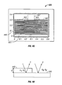
- FIG. 8 is a photograph of a mask fabricated using the process of FIGS. 7A-7G.
- FIGS. 9A and 9B are graphs of the critical dimension of a wafer versus de-focus of the imaging system for, respectively, dense and isolated features of the mask fabricated using the process of FIGS. 7A-7G.
- FIG. 10 is a diagram showing a shadowing effect during photolithography.
- FIG. 11 is a graph of the critical dimension of a wafer versus the critical dimension of a mask patterned to image the wafer.
- FIGS. 12A and 12B are graphs of the critical dimension of a wafer versus de-focus of the imaging system for, respectively, dense and isolated features of the mask fabricated with an absorber made of germanium using the process of FIGS. 2A-2E.
- FIGS. 13A and 13B are graphs of the critical dimension of a wafer versus de-focus of the imaging system for, respectively, dense and isolated features of the mask fabricated with an absorber made of aluminum using the process of FIGS. 2A-2E.
- FIGS. 14A and 14B are graphs of the critical dimension of a wafer versus de-focus of the imaging system for, respectively, dense and isolated features of the mask fabricated with an absorber made of aluminum and a buffer made of silicon-germanium alloy using the process of FIGS. 2 A- 2 E.
- Photolithography uses an imaging system that directs radiation onto a mask to form a pattern and then projects the image of that pattern, for example, with a reduction of 4:1, onto a semiconductor wafer covered with light-sensitive photoresist.
- the radiation used in photolithography may be at any suitable wavelength, with the resolution of the system improving with decreasing wavelength. As resolution improves, the ability to print smaller features onto the semiconductor wafer improves.
- EUV radiation in the extreme ultraviolet (EUV) wavelength range.
- EUV radiation has wavelengths in the range of 1 to 40 nanometers (nm)
- the EUV radiation used in photolithography has wavelengths in the range of 10 to 14 nm.
- Photolithography carried out with radiation in this region has come to be known as EUV lithography (EUVL).
- an EUVL imaging system 100 includes a radiation source 105 , a condenser optics section 110 , a projection optics section 112 , a mask stage 115 , and a wafer stage 120 .
- EUVL imaging systems For ease of discussion, the implementations that are discussed relate to EUVL imaging systems. However, the methods and systems described are not limited to EUVL imaging systems. Rather, they may be used in any photolithography imaging system that uses a mask, and in some instances, a reflective mask. They also may be used in a photolithography imaging system that uses a transmissive mask.
- the radiation source 105 may be any source able to produce radiation in the extreme ultraviolet (EUV) wavelength range.
- a suitable radiation source 105 is a plasma created when a laser, such as a 1700 Watt (W) pulsed ytterbium-aluminum-garnet (YAG) solid-state laser, illuminates a gas, such as a supersonic jet of xenon gas.
- a suitable radiation source 105 may be formed using bending magnets and undulators associated with synchrotrons.
- a suitable radiation source 105 may be formed or developed from discharge sources, which have the potential to provide adequate power in the desired wavelength range.
- EUV radiation is strongly absorbed in virtually all transmissive materials, including gases and glass. For this reason, EUV imaging is carried out in a near vacuum.
- the mask stage 115 includes a mask 125 mounted to a transport stage 130 that scans the mask 125 .
- the mask 125 may be planar, concave, convex, or any suitable shape to permit patterning.
- the mask 125 is reflective because EUW radiation is strongly absorbed in transmissive materials such as lenses, which may be used in traditional photolithography imaging systems.
- the wafer stage 120 includes a photoresist-coated semiconductor wafer 135 mounted to a transport stage 140 that scans the wafer 135 in synchrony with the mask 125 and steps the wafer 135 into a position to accept a next image from the mask 125 .
- the condenser optics section 110 brings the radiation from the source 105 to the mask stage 115 .
- the condenser optics are reflective because of the absorption associated with EUV radiation.
- the condenser optics section 110 includes condenser reflectors or mirrors 145 that collect and focus the radiation from the source 105 onto the mask stage 115 . Any number of condenser mirrors 145 may be used, such as, for example, the four shown in FIG. 1 .
- the projection optics section 112 reduces the image from the mask 125 in the mask stage 115 and forms the image onto wafer 135 in the wafer stage 120 .
- the projection optics are reflective because of the absorption associated with EUV radiation.
- the projection optics section 112 includes reflectors or mirrors 150 that project radiation reflected from the mask 125 onto the wafer.
- the reflectance spectrum of the mask 125 may be matched to that of the mirrors in the projection optics section 112 .
- a reflective mask 225 (FIGS. 2D and 2E) includes a patterned absorber 230 that absorbs EUV radiation, a buffer 235 , a multilayer (ML) reflector 240 , and an underlying mask blank 241 .
- the mask blank 241 may be any substrate that can handle subsequent fabrication processes and is typically made of a material having a low thermal expansion, such as, for example, ULETM, an ultralow expansion titanium silicate glass made by Corning Corporation of New York. In one implementation the mask blank 241 , is 0.64 cm thick. In operation, any radiation incident on the mask 225 (represented by arrow 250 in FIG. 2D) will be absorbed by the patterned absorber 230 or partially reflected (represented by arrow 255 in FIG. 2D) by the ML reflector 240 in the non-patterned region.
- the ML reflector 240 is formed on the mask blank 241 and generally consists of multiple layers of alternating reflecting material and transmissive material that provide a resonant reflectivity when the period of the layers is approximately one half the wavelength of the radiation used in the imaging system.
- the materials are molybdenum (Mo) and silicon (Si), which are alternately layered at thicknesses of about 2 to 12 nm to create a ML reflector thickness of about 50 to 500 nm.
- the buffer 235 may be any material that serves as a stop layer or an etch profile controller.
- the buffer 235 protects the underlying reflector during mask etching and repair while ensuring that etched patterns in the absorber are clean and substantially vertical.
- the buffer 235 is relatively non-opaque and should be easy to selectively remove or etch.
- the thickness of the buffer 235 is mostly determined by absorber etch selectivity to the buffer, repair etch selectivity to the ML reflector, and optical inspection contrast.
- the buffer 235 has a thickness ranging from 30 to 50 nm and is made of silicon dioxide (SiO 2 ).
- the buffer may be made of carbon (C) or ruthenium (Ru).
- the absorber 230 may be any suitable material that is absorptive of radiation at the wavelength used in the imaging system 100 and that can be selectively etched.
- the thickness of the absorber 230 is mostly determined by the radiation absorption of the material used as the absorber.
- the absorber 230 may be made of any material or composition that meets these criteria, such as, for example, chromium (Cr), tantalum (Ta), tantalum nitride (TaN), and tantalum boron nitride (TaBN).
- Cr chromium
- Ta tantalum
- TaN tantalum nitride
- TaBN tantalum boron nitride
- the thickness of the absorber 230 may be in the range of 50 to 100 nm.
- the mask 225 is formed by depositing the ML reflector 240 on the mask blank 241 .
- the buffer 235 is placed on top of the ML reflector 240 using any suitable technique such as physical vapor deposition or sputtering techniques. The technique is performed at a temperature selected to avoid modification to the underlying ML reflector 240 .
- the absorber 230 is placed on top of the buffer 235 using any suitable technique such as physical vapor deposition or sputtering techniques.
- the mask 225 is etched using any suitable etching technique.
- a layer of photoresist 245 is patterned on top of the absorber 230 and that pattern is replicated into the absorber 230 by etching the absorber 230 in locations not covered by the photoresist 245 to form the mask features 247 .
- the photoresist 245 then is selectively removed and the buffer 235 is etched in locations not covered by the absorber 230 to produce the mask shown in FIGS. 2D and 2E.
- the etched mask pattern ultimately is used to pattern the semiconductor wafer using the projection optics and the condenser optics, as discussed above.
- the mask is etched using plasma etching.
- the mask 225 is characterized by its critical dimensions (CD), which are typically the line widths of the features.
- CD critical dimensions
- One feature is separated from an adjacent feature by a space and the pitch or period is the distance from a point on a feature to the same point on an adjacent feature or the line width plus the space.
- Periodic or dense features of the mask are defined to be those features of the mask in which the line width is equal to the spacing between the features.
- dense features may have a 30 nm line width and a 60 nm pitch.
- Isolated or semi-isolated features of the mask are defined as those features of the mask in which the line width is less than the spacing between features.
- isolated features may have a 30 nm line width and a 200 nm pitch.
- the features of the mask are imaged onto the wafer such that the wafer is also characterized by its own critical dimensions, which are proportional to, though generally smaller than, the critical dimensions of the mask.
- one problem often encountered in photolithography is a conflict between the conditions needed for proper printing of the isolated features and the conditions needed for proper printing of the dense features. That conflict may be realized or understood when analyzing how the line width of the wafer features varies as the imaging system is de-focused.
- phase error may be induced at the boundary between the mask reflector (such as reflector 240 ) and the absorber (such as absorber 230 ).
- a phase error is caused by the interaction of the radiation reflected from the mask reflector and the radiation scattered at the boundary between the absorber and the reflector.
- the induced phase error causes a pitch-dependent shift in focus, where focus is a characteristic of the imaging system.
- the phase error also causes a process window tilt that is exhibited in the isolated features.
- the process window is the range of focus and exposure dose of the imaging system that produces an adequate or useful wafer.
- the effect of pitch-dependent focus shift and process window tilt greatly reduces the common process window for the dense and isolated features.
- FIG. 3A shows a graph 300 of the line width 305 (in micrometers or ⁇ m) of the wafer versus de-focus 310 (in ⁇ m) of the imaging system for dense features of the mask having a width of 30 nm.
- FIG. 3B shows a graph 350 of the line width 355 (in ⁇ m) of the wafer versus de-focus 360 (in ⁇ m) for isolated features of the mask having a width of 30 nm.
- the graphs 300 , 350 are outputs of a simulation of the performance of the mask 225 .
- the structure of the mask 225 is such that the substrate is made of SiO 2 having a thickness of 28 nm, the reflector 240 is made of Mo/Si stack in which the Mo has a thickness of 2.76 nm and the Si has a thickness of 4.14 nm, the buffer layer is eliminated, and the absorber is made of TaN at a thickness of 100 nm.
- the radiation wavelength is 13.42 nm
- the numerical aperture of the imaging system is 0.25
- the angle of incidence ( ⁇ ) of the radiation, relative to the normal to the surface of, for example, the mask is 5°.
- the shapes of the graphs 300 , 350 depend on the exposure dose of the radiation to the wafer. As is evident from the graphs 300 , 350 , there exists a shift in focus from the isolated features in FIG. 3B relative to the dense features in FIG. 3 A. Moreover, the process window for the isolated features in FIG. 3B is asymmetric or tilted. Because of these problems, the common process window for both the isolated and the dense features is reduced.
- an opposite phase shift may be induced during fabrication of the mask to compensate for the phase error, as discussed below.
- a mask 425 may be formed with a thin layer 442 deposited as an additional top layer on ML reflector 440 . During etching, the thin layer 442 is removed at portions 443 adjacent the features of the mask. The material for the thin layer is selected to offset the phase shift.
- the mask is prepared by depositing the ML reflector 440 on a mask blank 441 , depositing the thin layer 442 on the reflector 440 , depositing a buffer 435 on the thin layer 442 , and depositing an absorber 430 on the buffer 435 . Examples of deposition techniques are discussed above with respect to FIG. 2 A.
- a photoresist 445 is patterned on top of the absorber 430 and, as shown in FIG. 4C, that pattern is replicated into the absorber 430 by etching the absorber 430 in locations not covered by the photoresist 445 to form the mask features 447 .
- the photoresist 445 is selectively removed and the buffer 435 is etched in locations not covered by the absorber 430 .
- another photoresist 455 is patterned on top of the thin layer 442 .
- the pattern is replicated into the thin layer 442 by etching the thin layer 442 in locations not covered by the photoresist 455 or the absorber 430 and then selectively removing the photoresist 455 to form the mask 425 .
- the etched mask pattern ultimately will be used to to pattern the semiconductor wafer using the projection optics and the condenser optics, as discussed above.
- the mask is etched using plasma etching.
- ⁇ is the wavelength of the radiation from the radiation source
- ⁇ n is n 1 ⁇ n v
- n 1 is the real part of the index of refraction of the thin layer
- n v is the real part of the index of refraction of vacuum
- ⁇ is the angle of incidence of the radiation from the radiation source
- d is the thickness of the thin layer.
- the thin layer is made of silicon dioxide (SiO 2 )
- SiO 2 silicon dioxide
- a thickness d of 16 nm is required to obtain a phase correction of 18°. As a result, light would be attenuated by the thick layer of SiO 2 .
- Other possible materials that may be used for the thin layer 442 include, for example, Mo, moly-silicide (MoSi), or any other materials that produce a phase correction without an unacceptable amount of light attenuation.
- the thin layer 442 is etched at locations adjacent to the absorber feature 447 . If the thin layer is made of 3 mm thick Ru, and if the Ru is etched to have a width of 5 nm to 20 nm (1 ⁇ ) near the edge of the feature 447 , a phase error (10 to 30 degrees) at the feature edge is generated. This phase error has the opposite sign as the phase error induced in the EUVL imaging system 100 and responsible for the pattern pitch-dependent focus shift. The two phase errors therefore cancel each other and pitch-dependent focus shift is corrected.
- FIG. 5 shows a graph 500 of mask reflectivity relative to the thickness of a thin layer made of Ru deposited on an ML reflector 440 made of 40 pairs of Mo/Si layers.
- the Ru layer thickness 505 increases above 3 nm, the mask reflectivity reduces significantly.
- the Ru layer generally should have a thickness 505 less than or equal to 4 nm.
- the reflectivity levels off to 0.75 with a Ru layer having a thickness 505 less than 3 nm.
- the Ru may be etched to have a width of 5 nm to 30 nm (1 ⁇ ) near the edge of the feature to obtain a suitable phase error.
- FIG. 6 shows simulation results (graph 600 ) of mask performance for the mask 425 . These results show the line width 605 (in ⁇ m) versus de-focus 610 (in ⁇ m) for various exposure doses.
- the structure of the mask 425 is such that the substrate is made of SiO 2 having a thickness of 28 nm, the reflector 440 is made of Mo/Si stack in which the Mo has a thickness of 2.76 nm and the Si has a thickness of 4.14, the buffer layer is eliminated, the absorber is made of TaN at a thickness of 100 nm, and the thin layer 442 is made of Ru having a thickness of 3 nm.
- the radiation wavelength is 13.42 nm
- the numerical aperture of the imaging system is 0.25
- the angle of incidence ⁇ of the radiation is 5°.
- the simulated etched width on each side of the mask feature 447 is 16 nm at 1 ⁇ scale, or 64 nm at the 4 ⁇ mask scale.
- a mask 725 or 765 may be formed in which trenches are etched directly into portions 743 of the reflector 740 that are adjacent the features of the mask. In this way, a phase shift is created directly from the partially-etched reflector 740 .
- the mask 725 or 765 includes a ML reflector 740 deposited on a mask blank 741 , a buffer 735 placed on the ML reflector 740 , and an absorber 730 placed on the buffer 735 . Initially, as shown in FIG.
- the mask is prepared by depositing the ML reflector 740 on the mask blank 741 , depositing the buffer 735 on the reflector 740 , and depositing the absorber 730 on the buffer 735 .
- Particular deposition techniques are discussed above with respect to FIG. 2 A. Because the reflector 740 will be etched, it is advantageous to add a few extra layers to the ML reflector in the deposition of the ML reflector.
- a photoresist 745 is patterned on the absorber 730 and, as shown in FIG. 7C, that pattern is replicated into the absorber 730 by etching the absorber 730 in locations not covered by the photoresist 745 to form the mask features 747 .
- the photoresist 745 is selectively removed and the buffer 735 is etched in locations not covered by the absorber 730 .
- two ways of etching the buffer 735 include etching the buffer in the traditional manner (A) or etching the buffer so that a trench 739 is formed in the reflector 740 (B). This may be accomplished by etching the buffer faster at the edge of the feature 747 than at other locations along the buffer (a process referred to as micro-trenching).
- the buffer is etched according to the second manner (FIG. 7 D-B)
- no additional resist processes are required and the mask 765 is formed.
- the trench 739 is visible in a photograph of a portion 800 of a mask 765 made using the process shown in FIGS. 7A-7D.
- the buffer is etched according to the first manner (FIG. 7 D-A), then, as shown in FIG. 7E, another photoresist 755 is patterned on top of the reflector 740 .
- the pattern is replicated into the reflector 740 by etching the reflector 740 (through, for example, about 4 pairs of the ML) in locations not covered by the photoresist 755 or the absorber 730 and then photoresist 755 is selectively removed to form the mask 725 .
- the etched mask pattern ultimately will be used to pattern the semiconductor wafer using the projection optics and the condenser optics, as discussed above. In one implementation, as discussed above, the mask is etched using plasma etching.
- ⁇ is the wavelength of the radiation from the radiation source
- ⁇ n 1 is n 1 ⁇ n v
- n 1 is the real part of the index of refraction of the reflector 740 and n v is the real part of the index of refraction of vacuum
- d 1 is the thickness of the layer in the multilayer reflector.
- simulation results show the line width (in ⁇ m) 905 versus de-focus (in ⁇ m) 910 for various exposure doses of the dense features and the line width (in ⁇ m) 915 versus de-focus (in ⁇ m) 920 for various exposure doses of the isolated features.
- the structure of the mask 765 is such that the substrate is made of SiO 2 having a thickness of 28 nm, the reflector 740 is made of Mo/Si stack in which the Mo has a thickness of 2.76 nm and the Si has a thickness of 4.14, the buffer layer is eliminated, the absorber is made of TaN at a thickness of 100 nm, and 4 pairs of ML (at a depth of about 28 nm) are etched into the reflector 740 such that the width of the trench on one side of the feature 747 is 6 nm at a 1 ⁇ scale or 24 nm at a 4 ⁇ scale. Again, there is a trade off between the thickness of the trench and the width of the trench.
- the radiation wavelength is 13.42 nm
- the numerical aperture of the imaging system is 0.25
- the angle of incidence ⁇ of the radiation is 5°.
- the shadowing effect occurs during photolithography because radiation from the radiation source 105 impinges the mask 125 at a non-normal angle. Because of this, radiation reflected from the mask 125 is not as sharp or defined, which has the effect of making the line width (LW) of a feature appear to be greater (LW′) than it actually is. Because of this, the corresponding targeted print feature 1000 on the wafer 135 will be larger than desired.
- the mask 125 may be biased such that, for example, for a positive resist, a mask line width would be made smaller than it would otherwise be made. For example, if the targeted print feature 1000 should be 15 to 20 nm, then the mask line width should be 80 nm. However, such a mask line width, because of the shadowing effect, actually produces a targeted print feature 1000 of 30 nm. To produce a targeted print feature 1000 of 15 to 20 nm, the mask line width must be decreased to about 50 nm. Such a limitation on the size of the line width creates problems with mask fabrication that may, for example, require a new tool set or process.
- materials for the absorber 230 and the buffer 235 are selected that have indices of refraction (n a and n b , respectively) that match or nearly match with the index of refraction (n v ) of the atmosphere in which the photolithography imaging takes place (which is typically a vacuum or a near vacuum for EUVL and other techniques).
- the index of refraction n v in a vacuum is 1.
- the index of refraction n may be approximated as 1. In the following discussion, it is assumed for the sake of clarity that the atmosphere is a vacuum.
- One commonly used absorber material is TaN, which has an index of refraction of 0.92724 at the wavelength of 13.4 nm.
- the difference in index of refraction, ⁇ n is 0.07276, and the percentage difference is about 7.3%.
- One type of buffer material that may be used is Ru, which has an index of refraction of 0.88984 at the wavelength of 13.4 nm.
- the difference in index of refraction, ⁇ n is 0.11016, and the percentage difference is about 11.0%.
- One other commonly used absorber material is chromium (Cr), which has an index of refraction of 0.93333 at the wavelength of 13.4 nm.
- Cr the difference in index of refraction, ⁇ n, is 0.06667, and the percentage difference is 6.7%.
- the index of refraction of the material nearly matches the index of refraction of the vacuum if a percentage difference between the index of refraction of the material and the index of refraction of the vacuum is less than 5%.
- Materials for the buffer 235 that meet these criteria include aluminum, germanium, silicon, or mixtures of these materials, such as, for example, silicon-germanium alloy (SiG) or aluminum-silicon alloy (AlSi).
- materials for the absorber 230 that meet these criteria include aluminum, germanium, silicon, or mixtures of these materials, such as, for example, silicon-germanium alloy (SiG) or aluminum-silicon alloy (AlSi).
- Si has a low absorption coefficient at EUV wavelengths
- compounds made with Si may be used as materials for both the buffer 235 and the absorber 230 .
- Al has an index of refraction of 1.00253 at the wavelength of 13.4 nm, which results in a percentage difference of about 0.3%.
- Ge has an index of refraction of 0.00539 at the wavelength of 13.4 nm, which results in a percentage difference of about 0.5%.
- a buffer 235 made of these materials may be deposited on the reflector 240 using a low temperature sputtering process (for example, as discussed with respect to FIG. 2 A).
- an absorber 230 made of these materials may be deposited on the reflector 240 using a low temperature sputtering process (for example, as discussed with respect to FIG. 2 A).
- the absorber 230 and the buffer 235 may be etched using a Cl 2 or F 2 based dry etch chemistry (for example, as discussed with respect to FIGS. 2 C and 2 D).
- FIG. 11 shows a graph of the line width (in nm) of a wafer 135 versus the line width (in nm) of a mask 125 (in 1 ⁇ ) that imaged that wafer for TaN (a material typically used for mask absorber 230 ) 1100 and for Al (a material used for mask absorber 230 having a nearly matched index of refraction) 1105 .
- FIG. 11 also shows a graph 1110 representing the optimum relationship between the wafer line width and the mask line width. These graphs are produced by a simulation that assumes that exposure doses of the wafer are the same for both the TaN and the Al mask absorber.
- a mask line width of 12 nm (at 1 ⁇ ) or 52 nm (at 4 ⁇ ) is required to print a 20 nm wafer line width if the mask absorber is made of TaN.
- a mask line width of 18 nm (at 1 ⁇ ) or 72 nm (at 4 ⁇ ) is required to print a 20 nm wafer line width if the mask absorber is made of Al.
- the required mask line width may change correspondingly. Nevertheless, for a target wafer line width, the difference between the line width of the Al absorber mask and the TaN absorber mask remains the same. Thus, for example, for a given target wafer line width and exposure dose, the required Al absorber mask line width will always be larger than the required TaN absorber mask line width by about 20 nm.
- FIGS. 12A to 14 B show the graph 300 of the line width 305 of the wafer versus de-focus 310 for mask features that are dense and have a line width of 30 mm.
- FIG. 3A shows the graph 300 of the line width 305 of the wafer versus de-focus 310 for mask features that are dense and have a line width of 30 mm.
- 3B shows the graph 350 of the line width 355 of the wafer versus de-focus 360 for mask features that are isolated and have a line width of 30 nm.
- the line widths 305 , 355 are simulated for several different exposure doses ( 1 - 13 ).
- the structure of the mask 225 is such that the buffer layer is eliminated and the absorber is made of TaN at a thickness of 100 nm.
- the radiation wavelength is 13.42 nm
- the numerical aperture of the imaging system is 0.25
- the angle of incidence ⁇ of the radiation is 5°.
- FIG. 12A shows a graph 1200 of the line width 1205 of the wafer versus de-focus 1210 for mask features that are dense and have a line width of 30 mm.
- FIG. 12B shows the graph 1250 of the line width 1255 of the wafer versus de-focus 1260 for mask features that are isolated and have a line width of 30 nm.
- the line widths 1205 , 1255 are simulated for several different exposure doses ( 1 - 13 ).
- the structure of the mask 225 is such that the buffer layer is eliminated and the absorber is made of Ge at a thickness of 100 nm.
- the radiation wavelength is 13.42 nm
- the numerical aperture of the imaging system is 0.25
- the angle of incidence ⁇ of the radiation is 5°.
- FIG. 13A shows a graph 1300 of the line width 1305 of the wafer versus de-focus 1310 for mask features that are dense and have a line width of 30 mm.
- FIG. 13B shows the graph 1350 of the line width 1355 of the wafer versus de-focus 1360 for mask features that are isolated and have a line width of 30 nm.
- the line widths 1305 , 1355 are simulated for several different exposure doses ( 1 - 13 ).
- the structure of the mask 225 is such that the buffer layer is eliminated and the absorber is made of Al at a thickness of 100 nm.
- the radiation wavelength is 13.42 nm
- the numerical aperture of the imaging system is 0.25
- the angle of incidence ⁇ of the radiation is 5°.
- FIG. 14A shows a graph 1400 of the line width 1405 of the wafer versus de-focus 1410 for mask features that are dense and have a line width of 30 mm.
- FIG. 14B shows the graph 1450 of the line width 1455 of the wafer versus de-focus 1460 for mask features that are isolated and have a line width of 30 nm.
- the line widths 1405 , 1455 are simulated for several different exposure doses ( 1 - 13 ).
- the structure of the mask 225 is such that the buffer layer is made of SiGe at a thickness of 30 nm and the absorber is made of Al at a thickness of 80 nm.
- the radiation wavelength is 13.42 nm
- the numerical aperture of the imaging system is 0.25
- the angle of incidence ⁇ of the radiation is 5°.
- the process window tilt and the focus shift in isolated and dense features are at least partially corrected when compared to use of a TaN, a non-near matched index of refraction material.
- the photolithography imaging system may use a radiation source at wavelengths greater than the extreme ultraviolet and imaging may be performed in a reduced atmosphere or an atmosphere suitable to the radiation wavelength.
- the absorber or buffer may be matched or nearly matched to the index of refraction of the atmosphere used in the photolithography imaging system.
- the photolithography imaging system may use a mask that is transmissive.
- the mask includes a patterned absorber on a substrate that absorbs radiation at the wavelength at which the mask is patterned.
- the transmissive mask may include an imaging layer or a buffer on the substrate so that the absorber is not deposited directly on the substrate. During imaging, the image is projected onto the wafer.
- the mask may be made with or without a buffer.
Landscapes
- Engineering & Computer Science (AREA)
- Physics & Mathematics (AREA)
- General Physics & Mathematics (AREA)
- Nanotechnology (AREA)
- Chemical & Material Sciences (AREA)
- Crystallography & Structural Chemistry (AREA)
- Condensed Matter Physics & Semiconductors (AREA)
- Manufacturing & Machinery (AREA)
- Mathematical Physics (AREA)
- Theoretical Computer Science (AREA)
- Exposure And Positioning Against Photoresist Photosensitive Materials (AREA)
- Exposure Of Semiconductors, Excluding Electron Or Ion Beam Exposure (AREA)
- Preparing Plates And Mask In Photomechanical Process (AREA)
Priority Applications (7)
| Application Number | Priority Date | Filing Date | Title |
|---|---|---|---|
| US09/969,156 US6818357B2 (en) | 2001-10-03 | 2001-10-03 | Photolithographic mask fabrication |
| EP02766463A EP1433026A2 (de) | 2001-10-03 | 2002-10-02 | Herstellung einer maske für die photolithographie |
| TW091122750A TW567535B (en) | 2001-10-03 | 2002-10-02 | Photolithographic mask fabrication |
| CNB028238478A CN1312531C (zh) | 2001-10-03 | 2002-10-02 | 光刻掩模制造 |
| EP05014186A EP1586943A3 (de) | 2001-10-03 | 2002-10-02 | Herstellung einer Maske für die Photolithographie |
| PCT/US2002/031415 WO2003029897A2 (en) | 2001-10-03 | 2002-10-02 | Photolithographic mask fabrication |
| AU2002330200A AU2002330200A1 (en) | 2001-10-03 | 2002-10-02 | Photolithographic mask fabrication |
Applications Claiming Priority (1)
| Application Number | Priority Date | Filing Date | Title |
|---|---|---|---|
| US09/969,156 US6818357B2 (en) | 2001-10-03 | 2001-10-03 | Photolithographic mask fabrication |
Publications (2)
| Publication Number | Publication Date |
|---|---|
| US20030064296A1 US20030064296A1 (en) | 2003-04-03 |
| US6818357B2 true US6818357B2 (en) | 2004-11-16 |
Family
ID=25515257
Family Applications (1)
| Application Number | Title | Priority Date | Filing Date |
|---|---|---|---|
| US09/969,156 Expired - Fee Related US6818357B2 (en) | 2001-10-03 | 2001-10-03 | Photolithographic mask fabrication |
Country Status (6)
| Country | Link |
|---|---|
| US (1) | US6818357B2 (de) |
| EP (2) | EP1433026A2 (de) |
| CN (1) | CN1312531C (de) |
| AU (1) | AU2002330200A1 (de) |
| TW (1) | TW567535B (de) |
| WO (1) | WO2003029897A2 (de) |
Cited By (7)
| Publication number | Priority date | Publication date | Assignee | Title |
|---|---|---|---|---|
| US20080284996A1 (en) * | 2007-05-16 | 2008-11-20 | Micron Technology, Inc. | Optical compensation devices, systems, and methods |
| US20090097004A1 (en) * | 2007-10-16 | 2009-04-16 | Qimonda Ag | Lithography Apparatus, Masks for Non-Telecentric Exposure and Methods of Manufacturing Integrated Circuits |
| US8580465B2 (en) | 2009-12-09 | 2013-11-12 | Asahi Glass Company, Limited | Multilayer mirror for EUV lithography and process for its production |
| US8927179B2 (en) | 2009-12-04 | 2015-01-06 | Asahi Glass Company, Limited | Optical member for EUV lithography, and process for production of reflective layer-equipped substrate |
| US8986910B2 (en) | 2009-12-09 | 2015-03-24 | Asahi Glass Company, Limited | Optical member for EUV lithography |
| US9551924B2 (en) | 2015-02-12 | 2017-01-24 | International Business Machines Corporation | Structure and method for fixing phase effects on EUV mask |
| US9588440B2 (en) | 2015-02-12 | 2017-03-07 | International Business Machines Corporation | Method for monitoring focus in EUV lithography |
Families Citing this family (14)
| Publication number | Priority date | Publication date | Assignee | Title |
|---|---|---|---|---|
| US6875543B2 (en) * | 2002-09-27 | 2005-04-05 | Euv Limited Liability Corporation | Etched-multilayer phase shifting masks for EUV lithography |
| TW200534050A (en) * | 2004-02-09 | 2005-10-16 | Zeiss Carl Smt Ag | Mask for use in a microlithographic projection exposure system |
| DE102004031079B4 (de) * | 2004-06-22 | 2008-11-13 | Qimonda Ag | Verfahren zur Herstellung einer Reflexionsmaske |
| JP4946296B2 (ja) | 2006-03-30 | 2012-06-06 | 凸版印刷株式会社 | 反射型フォトマスクブランク及びその製造方法、反射型フォトマスク、並びに、半導体装置の製造方法 |
| DE102007028172B3 (de) * | 2007-06-20 | 2008-12-11 | Advanced Mask Technology Center Gmbh & Co. Kg | EUV-Maske und Verfahren zur Reparatur einer EUV-Maske |
| KR101076886B1 (ko) * | 2009-06-22 | 2011-10-25 | 주식회사 하이닉스반도체 | 극자외선 리소그래피를 위한 마스크 및 이를 이용한 노광방법 |
| KR20130111524A (ko) * | 2010-07-27 | 2013-10-10 | 아사히 가라스 가부시키가이샤 | Euv 리소그래피용 반사층 형성 기판, 및 euv 리소그래피용 반사형 마스크 블랭크 |
| JP5932498B2 (ja) * | 2012-06-05 | 2016-06-08 | ルネサスエレクトロニクス株式会社 | 半導体装置の製造方法およびマスク |
| US8663878B2 (en) * | 2012-07-05 | 2014-03-04 | Taiwan Semiconductor Manufacturing Company, Ltd. | Mask and method for forming the same |
| JP6070085B2 (ja) * | 2012-11-07 | 2017-02-01 | 富士通セミコンダクター株式会社 | 反射型マスク及び反射型マスクの製造方法 |
| US9003337B2 (en) | 2012-11-08 | 2015-04-07 | Taiwan Semiconductor Manufacturing Co., Ltd. | Systems and methods of local focus error compensation for semiconductor processes |
| KR20210155863A (ko) * | 2020-06-16 | 2021-12-24 | 삼성전자주식회사 | 극자외선 리소그래피용 위상 반전 마스크 및 이를 이용한 반도체 소자의 제조 방법 |
| WO2022164760A1 (en) * | 2021-01-29 | 2022-08-04 | The Regents Of The University Of California | Mask absorber layers for extreme ultraviolet lithography |
| JP7687269B2 (ja) * | 2022-05-13 | 2025-06-03 | 信越化学工業株式会社 | 反射型フォトマスクブランク、及び反射型フォトマスクの製造方法 |
Citations (12)
| Publication number | Priority date | Publication date | Assignee | Title |
|---|---|---|---|---|
| EP0569123A2 (de) | 1992-04-03 | 1993-11-10 | AT&T Corp. | Röntgenstrahlmaske für die Mustererzeugen |
| US5372916A (en) | 1991-09-12 | 1994-12-13 | Hitachi, Ltd. | X-ray exposure method with an X-ray mask comprising phase shifter sidewalls |
| US5465859A (en) | 1994-04-28 | 1995-11-14 | International Business Machines Corporation | Dual phase and hybrid phase shifting mask fabrication using a surface etch monitoring technique |
| US5700602A (en) | 1992-08-21 | 1997-12-23 | Intel Corporation | Method and apparatus for precision determination of phase-shift in a phase-shifted reticle |
| US5935737A (en) | 1997-12-22 | 1999-08-10 | Intel Corporation | Method for eliminating final euv mask repairs in the reflector region |
| US5958629A (en) | 1997-12-22 | 1999-09-28 | Intel Corporation | Using thin films as etch stop in EUV mask fabrication process |
| JPH11305417A (ja) | 1998-04-24 | 1999-11-05 | Hitachi Ltd | 露光方法および反射型マスク |
| US6007324A (en) | 1977-10-23 | 1999-12-28 | Taiwan Semiconductor Manufacturing Company, Ltd. | Double layer method for fabricating a rim type attenuating phase shifting mask |
| US6048652A (en) * | 1998-12-04 | 2000-04-11 | Advanced Micro Devices, Inc. | Backside polish EUV mask and method of manufacture |
| US6178221B1 (en) * | 1998-12-04 | 2001-01-23 | Advanced Micro Devices, Inc. | Lithography reflective mask |
| US6258489B1 (en) | 1999-07-09 | 2001-07-10 | Micron Technology, Inc. | Mask design utilizing dummy features |
| US6294295B1 (en) | 2000-03-06 | 2001-09-25 | Taiwan Semiconductor Manufacturing Company | Variable transmittance phase shifter to compensate for side lobe problem on rim type attenuating phase shifting masks |
Family Cites Families (3)
| Publication number | Priority date | Publication date | Assignee | Title |
|---|---|---|---|---|
| US6316150B1 (en) * | 1998-08-24 | 2001-11-13 | Euv Llc | Low thermal distortion extreme-UV lithography reticle |
| KR100647968B1 (ko) * | 1999-07-22 | 2006-11-17 | 코닝 인코포레이티드 | 극 자외선 소프트 x-선 투사 리소그라피 방법 및 마스크디바이스 |
| US6562522B1 (en) * | 1999-10-29 | 2003-05-13 | Intel Corporation | Photomasking |
-
2001
- 2001-10-03 US US09/969,156 patent/US6818357B2/en not_active Expired - Fee Related
-
2002
- 2002-10-02 TW TW091122750A patent/TW567535B/zh not_active IP Right Cessation
- 2002-10-02 EP EP02766463A patent/EP1433026A2/de not_active Ceased
- 2002-10-02 AU AU2002330200A patent/AU2002330200A1/en not_active Abandoned
- 2002-10-02 WO PCT/US2002/031415 patent/WO2003029897A2/en not_active Ceased
- 2002-10-02 CN CNB028238478A patent/CN1312531C/zh not_active Expired - Fee Related
- 2002-10-02 EP EP05014186A patent/EP1586943A3/de not_active Withdrawn
Patent Citations (12)
| Publication number | Priority date | Publication date | Assignee | Title |
|---|---|---|---|---|
| US6007324A (en) | 1977-10-23 | 1999-12-28 | Taiwan Semiconductor Manufacturing Company, Ltd. | Double layer method for fabricating a rim type attenuating phase shifting mask |
| US5372916A (en) | 1991-09-12 | 1994-12-13 | Hitachi, Ltd. | X-ray exposure method with an X-ray mask comprising phase shifter sidewalls |
| EP0569123A2 (de) | 1992-04-03 | 1993-11-10 | AT&T Corp. | Röntgenstrahlmaske für die Mustererzeugen |
| US5700602A (en) | 1992-08-21 | 1997-12-23 | Intel Corporation | Method and apparatus for precision determination of phase-shift in a phase-shifted reticle |
| US5465859A (en) | 1994-04-28 | 1995-11-14 | International Business Machines Corporation | Dual phase and hybrid phase shifting mask fabrication using a surface etch monitoring technique |
| US5935737A (en) | 1997-12-22 | 1999-08-10 | Intel Corporation | Method for eliminating final euv mask repairs in the reflector region |
| US5958629A (en) | 1997-12-22 | 1999-09-28 | Intel Corporation | Using thin films as etch stop in EUV mask fabrication process |
| JPH11305417A (ja) | 1998-04-24 | 1999-11-05 | Hitachi Ltd | 露光方法および反射型マスク |
| US6048652A (en) * | 1998-12-04 | 2000-04-11 | Advanced Micro Devices, Inc. | Backside polish EUV mask and method of manufacture |
| US6178221B1 (en) * | 1998-12-04 | 2001-01-23 | Advanced Micro Devices, Inc. | Lithography reflective mask |
| US6258489B1 (en) | 1999-07-09 | 2001-07-10 | Micron Technology, Inc. | Mask design utilizing dummy features |
| US6294295B1 (en) | 2000-03-06 | 2001-09-25 | Taiwan Semiconductor Manufacturing Company | Variable transmittance phase shifter to compensate for side lobe problem on rim type attenuating phase shifting masks |
Non-Patent Citations (5)
| Title |
|---|
| "EUV Lithography- The Successor to Optical Lithography," John E. Bjorkholm, Advanced Lithography Department, Technology and Manufacturing Group, Santa Clara, CA. Intel Corporation, Intel Technology Journal 3<rd >Quarter, 1998, pp. 1-8. |
| "EUV Lithography- The Successor to Optical Lithography," John E. Bjorkholm, Advanced Lithography Department, Technology and Manufacturing Group, Santa Clara, CA. Intel Corporation, Intel Technology Journal 3rd Quarter, 1998, pp. 1-8. |
| Chistof Krautschik et al., "The Impact of the EUV Mask Phase Response on the Asymmetry of Bossung Curves as Predicted By Rigorous EUV Mask Simulations," Emerging Lithographic Technologies V, Proceedings of Society for Optical Engineering vol. 4343 (2001) pp. 392-401. |
| Pei-yang Yan et al., "EUV Mask Absorber Chacterization and Selection," Photomask and Next-Generation Lithography Mask Technology VII, vol. 4066 pp. 116-123, Apr. 12-13, 2000. |
| Pei-yang Yan et al., "TaN EUVL Mask Fabrication and Characterization", Emerging Lithographic Technologies V, Proceedings of Society for Optical Engineering vol. 4343 (2001) pp. 409-414. |
Cited By (12)
| Publication number | Priority date | Publication date | Assignee | Title |
|---|---|---|---|---|
| US20080284996A1 (en) * | 2007-05-16 | 2008-11-20 | Micron Technology, Inc. | Optical compensation devices, systems, and methods |
| US7790338B2 (en) * | 2007-05-16 | 2010-09-07 | Micron Technology, Inc. | Optical compensation devices, systems, and methods |
| US20100323283A1 (en) * | 2007-05-16 | 2010-12-23 | Xinya Lei | Optical compensation devices, systems, and methods |
| US8062814B2 (en) | 2007-05-16 | 2011-11-22 | Micron Technology, Inc. | Optical compensation devices, systems, and methods |
| US8323859B2 (en) | 2007-05-16 | 2012-12-04 | Micron Technology, Inc. | Optical compensation devices, systems, and methods |
| US20090097004A1 (en) * | 2007-10-16 | 2009-04-16 | Qimonda Ag | Lithography Apparatus, Masks for Non-Telecentric Exposure and Methods of Manufacturing Integrated Circuits |
| US8927179B2 (en) | 2009-12-04 | 2015-01-06 | Asahi Glass Company, Limited | Optical member for EUV lithography, and process for production of reflective layer-equipped substrate |
| US8580465B2 (en) | 2009-12-09 | 2013-11-12 | Asahi Glass Company, Limited | Multilayer mirror for EUV lithography and process for its production |
| US8986910B2 (en) | 2009-12-09 | 2015-03-24 | Asahi Glass Company, Limited | Optical member for EUV lithography |
| US8993201B2 (en) | 2009-12-09 | 2015-03-31 | Asahi Glass Company, Limited | Reflective layer-equipped substrate for EUV lithography, reflective mask blank for EUV lithography, reflective mask for EUV lithography, and process for production of the reflective layer-equipped substrate |
| US9551924B2 (en) | 2015-02-12 | 2017-01-24 | International Business Machines Corporation | Structure and method for fixing phase effects on EUV mask |
| US9588440B2 (en) | 2015-02-12 | 2017-03-07 | International Business Machines Corporation | Method for monitoring focus in EUV lithography |
Also Published As
| Publication number | Publication date |
|---|---|
| EP1586943A3 (de) | 2007-12-05 |
| AU2002330200A1 (en) | 2003-04-14 |
| EP1433026A2 (de) | 2004-06-30 |
| WO2003029897A2 (en) | 2003-04-10 |
| US20030064296A1 (en) | 2003-04-03 |
| CN1656424A (zh) | 2005-08-17 |
| WO2003029897A3 (en) | 2004-01-15 |
| TW567535B (en) | 2003-12-21 |
| EP1586943A2 (de) | 2005-10-19 |
| CN1312531C (zh) | 2007-04-25 |
Similar Documents
| Publication | Publication Date | Title |
|---|---|---|
| US6818357B2 (en) | Photolithographic mask fabrication | |
| EP1421443B1 (de) | Phasenschiebermaske für die euv-lithographie mit glatter oberfläche (damascene-struktur) | |
| US6479195B1 (en) | Mask absorber for extreme ultraviolet lithography | |
| US9354510B2 (en) | EUV mask and method for forming the same | |
| US20060222961A1 (en) | Leaky absorber for extreme ultraviolet mask | |
| US6627362B2 (en) | Photolithographic mask fabrication | |
| US6645679B1 (en) | Attenuated phase shift mask for use in EUV lithography and a method of making such a mask | |
| US9081288B2 (en) | Extreme ultraviolet (EUV) mask, method of fabricating the EUV mask and method of inspecting the EUV mask | |
| US6905801B2 (en) | High performance EUV mask | |
| US11860530B2 (en) | Mask defect prevention | |
| JPH11506876A (ja) | 紫外線リトグラフィー用の結像システム及び装置 | |
| JP2004207593A (ja) | 極限紫外線露光用マスク及びブランク並びにパターン転写方法 | |
| US20060099517A1 (en) | Phase shift mask fabrication method thereof and fabrication method of semiconductor apparatus | |
| JP2011249391A (ja) | 反射型フォトマスク及びその製造方法並びにパターン形成方法 | |
| US6830851B2 (en) | Photolithographic mask fabrication | |
| TWI830983B (zh) | 極紫外光微影相移光罩 | |
| JP4622504B2 (ja) | 極端紫外線露光用マスクブランク及びマスク並びにパターン転写方法 | |
| US8673521B2 (en) | Blank substrates for extreme ultra violet photo masks and methods of fabricating an extreme ultra violet photo mask using the same | |
| Yan et al. | EUV mask patterning approaches | |
| JP3178516B2 (ja) | 位相シフトマスク | |
| US20210033964A1 (en) | Lithographic mask, a pellicle therein and method of forming the same |
Legal Events
| Date | Code | Title | Description |
|---|---|---|---|
| AS | Assignment |
Owner name: INTEL CORPORATION, CALIFORNIA Free format text: ASSIGNMENT OF ASSIGNORS INTEREST;ASSIGNOR:YAN, PEI-YANG;REEL/FRAME:012408/0325 Effective date: 20011214 |
|
| FEPP | Fee payment procedure |
Free format text: PAYOR NUMBER ASSIGNED (ORIGINAL EVENT CODE: ASPN); ENTITY STATUS OF PATENT OWNER: LARGE ENTITY Free format text: PAYER NUMBER DE-ASSIGNED (ORIGINAL EVENT CODE: RMPN); ENTITY STATUS OF PATENT OWNER: LARGE ENTITY |
|
| REMI | Maintenance fee reminder mailed | ||
| LAPS | Lapse for failure to pay maintenance fees | ||
| STCH | Information on status: patent discontinuation |
Free format text: PATENT EXPIRED DUE TO NONPAYMENT OF MAINTENANCE FEES UNDER 37 CFR 1.362 |
|
| FP | Lapsed due to failure to pay maintenance fee |
Effective date: 20081116 |