US6787474B2 - Manufacture method for semiconductor device having silicon-containing insulating film - Google Patents
Manufacture method for semiconductor device having silicon-containing insulating film Download PDFInfo
- Publication number
- US6787474B2 US6787474B2 US10/040,378 US4037802A US6787474B2 US 6787474 B2 US6787474 B2 US 6787474B2 US 4037802 A US4037802 A US 4037802A US 6787474 B2 US6787474 B2 US 6787474B2
- Authority
- US
- United States
- Prior art keywords
- etching
- gas
- film
- insulating film
- dry
- Prior art date
- Legal status (The legal status is an assumption and is not a legal conclusion. Google has not performed a legal analysis and makes no representation as to the accuracy of the status listed.)
- Expired - Lifetime, expires
Links
Images


Classifications
-
- H—ELECTRICITY
- H01—ELECTRIC ELEMENTS
- H01L—SEMICONDUCTOR DEVICES NOT COVERED BY CLASS H10
- H01L21/00—Processes or apparatus adapted for the manufacture or treatment of semiconductor or solid state devices or of parts thereof
- H01L21/02—Manufacture or treatment of semiconductor devices or of parts thereof
- H01L21/04—Manufacture or treatment of semiconductor devices or of parts thereof the devices having at least one potential-jump barrier or surface barrier, e.g. PN junction, depletion layer or carrier concentration layer
- H01L21/18—Manufacture or treatment of semiconductor devices or of parts thereof the devices having at least one potential-jump barrier or surface barrier, e.g. PN junction, depletion layer or carrier concentration layer the devices having semiconductor bodies comprising elements of Group IV of the Periodic System or AIIIBV compounds with or without impurities, e.g. doping materials
- H01L21/30—Treatment of semiconductor bodies using processes or apparatus not provided for in groups H01L21/20 - H01L21/26
- H01L21/302—Treatment of semiconductor bodies using processes or apparatus not provided for in groups H01L21/20 - H01L21/26 to change their surface-physical characteristics or shape, e.g. etching, polishing, cutting
- H01L21/306—Chemical or electrical treatment, e.g. electrolytic etching
- H01L21/3065—Plasma etching; Reactive-ion etching
-
- H—ELECTRICITY
- H01—ELECTRIC ELEMENTS
- H01L—SEMICONDUCTOR DEVICES NOT COVERED BY CLASS H10
- H01L21/00—Processes or apparatus adapted for the manufacture or treatment of semiconductor or solid state devices or of parts thereof
- H01L21/02—Manufacture or treatment of semiconductor devices or of parts thereof
- H01L21/04—Manufacture or treatment of semiconductor devices or of parts thereof the devices having at least one potential-jump barrier or surface barrier, e.g. PN junction, depletion layer or carrier concentration layer
- H01L21/18—Manufacture or treatment of semiconductor devices or of parts thereof the devices having at least one potential-jump barrier or surface barrier, e.g. PN junction, depletion layer or carrier concentration layer the devices having semiconductor bodies comprising elements of Group IV of the Periodic System or AIIIBV compounds with or without impurities, e.g. doping materials
- H01L21/30—Treatment of semiconductor bodies using processes or apparatus not provided for in groups H01L21/20 - H01L21/26
- H01L21/31—Treatment of semiconductor bodies using processes or apparatus not provided for in groups H01L21/20 - H01L21/26 to form insulating layers thereon, e.g. for masking or by using photolithographic techniques; After treatment of these layers; Selection of materials for these layers
- H01L21/3105—After-treatment
- H01L21/311—Etching the insulating layers by chemical or physical means
- H01L21/31105—Etching inorganic layers
- H01L21/31111—Etching inorganic layers by chemical means
- H01L21/31116—Etching inorganic layers by chemical means by dry-etching
- H01L21/31122—Etching inorganic layers by chemical means by dry-etching of layers not containing Si, e.g. PZT, Al2O3
-
- H—ELECTRICITY
- H01—ELECTRIC ELEMENTS
- H01L—SEMICONDUCTOR DEVICES NOT COVERED BY CLASS H10
- H01L21/00—Processes or apparatus adapted for the manufacture or treatment of semiconductor or solid state devices or of parts thereof
- H01L21/70—Manufacture or treatment of devices consisting of a plurality of solid state components formed in or on a common substrate or of parts thereof; Manufacture of integrated circuit devices or of parts thereof
- H01L21/71—Manufacture of specific parts of devices defined in group H01L21/70
- H01L21/768—Applying interconnections to be used for carrying current between separate components within a device comprising conductors and dielectrics
- H01L21/76801—Applying interconnections to be used for carrying current between separate components within a device comprising conductors and dielectrics characterised by the formation and the after-treatment of the dielectrics, e.g. smoothing
- H01L21/76802—Applying interconnections to be used for carrying current between separate components within a device comprising conductors and dielectrics characterised by the formation and the after-treatment of the dielectrics, e.g. smoothing by forming openings in dielectrics
- H01L21/76807—Applying interconnections to be used for carrying current between separate components within a device comprising conductors and dielectrics characterised by the formation and the after-treatment of the dielectrics, e.g. smoothing by forming openings in dielectrics for dual damascene structures
- H01L21/76808—Applying interconnections to be used for carrying current between separate components within a device comprising conductors and dielectrics characterised by the formation and the after-treatment of the dielectrics, e.g. smoothing by forming openings in dielectrics for dual damascene structures involving intermediate temporary filling with material
-
- H—ELECTRICITY
- H01—ELECTRIC ELEMENTS
- H01L—SEMICONDUCTOR DEVICES NOT COVERED BY CLASS H10
- H01L21/00—Processes or apparatus adapted for the manufacture or treatment of semiconductor or solid state devices or of parts thereof
- H01L21/70—Manufacture or treatment of devices consisting of a plurality of solid state components formed in or on a common substrate or of parts thereof; Manufacture of integrated circuit devices or of parts thereof
- H01L21/71—Manufacture of specific parts of devices defined in group H01L21/70
- H01L21/768—Applying interconnections to be used for carrying current between separate components within a device comprising conductors and dielectrics
- H01L21/76801—Applying interconnections to be used for carrying current between separate components within a device comprising conductors and dielectrics characterised by the formation and the after-treatment of the dielectrics, e.g. smoothing
- H01L21/76802—Applying interconnections to be used for carrying current between separate components within a device comprising conductors and dielectrics characterised by the formation and the after-treatment of the dielectrics, e.g. smoothing by forming openings in dielectrics
- H01L21/76816—Aspects relating to the layout of the pattern or to the size of vias or trenches
Definitions
- the present invention relates to a manufacture method for semiconductor devices, and more particularly to a semiconductor device manufacture method having a process of dry-etching a silicon-containing insulating film by using the underlying film as an etching stopper film.
- contact holes are formed through the interlayer insulating film.
- Contact holes for the source/drain regions and a contact hole for the gate electrode are formed at the same time in some cases.
- An interlayer insulating film formed on the source/drain regions is usually thicker than an interlayer insulating film on the gate electrode.
- an over-etch is usually performed in order to form a contact even through a thick region of an interlayer insulating film with good reproductivity.
- an etching stopper made of material having an etching rate slower than an interlayer insulating film is disposed on the surface of an underlying film of the interlayer insulating film. If the interlayer insulating film is made of silicon oxide (SiO 2 ), the etching stopper film is made of, for example, silicon nitride (SiN).
- contact holes are formed in a self alignment manner (Self-Aligned contact: SAC).
- SAC Self-Aligned contact
- the side walls and upper surface of a gate electrode are covered with an etching stopper film, and an interlayer insulating film is formed on the etching stopper film.
- the etching stopper film protects the gate electrode while contact holes are formed through the interlayer insulating film to expose the surfaces of the source/drain regions, so that the gate electrode is prevented from being exposed.
- an antioxidation TiN film or antireflection SiON film is formed on an Al wiring layer. While via holes are formed through an interlayer insulating film, this TiN film or SiON film functions as an etching stopper film.
- a via layer insulating film is formed on an underlying Cu wring, and a via hole is formed through this via layer insulating film. After the via hole is formed, the resist pattern used as an etching mask is ashed and removed by using oxygen plasma.
- the Cu wiring is oxidized.
- the upper surface of the Cu wiring is usually protected by an antioxidation film made of silicon nitride or the like. While the antioxidation film is left on the bottom of the via hole, the resist pattern is ashed. This antioxidation film also functions as an etching stopper film while the via hole is formed. After the resist pattern is removed, the antioxidation film left on the bottom of the via hole is etched to expose the Cu wiring.
- An antimoisture ring made of metal is usually disposed around the outer peripheral area of a chip.
- a groove pattern for disposing an antimoisture ring is formed in the outer peripheral area of the chip.
- This groove pattern has an aspect ratio lower than that of the via hole so that the etching rate of the groove pattern becomes faster than that of the via hole. An over-etch amount of the groove pattern becomes therefore large.
- Wiring groove patterns to be formed by the damascene method have various sizes and aspect ratios. A large over-etch occurs in a groove pattern having a relatively large aspect ratio.
- the via hole or groove pattern is required to be formed under the etching conditions of a large selection ratio between a via layer insulating film or wiring layer insulating film and the etching stopper film.
- a method of manufacturing a semiconductor device comprising: a step of covering a surface of an insulating film made of silicon-containing insulating material with a mask pattern, the insulating film being formed on a surface of a semiconductor substrate; and a step of dry-etching the insulating film by using the mask pattern as a mask and etching gas which contains C 4 F 8 gas and C x F y gas (wherein x and y are an integer and satisfy x ⁇ 5 and y ⁇ (2x ⁇ 1).
- An etching selection ratio of the insulating film to the etching stopper film under the insulating film can be raised by using the etching gas which contains C 4 F 8 gas and C x F y gas (wherein x and y are an integer and satisfy x ⁇ 5 and y ⁇ (2x ⁇ 1).
- a method of manufacturing a semiconductor device comprising: a step of preparing a semiconductor substrate having a metal wiring whose upper surface is exposed on a surface of the semiconductor substrate; a step of forming an etching stopper film made of a first insulating material on the surface of the semiconductor substrate; a step of depositing an insulating film on the etching stopper film, the insulating film being made of a second insulating material which contains Si and has an etching resistance different from the etching stopper film; a step of covering a surface of the insulating film with a resist pattern having an opening superposed upon the metal wiring; a step of dry-etching the insulating film by using the mask pattern as a mask and etching gas which contains C 4 F 8 gas and C x F y gas (wherein x and y are an integer and satisfy x ⁇ 5 and y ⁇ (2x ⁇ 1), to form a recess and expose the etching stopper film on
- the etching selection ratio of the insulating film to the etching stopper film can be raised, the etching stopper film can be left on the bottom of the recess with good reproductivity. It is therefore possible to prevent oxidation of the metal wiring when the resist pattern is removed.
- FIGS. 1 to 3 are cross sectional views illustrating a semiconductor device manufacturing method according to a first embodiment of the invention.
- FIG. 4 is a schematic diagram showing an RIE system used by the embodiment method of the invention.
- FIGS. 5A to 5 D are partially broken perspective views illustrating a semiconductor device manufacturing method according to a second embodiment of the invention.
- FIG. 6 is a graph showing a relation between a content of C 5 F 8 gas and an etching rate.
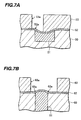
- FIGS. 7A and 7B are cross sectional views illustrating semiconductor device manufacturing methods according to third and fourth embodiments of the invention, respectively.
- an element separation insulating region 2 is formed to define active regions.
- the element separation insulating region 2 is formed by local oxidation of silicon (LOCOS), shallow trench isolation (STI) or the like.
- a MOSFET 3 is formed in the active region.
- MOSFET 3 has a gate electrode 3 G, a source region 3 S and a drain region 3 D.
- An interlayer insulating film 5 of silicon oxide (SiO 2 ) is formed on the silicon substrate 1 , covering MOSFET 3 .
- the interlayer insulating film 5 is formed by chemical vapor deposition (CVD).
- a plurality of via holes are formed through the interlayer insulating film 5 , and plugs made of tungsten (W) are filled in the via holes.
- Plugs 6 S and 6 D are connected to the source region 3 S and drain region 3 D, respectively.
- a barrier metal layer of TiN or the like is formed in the inner wall of each via hole.
- An etching stopper film 10 of SiN having a thickness of 30 nm is formed on the interlayer insulating film 5 .
- the etching stopper film 10 can be formed by plasma enhanced CVD.
- a wiring layer insulating film 11 of fluorosilicate glass (FSG) having a thickness of 500 nm is formed on the etching stopper film 10 .
- the wiring layer insulating film 11 can be formed by plasma CVD by using SiH 4 , SiF 4 , N 2 O and N 2 as source gasses.
- a resist film 12 is formed on the wiring layer insulating film 11 .
- an elongated opening 12 S passing above the plug 6 S and an elongated opening 12 D passing above the plug 6 D are formed through the resist film 12 .
- a width of the opening is about 0.25 ⁇ m and a width of the opening 12 D is about 0.5 ⁇ m.
- the wiring layer insulating film 11 is etched to form wiring grooves 11 S and 11 D corresponding to the openings 12 S and 12 D.
- the wiring layer insulating film 11 can be etched by reactive ion etching (RIE).
- RIE reactive ion etching
- an RIE system (UNITY 85-IEM) manufactured by Tokyo Electron Limited was used. The detailed etching conditions will be later described.
- the wider groove 11 D is etched faster than the narrower groove 11 S. Therefore, if the etching is stopped when the etching stopper film 10 is exposed on the bottom of the narrower groove 11 S, the upper layer of the etching stopper film 10 on the bottom of the wider groove 11 D is etched. After the wiring grooves 11 S and 11 D are formed, the resist film 12 is ashed and removed and thereafter, the etching stopper film 10 exposed on the bottoms of the grooves 11 S and 11 D is etched by using mixture gas of CHF 3 and O 2 .
- the inner walls of the wiring grooves 11 S and 11 D and the surface of the wiring layer insulating film 11 are covered with a barrier metal layer 15 made of Ta or the like.
- a barrier metal layer 15 made of Ta or the like.
- a seed layer of Cu is formed and a Cu film is filled in the wiring grooves 11 S and 11 D by plating. Unnecessary regions of the Cu film and barrier metal layer are removed by chemical mechanical polishing (CMP).
- CMP chemical mechanical polishing
- FIG. 4 is a schematic diagram showing the structure of an RIE system.
- a lower electrode 101 and an upper electrode 102 are disposed generally in parallel.
- Etching gas is introduced via a gas inlet port 109 into the chamber 100 , whereas unreacted etching gas and reaction byproducts are drained from an air outlet port 103 .
- a power source 106 applies a high frequency voltage of 27 MHz to the upper electrode 102 via an impedance matching circuit 107 .
- a bias power source 104 applies a high frequency voltage of 800 kHz to the lower electrode 101 via an impedance matching circuit 105 .
- a substrate 110 to be processed is placed on the lower electrode 101 .
- Etching gasses used were cyclic and saturated C 4 F 8 and chained and unsaturated C 5 F 8 , Ar, CO and O 2 at flow rates of 6 sccm, 4 sccm, 300 sccm, 100 sccm, and 10 sccm, respectively.
- a pressure in the chamber 100 was 5.3 Pa (40 mTorr)
- a source power supplied to the upper electrode 102 was 600 W
- a bias power supplied to the lower electrode 101 was 1400 W
- a temperature of the lower electrode 101 was 20° C.
- a ratio (selection ratio) of an etching rate of the FSG film to an etching rate of the SiN film was about 20.
- An etching rate of the narrower groove 11 S was about 400 nm/min and that of the wider groove 11 D was about 500 nm/min.
- an over-etch of 20% was performed. Namely, the etching time was set to a time of 90 seconds which forms the narrower groove 11 S having a depth of 600 nm at its etching rate (1.2 ⁇ 500 nm thickness of the wiring layer insulating film 11 ).
- An over-etch corresponding to a thickness of 100 nm (600 nm-500 nm) is therefore performed at the bottom of the narrower groove 11 S.
- This over-etch etches the etching stopper film 10 exposed on the bottom of the narrower groove 11 S by a depth of 5 nm (100 nm ⁇ fraction (1/20) ⁇ ).
- Etching the wider groove 11 D at its etching rate for 90 seconds corresponds to an etching amount of 750 nm. Since the thickness of the wiring layer insulating film 11 is 500 nm, an over-etch amount is 250 nm. This over-etch corresponds to an etch amount of 12.5 nm of the etching stopper film 10 exposed on the bottom of the wider groove 11 D, because the selection ratio of the FSG film to the SiN film is 20.
- the thickness of the etching stopper film 10 is 30 nm, an etching stopper film 10 having a sufficient thickness can be left also on the bottom of the wider groove 11 D. It is therefore possible to prevent the plugs 6 S and 6 D under the etching stopper film 10 from being etched.
- etching was performed without adding C 5 F 8 gas to the etching gasses.
- the etching gasses used were cyclic and saturated C 4 F 8 , Ar, CO and O 2 at the flow rates of 10 sccm, 200 sccm, 75 sccm and 6 sccm, respectively.
- a pressure in the chamber was 8 Pa (60 mTorr)
- a source power was 600 W
- a bias power was 1300 W
- a lower electrode temperature was 20° C.
- the etching selection ratio was 8. If the narrower groove 11 S is over-etched by 20% under these etching conditions, the etching stopper film 10 on the bottom of the wider groove 11 D is etched by about 31.3 nm. Since the thickness of the etching stopper film 10 is 30 nm, the plug 6 D is exposed on the bottom of the wider groove 11 D and the plug 6 D is partially etched.
- C 5 F 8 in the etching gasses increases the etching selection ratio. It is known that the etching selection ratio can be increased by adding CO gas. However, addition of CO gas only is insufficient, and if C 5 F 8 is added, the selection ratio can be increased further. O 2 gas has a function of improving clearance quality of etching. Ar gas is used for ion assistance.
- a Cu wiring 16 is buried in a wiring groove formed through a wiring layer insulating film 11 .
- the wiring layer insulating film 11 and its underlying structure are formed by a method similar to that of the first embodiment.
- Moisture proof rings 6 R and 16 R are formed slightly inside the outer periphery of a chip and along the chip outer periphery.
- the moisture proof ring 6 R is formed by the same process as the process of forming a tungsten plug 6
- the moisture proof ring 16 R is formed by the same process as the process of forming the Cu wiring 16 .
- An etching stopper film 20 of silicon nitride having a thickness of 50 nm is formed on the wiring layer insulating film 11 .
- the etching stopper film 20 is formed, for example, by plasma enhanced CVD and functions as a diffusion preventing and antioxidation film for the Cu wiring 16 .
- a via layer insulating film 21 of FSG having a thickness of 1000 nm is formed on this etching stopper film 20 .
- the via layer insulating film 21 is formed by plasma enhanced CVD.
- a resist film 22 is formed on the via layer insulating film 21 .
- An opening 22 H for forming a via hole and an opening 22 R for forming a moisture proof ring are formed through the resist film 22 .
- the opening 22 H is disposed superposing upon the Cu wiring 16 and the opening 22 R is disposed above the moisture proof ring 16 R and along this ring.
- the via layer insulating film 21 is etched. The detailed etching conditions will be later described. A via hole 21 H corresponding to the opening 22 H and a groove 21 R corresponding to the opening 22 R are therefore formed. The etching stopper film 20 is exposed on the bottoms of the via hole 21 H and groove 21 R.
- the resist film 22 is ashed and removed. At this time, since the upper surfaces of the Cu wiring 16 and moisture proof ring 16 R are covered with the etching stopper film 20 , it is possible to prevent oxidation of the Cu wiring 16 and moisture proof ring 16 R.
- organic material 30 is buried in the via hole 21 H and groove 21 R to set the depths of the hole and groove to 500 nm or shallower.
- the organic material 30 is resist from which photosensitive agent was removed.
- a resist film 31 is formed on the via layer insulating film 21 , the resist film 31 having openings overlapping the via hole 21 H and groove 21 R.
- the via layer insulating film 21 is etched. Since the etching stopper film 20 is protected by the organic material 30 , the etching stopper film 20 is not etched. The resist film 31 is thereafter ashed and removed. At this time, the organic material 30 is also removed.
- a wiring groove 32 continuous at its bottom with the via hole 21 H is therefore formed.
- the width of the upper portion of the groove 21 R is widened.
- the etching stopper film 20 exposed at the bottoms of the via hole 21 H and groove 21 R is etched by using mixture gas of CHF 3 and O 2 .
- the Cu wiring 16 and moisture proof ring 16 R are exposed at the bottoms of the via hole 21 H and groove 21 R. Similar to the method described with reference to FIG. 3, a barrier metal layer and a seed layer are formed, a Cu film is buried and then CMP is performed. A barrier metal layer 25 is therefore formed in the inner walls of the via hole 21 H and wiring groove 32 , and a Cu wiring 26 is buried in the via hole 21 H and wiring groove 32 . A barrier layer 25 R is also formed on the inner wall of the groove 21 R, and the inside of the groove 21 R is buried with a moisture proof ring 26 R of Cu.
- the copper wiring pattern is formed by the dual damascene method.
- a multi-layer wiring structure can be formed.
- Etching gasses used were cyclic and saturated C 4 F 8 and chained and unsaturated C 5 F 8 , Ar, Co and O 2 at flow rates of 8 sccm, 3 sccm, 320 sccm, 190 sccm, and 8 sccm, respectively.
- a pressure in the chamber 100 was 4 Pa (30 mTorr)
- a source power supplied to the upper electrode 102 was 1750 W
- a bias power supplied to the lower electrode 101 was 1400 W
- a temperature of the lower electrode 101 was 20° C.
- a ratio (selection ratio) of an etching rate of the FSG film to an etching rate of the SiN film was about 25.
- An etching rate of the via hole 21 H having a diameter of 0.3 ⁇ m was about 500 nm/min and that of the groove 21 R having a width of 0.3 ⁇ m was about 625 nm/min.
- an over-etch of 20% was performed in order to expose the etching stopper film 20 on the bottom of the via hole 21 H with good reproductivity. Namely, the etching time was set to a time of 144 seconds which forms the via hole 21 H having a depth of 1200 nm at its etching rate (1.2 ⁇ 1000 nm thickness of the via layer insulating film 21 ).
- An over-etch corresponding to a thickness of 200 nm (1200 nm-1000 nm) is therefore performed at the bottom of the via hole 21 H.
- This over-etch etches the etching stopper film 20 exposed on the bottom of the via hole 21 H by a depth of 8 nm (200 nm ⁇ fraction (1/25) ⁇ ).
- Etching the groove 21 R at its etching rate for 144 seconds corresponds to an etching amount of 1500 nm. Since the thickness of the wiring layer insulating film 11 is 1000 nm, an over-etch amount of the groove 21 R is 500 nm. This over-etch corresponds to an etch amount of 20 nm (500 nm ⁇ fraction (1/25) ⁇ ) of the etching stopper film 20 exposed on the bottom of the groove 21 R, because the selection ratio of the FSG film to the SiN film is 25.
- the thickness of the etching stopper film 20 is 50 nm, an etching stopper film 20 having a sufficient thickness can be left also on the bottom of the groove 21 R. It is therefore possible to prevent the Cu wiring 16 and moisture proof ring 16 R under the etching stopper film 20 from being exposed.
- an FSG film was etched without adding C 5 F 8 gas to the etching gasses.
- the etching gasses used were cyclic and saturated C 4 F 8 , Ar, CO and O 2 at the flow rates of 10 sccm, 200 sccm, 150 sccm and 6 sccm, respectively.
- a pressure in the chamber was 4 Pa (30 mTorr), a source power was 2000 W, a bias power was 1400 W, and a lower electrode temperature was 20° C.
- the etching selection ratio was 10. If the via hole 21 H is over-etched by 20% under these etching conditions, the etching stopper film 20 on the bottom of the groove 21 R is etched by about 50 nm. Since the thickness of the etching stopper film 20 is 50 nm, the moisture proof ring 16 R is exposed on the bottom of the groove 21 R. Therefore, the moisture proof ring 16 R is oxidized while the resist film 22 shown in FIG. 5A is ashed.
- the etching stopper film 20 is made thick to prevent exposure of the moisture proof ring 16 R.
- the etching stopper film 20 of SiN has a higher dielectric constant than the via layer insulating film 21 of FSG. If the etching stopper 20 is made thick, a parasitic capacitance between wirings is increased, which is undesirable.
- the etching selection ratio becomes high by adding chained and unsaturated C 5 F 8 gas to cyclic and saturated C 4 F 8 gas so that the etching stopper film can be made thin.
- the abscissa of the graph shown in FIG. 6 represents a ratio of a partial pressure of C 5 F 8 gas to a ratio of a sum of partial pressures of C 4 F 8 and C 5 F 8 gas in the unit of “%”, and the ordinate represents an etching rate of an FSG film in the unit of “ ⁇ m/min”.
- the partial pressure of C 5 F 8 gas is made large, the etching rate lowers.
- the etching selection ratio becomes high.
- the FSG film on the SiN film is etched.
- a high etching selection ratio is expected also when Si containing insulating films (other than an SiN film and SiON film) are etched.
- materials of such insulating films are silicon oxide (SiO 2 ), phosphosilicate glass (PSG), borosilicate glass (BSG), borophosphosilicate glass (BPSG), hydrogen silsesquioxane, tetraethylorthosilicate (TEOS), carbon containing silicon oxide (SiOC), spin-on-glass (SOG) and the like.
- chained and unsaturated C 5 F 8 gas is added to cyclic and saturated C 4 F 8 gas, and these gasses are used as etching gasses.
- Other fluorocarbon gas of a similar kind may also be used.
- chained and unsaturated C 4 F 8 gas may be used in place of cyclic and saturated C 4 F 8 gas.
- fluorocarbon gas expressed by a general formula C x F y (where x and y are an integer and satisfy x ⁇ 5 and y ⁇ (2x ⁇ 1)) may be used.
- C 4 F 6 gas may be used.
- the C 4 F 6 gas has a C/N ratio of 0.667 which is larger than the C/F ratio of 0.625 of the C 5 F 8 gas, and vapor phase polymerization of the C 4 F 6 gas is easier than the C 5 F 8 gas. Since this difference is small, the optimum addition amount of the C 4 F 6 gas to the C 4 F 8 gas is generally the same as that of the C 5 F 8 gas, although there is some difference between the amounts. Similar effects of adding the C 5 F 8 are expected.
- the etching method used by the above embodiments is applicable to manufacture of semiconductor devices of various structures, in addition to the embodiment structures.
- this etching method can be applied to a process of forming via holes at the same time above the source region, gate electrode and drain region.
- the embodiment etching method is also applicable to a process of forming via holes in a self alignment manner above the source and drain regions after the upper and side walls of the gate electrode are covered with an etching stopper film.
- the embodiment etching method is also applicable to a process of forming via holes and wiring grooves by a single damascene method.
- FIG. 7A is a cross sectional view showing a via hole formed through an insulating film by a semiconductor device manufacture method according to a third embodiment.
- a copper wiring 51 is buried in a surface layer of an underlying interlayer insulating film 50 .
- An etching stopper film 52 of SiN or SiC covers the surfaces of the copper wiring 51 and interlayer insulating film 50 .
- An insulating film 53 made of the same material as that of the wiring layer insulating film 11 of the first embodiment shown in FIG. 1 is formed on the etching stopper film 52 .
- a via hole 53 a is formed through the insulating film 53 .
- the via hole 53 a is formed by a method similar to the method of forming the via hole 21 H of the second embodiment shown in FIG. 5 A.
- the upper surface of the copper wiring 51 is usually depressed because of the characteristics inherent to CMP.
- the etching stopper film 52 is formed conformal to this depressed surface. If the via hole 53 a overlaps the edge of the copper wiring 51 because of an alignment position error, the projected area 52 a of the etching stopper film 52 is exposed on the bottom of the via hole 53 a . As the projected area 52 a of the etching stopper film 52 is exposed, an etching selection ratio usually lowers.
- the via hole 53 a is formed by the embodiment method, a high etching selection ratio can be obtained. Even if there is a position alignment error as shown in FIG. 7A, the etching can be stopped stably.
- FIG. 7B is a cross sectional view showing a wiring groove formed through an insulating film by a semiconductor device manufacture method according to a fourth embodiment.
- a plug 61 of copper or tungsten is disposed in a surface layer of an underlying interlayer insulating film 60 .
- An etching stopper film 62 of SiN or SiC is formed on the surfaces of the plug 61 and interlayer insulating film 60 .
- An insulating film 63 made of the same material as that of the wiring layer insulating film 11 of the first embodiment shown in FIG. 1 is formed on the etching stopper film 62 .
- a groove 63 a is formed through the insulating film 63 .
- the groove 63 a is formed by a method similar to the method of forming the wiring groove 11 S of the first embodiment shown in FIG. 2 .
- the upper surface of the plug 61 is usually projected. Therefore, a concave area 62 a is likely to be formed along the boarder between the plug 61 and interlayer insulating film 60 . If the wiring groove 63 a is formed by the embodiment method, a high etching selection ratio can be obtained. Even if there is the concave area 62 a as shown in FIG. 7B, the etching can therefore be stopped stably.
- RIE reactive ion etching
- ICP inductive coupled plasma
- ECR electron cyclotron resonance
Applications Claiming Priority (2)
| Application Number | Priority Date | Filing Date | Title |
|---|---|---|---|
| JP2001-300562 | 2001-09-28 | ||
| JP2001300562A JP4108310B2 (ja) | 2001-09-28 | 2001-09-28 | シリコン含有絶縁膜を有する半導体装置の製造方法 |
Publications (2)
| Publication Number | Publication Date |
|---|---|
| US20030064603A1 US20030064603A1 (en) | 2003-04-03 |
| US6787474B2 true US6787474B2 (en) | 2004-09-07 |
Family
ID=19121114
Family Applications (1)
| Application Number | Title | Priority Date | Filing Date |
|---|---|---|---|
| US10/040,378 Expired - Lifetime US6787474B2 (en) | 2001-09-28 | 2002-01-09 | Manufacture method for semiconductor device having silicon-containing insulating film |
Country Status (4)
| Country | Link |
|---|---|
| US (1) | US6787474B2 (zh) |
| JP (1) | JP4108310B2 (zh) |
| KR (1) | KR100698998B1 (zh) |
| TW (1) | TW517307B (zh) |
Cited By (3)
| Publication number | Priority date | Publication date | Assignee | Title |
|---|---|---|---|---|
| US6960535B1 (en) * | 2004-05-14 | 2005-11-01 | Sharp Kabushiki Kaisha | Dual damascene etching process |
| US20070179105A1 (en) * | 2006-01-31 | 2007-08-02 | Awdalla Essam T | Method and means for treating solid tumors |
| US20100003816A1 (en) * | 2005-02-04 | 2010-01-07 | Kabushiki Kaisha Toshiba | Method of manufacturing a semiconductor device from which damage layers and native oxide films in connection holes have been removed |
Families Citing this family (6)
| Publication number | Priority date | Publication date | Assignee | Title |
|---|---|---|---|---|
| US6861104B2 (en) * | 2002-05-22 | 2005-03-01 | United Microelectronics Corp. | Method of enhancing adhesion strength of BSG film to silicon nitride film |
| JP2005142369A (ja) * | 2003-11-06 | 2005-06-02 | Renesas Technology Corp | 半導体装置の製造方法 |
| US7794616B2 (en) * | 2004-08-09 | 2010-09-14 | Tokyo Electron Limited | Etching gas, etching method and etching gas evaluation method |
| US20100154874A1 (en) * | 2008-09-29 | 2010-06-24 | Takashi Hirose | Photoelectric conversion device and manufacturing method thereof |
| CN102437089B (zh) * | 2011-07-12 | 2014-05-28 | 上海华力微电子有限公司 | 一种铜后道互连工艺 |
| JP6937724B2 (ja) * | 2018-06-21 | 2021-09-22 | 三菱電機株式会社 | 半導体装置およびその製造方法 |
Citations (6)
| Publication number | Priority date | Publication date | Assignee | Title |
|---|---|---|---|---|
| JPH022000A (ja) | 1988-06-13 | 1990-01-08 | Fuji Xerox Co Ltd | 電子装置筐体の電磁波遮蔽構造 |
| JPH0338950A (ja) | 1989-07-05 | 1991-02-20 | Canon Inc | 通信装置 |
| US5338399A (en) * | 1991-02-12 | 1994-08-16 | Sony Corporation | Dry etching method |
| US5503901A (en) * | 1993-06-30 | 1996-04-02 | Kabushiki Kaisha Toshiba | Surface treatment method and surface treatment apparatus |
| JP2001110790A (ja) | 1999-08-02 | 2001-04-20 | Matsushita Electronics Industry Corp | プラズマ処理方法 |
| US6380096B2 (en) * | 1998-07-09 | 2002-04-30 | Applied Materials, Inc. | In-situ integrated oxide etch process particularly useful for copper dual damascene |
Family Cites Families (1)
| Publication number | Priority date | Publication date | Assignee | Title |
|---|---|---|---|---|
| JP4216922B2 (ja) * | 1998-05-08 | 2009-01-28 | 東京エレクトロン株式会社 | 酸化膜のエッチング方法 |
-
2001
- 2001-09-28 JP JP2001300562A patent/JP4108310B2/ja not_active Expired - Fee Related
- 2001-12-31 TW TW090133370A patent/TW517307B/zh not_active IP Right Cessation
-
2002
- 2002-01-09 US US10/040,378 patent/US6787474B2/en not_active Expired - Lifetime
- 2002-02-28 KR KR1020020010870A patent/KR100698998B1/ko not_active IP Right Cessation
Patent Citations (6)
| Publication number | Priority date | Publication date | Assignee | Title |
|---|---|---|---|---|
| JPH022000A (ja) | 1988-06-13 | 1990-01-08 | Fuji Xerox Co Ltd | 電子装置筐体の電磁波遮蔽構造 |
| JPH0338950A (ja) | 1989-07-05 | 1991-02-20 | Canon Inc | 通信装置 |
| US5338399A (en) * | 1991-02-12 | 1994-08-16 | Sony Corporation | Dry etching method |
| US5503901A (en) * | 1993-06-30 | 1996-04-02 | Kabushiki Kaisha Toshiba | Surface treatment method and surface treatment apparatus |
| US6380096B2 (en) * | 1998-07-09 | 2002-04-30 | Applied Materials, Inc. | In-situ integrated oxide etch process particularly useful for copper dual damascene |
| JP2001110790A (ja) | 1999-08-02 | 2001-04-20 | Matsushita Electronics Industry Corp | プラズマ処理方法 |
Cited By (5)
| Publication number | Priority date | Publication date | Assignee | Title |
|---|---|---|---|---|
| US6960535B1 (en) * | 2004-05-14 | 2005-11-01 | Sharp Kabushiki Kaisha | Dual damascene etching process |
| US20050255703A1 (en) * | 2004-05-14 | 2005-11-17 | Masayuki Sato | Dual damascene etching process |
| US20100003816A1 (en) * | 2005-02-04 | 2010-01-07 | Kabushiki Kaisha Toshiba | Method of manufacturing a semiconductor device from which damage layers and native oxide films in connection holes have been removed |
| US8232197B2 (en) * | 2005-02-04 | 2012-07-31 | Kabushiki Kaisha Toshiba | Method of manufacturing a semiconductor device from which damage layers and native oxide films in connection holes have been removed |
| US20070179105A1 (en) * | 2006-01-31 | 2007-08-02 | Awdalla Essam T | Method and means for treating solid tumors |
Also Published As
| Publication number | Publication date |
|---|---|
| US20030064603A1 (en) | 2003-04-03 |
| JP4108310B2 (ja) | 2008-06-25 |
| JP2003109940A (ja) | 2003-04-11 |
| KR20030026809A (ko) | 2003-04-03 |
| TW517307B (en) | 2003-01-11 |
| KR100698998B1 (ko) | 2007-03-26 |
Similar Documents
| Publication | Publication Date | Title |
|---|---|---|
| US20030068582A1 (en) | Method of manufacturing semiconductor device having silicon carbide film | |
| US6849539B2 (en) | Semiconductor device and method of fabricating the same | |
| US6815823B2 (en) | Copper metal structure for the reduction of intra-metal capacitance | |
| US5866920A (en) | Semiconductor device and manufacturing method of the same | |
| US6939798B2 (en) | Method for forming T-shaped conductor wires of semiconductor device | |
| US6337282B2 (en) | Method for forming a dielectric layer | |
| JP4368058B2 (ja) | 反射防止エッチストップ層を含む半導体装置を製造するためのプロセス | |
| US6599830B2 (en) | Semiconductor device and manufacturing method thereof | |
| US6140224A (en) | Method of forming a tungsten plug | |
| US6309955B1 (en) | Method for using a CVD organic barc as a hard mask during via etch | |
| US20080207000A1 (en) | Method of making high-aspect ratio contact hole | |
| JP2002043419A (ja) | 半導体装置の製造方法及び半導体装置 | |
| US6232237B1 (en) | Method for fabricating semiconductor device | |
| US6506680B1 (en) | Method of forming connections with low dielectric insulating layers | |
| US6787474B2 (en) | Manufacture method for semiconductor device having silicon-containing insulating film | |
| US5880030A (en) | Unlanded via structure and method for making same | |
| US20090137119A1 (en) | Novel seal isolation liner for use in contact hole formation | |
| US6492276B1 (en) | Hard masking method for forming residue free oxygen containing plasma etched layer | |
| KR100438630B1 (ko) | 반도체 장치의 제조방법 | |
| KR100522761B1 (ko) | 쌍상감법을 이용한 반도체 메모리 소자의 패턴 형성 방법 | |
| JP3317279B2 (ja) | 半導体装置の製造方法 | |
| KR100236052B1 (ko) | 반도체장치의 다층배선 형성방법 | |
| KR100451492B1 (ko) | 반도체소자의콘택홀형성방법 | |
| KR100279246B1 (ko) | 반도체 소자의 텅스텐 플러그 형성방법 | |
| KR20050045375A (ko) | 듀얼 다마신 패턴 형성 방법 |
Legal Events
| Date | Code | Title | Description |
|---|---|---|---|
| AS | Assignment |
Owner name: FUJITSU LIMITED, JAPAN Free format text: ASSIGNMENT OF ASSIGNORS INTEREST;ASSIGNOR:KOMADA, DAISUKE;REEL/FRAME:012473/0683 Effective date: 20011218 |
|
| AS | Assignment |
Owner name: FUJITSU LIMITED, JAPAN Free format text: CORRECTIVE ASSIGNMENT TO CORRECT THE ASSIGNEE'S ADDRESS PREVIOUSLY RECORDED ON REEL 012473, FRAME 0683;ASSIGNOR:KOMADA, DAISUKE;REEL/FRAME:012856/0687 Effective date: 20011218 |
|
| STCF | Information on status: patent grant |
Free format text: PATENTED CASE |
|
| FPAY | Fee payment |
Year of fee payment: 4 |
|
| AS | Assignment |
Owner name: FUJITSU MICROELECTRONICS LIMITED, JAPAN Free format text: ASSIGNMENT OF ASSIGNORS INTEREST;ASSIGNOR:FUJITSU LIMITED;REEL/FRAME:021998/0645 Effective date: 20081104 Owner name: FUJITSU MICROELECTRONICS LIMITED,JAPAN Free format text: ASSIGNMENT OF ASSIGNORS INTEREST;ASSIGNOR:FUJITSU LIMITED;REEL/FRAME:021998/0645 Effective date: 20081104 |
|
| AS | Assignment |
Owner name: FUJITSU SEMICONDUCTOR LIMITED, JAPAN Free format text: CHANGE OF NAME;ASSIGNOR:FUJITSU MICROELECTRONICS LIMITED;REEL/FRAME:024982/0245 Effective date: 20100401 |
|
| FPAY | Fee payment |
Year of fee payment: 8 |
|
| FPAY | Fee payment |
Year of fee payment: 12 |
|
| AS | Assignment |
Owner name: FUJITSU SEMICONDUCTOR LIMITED, JAPAN Free format text: CHANGE OF ADDRESS;ASSIGNOR:FUJITSU SEMICONDUCTOR LIMITED;REEL/FRAME:041188/0401 Effective date: 20160909 |