US6469386B1 - Lead frame and method for plating the same - Google Patents
Lead frame and method for plating the same Download PDFInfo
- Publication number
- US6469386B1 US6469386B1 US09/492,402 US49240200A US6469386B1 US 6469386 B1 US6469386 B1 US 6469386B1 US 49240200 A US49240200 A US 49240200A US 6469386 B1 US6469386 B1 US 6469386B1
- Authority
- US
- United States
- Prior art keywords
- lead frame
- layer
- plated
- alloy
- intermediate layer
- Prior art date
- Legal status (The legal status is an assumption and is not a legal conclusion. Google has not performed a legal analysis and makes no representation as to the accuracy of the status listed.)
- Expired - Lifetime
Links
Images


Classifications
-
- C—CHEMISTRY; METALLURGY
- C23—COATING METALLIC MATERIAL; COATING MATERIAL WITH METALLIC MATERIAL; CHEMICAL SURFACE TREATMENT; DIFFUSION TREATMENT OF METALLIC MATERIAL; COATING BY VACUUM EVAPORATION, BY SPUTTERING, BY ION IMPLANTATION OR BY CHEMICAL VAPOUR DEPOSITION, IN GENERAL; INHIBITING CORROSION OF METALLIC MATERIAL OR INCRUSTATION IN GENERAL
- C23C—COATING METALLIC MATERIAL; COATING MATERIAL WITH METALLIC MATERIAL; SURFACE TREATMENT OF METALLIC MATERIAL BY DIFFUSION INTO THE SURFACE, BY CHEMICAL CONVERSION OR SUBSTITUTION; COATING BY VACUUM EVAPORATION, BY SPUTTERING, BY ION IMPLANTATION OR BY CHEMICAL VAPOUR DEPOSITION, IN GENERAL
- C23C28/00—Coating for obtaining at least two superposed coatings either by methods not provided for in a single one of groups C23C2/00 - C23C26/00 or by combinations of methods provided for in subclasses C23C and C25C or C25D
- C23C28/02—Coating for obtaining at least two superposed coatings either by methods not provided for in a single one of groups C23C2/00 - C23C26/00 or by combinations of methods provided for in subclasses C23C and C25C or C25D only coatings only including layers of metallic material
- C23C28/021—Coating for obtaining at least two superposed coatings either by methods not provided for in a single one of groups C23C2/00 - C23C26/00 or by combinations of methods provided for in subclasses C23C and C25C or C25D only coatings only including layers of metallic material including at least one metal alloy layer
-
- C—CHEMISTRY; METALLURGY
- C23—COATING METALLIC MATERIAL; COATING MATERIAL WITH METALLIC MATERIAL; CHEMICAL SURFACE TREATMENT; DIFFUSION TREATMENT OF METALLIC MATERIAL; COATING BY VACUUM EVAPORATION, BY SPUTTERING, BY ION IMPLANTATION OR BY CHEMICAL VAPOUR DEPOSITION, IN GENERAL; INHIBITING CORROSION OF METALLIC MATERIAL OR INCRUSTATION IN GENERAL
- C23C—COATING METALLIC MATERIAL; COATING MATERIAL WITH METALLIC MATERIAL; SURFACE TREATMENT OF METALLIC MATERIAL BY DIFFUSION INTO THE SURFACE, BY CHEMICAL CONVERSION OR SUBSTITUTION; COATING BY VACUUM EVAPORATION, BY SPUTTERING, BY ION IMPLANTATION OR BY CHEMICAL VAPOUR DEPOSITION, IN GENERAL
- C23C28/00—Coating for obtaining at least two superposed coatings either by methods not provided for in a single one of groups C23C2/00 - C23C26/00 or by combinations of methods provided for in subclasses C23C and C25C or C25D
- C23C28/02—Coating for obtaining at least two superposed coatings either by methods not provided for in a single one of groups C23C2/00 - C23C26/00 or by combinations of methods provided for in subclasses C23C and C25C or C25D only coatings only including layers of metallic material
- C23C28/023—Coating for obtaining at least two superposed coatings either by methods not provided for in a single one of groups C23C2/00 - C23C26/00 or by combinations of methods provided for in subclasses C23C and C25C or C25D only coatings only including layers of metallic material only coatings of metal elements only
-
- C—CHEMISTRY; METALLURGY
- C23—COATING METALLIC MATERIAL; COATING MATERIAL WITH METALLIC MATERIAL; CHEMICAL SURFACE TREATMENT; DIFFUSION TREATMENT OF METALLIC MATERIAL; COATING BY VACUUM EVAPORATION, BY SPUTTERING, BY ION IMPLANTATION OR BY CHEMICAL VAPOUR DEPOSITION, IN GENERAL; INHIBITING CORROSION OF METALLIC MATERIAL OR INCRUSTATION IN GENERAL
- C23C—COATING METALLIC MATERIAL; COATING MATERIAL WITH METALLIC MATERIAL; SURFACE TREATMENT OF METALLIC MATERIAL BY DIFFUSION INTO THE SURFACE, BY CHEMICAL CONVERSION OR SUBSTITUTION; COATING BY VACUUM EVAPORATION, BY SPUTTERING, BY ION IMPLANTATION OR BY CHEMICAL VAPOUR DEPOSITION, IN GENERAL
- C23C28/00—Coating for obtaining at least two superposed coatings either by methods not provided for in a single one of groups C23C2/00 - C23C26/00 or by combinations of methods provided for in subclasses C23C and C25C or C25D
- C23C28/02—Coating for obtaining at least two superposed coatings either by methods not provided for in a single one of groups C23C2/00 - C23C26/00 or by combinations of methods provided for in subclasses C23C and C25C or C25D only coatings only including layers of metallic material
- C23C28/027—Coating for obtaining at least two superposed coatings either by methods not provided for in a single one of groups C23C2/00 - C23C26/00 or by combinations of methods provided for in subclasses C23C and C25C or C25D only coatings only including layers of metallic material including at least one metal matrix material comprising a mixture of at least two metals or metal phases or metal matrix composites, e.g. metal matrix with embedded inorganic hard particles, CERMET, MMC.
-
- H—ELECTRICITY
- H10—SEMICONDUCTOR DEVICES; ELECTRIC SOLID-STATE DEVICES NOT OTHERWISE PROVIDED FOR
- H10W—GENERIC PACKAGES, INTERCONNECTIONS, CONNECTORS OR OTHER CONSTRUCTIONAL DETAILS OF DEVICES COVERED BY CLASS H10
- H10W70/00—Package substrates; Interposers; Redistribution layers [RDL]
- H10W70/40—Leadframes
- H10W70/456—Materials
- H10W70/457—Materials of metallic layers on leadframes
-
- H—ELECTRICITY
- H10—SEMICONDUCTOR DEVICES; ELECTRIC SOLID-STATE DEVICES NOT OTHERWISE PROVIDED FOR
- H10W—GENERIC PACKAGES, INTERCONNECTIONS, CONNECTORS OR OTHER CONSTRUCTIONAL DETAILS OF DEVICES COVERED BY CLASS H10
- H10W72/00—Interconnections or connectors in packages
- H10W72/071—Connecting or disconnecting
- H10W72/075—Connecting or disconnecting of bond wires
-
- H—ELECTRICITY
- H10—SEMICONDUCTOR DEVICES; ELECTRIC SOLID-STATE DEVICES NOT OTHERWISE PROVIDED FOR
- H10W—GENERIC PACKAGES, INTERCONNECTIONS, CONNECTORS OR OTHER CONSTRUCTIONAL DETAILS OF DEVICES COVERED BY CLASS H10
- H10W72/00—Interconnections or connectors in packages
- H10W72/50—Bond wires
- H10W72/541—Dispositions of bond wires
- H10W72/5449—Dispositions of bond wires not being orthogonal to a side surface of the chip, e.g. fan-out arrangements
-
- H—ELECTRICITY
- H10—SEMICONDUCTOR DEVICES; ELECTRIC SOLID-STATE DEVICES NOT OTHERWISE PROVIDED FOR
- H10W—GENERIC PACKAGES, INTERCONNECTIONS, CONNECTORS OR OTHER CONSTRUCTIONAL DETAILS OF DEVICES COVERED BY CLASS H10
- H10W72/00—Interconnections or connectors in packages
- H10W72/50—Bond wires
- H10W72/551—Materials of bond wires
- H10W72/552—Materials of bond wires comprising metals or metalloids, e.g. silver
- H10W72/5522—Materials of bond wires comprising metals or metalloids, e.g. silver comprising gold [Au]
-
- H—ELECTRICITY
- H10—SEMICONDUCTOR DEVICES; ELECTRIC SOLID-STATE DEVICES NOT OTHERWISE PROVIDED FOR
- H10W—GENERIC PACKAGES, INTERCONNECTIONS, CONNECTORS OR OTHER CONSTRUCTIONAL DETAILS OF DEVICES COVERED BY CLASS H10
- H10W72/00—Interconnections or connectors in packages
- H10W72/50—Bond wires
- H10W72/59—Bond pads specially adapted therefor
-
- H—ELECTRICITY
- H10—SEMICONDUCTOR DEVICES; ELECTRIC SOLID-STATE DEVICES NOT OTHERWISE PROVIDED FOR
- H10W—GENERIC PACKAGES, INTERCONNECTIONS, CONNECTORS OR OTHER CONSTRUCTIONAL DETAILS OF DEVICES COVERED BY CLASS H10
- H10W72/00—Interconnections or connectors in packages
- H10W72/90—Bond pads, in general
- H10W72/951—Materials of bond pads
- H10W72/952—Materials of bond pads comprising metals or metalloids, e.g. PbSn, Ag or Cu
-
- H—ELECTRICITY
- H10—SEMICONDUCTOR DEVICES; ELECTRIC SOLID-STATE DEVICES NOT OTHERWISE PROVIDED FOR
- H10W—GENERIC PACKAGES, INTERCONNECTIONS, CONNECTORS OR OTHER CONSTRUCTIONAL DETAILS OF DEVICES COVERED BY CLASS H10
- H10W74/00—Encapsulations, e.g. protective coatings
-
- H—ELECTRICITY
- H10—SEMICONDUCTOR DEVICES; ELECTRIC SOLID-STATE DEVICES NOT OTHERWISE PROVIDED FOR
- H10W—GENERIC PACKAGES, INTERCONNECTIONS, CONNECTORS OR OTHER CONSTRUCTIONAL DETAILS OF DEVICES COVERED BY CLASS H10
- H10W90/00—Package configurations
- H10W90/701—Package configurations characterised by the relative positions of pads or connectors relative to package parts
- H10W90/751—Package configurations characterised by the relative positions of pads or connectors relative to package parts of bond wires
- H10W90/756—Package configurations characterised by the relative positions of pads or connectors relative to package parts of bond wires between a chip and a stacked lead frame, conducting package substrate or heat sink
Definitions
- the present invention relates to a lead frame for semiconductor packages and a method for plating the lead frame, and more particularly, to a pre-plated lead frame having an improved outermost plated layer over a metal substrate and a method for plating the lead frame.
- Lead frames which form a semiconductor package together with a semiconductor chip, serve to support the semiconductor chip in the package in addition to electrically connecting the chip to an external circuit.
- FIG. 1 An example of a lead frame is shown in FIG. 1 .
- the lead frame 10 includes a pad 11 , an inner lead 12 and an outer lead 13
- the lead frame 10 is usually manufactured by stamping or etching.
- FIG. 2 shows an example of a semiconductor package.
- a semiconductor chip 15 which is mounted on the pad 11 , is connected to the inner lead 12 by wire bonding.
- the outer lead 13 is electrically connected to an external circuit.
- the chip 15 and the inner lead 12 are molded with a resin 14 , so that a semiconductor package 16 is completed.
- edges of the pad 11 and inner lead 12 are plated with a metal such as silver (Ag) so as to improve the wire bonding properties between the chip 15 and the inner lead 12 , and the characteristics of the pad 11 .
- a metal such as silver (Ag)
- solder containing tin (Sn) and lead (Pb) is deposited on a predetermined area of the outer lead 12 .
- the plating and the soldering are carried out by wet processes after the molding with resin, so that the reliability problem rises.
- a pre-plated frame has been suggested.
- plated layers are formed with a material having good solder wettability on a lead frame.
- FIG. 3 shows an example of a lead frames manufactured by the conventional pre-plating technique.
- the Ni plated layer 22 prevents diffusion of Cu or Fe of the metal substrate 21 up to the surface of the lead frame, by which copper oxide or copper sulfide are produced on the frame surface.
- the Pd outermost plated layer 23 is formed of a good solderability material to provide a protective function for the surface of the nickel plate layer 22 .
- Ni plating for the Ni plated layer proceeds faster in the defect region than in the other region, resulting in a rough surface of the plated layer due to a decreased coherence with the other region.
- Pd is plated on the surface of the Ni plated layer formed on the defect region by electroplating, a large amount of hydrogen bubbles effervescing in electrolyte, are incorporated into the Pd plated layer during the plating with Pd. This is because the Pd deposition potential is similar to the hydrogen deposition potential.
- FIG. 4 Another example of a lead frame manufactured by the pre-plating technique, which has been suggested so as to solve the above problems, is shown in FIG. 4 .
- the lead frame 20 ′ shown in FIG. 4 further comprises a thin film 24 formed of gold (Au) on the Pd plated layer 23 compared to the lead frame 20 in FIG. 2 .
- Au gold
- Au having good oxidation resistance is used to plate the Pd plated layer so as to prevent oxidation of the Pd plated layer 23 with an improved solderability.
- the plating of Au on the Pd plated layer is for preventing the oxidation of the Pd plated layer by the thermal process for semiconductor manufacture, thereby improving the solderability in mounting the completed package onto a PCB.
- the topography of the Au plated layer is an important concern for improving the Au plating effects.
- a known Au plating technique is not sufficient to provide an even plated layer on the Pd plated layer.
- the Au plated layer is usually formed to a thickness of 0.3 microinch so as to prevent the oxidation of Pd.
- the Au plate layer which is formed as an anti-oxidation layer for Pd, relatively decreases the adhesion of a chip to a die.
- the Au plated layer can improve the solder wettiablity during soldering compared to a conventional lead frame.
- the Au plated layer is easy to be broken by external impacts after being mounted on a PCB.
- the localized plating i.e., plating only the outer lead portion.
- the localized plating requires additional masks for the plating, which raises the manufacturing costs and lowers productivity. Due to this reason, the Au plate layer has been formed over the intermediate palladium plate layer so as to prevent the oxidation of the palladium plate layer, despite its costs.
- U.S. Pat. No. 5,767,574 teaches a lead frame capable of eliminating the above problems, which includes a Ni alloy plated layer, a Pd strike plated layer and a Pd alloy layer which are sequentially formed on a metal substrate.
- the outermost Pd alloy plated layer is composed of Pd and Au.
- the problem of the oxidation of Pd and the high cost of using Au can be eliminated by the outermost plated layer including Au.
- the restricted use of Au in the outermost layer improves the adhesion with resin in semiconductor packaging and minimizes the possibility of being broken after mounted on a PCB.
- plating Au in the Pd-based outermost plate layer it is difficult to effectively prevent the incorporation of hydrogen bubbles into the outermost layer.
- the above object is achieved by the method according to the present invention for manufacturing a lead frame, the method comprising: forming a protective layer with nickel (Ni) or Ni alloy on a metal substrate; forming an intermediate layer with palladium (Pd) or Pd alloy on the protective layer; and alternately plating the surface of the intermediate layer with Pd and gold (Au) at least one time to form an outermost layer including both Pd and Au particles.
- the alternate plating to form the outermost layer either Pd or Au can be plated first on the intermediated layer.
- first Pd is roughly plated at the nucleation site of the intermediate layer by applying the pulse current, and in turn Au is accumulated filling the space between accumulated Pd particles. Because the Au deposition potential is lower than that the Pd deposition potential, Au particles can be easily accumulated between the Pd particles.
- a lead frame for a semiconductor package comprising: a protective layer formed of nickel (Ni) or Ni alloy on a metal substrate; an intermediate layer formed of palladium (Pd) on the protective layer; and an outermost layer formed of Pd and gold (Au) on the Pd intermediate layer.
- the present invention provides a lead frame for a semiconductor package, comprising: a protective layer formed of nickel (Ni) or Ni alloy on a metal substrate; and an outermost layer formed of palladium (Pd) and gold (Au) on the protective layer.
- FIG. 1 is a plan view of a general lead frame
- FIG. 2 is an exploded perspective view of a semiconductor package
- FIGS. 3 and 4 are sectional views depicting examples of a conventional lead frame
- FIG. 5 is a sectional view of an embodiment of a lead frame according to the present invention.
- FIG. 6 is a sectional view of another embodiment of the lead frame according to the present invention.
- FIG. 7 is a sectional view of another embodiment of the lead frame according to the present invention.
- FIG. 8 is a partially enlarged perspective view of the lead frame in FIG. 7;
- FIGS. 9A through 9C are sectional views illustrating lead frame manufacture according to the present invention.
- FIG. 10 is a graph showing the adhesion with resins for a lead frame according to the present invention and for Comparative Examples.
- FIG. 11 is a graph showing the solderability of a lead frame according to the present invention and Comparative Examples.
- the lead frame includes a metal substrate 31 formed of copper (Cu), Cu alloy or iron-nickel (Fe—Ni) alloy, a protective layer 32 formed of Ni or Ni alloy on the metal substrate 31 , an intermediate layer 33 formed of palladium (Pd) or Pd alloy on the protective layer 32 , and an outermost layer 34 , which includes Pd and gold (Au) particles, formed on the intermediate layer 32 .
- the outermost layer 34 may be formed by plating alternately with Pd and Au.
- FIG. 6 Another example of the lead frame according to the present invention is shown in FIG. 6 .
- the lead frame 40 in FIG. 6 includes a protective layer 42 formed of Ni or Ni alloy and an outermost layer 43 , which are sequentially stacked on a metal substrate 41 .
- the outermost layer 43 both Pd and Au particles are present as in the lead frame shown in FIG. 5 .
- the metal of the outermost layer is not limited to Pd and Au.
- silver (Ag) may be used instead of Au.
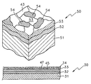
- FIG. 7 shows another example of the lead frame according to the present invention.
- the lead frame 50 has a protective layer 52 formed of Ni or Ni alloy on a metal substrate 51 .
- An intermediate layer 53 is formed of Pd or Pd alloy on the protective layer 52 .
- Plated regions 54 having a small thickness are locally formed over the intermediate layer 53 with Au or Au alloy.
- the location of the plated regions 54 on the intermediate layer 53 can be seen in FIG. 8 .
- the thickness of the plated regions is equivalent to the height of several atoms.
- the intermediate layer 53 is locally exposed or occupied by the plated regions 54 .
- the Au alloy for the plated regions 54 is Au-Pd or Au-Ag.
- FIGS. 9A through 9C illustrate an embodiment of lead frame manufacture according to the present invention.
- the metal substrate 31 formed of Cu, Cu alloy or Fe alloy is prepared, and the protective layer 32 is formed of Ni or Ni alloy on the metal substrate as shown in FIG. 9 A.
- the intermediate layer 33 is formed of Pd or Pd alloy on the protective layer 32 as shown in FIG. 9 B.
- the protective layer 32 and the intermediate layer 33 can be plated by applying pulse current, or by sputtering or vacuum deposition.
- the outermost layer 34 where Pd and Au particles 47 coexist is formed on the intermediate layer 33 , completing the lead frame (see FIG. 9 C).
- the outermost layer 34 is formed by the plating with application of pulse current. In other words, palladium is accumulated only at nucleation sites on the protective layer 32 by adjusting current density and plating time, resulting in palladium spots 45 on the surface of the intermediate layer 33 .
- Au is accumulated filling the space between deposited Pd particles on the intermediate layer 33 .
- the Au deposition potential which is lower than the Pd deposition potential allows easy electroplating of Au between Pd particles.
- Pd is accumulated again to fill porosities or micro cracks which may present between the Au and Pd particles and cause unstable lead frame, resulting in the outermost layer 34 on the intermediate layer 33 .
- the plated “regions” 54 that are scattered on the intermediate layer 53 can be formed by plating with Au or Au alloy.
- the outermost layer 34 of the lead frame according to the present invention can be formed by alternately accumulating Pd and Au by plating.
- a pulse current is applied.
- the rectangular waveform of the pulse current may be a series of positive pulses separated by a predetermined interval.
- the waveform of the current may also alternate between positive and negative pulses. There may also be a predetermined interval between the positive and negative pulses.
- the waveform of the current may alternate between positive and negative pulses, wherein each of the positive and negative pulses are modulated by a small pulse train.
- the lead frame 50 as shown in FIG. 8 is formed by high pulse application so as to improve evenness of the intermediate layer 53 made of Pd or Pd alloy. Also, the formation of the plated regions 54 with Au or Au alloy on the surface of the intermediate layer 53 can be achieved by the high-pulse application, sputtering or deposition.
- the outermost layer 34 on the intermediate layer 33 or the surface of the intermediate layer 53 having the plated regions 54 includes both Pd and Au particles having good wire bonding properties. Also, the presence of Au decreases the area of the outermost layer occupied by Pd that is subjected to oxidation. Accordingly, the conventional problems can be eliminated. In addition, since the oxidation of Pd occurs after the wire bonding, the adhesion of the outermost layer 34 with mold resin is improved. Also, the alternated plating with Pd and Au allows the intermediate layer 33 having an improved protective function, by eliminating perforations due to hydrogen bubbles. Also, the interaction between Pd and Au in the outermost layer 34 improves the solderability and wire bonding properties compared to the case of forming the outermost layer exclusively including Au. Furthermore, since the Au or Au alloy layer is formed as thin as possible, the amount of expensive Au used can be reduced, lowering the manufacturing cost.
- a Pd intermediate layer was formed to have a thickness of 0.2 microinch and an outermost layer including both Pd and Au particles was formed on the Pd intermediate layer. Also, a lead frame having a Au outermost layer on the Pd intermediate layer was manufactured for Comparative Example 1, a lead frame having no outermost layer on the Pd plated layer was manufactured for Comparative Example 2, a lead frame having a Pd—Au plated layer on the Pd intermediate layer was manufactured for Comparative Example 3.
- the lead frame was baked at 250° C. for 5 minutes and cured at 270° C. for 1 hour. After bending leads of the frame, the lead frame was exposed to curing at 175° C. for 1 hour, and in turn steam aging at 95° C. for 8 hours.
- a wire bonding test a Au wire having a diameter of 1 mil was used. The bonding power and bonding force applied at the chip mounted on the pad and at the inner lead were 90 mW and 100 mN. The bonding period of time was 15 msec and 20 msec with respect to the chip on the pad and the inner lead, respectively. Then, the tension force of the Au wire bonded across the chip and the inner lead was measured.
- Table 1 shows that both the solderability and wire bonding strength are improved for the lead frame according to the present invention.
- a Pd intermediate layer was formed to have a thickness of 0.2 microinch and an outermost layer including both Pd and Au particles was formed on the Pd intermediate layer 0.2-microinch thick. Also, a lead frame having a Au outermost layer on a Pd intermediate layer having a thickness of 0.8 microinch was manufactured for Comparative Example 1, and a lead frame having no outermost layer on a Pd plated layer having a thickness of 0.2 microinch was manufactured for Comparative Example 2.
- the lead frame was baked at 360° C. for 1 minutes.
- a Au wire having a diameter of 1 mil was used for a solderability test.
- the bonding power and bonding force applied at the chip mounted on the pad and at the inner lead were 90 mW and 100 mN.
- the bonding period of time was 15 msec and 20 msec with respect to the chip on the pad and the inner lead, respectively. Then, the tension force of the Au wire bonded across the chip and the inner lead was measured.
- Example 1 Present Invention Number of layers 3L 2L 2.5L Solderability (%) 85-95 60-80 100 Minimum wire 2.65 0.91 7.03 bonding strength (gf) Maximum wire 7.58 6.86 9.64 bonding strength (gf) Average wire 4.73 3.55 8.81 bonding strength (gf)
- the adhesion between the outermost layer and resin was measured for the lead frames manufactured in Example 1.
- two commercially available thermocurable resins (SL7300 and T16BC) were used to mold the lead frame. The result is shown in FIG. 10 .
- the adhesion force between the outermost layer and rein is maximum with respect to the lead frame having the Pd—Au outermost layer on the Pd intermediate layer for both two resins.
- a Ni protective layer was formed on a metal substrate formed of Cu to have a thickness of 30 microinch, and a Pd intermediate layer was formed on the Ni protective layer to have a thickness of 0.8 microinch.
- plated regions formed of Au or Au alloy were formed being scattered on the Pd intermediate layer to have a thickness of about 0.03 microinch.
- Comparative Example 1 0.3 microinch-thick plate regions were formed of Au or Au alloy on a general PPF lead frame.
- the lead frame was cured at 275° C. for 1 hours in an oven. After bending leads of the frame, the lead frame was exposed to curing at 175° C. for 2 hours, and in turn steam aging at 95° C. for 8 hours.
- a wire bonding test a Au wire having a diameter of 1 mil was used.
- the bonding power and bonding force applied at the chip mounted on the pad and at the inner lead of the frame were 90 mW and 100 mN.
- the bonding period of time was 15 msec and 20 msec with respect to the chip on the pad and the inner lead, respectively, and the bonding temperature was 215° C. Then, the tension force of the Au wire bonded across the chip and the inner lead was measured.
- the outer lead of the frame was immersed in an R flux at 245° C. for 5 seconds and drawn out of the flux, and an area of the outer lead with the flux with respect to the total area of the outer lead is shown by percentage.
- the hatching bars represent the result of the solderability test, and the plot represents the result of the wire bonding test.
- the solderability and the wire bonding strength for Comparative Example 1 are 60% and 2.69 gf, respectively.
- the solderability and the wire bonding strength for Comparative Example 2 are 80% and 2.69 gf, respectively.
- those for the lead frame according to the present invention are improved at 100% and 5.91 gf, respectively.
- the wire bonding strength of a lead frame according to the present invention was measured with a reduced bonding power and bonding force.
- a lead frame having plated portions on a Pd intermediate layer having a thickness of 1.0 microinch was manufactured.
- a lead frame having a 1.2 microinch Pd layer as an outermost layer was manufactured.
- a wire bonding test a capillary having a diameter of 80 micrometer, and a Au wire having a diameter of 0.8 mil were used.
- the bonding on the chip mounted on the pad of the frame was carried out at a bonding power of 60 mW with a bonding force 60 mN at 200° C. for 15 msec. Meanwhile, the bonding on the inner lead of the frame was carried out at a bonding power of 80 mW with a bonding force 80 mN at 220° C. for 20 msec.
- the minimum bonding strength of the lead frame according to the present invention is improved at about 3 gf compared to Comparative example having 1.75 gf wire bonding strength.
- the lead frame having multiple plated layers according to the present invention takes the advantages of Au and Pd plated layers, in view of the wire bonding strength, the solderability and the adhesion with resin. In addition to the improvement in those properties, the manufacturing cost of the lead frame according to the present invention can be lowered.
Landscapes
- Chemical & Material Sciences (AREA)
- Chemical Kinetics & Catalysis (AREA)
- Engineering & Computer Science (AREA)
- Materials Engineering (AREA)
- Mechanical Engineering (AREA)
- Metallurgy (AREA)
- Organic Chemistry (AREA)
- Composite Materials (AREA)
- Inorganic Chemistry (AREA)
- Lead Frames For Integrated Circuits (AREA)
- Electroplating Methods And Accessories (AREA)
- Other Surface Treatments For Metallic Materials (AREA)
Abstract
Description
| TABLE 1 | ||||
| Comparative | Comparative | Comparative | Present | |
| Items | Example 1 | Example 2 | Example 3 | Invention |
| Number of layers | 3L | 2L | 3L | 2.5L |
| Solderability (%) | 20-30 | 20-30 | 20-30 | 90-95 |
| Wire bonding | 3.36 | 2.38 | 3.75 | 5.83 |
| strength (gf) | ||||
| TABLE 2 | |||
| Comparative | Comparative | ||
| Items | Example 1 | Example 2 | Present Invention |
| Number of layers | 3L | 2L | 2.5L |
| Solderability (%) | 85-95 | 60-80 | 100 |
| Minimum wire | 2.65 | 0.91 | 7.03 |
| bonding strength | |||
| (gf) | |||
| Maximum wire | 7.58 | 6.86 | 9.64 |
| bonding strength | |||
| (gf) | |||
| Average wire | 4.73 | 3.55 | 8.81 |
| bonding strength | |||
| (gf) | |||
| TABLE 3 | ||
| Items | Present Invention | Comparative Example |
| Minimum wire bonding | 3.38 | 1.75 |
| strength (gf) | ||
| Average wire bonding | 4.57 | 3.59 |
| strength (gf) | ||
| Maximum wire bonding | 6.75 | 5.01 |
| strength (gf) | ||
Claims (7)
Applications Claiming Priority (5)
| Application Number | Priority Date | Filing Date | Title |
|---|---|---|---|
| KR10-1999-0042306A KR100450090B1 (en) | 1999-10-01 | 1999-10-01 | Lead frame of semiconductor package and method of plating the same |
| KR10-1999-0042322A KR100450091B1 (en) | 1999-10-01 | 1999-10-01 | Multiplated lead frame for semiconductor device |
| KR99-42322 | 1999-10-01 | ||
| KR99-42306 | 1999-10-01 | ||
| SG200006862A SG91312A1 (en) | 1999-10-01 | 2000-11-28 | Lead frame and method for plating the same |
Publications (1)
| Publication Number | Publication Date |
|---|---|
| US6469386B1 true US6469386B1 (en) | 2002-10-22 |
Family
ID=28046125
Family Applications (1)
| Application Number | Title | Priority Date | Filing Date |
|---|---|---|---|
| US09/492,402 Expired - Lifetime US6469386B1 (en) | 1999-10-01 | 2000-01-27 | Lead frame and method for plating the same |
Country Status (5)
| Country | Link |
|---|---|
| US (1) | US6469386B1 (en) |
| JP (1) | JP3760075B2 (en) |
| CN (1) | CN1305132C (en) |
| SG (1) | SG91312A1 (en) |
| TW (1) | TW447055B (en) |
Cited By (12)
| Publication number | Priority date | Publication date | Assignee | Title |
|---|---|---|---|---|
| US6773828B1 (en) | 2003-04-18 | 2004-08-10 | Ase Electronics (M) Sdn. Bhd. | Surface preparation to eliminate whisker growth caused by plating process interruptions |
| US20040166702A1 (en) * | 2003-02-25 | 2004-08-26 | Shinko Electric Industries Co., Ltd. | Semiconductor device having external contact terminals and method for using the same |
| US20050184366A1 (en) * | 2004-02-23 | 2005-08-25 | Samsung Techwin Co., Ltd. | Lead frame and method for manufacturing semiconductor package with the same |
| US20060022313A1 (en) * | 2004-07-29 | 2006-02-02 | Peng Su | Solderable metal finish for integrated circuit package leads and method for forming |
| US20060231931A1 (en) * | 2005-04-15 | 2006-10-19 | Samsung Techwin Co., Ltd. | Lead frame for semiconductor package |
| EP1406300A4 (en) * | 2001-07-09 | 2007-11-21 | Sumitomo Metal Mining Co | MOUNTING FRAME |
| US20090236756A1 (en) * | 2008-03-19 | 2009-09-24 | Oh Han Kim | Flip chip interconnection system |
| US20140076618A1 (en) * | 2012-09-14 | 2014-03-20 | Research & Business Foundation Sungkyunkwan University | Method of forming gold thin film and printed circuit board |
| US9715890B2 (en) | 2014-12-16 | 2017-07-25 | Hutchinson Technology Incorporated | Piezoelectric disk drive suspension motors having plated stiffeners |
| US9734852B2 (en) | 2015-06-30 | 2017-08-15 | Hutchinson Technology Incorporated | Disk drive head suspension structures having improved gold-dielectric joint reliability |
| JP2021533574A (en) * | 2018-09-25 | 2021-12-02 | ▲蘇▼州▲ユン▼冢▲電▼子科技股▲フン▼有限公司 | Base and voice coil motors with electrical elements |
| US20230053559A1 (en) * | 2021-08-20 | 2023-02-23 | Tdk Corporation | Lead frame and electronic component |
Families Citing this family (15)
| Publication number | Priority date | Publication date | Assignee | Title |
|---|---|---|---|---|
| WO2005117112A1 (en) | 2004-05-27 | 2005-12-08 | Shinko Electric Industries Co., Ltd. | Lead frame for semiconductor device |
| JP2006269903A (en) | 2005-03-25 | 2006-10-05 | Shinko Electric Ind Co Ltd | Lead frame for semiconductor devices |
| JP4978294B2 (en) * | 2007-04-20 | 2012-07-18 | 株式会社デンソー | Semiconductor device and manufacturing method thereof |
| KR101092616B1 (en) * | 2008-04-29 | 2011-12-13 | 일진머티리얼즈 주식회사 | Metal frames for electronic components |
| KR101113891B1 (en) * | 2009-10-01 | 2012-02-29 | 삼성테크윈 주식회사 | Lead frame and method of manufacturing lead frame |
| CN102269626A (en) * | 2010-06-07 | 2011-12-07 | 北京广微积电科技有限公司 | Germanium window and manufacturing method thereof, airtight box and infrared sensor |
| KR101663695B1 (en) * | 2011-04-27 | 2016-10-07 | (주)에이엘에스 | Leadframe and semiconductor package thereof and manufacture method thereof |
| KR101680719B1 (en) | 2012-08-10 | 2016-11-29 | (주)에이엘에스 | Lead frame |
| CN102817056B (en) * | 2012-08-15 | 2015-03-25 | 中山品高电子材料有限公司 | Electroplating process for lead wire frame palladium-nickel alloy plating layer |
| KR101677061B1 (en) | 2012-09-27 | 2016-11-29 | (주)에이엘에스 | Leadframe and semiconductor package thereof |
| KR101833312B1 (en) * | 2013-05-06 | 2018-03-02 | 해성디에스 주식회사 | Method for manufacturing lead frame |
| CN108431950B (en) * | 2015-12-25 | 2021-06-29 | 三菱电机株式会社 | Semiconductor device and method of manufacturing the same |
| CN109712897B (en) * | 2017-10-26 | 2020-12-18 | 中芯国际集成电路制造(上海)有限公司 | A kind of semiconductor device and its manufacturing method, electronic device |
| CN111540726A (en) * | 2020-05-14 | 2020-08-14 | 山东新恒汇电子科技有限公司 | A kind of smart card module and the electroplating method of the inner plating layer of the via hole of the smart card module |
| CN115565896A (en) * | 2022-09-27 | 2023-01-03 | 华天科技(西安)有限公司 | Packaging method and product thereof for lead frame packaged products |
Citations (9)
| Publication number | Priority date | Publication date | Assignee | Title |
|---|---|---|---|---|
| JPH01501723A (en) | 1986-12-01 | 1989-06-15 | バッテル・ディベロプメント・コーポレーション | well pump |
| US5767574A (en) * | 1996-03-26 | 1998-06-16 | Samsung Aerospace Industries, Ltd. | Semiconductor lead frame |
| US5801436A (en) * | 1995-12-20 | 1998-09-01 | Serizawa; Seiichi | Lead frame for semiconductor device and process for producing the same |
| US5958607A (en) * | 1996-03-26 | 1999-09-28 | Samsung Aerospace Industries, Ltd. | Lead frame for semiconductor device |
| US5977620A (en) * | 1997-05-20 | 1999-11-02 | Samsung Aerospace Industries, Ltd. | Lead frame having a Ni-Mn alloy layer and a Pd layer |
| US5994767A (en) * | 1997-04-09 | 1999-11-30 | Sitron Precision Co., Ltd. | Leadframe for integrated circuit package and method of manufacturing the same |
| US6087714A (en) * | 1998-04-27 | 2000-07-11 | Matsushita Electric Industrial Co., Ltd. | Semiconductor devices having tin-based solder film containing no lead and process for producing the devices |
| US6150713A (en) * | 1998-04-18 | 2000-11-21 | Samsung Aerospace Industries, Ltd. | Lead frame for semiconductor package and lead frame plating method |
| US6150711A (en) * | 1997-02-20 | 2000-11-21 | Samsung Aerospace Industries, Ltd | Multi-layer plated lead frame |
Family Cites Families (12)
| Publication number | Priority date | Publication date | Assignee | Title |
|---|---|---|---|---|
| JP2511289B2 (en) * | 1988-03-30 | 1996-06-26 | 株式会社日立製作所 | Semiconductor device |
| JPH0714962A (en) * | 1993-04-28 | 1995-01-17 | Mitsubishi Shindoh Co Ltd | Lead frame material and lead frame |
| US5360991A (en) * | 1993-07-29 | 1994-11-01 | At&T Bell Laboratories | Integrated circuit devices with solderable lead frame |
| US5650661A (en) * | 1993-12-27 | 1997-07-22 | National Semiconductor Corporation | Protective coating combination for lead frames |
| JPH09275182A (en) * | 1996-04-02 | 1997-10-21 | Seiichi Serizawa | Lead frame for semiconductor device |
| JPH09291377A (en) * | 1996-04-26 | 1997-11-11 | Noge Denki Kogyo:Kk | Articles with coatings |
| JPH1065083A (en) * | 1996-08-19 | 1998-03-06 | Nippon Koujiyundo Kagaku Kk | Lead frame for semiconductor device |
| JPH118341A (en) * | 1997-06-18 | 1999-01-12 | Mitsui High Tec Inc | Lead frame for semiconductor device |
| JPH118340A (en) * | 1997-06-18 | 1999-01-12 | Dainippon Printing Co Ltd | Lead frame for semiconductor device and method of manufacturing the same |
| JPH11111909A (en) * | 1997-10-07 | 1999-04-23 | Seiichi Serizawa | Lead frame for semiconductor device |
| JPH11238840A (en) * | 1998-02-19 | 1999-08-31 | Oki Electric Ind Co Ltd | Lead frame |
| JPH11260981A (en) * | 1998-03-13 | 1999-09-24 | Matsushita Electric Works Ltd | Lead frame manufacturing method |
-
2000
- 2000-01-27 US US09/492,402 patent/US6469386B1/en not_active Expired - Lifetime
- 2000-01-28 TW TW089101483A patent/TW447055B/en not_active IP Right Cessation
- 2000-02-04 CN CNB00101997XA patent/CN1305132C/en not_active Expired - Fee Related
- 2000-02-21 JP JP2000042131A patent/JP3760075B2/en not_active Expired - Fee Related
- 2000-11-28 SG SG200006862A patent/SG91312A1/en unknown
Patent Citations (9)
| Publication number | Priority date | Publication date | Assignee | Title |
|---|---|---|---|---|
| JPH01501723A (en) | 1986-12-01 | 1989-06-15 | バッテル・ディベロプメント・コーポレーション | well pump |
| US5801436A (en) * | 1995-12-20 | 1998-09-01 | Serizawa; Seiichi | Lead frame for semiconductor device and process for producing the same |
| US5767574A (en) * | 1996-03-26 | 1998-06-16 | Samsung Aerospace Industries, Ltd. | Semiconductor lead frame |
| US5958607A (en) * | 1996-03-26 | 1999-09-28 | Samsung Aerospace Industries, Ltd. | Lead frame for semiconductor device |
| US6150711A (en) * | 1997-02-20 | 2000-11-21 | Samsung Aerospace Industries, Ltd | Multi-layer plated lead frame |
| US5994767A (en) * | 1997-04-09 | 1999-11-30 | Sitron Precision Co., Ltd. | Leadframe for integrated circuit package and method of manufacturing the same |
| US5977620A (en) * | 1997-05-20 | 1999-11-02 | Samsung Aerospace Industries, Ltd. | Lead frame having a Ni-Mn alloy layer and a Pd layer |
| US6150713A (en) * | 1998-04-18 | 2000-11-21 | Samsung Aerospace Industries, Ltd. | Lead frame for semiconductor package and lead frame plating method |
| US6087714A (en) * | 1998-04-27 | 2000-07-11 | Matsushita Electric Industrial Co., Ltd. | Semiconductor devices having tin-based solder film containing no lead and process for producing the devices |
Cited By (23)
| Publication number | Priority date | Publication date | Assignee | Title |
|---|---|---|---|---|
| EP1406300A4 (en) * | 2001-07-09 | 2007-11-21 | Sumitomo Metal Mining Co | MOUNTING FRAME |
| EP2312630A1 (en) * | 2001-07-09 | 2011-04-20 | Sumitomo Metal Mining Company Limited | Leadframe and method of manufacturing the same |
| US20040166702A1 (en) * | 2003-02-25 | 2004-08-26 | Shinko Electric Industries Co., Ltd. | Semiconductor device having external contact terminals and method for using the same |
| US7025600B2 (en) * | 2003-02-25 | 2006-04-11 | Shinko Electric Industries Co., Ltd. | Semiconductor device having external contact terminals and method for using the same |
| US6773828B1 (en) | 2003-04-18 | 2004-08-10 | Ase Electronics (M) Sdn. Bhd. | Surface preparation to eliminate whisker growth caused by plating process interruptions |
| US20050184366A1 (en) * | 2004-02-23 | 2005-08-25 | Samsung Techwin Co., Ltd. | Lead frame and method for manufacturing semiconductor package with the same |
| US7250671B2 (en) * | 2004-02-23 | 2007-07-31 | Samsung Techwin Co., Ltd. | Lead frame and method for manufacturing semiconductor package with the same |
| US20060022313A1 (en) * | 2004-07-29 | 2006-02-02 | Peng Su | Solderable metal finish for integrated circuit package leads and method for forming |
| US7215014B2 (en) * | 2004-07-29 | 2007-05-08 | Freescale Semiconductor, Inc. | Solderable metal finish for integrated circuit package leads and method for forming |
| DE102006017042B4 (en) * | 2005-04-15 | 2014-06-26 | Mds Co., Ltd. | Lead frame for a semiconductor device |
| US20060231931A1 (en) * | 2005-04-15 | 2006-10-19 | Samsung Techwin Co., Ltd. | Lead frame for semiconductor package |
| US7285845B2 (en) | 2005-04-15 | 2007-10-23 | Samsung Techwin Co., Ltd. | Lead frame for semiconductor package |
| US20090236756A1 (en) * | 2008-03-19 | 2009-09-24 | Oh Han Kim | Flip chip interconnection system |
| US8604624B2 (en) * | 2008-03-19 | 2013-12-10 | Stats Chippac Ltd. | Flip chip interconnection system having solder position control mechanism |
| US20140076618A1 (en) * | 2012-09-14 | 2014-03-20 | Research & Business Foundation Sungkyunkwan University | Method of forming gold thin film and printed circuit board |
| US9715890B2 (en) | 2014-12-16 | 2017-07-25 | Hutchinson Technology Incorporated | Piezoelectric disk drive suspension motors having plated stiffeners |
| US10002628B2 (en) | 2014-12-16 | 2018-06-19 | Hutchinson Technology Incorporated | Piezoelectric motors including a stiffener layer |
| US9734852B2 (en) | 2015-06-30 | 2017-08-15 | Hutchinson Technology Incorporated | Disk drive head suspension structures having improved gold-dielectric joint reliability |
| US10290313B2 (en) | 2015-06-30 | 2019-05-14 | Hutchinson Technology Incorporated | Disk drive head suspension structures having improved gold-dielectric joint reliability |
| US10748566B2 (en) | 2015-06-30 | 2020-08-18 | Hutchinson Technology Incorporated | Disk drive head suspension structures having improved gold-dielectric joint reliability |
| JP2021533574A (en) * | 2018-09-25 | 2021-12-02 | ▲蘇▼州▲ユン▼冢▲電▼子科技股▲フン▼有限公司 | Base and voice coil motors with electrical elements |
| US12411190B2 (en) | 2018-09-25 | 2025-09-09 | Suzhou Gyz Electronic Technology Co., Ltd. | Production process of base with electronic component |
| US20230053559A1 (en) * | 2021-08-20 | 2023-02-23 | Tdk Corporation | Lead frame and electronic component |
Also Published As
| Publication number | Publication date |
|---|---|
| CN1290963A (en) | 2001-04-11 |
| JP3760075B2 (en) | 2006-03-29 |
| SG91312A1 (en) | 2002-09-17 |
| JP2001110971A (en) | 2001-04-20 |
| CN1305132C (en) | 2007-03-14 |
| TW447055B (en) | 2001-07-21 |
Similar Documents
| Publication | Publication Date | Title |
|---|---|---|
| US6469386B1 (en) | Lead frame and method for plating the same | |
| KR100231828B1 (en) | Multi-layer plated lead frame | |
| US6518508B2 (en) | Ag-pre-plated lead frame for semiconductor package | |
| US6583500B1 (en) | Thin tin preplated semiconductor leadframes | |
| US20030011048A1 (en) | Semiconductor circuit assembly having a plated leadframe including gold selectively covering areas to be soldered | |
| JPH09266280A (en) | Lead frame for mounting semiconductor devices | |
| JP3502781B2 (en) | Lead frame for semiconductor package and lead frame plating method | |
| JPH07326701A (en) | Conductive material for electric / electronic parts, lead frame and semiconductor integrated circuit using the same | |
| TWI381505B (en) | Lead frame and method for manufacturing semiconductor package using the same | |
| US6232651B1 (en) | Lead frame for semiconductor device | |
| KR100833934B1 (en) | Multilayer Plating Lead Frame and Manufacturing Method of the Lead Frame | |
| KR100231832B1 (en) | Semiconductor lead frame with multi-plating layer | |
| KR100189818B1 (en) | Lead frame | |
| KR100503038B1 (en) | Lead frame for semiconductor package | |
| KR100450091B1 (en) | Multiplated lead frame for semiconductor device | |
| KR100203334B1 (en) | Multi-layer plateded lead frame | |
| KR100209264B1 (en) | Semiconductor lead frame | |
| KR100254271B1 (en) | Multilayer Plating Lead Frame | |
| KR100450090B1 (en) | Lead frame of semiconductor package and method of plating the same | |
| KR0183652B1 (en) | Semiconductor lead frame | |
| KR100234164B1 (en) | Lead frame | |
| KR100691338B1 (en) | Leadframe for Semiconductor Device Manufacturing | |
| KR100234165B1 (en) | Plating layer structure of semiconductor lead frame | |
| JPH04174546A (en) | Manufacture of semiconductor lead frame | |
| JPH07240488A (en) | Semiconductor device and manufacturing method thereof |
Legal Events
| Date | Code | Title | Description |
|---|---|---|---|
| AS | Assignment |
Owner name: SAMSUNG AEROSPACE INDUSTRIES, LTD., KOREA, REPUBLI Free format text: ASSIGNMENT OF ASSIGNORS INTEREST;ASSIGNORS:LEE, KYU-HAN;LEE, SANG-HUN;KANG, SUNG-IL;AND OTHERS;REEL/FRAME:010529/0888 Effective date: 20000119 |
|
| STCF | Information on status: patent grant |
Free format text: PATENTED CASE |
|
| FEPP | Fee payment procedure |
Free format text: PAYER NUMBER DE-ASSIGNED (ORIGINAL EVENT CODE: RMPN); ENTITY STATUS OF PATENT OWNER: LARGE ENTITY Free format text: PAYOR NUMBER ASSIGNED (ORIGINAL EVENT CODE: ASPN); ENTITY STATUS OF PATENT OWNER: LARGE ENTITY |
|
| FPAY | Fee payment |
Year of fee payment: 4 |
|
| FPAY | Fee payment |
Year of fee payment: 8 |
|
| FEPP | Fee payment procedure |
Free format text: PAYER NUMBER DE-ASSIGNED (ORIGINAL EVENT CODE: RMPN); ENTITY STATUS OF PATENT OWNER: LARGE ENTITY Free format text: PAYOR NUMBER ASSIGNED (ORIGINAL EVENT CODE: ASPN); ENTITY STATUS OF PATENT OWNER: LARGE ENTITY |
|
| FPAY | Fee payment |
Year of fee payment: 12 |
|
| AS | Assignment |
Owner name: MDS CO. LTD., KOREA, REPUBLIC OF Free format text: ASSIGNMENT OF ASSIGNORS INTEREST;ASSIGNOR:SAMSUNG TECHWIN CO., LTD.;REEL/FRAME:033327/0442 Effective date: 20140430 |
|
| AS | Assignment |
Owner name: HAESUNG DS CO., LTD., KOREA, REPUBLIC OF Free format text: CHANGE OF NAME;ASSIGNOR:MDS CO. LTD.;REEL/FRAME:035475/0415 Effective date: 20140901 |