US6347862B1 - Ink-jet head - Google Patents
Ink-jet head Download PDFInfo
- Publication number
- US6347862B1 US6347862B1 US09/202,419 US20241998A US6347862B1 US 6347862 B1 US6347862 B1 US 6347862B1 US 20241998 A US20241998 A US 20241998A US 6347862 B1 US6347862 B1 US 6347862B1
- Authority
- US
- United States
- Prior art keywords
- ink
- piezoelectric
- layer
- jet head
- piezoelectric film
- Prior art date
- Legal status (The legal status is an assumption and is not a legal conclusion. Google has not performed a legal analysis and makes no representation as to the accuracy of the status listed.)
- Expired - Lifetime
Links
- 230000006835 compression Effects 0.000 claims abstract description 81
- 238000007906 compression Methods 0.000 claims abstract description 81
- 229910052726 zirconium Inorganic materials 0.000 claims abstract description 17
- 229910052719 titanium Inorganic materials 0.000 claims abstract description 16
- 229910052745 lead Inorganic materials 0.000 claims abstract description 14
- 239000011347 resin Substances 0.000 claims description 20
- 229920005989 resin Polymers 0.000 claims description 20
- 239000013078 crystal Substances 0.000 claims description 15
- 229910052751 metal Inorganic materials 0.000 claims description 8
- 239000002184 metal Substances 0.000 claims description 8
- 229910052697 platinum Inorganic materials 0.000 claims description 8
- 229910052782 aluminium Inorganic materials 0.000 claims description 7
- 229910052759 nickel Inorganic materials 0.000 claims description 7
- 239000000919 ceramic Substances 0.000 claims description 4
- 229910052804 chromium Inorganic materials 0.000 claims description 4
- 229910052737 gold Inorganic materials 0.000 claims description 4
- 229910052710 silicon Inorganic materials 0.000 claims description 4
- 239000000126 substance Substances 0.000 claims description 4
- 230000005620 antiferroelectricity Effects 0.000 claims description 2
- 229910052758 niobium Inorganic materials 0.000 claims description 2
- 229910052718 tin Inorganic materials 0.000 claims description 2
- 239000010408 film Substances 0.000 description 206
- 238000000034 method Methods 0.000 description 90
- 239000000758 substrate Substances 0.000 description 61
- 230000008569 process Effects 0.000 description 59
- VYPSYNLAJGMNEJ-UHFFFAOYSA-N Silicium dioxide Chemical compound O=[Si]=O VYPSYNLAJGMNEJ-UHFFFAOYSA-N 0.000 description 40
- 239000000463 material Substances 0.000 description 38
- 239000010409 thin film Substances 0.000 description 37
- 239000010936 titanium Substances 0.000 description 37
- BASFCYQUMIYNBI-UHFFFAOYSA-N platinum Substances [Pt] BASFCYQUMIYNBI-UHFFFAOYSA-N 0.000 description 34
- 229920001296 polysiloxane Polymers 0.000 description 28
- 239000000203 mixture Substances 0.000 description 26
- 238000007641 inkjet printing Methods 0.000 description 22
- 238000004544 sputter deposition Methods 0.000 description 22
- 230000015572 biosynthetic process Effects 0.000 description 19
- 239000000395 magnesium oxide Substances 0.000 description 19
- CPLXHLVBOLITMK-UHFFFAOYSA-N magnesium oxide Inorganic materials [Mg]=O CPLXHLVBOLITMK-UHFFFAOYSA-N 0.000 description 19
- AXZKOIWUVFPNLO-UHFFFAOYSA-N magnesium;oxygen(2-) Chemical compound [O-2].[Mg+2] AXZKOIWUVFPNLO-UHFFFAOYSA-N 0.000 description 18
- 239000000377 silicon dioxide Substances 0.000 description 18
- 229910003781 PbTiO3 Inorganic materials 0.000 description 15
- PNEYBMLMFCGWSK-UHFFFAOYSA-N aluminium oxide Inorganic materials [O-2].[O-2].[O-2].[Al+3].[Al+3] PNEYBMLMFCGWSK-UHFFFAOYSA-N 0.000 description 15
- 229920001721 polyimide Polymers 0.000 description 15
- 239000009719 polyimide resin Substances 0.000 description 13
- KRHYYFGTRYWZRS-UHFFFAOYSA-N Fluorane Chemical compound F KRHYYFGTRYWZRS-UHFFFAOYSA-N 0.000 description 12
- 238000005530 etching Methods 0.000 description 12
- 230000003247 decreasing effect Effects 0.000 description 11
- 239000000243 solution Substances 0.000 description 11
- 239000011521 glass Substances 0.000 description 10
- 238000004519 manufacturing process Methods 0.000 description 10
- 238000005192 partition Methods 0.000 description 10
- 238000000059 patterning Methods 0.000 description 10
- PXHVJJICTQNCMI-UHFFFAOYSA-N nickel Substances [Ni] PXHVJJICTQNCMI-UHFFFAOYSA-N 0.000 description 9
- 238000004528 spin coating Methods 0.000 description 8
- 239000010935 stainless steel Substances 0.000 description 8
- 229910001220 stainless steel Inorganic materials 0.000 description 8
- 239000000853 adhesive Substances 0.000 description 7
- 230000001070 adhesive effect Effects 0.000 description 7
- 229910001925 ruthenium oxide Inorganic materials 0.000 description 7
- WOCIAKWEIIZHES-UHFFFAOYSA-N ruthenium(iv) oxide Chemical compound O=[Ru]=O WOCIAKWEIIZHES-UHFFFAOYSA-N 0.000 description 7
- KWYUFKZDYYNOTN-UHFFFAOYSA-M Potassium hydroxide Chemical compound [OH-].[K+] KWYUFKZDYYNOTN-UHFFFAOYSA-M 0.000 description 6
- 238000005229 chemical vapour deposition Methods 0.000 description 6
- 239000003929 acidic solution Substances 0.000 description 5
- 238000005452 bending Methods 0.000 description 5
- 230000007423 decrease Effects 0.000 description 5
- 239000003989 dielectric material Substances 0.000 description 5
- 238000006073 displacement reaction Methods 0.000 description 5
- 230000000694 effects Effects 0.000 description 5
- 238000007639 printing Methods 0.000 description 5
- 229910020289 Pb(ZrxTi1-x)O3 Inorganic materials 0.000 description 4
- 229910020273 Pb(ZrxTi1−x)O3 Inorganic materials 0.000 description 4
- NBIIXXVUZAFLBC-UHFFFAOYSA-N Phosphoric acid Chemical compound OP(O)(O)=O NBIIXXVUZAFLBC-UHFFFAOYSA-N 0.000 description 4
- 230000008602 contraction Effects 0.000 description 4
- 239000000945 filler Substances 0.000 description 4
- 229910052746 lanthanum Inorganic materials 0.000 description 4
- 150000002739 metals Chemical class 0.000 description 4
- 235000012239 silicon dioxide Nutrition 0.000 description 4
- XAGFODPZIPBFFR-UHFFFAOYSA-N aluminium Chemical compound [Al] XAGFODPZIPBFFR-UHFFFAOYSA-N 0.000 description 3
- 230000015556 catabolic process Effects 0.000 description 3
- 238000006731 degradation reaction Methods 0.000 description 3
- 238000000151 deposition Methods 0.000 description 3
- 230000008021 deposition Effects 0.000 description 3
- 239000010931 gold Substances 0.000 description 3
- FZLIPJUXYLNCLC-UHFFFAOYSA-N lanthanum atom Chemical compound [La] FZLIPJUXYLNCLC-UHFFFAOYSA-N 0.000 description 3
- 238000007747 plating Methods 0.000 description 3
- 229910003446 platinum oxide Inorganic materials 0.000 description 3
- 239000000843 powder Substances 0.000 description 3
- 238000001771 vacuum deposition Methods 0.000 description 3
- 239000004642 Polyimide Substances 0.000 description 2
- 229910010252 TiO3 Inorganic materials 0.000 description 2
- GWEVSGVZZGPLCZ-UHFFFAOYSA-N Titan oxide Chemical compound O=[Ti]=O GWEVSGVZZGPLCZ-UHFFFAOYSA-N 0.000 description 2
- MCMNRKCIXSYSNV-UHFFFAOYSA-N Zirconium dioxide Chemical compound O=[Zr]=O MCMNRKCIXSYSNV-UHFFFAOYSA-N 0.000 description 2
- 239000004411 aluminium Substances 0.000 description 2
- 229910000147 aluminium phosphate Inorganic materials 0.000 description 2
- 230000008901 benefit Effects 0.000 description 2
- 239000011651 chromium Substances 0.000 description 2
- 238000002425 crystallisation Methods 0.000 description 2
- 230000008025 crystallization Effects 0.000 description 2
- 239000007772 electrode material Substances 0.000 description 2
- 230000001747 exhibiting effect Effects 0.000 description 2
- PCHJSUWPFVWCPO-UHFFFAOYSA-N gold Chemical compound [Au] PCHJSUWPFVWCPO-UHFFFAOYSA-N 0.000 description 2
- 238000003475 lamination Methods 0.000 description 2
- 238000002488 metal-organic chemical vapour deposition Methods 0.000 description 2
- 239000006089 photosensitive glass Substances 0.000 description 2
- 238000001552 radio frequency sputter deposition Methods 0.000 description 2
- 230000004044 response Effects 0.000 description 2
- 239000004065 semiconductor Substances 0.000 description 2
- 229910052814 silicon oxide Inorganic materials 0.000 description 2
- VYZAMTAEIAYCRO-UHFFFAOYSA-N Chromium Chemical compound [Cr] VYZAMTAEIAYCRO-UHFFFAOYSA-N 0.000 description 1
- GRYLNZFGIOXLOG-UHFFFAOYSA-N Nitric acid Chemical compound O[N+]([O-])=O GRYLNZFGIOXLOG-UHFFFAOYSA-N 0.000 description 1
- 229910002353 SrRuO3 Inorganic materials 0.000 description 1
- 229910002370 SrTiO3 Inorganic materials 0.000 description 1
- RTAQQCXQSZGOHL-UHFFFAOYSA-N Titanium Chemical compound [Ti] RTAQQCXQSZGOHL-UHFFFAOYSA-N 0.000 description 1
- QCWXUUIWCKQGHC-UHFFFAOYSA-N Zirconium Chemical compound [Zr] QCWXUUIWCKQGHC-UHFFFAOYSA-N 0.000 description 1
- 239000012670 alkaline solution Substances 0.000 description 1
- 229910002113 barium titanate Inorganic materials 0.000 description 1
- 230000008859 change Effects 0.000 description 1
- 239000011248 coating agent Substances 0.000 description 1
- 238000000576 coating method Methods 0.000 description 1
- 150000001875 compounds Chemical class 0.000 description 1
- 230000007797 corrosion Effects 0.000 description 1
- 238000005260 corrosion Methods 0.000 description 1
- 238000001312 dry etching Methods 0.000 description 1
- 239000003822 epoxy resin Substances 0.000 description 1
- 230000006872 improvement Effects 0.000 description 1
- 239000012535 impurity Substances 0.000 description 1
- 150000002500 ions Chemical class 0.000 description 1
- HTUMBQDCCIXGCV-UHFFFAOYSA-N lead oxide Chemical compound [O-2].[Pb+2] HTUMBQDCCIXGCV-UHFFFAOYSA-N 0.000 description 1
- YEXPOXQUZXUXJW-UHFFFAOYSA-N lead(II) oxide Inorganic materials [Pb]=O YEXPOXQUZXUXJW-UHFFFAOYSA-N 0.000 description 1
- 229910044991 metal oxide Inorganic materials 0.000 description 1
- 150000004706 metal oxides Chemical class 0.000 description 1
- 230000004048 modification Effects 0.000 description 1
- 238000012986 modification Methods 0.000 description 1
- 238000000465 moulding Methods 0.000 description 1
- 229910017604 nitric acid Inorganic materials 0.000 description 1
- 230000001590 oxidative effect Effects 0.000 description 1
- 229920000647 polyepoxide Polymers 0.000 description 1
- 238000000992 sputter etching Methods 0.000 description 1
- 230000003068 static effect Effects 0.000 description 1
- 238000001039 wet etching Methods 0.000 description 1
Images


Classifications
-
- B—PERFORMING OPERATIONS; TRANSPORTING
- B41—PRINTING; LINING MACHINES; TYPEWRITERS; STAMPS
- B41J—TYPEWRITERS; SELECTIVE PRINTING MECHANISMS, i.e. MECHANISMS PRINTING OTHERWISE THAN FROM A FORME; CORRECTION OF TYPOGRAPHICAL ERRORS
- B41J2/00—Typewriters or selective printing mechanisms characterised by the printing or marking process for which they are designed
- B41J2/005—Typewriters or selective printing mechanisms characterised by the printing or marking process for which they are designed characterised by bringing liquid or particles selectively into contact with a printing material
- B41J2/01—Ink jet
- B41J2/135—Nozzles
- B41J2/16—Production of nozzles
- B41J2/1621—Manufacturing processes
- B41J2/1623—Manufacturing processes bonding and adhesion
-
- B—PERFORMING OPERATIONS; TRANSPORTING
- B41—PRINTING; LINING MACHINES; TYPEWRITERS; STAMPS
- B41J—TYPEWRITERS; SELECTIVE PRINTING MECHANISMS, i.e. MECHANISMS PRINTING OTHERWISE THAN FROM A FORME; CORRECTION OF TYPOGRAPHICAL ERRORS
- B41J2/00—Typewriters or selective printing mechanisms characterised by the printing or marking process for which they are designed
- B41J2/005—Typewriters or selective printing mechanisms characterised by the printing or marking process for which they are designed characterised by bringing liquid or particles selectively into contact with a printing material
- B41J2/01—Ink jet
- B41J2/015—Ink jet characterised by the jet generation process
- B41J2/04—Ink jet characterised by the jet generation process generating single droplets or particles on demand
- B41J2/045—Ink jet characterised by the jet generation process generating single droplets or particles on demand by pressure, e.g. electromechanical transducers
-
- B—PERFORMING OPERATIONS; TRANSPORTING
- B41—PRINTING; LINING MACHINES; TYPEWRITERS; STAMPS
- B41J—TYPEWRITERS; SELECTIVE PRINTING MECHANISMS, i.e. MECHANISMS PRINTING OTHERWISE THAN FROM A FORME; CORRECTION OF TYPOGRAPHICAL ERRORS
- B41J2/00—Typewriters or selective printing mechanisms characterised by the printing or marking process for which they are designed
- B41J2/005—Typewriters or selective printing mechanisms characterised by the printing or marking process for which they are designed characterised by bringing liquid or particles selectively into contact with a printing material
- B41J2/01—Ink jet
- B41J2/135—Nozzles
- B41J2/14—Structure thereof only for on-demand ink jet heads
- B41J2/14201—Structure of print heads with piezoelectric elements
- B41J2/14233—Structure of print heads with piezoelectric elements of film type, deformed by bending and disposed on a diaphragm
-
- B—PERFORMING OPERATIONS; TRANSPORTING
- B41—PRINTING; LINING MACHINES; TYPEWRITERS; STAMPS
- B41J—TYPEWRITERS; SELECTIVE PRINTING MECHANISMS, i.e. MECHANISMS PRINTING OTHERWISE THAN FROM A FORME; CORRECTION OF TYPOGRAPHICAL ERRORS
- B41J2/00—Typewriters or selective printing mechanisms characterised by the printing or marking process for which they are designed
- B41J2/005—Typewriters or selective printing mechanisms characterised by the printing or marking process for which they are designed characterised by bringing liquid or particles selectively into contact with a printing material
- B41J2/01—Ink jet
- B41J2/135—Nozzles
- B41J2/16—Production of nozzles
- B41J2/1607—Production of print heads with piezoelectric elements
- B41J2/161—Production of print heads with piezoelectric elements of film type, deformed by bending and disposed on a diaphragm
-
- B—PERFORMING OPERATIONS; TRANSPORTING
- B41—PRINTING; LINING MACHINES; TYPEWRITERS; STAMPS
- B41J—TYPEWRITERS; SELECTIVE PRINTING MECHANISMS, i.e. MECHANISMS PRINTING OTHERWISE THAN FROM A FORME; CORRECTION OF TYPOGRAPHICAL ERRORS
- B41J2/00—Typewriters or selective printing mechanisms characterised by the printing or marking process for which they are designed
- B41J2/005—Typewriters or selective printing mechanisms characterised by the printing or marking process for which they are designed characterised by bringing liquid or particles selectively into contact with a printing material
- B41J2/01—Ink jet
- B41J2/135—Nozzles
- B41J2/16—Production of nozzles
- B41J2/1621—Manufacturing processes
- B41J2/1626—Manufacturing processes etching
- B41J2/1629—Manufacturing processes etching wet etching
-
- B—PERFORMING OPERATIONS; TRANSPORTING
- B41—PRINTING; LINING MACHINES; TYPEWRITERS; STAMPS
- B41J—TYPEWRITERS; SELECTIVE PRINTING MECHANISMS, i.e. MECHANISMS PRINTING OTHERWISE THAN FROM A FORME; CORRECTION OF TYPOGRAPHICAL ERRORS
- B41J2/00—Typewriters or selective printing mechanisms characterised by the printing or marking process for which they are designed
- B41J2/005—Typewriters or selective printing mechanisms characterised by the printing or marking process for which they are designed characterised by bringing liquid or particles selectively into contact with a printing material
- B41J2/01—Ink jet
- B41J2/135—Nozzles
- B41J2/16—Production of nozzles
- B41J2/1621—Manufacturing processes
- B41J2/1632—Manufacturing processes machining
-
- B—PERFORMING OPERATIONS; TRANSPORTING
- B41—PRINTING; LINING MACHINES; TYPEWRITERS; STAMPS
- B41J—TYPEWRITERS; SELECTIVE PRINTING MECHANISMS, i.e. MECHANISMS PRINTING OTHERWISE THAN FROM A FORME; CORRECTION OF TYPOGRAPHICAL ERRORS
- B41J2/00—Typewriters or selective printing mechanisms characterised by the printing or marking process for which they are designed
- B41J2/005—Typewriters or selective printing mechanisms characterised by the printing or marking process for which they are designed characterised by bringing liquid or particles selectively into contact with a printing material
- B41J2/01—Ink jet
- B41J2/135—Nozzles
- B41J2/16—Production of nozzles
- B41J2/1621—Manufacturing processes
- B41J2/164—Manufacturing processes thin film formation
- B41J2/1642—Manufacturing processes thin film formation thin film formation by CVD [chemical vapor deposition]
-
- B—PERFORMING OPERATIONS; TRANSPORTING
- B41—PRINTING; LINING MACHINES; TYPEWRITERS; STAMPS
- B41J—TYPEWRITERS; SELECTIVE PRINTING MECHANISMS, i.e. MECHANISMS PRINTING OTHERWISE THAN FROM A FORME; CORRECTION OF TYPOGRAPHICAL ERRORS
- B41J2/00—Typewriters or selective printing mechanisms characterised by the printing or marking process for which they are designed
- B41J2/005—Typewriters or selective printing mechanisms characterised by the printing or marking process for which they are designed characterised by bringing liquid or particles selectively into contact with a printing material
- B41J2/01—Ink jet
- B41J2/135—Nozzles
- B41J2/16—Production of nozzles
- B41J2/1621—Manufacturing processes
- B41J2/164—Manufacturing processes thin film formation
- B41J2/1643—Manufacturing processes thin film formation thin film formation by plating
-
- B—PERFORMING OPERATIONS; TRANSPORTING
- B41—PRINTING; LINING MACHINES; TYPEWRITERS; STAMPS
- B41J—TYPEWRITERS; SELECTIVE PRINTING MECHANISMS, i.e. MECHANISMS PRINTING OTHERWISE THAN FROM A FORME; CORRECTION OF TYPOGRAPHICAL ERRORS
- B41J2/00—Typewriters or selective printing mechanisms characterised by the printing or marking process for which they are designed
- B41J2/005—Typewriters or selective printing mechanisms characterised by the printing or marking process for which they are designed characterised by bringing liquid or particles selectively into contact with a printing material
- B41J2/01—Ink jet
- B41J2/135—Nozzles
- B41J2/16—Production of nozzles
- B41J2/1621—Manufacturing processes
- B41J2/164—Manufacturing processes thin film formation
- B41J2/1645—Manufacturing processes thin film formation thin film formation by spincoating
-
- B—PERFORMING OPERATIONS; TRANSPORTING
- B41—PRINTING; LINING MACHINES; TYPEWRITERS; STAMPS
- B41J—TYPEWRITERS; SELECTIVE PRINTING MECHANISMS, i.e. MECHANISMS PRINTING OTHERWISE THAN FROM A FORME; CORRECTION OF TYPOGRAPHICAL ERRORS
- B41J2/00—Typewriters or selective printing mechanisms characterised by the printing or marking process for which they are designed
- B41J2/005—Typewriters or selective printing mechanisms characterised by the printing or marking process for which they are designed characterised by bringing liquid or particles selectively into contact with a printing material
- B41J2/01—Ink jet
- B41J2/135—Nozzles
- B41J2/16—Production of nozzles
- B41J2/1621—Manufacturing processes
- B41J2/164—Manufacturing processes thin film formation
- B41J2/1646—Manufacturing processes thin film formation thin film formation by sputtering
-
- B—PERFORMING OPERATIONS; TRANSPORTING
- B41—PRINTING; LINING MACHINES; TYPEWRITERS; STAMPS
- B41J—TYPEWRITERS; SELECTIVE PRINTING MECHANISMS, i.e. MECHANISMS PRINTING OTHERWISE THAN FROM A FORME; CORRECTION OF TYPOGRAPHICAL ERRORS
- B41J2/00—Typewriters or selective printing mechanisms characterised by the printing or marking process for which they are designed
- B41J2/005—Typewriters or selective printing mechanisms characterised by the printing or marking process for which they are designed characterised by bringing liquid or particles selectively into contact with a printing material
- B41J2/01—Ink jet
- B41J2/135—Nozzles
- B41J2/14—Structure thereof only for on-demand ink jet heads
- B41J2/14201—Structure of print heads with piezoelectric elements
- B41J2/14233—Structure of print heads with piezoelectric elements of film type, deformed by bending and disposed on a diaphragm
- B41J2002/1425—Embedded thin film piezoelectric element
-
- B—PERFORMING OPERATIONS; TRANSPORTING
- B41—PRINTING; LINING MACHINES; TYPEWRITERS; STAMPS
- B41J—TYPEWRITERS; SELECTIVE PRINTING MECHANISMS, i.e. MECHANISMS PRINTING OTHERWISE THAN FROM A FORME; CORRECTION OF TYPOGRAPHICAL ERRORS
- B41J2/00—Typewriters or selective printing mechanisms characterised by the printing or marking process for which they are designed
- B41J2/005—Typewriters or selective printing mechanisms characterised by the printing or marking process for which they are designed characterised by bringing liquid or particles selectively into contact with a printing material
- B41J2/01—Ink jet
- B41J2/135—Nozzles
- B41J2/14—Structure thereof only for on-demand ink jet heads
- B41J2/14201—Structure of print heads with piezoelectric elements
- B41J2/14233—Structure of print heads with piezoelectric elements of film type, deformed by bending and disposed on a diaphragm
- B41J2002/14258—Multi layer thin film type piezoelectric element
-
- B—PERFORMING OPERATIONS; TRANSPORTING
- B41—PRINTING; LINING MACHINES; TYPEWRITERS; STAMPS
- B41J—TYPEWRITERS; SELECTIVE PRINTING MECHANISMS, i.e. MECHANISMS PRINTING OTHERWISE THAN FROM A FORME; CORRECTION OF TYPOGRAPHICAL ERRORS
- B41J2/00—Typewriters or selective printing mechanisms characterised by the printing or marking process for which they are designed
- B41J2/005—Typewriters or selective printing mechanisms characterised by the printing or marking process for which they are designed characterised by bringing liquid or particles selectively into contact with a printing material
- B41J2/01—Ink jet
- B41J2/135—Nozzles
- B41J2/14—Structure thereof only for on-demand ink jet heads
- B41J2002/14379—Edge shooter
-
- B—PERFORMING OPERATIONS; TRANSPORTING
- B41—PRINTING; LINING MACHINES; TYPEWRITERS; STAMPS
- B41J—TYPEWRITERS; SELECTIVE PRINTING MECHANISMS, i.e. MECHANISMS PRINTING OTHERWISE THAN FROM A FORME; CORRECTION OF TYPOGRAPHICAL ERRORS
- B41J2202/00—Embodiments of or processes related to ink-jet or thermal heads
- B41J2202/01—Embodiments of or processes related to ink-jet heads
- B41J2202/03—Specific materials used
Definitions
- the present invention relates to ink-jet heads for use in ink-jet recorders.
- printers incorporating ink-jet recorders come into wide use as printers for personal computers and the like because of their high printing performance, handling ease, inexpensiveness and the like.
- ink-jet recorders of this type some of them jet ink droplets utilizing pressure waves which are caused by bubbles formed in ink by thermal energy; some of them suck and jet ink droplets utilizing static electric power; some of them jet ink droplets utilizing pressure waves which are caused by vibrators such as piezoelectric elements, and the like.
- the ink-jet recorders using piezoelectric elements comprise, for example, compression chambers communicating with ink-supply chambers and ink outlets communicating with the compression chambers, wherein the compression chambers are provided with vibration plates bonded with piezoelectric elements.
- the piezoelectric elements vibrate bending themselves to compress the ink in the compression chambers, thereby jetting ink droplets from the outlets.
- improvement on the printing performance, particularly high resolution and high-speed printing are demanded. Therefore, there are seen many trials to realize high resolution and high-speed printing by using multi-nozzle heads which are achieved by fine processing of ink heads. To finely process ink heads, it becomes necessary to miniaturize piezoelectric elements for use in jetting ink droplets.
- the piezoelectric films of piezoelectric elements are formed by molding powder of PbO, ZrO 2 and TiO 2 into sheets and baking the molded sheets, and therefore, it is difficult to form piezoelectric thin films with a thickness of, for example, 20 ⁇ m or less. For this reason, fine processing of piezoelectric films is accompanied by difficulties, which leads to difficulties in miniaturizing the piezoelectric elements. Further, in the above piezoelectric films formed by baking the powder, as their thickness is becoming smaller, the affection of the thickness on the grain boundary is becoming serious, so that sufficient piezoelectric characteristics can not be obtained.
- the piezoelectric films formed by baking the powder can not provide sufficient piezoelectric characteristics to jet ink droplets when the thickness of the films is 15 ⁇ m or less. Therefore, miniaturized ink heads having characteristics necessary for jetting ink droplets have not been realized.
- Objects of the present invention are to provide structures for ink-jet heads having ink outlets which are formed at a high density, by developing thin film materials which have high piezoelectric characteristics in spite of very small thickness and forming piezoelectric films, vibration plates and the like therefrom with very small thickness for constituting piezoelectric elements, thereby making it possible to utilize fine processing techniques which have been applied to the field of the semiconductor processing, and also to provide methods for producing ink-jet heads having such structures.
- a first ink-jet head comprises a body having ink outlets and compression chambers respectively communicating with each of the ink outlets, and piezoelectric vibration sections, each being provided on a part of each of the compression chambers and including a piezoelectric film containing Pb, Ti and Zr, and electrodes provided on both sides of the piezoelectric film, whereby each of the piezoelectric vibration sections generates flexural vibration to thereby jet ink droplets from each of the ink outlets, characterized in that the above piezoelectric film comprises a first layer having a perovskite structure containing Sr or Ba, and a second layer formed in contact with the first layer, having a perovskite structure containing Pb, Ti and Zr.
- the second layer containing Zr can be formed thinner, having a higher quality and a larger piezoelectric constant.
- the first ink-jet head of the present invention can be made very small in size and light in weight.
- a second ink-jet head comprises a body having ink outlets and compression chambers respectively communicating with each of the ink outlets, and piezoelectric vibration sections, each being provided on a part of each of the compression chambers and including a piezoelectric film containing Pb, Ti and Zr, and electrodes provided on both sides of the piezoelectric film, whereby each of the piezoelectric vibration sections generates flexural vibration to thereby jet ink droplets from each of the ink outlets, characterized in that the above piezoelectric film comprises a first layer and a second layer, each having a perovskite structure and being formed in contact with each other, and that the content of Zr in the first layer is smaller than that in the second layer.
- the second ink-jet head of the present invention can be made very small in size and light in weight.
- a third ink-jet head comprises a body having ink outlets and compression chambers respectively communicating with each of the ink outlets, and piezoelectric vibration sections, each being provided on a part of each of the compression chambers and including a piezoelectric film containing Pb, Ti and Zr, and electrodes provided on both sides of the piezoelectric film, whereby each of the piezoelectric vibration sections generates flexural vibration to thereby jet ink droplets from each of the ink outlets, characterized in that the above piezoelectric film comprises a first layer containing no Zr and a second layer containing Zr, each having a perovskite structure and being formed in contact with each other.
- the second layer can have a better quality and a higher piezoelectric constant in comparison with the above second ink-jet head.
- the first layers In the second and third ink-jet heads of the present invention, to form the first layers simply and at low temperatures, it is preferable for the first layers to contain La.
- the second layers it is preferable for the second layers to have a Zr/Ti ratio within a range of 30/70 to 70/30 so as to further increase the piezoelectric constants of the above piezoelectric films.
- the above piezoelectric films it is more preferable for the above piezoelectric films to be single crystal so that the piezoelectric constants which the materials constituting the piezoelectric films inherently possess can be effectively utilized.
- the above piezoelectric films it is preferable for the above piezoelectric films to be formed with a thickness of 10 ⁇ m or less so that the piezoelectric films can be finely processed.
- the above piezoelectric films it is more preferable for the above piezoelectric films to be formed with a thickness within a range of 1 to 3 ⁇ m so that the piezoelectric films can be finely processed, and simultaneously that the ink heads can have sufficient ink-jetting powers and sufficiently reliable piezoelectric films.
- the first layers it is preferable for the first layers to be formed with a thickness within a range of 50 to 100 nm so that the second layers can be formed having better qualities.
- the piezoelectric constants of the piezoelectric films as a whole do not decrease.
- the piezoelectric vibration sections can easily generate flexural vibration.
- the above vibration plates are formed from at least one selected from the group consisting of Ni, Cr, Al and their oxides, Si, Si oxide, and high molecular compound.
- each of the above piezoelectric vibration sections may generate flexural vibration by two piezoelectric films: that is, another piezoelectric film different from the above piezoelectric film is provided between each of the above electrodes, opposing to each other through an intermediate electrode layer.
- each of the second layers of the above piezoelectric films may be a piezoelectric matter which contains Nb and Sn and has antiferroelectricity.
- the first layer of each of the above piezoelectric films may be formed as a layer in which the density of Zr is so distributed as to continuously increase along the thickness direction of the first layer, and which contacts the second layer at one side thereof having a higher Zr density.
- the above electrode layers on both sides of each piezoelectric film are formed from Pt or Au.
- the electrodes are not damaged by etchant, for example, when the piezoelectric film is finely processed by etching.
- each of the bodies has a plurality of ink outlets and a plurality of compression chambers which are provided respectively corresponding to each of the ink outlets, respectively, and at least one of the electrodes provided on both sides of the piezoelectric film is divided into such patterns that can be separately disposed corresponding to the compression chambers, respectively, so that there can be provided an ink-jet head which comprises piezoelectric vibration sections, each corresponding to each of the compression chambers.
- an ink-jet head which has a plurality of ink outlets formed at a very high density can be provided.
- the piezoelectric film may be divided into separate piezoelectric films which correspond to the compression chambers, respectively, and one of the above electrodes may be formed over the piezoelectric films divided.
- This can also provide an ink-jet head which has ink outlets formed at a high density.
- the width of each of the piezoelectric films is smaller than that of each of the compression chambers.
- a resin having such a low rigidity as not to prevent expansion or contraction of the piezoelectric film may be packed in the spaces between each of the piezoelectric films separated. By doing so, the reliability of the ink-jet head can be improved.
- each of the piezoelectric vibration sections may be bonded at its periphery to the periphery of each compression chamber through a resin layer having elasticity and a thickness of 3 ⁇ m or less. By doing so, deformation of the piezoelectric vibration section is prevented when it is bonded to the compression chamber, so that the production yield is increased and the reliability of the ink-jet head is improved.
- the piezoelectric vibration section is bonded at its periphery to the periphery of the compression chamber through a mount which is formed from a ceramics, metal or resin.
- the bonded portion can be distant from the piezoelectric vibration section, so that the above piezoelectric vibration section can be stably vibrated.
- the method of producing an ink-jet head which comprises a body having ink outlets and compression chambers, each communicating with each of the ink outlets and having an opening at a part thereof; and piezoelectric vibration sections so provided as to close the openings of the compression chambers is as follows.
- the method comprises
- a first step of forming piezoelectric vibration sections each including a substrate and a piezoelectric film thereon, said step including a step of forming the piezoelectric film comprised of a first layer and a second layer, by forming, on the substrate, the first layer which has a perovskite structure containing Pb and Ti, and forming, on the first layer, the second layer which has a perovskite structure containing Zr, Pb and Ti,
- the method is characterized in that the first layer is so formed as not to contain Zr, or as to contain a smaller amount of Zr than that contained in the second layer in the first step.
- the second layer which contains a comparatively larger amount of Zr can be formed with a small thickness, having a good quality and a large piezoelectric constant.
- an ink-jet head which is made very small in size and light in weight.
- the sputtering process or the chemical vapor deposition (CVD) process is adopted so as to accurately form the first layer and the second layer having good qualities.
- the first layer and the second layer can be formed as single crystal layers.
- the substrate can be removed by etching using phosphoric acid in the third step.
- a silicone substrate or a glass substrate can be used as the above substrate.
- an ink-jet head can be produced at lower cost as compared with that produced by using an MgO substrate.
- the substrate can be removed by etching using a hydrofluoric acid solution or a potassium hydroxide solution in the third step.
- FIG. 1A is a perspective view of an ink-jet head of the first embodiment according to the present invention, illustrating the structure of the ink-jet head, and
- FIG. 1B is a sectional view of the ink-jet head taken along line 1 B— 1 B of FIG. 1 A.
- FIG. 2 is an enlarged partial sectional view of a piezoelectric vibration section of the ink-jet head of the first embodiment.
- FIG. 3 is an enlarged partial sectional view of a piezoelectric film ( 5 ) of the ink-jet head of the first embodiment.
- FIG. 4 is a sectional view of a piezoelectric vibration section formed on an MgO substrate ( 10 ), illustrating a method of producing the ink-jet head of the first embodiment.
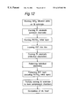
- FIG. 5A is a flowchart for describing the main steps of one example of the methods of producing an ink-jet head of the first embodiment
- FIG. 5B is a flowchart illustrating a different example of the methods.
- FIG. 6 is a front view of the ink-jet head of the first embodiment.
- FIG. 7 is a graph showing a bending amount of the vibration plate relative to an applied voltage in one example of the ink-jet heads of the first embodiment.
- FIG. 8 is a graph showing a bending amount of the vibration plate relative to an applied voltage in another example of the ink-jet heads of the first embodiment.
- FIG. 9 is a sectional view of a piezoelectric vibration section formed on a silicone substrate ( 15 ), illustrating the step of forming the same in process of producing an ink-jet head of the second embodiment of the present invention.
- FIG. 10 is a flowchart for describing the main steps of producing an ink-jet head of the second embodiment.
- FIG. 11 is a partial sectional view of an ink-jet head produced by a method of producing the third embodiment, showing the features of the same.
- FIG. 12 is a flowchart for describing the main steps of the method of producing the ink-jet head of the third embodiment.
- FIG. 13A is a perspective view of an ink-jet head of the fourth embodiment of the present invention.
- FIG. 13B is a sectional view of the ink-jet head taken along line 13 B— 13 B of FIG. 13 A.
- FIG. 14 is a sectional view of the ink-jet head taken along line 14 — 14 of FIG. 13 A.
- FIG. 15 is a partial sectional view of a piezoelectric vibration section of a modification of the fourth embodiment, showing the structure of the same.
- FIG. 16 is a partial sectional view of a preferable bonding structure of the fourth embodiment.
- FIG. 17 is a partial sectional view of another preferable bonding structure of the fourth embodiment.
- FIG. 18 is a partial sectional view of the structure of an ink-jet head of the fifth embodiment according to the present invention.
- FIG. 19 is a perspective view of an ink-jet head of the sixth embodiment according to the present invention.
- An ink-jet head ( 100 ) according to the first embodiment of the present invention comprises a thin piezoelectric film having a large piezoelectric constant, which is formed by what is called a thin-film forming process such as a sputtering process which has hitherto been hardly applied to this field.
- the ink-jet head ( 100 ) of the present invention has features in that it can be made very small in size, having ink outlets which are spaced at narrow intervals to each other, as compared with conventional ink-jet heads.
- FIG. 1A is a perspective view of the ink-jet head ( 100 ) according to the first embodiment of the present invention
- FIG. 1B is a sectional view of the ink-jet head ( 100 ) taken along line 1 B— 1 B.
- the ink-jet head ( 100 ), as shown in FIGS. 1A and 1B, comprises a plurality of outlets ( 2 ); a plurality of compression chambers ( 1 ), each being provided corresponding to each outlet ( 2 ); and a plurality of piezoelectric elements ( 3 ), each being provided for each compression chamber ( 1 ).
- the outlets ( 2 ) are formed at regular intervals in a side plane of the body ( 50 ), and the compression chambers ( 1 ) are formed corresponding to the outlets ( 2 ), respectively, and in parallel with the body ( 50 ).
- Each of the outlets ( 2 ) communicates with each of the compression chamber ( 1 ) through each ink passage ( 2 a ) formed in the body ( 50 ).
- openings ( 51 ) are each formed corresponding to each of the compression chambers ( 1 ) in the top of the body ( 50 ), and also, vibration plates, ( 4 ) are formed on the top of the body ( 50 ) so as to close the openings ( 51 ).
- piezoelectric elements ( 3 ) are each provided on the vibration plate ( 4 ) so as to be positioned on each of the openings ( 51 ), corresponding to each of the compression chambers ( 1 ).
- Each of the piezoelectric elements ( 3 ), as shown in FIG. 2, comprises electrodes ( 6 ) and ( 7 ) each formed from platinum with a thickness of 0.1 ⁇ m; and a piezoelectric film ( 5 ) formed with a thickness of 3 ⁇ m between the electrodes ( 6 ) and ( 7 ), and they are disposed on the vibration plate ( 4 ).
- the vibration plate ( 4 ) is comprised f a SiO 2 layer with a thickness of 2 ⁇ m in the vibrating art.
- a piezoelectric vibration section ( 30 ) is comprised of the piezoelectric element ( 3 ) and the vibration plate ( 4 ).
- PZT perovskite type PZT thin film material which is an oxide of lead, titanium and zirconium
- the abbreviation “PZT” referred to in the description of the specification means a piezoelectric material which contains Pb, Zr and Ti and is represented by the general formula of Pb(Zr x Ti 1-x )O 3 . It is confirmed that, when the composition formula of a PZT thin film is Pb(Zr 0.53 Ti 0.47 )O 3 , the film exhibits maximal piezoelectricity in the form of a sintered body. However, it is difficult to form a thin film of this composition formula directly on the electrode.
- the piezoelectric film ( 5 ) is comprised,of two layers as shown in FIG. 3 .
- a layer of the composition formula of PbTiO 3 , or PLT, i.e. PbTiO 3 and additional lanthanum (La) is formed
- the second layer ( 9 ) a layer of the composition formula of Pb(Zr 0.53 Ti 0.47 )O 3 is formed.
- the piezoelectric film ( 5 ) thus formed is found to be a high quality piezoelectric film having sufficient piezoelectric characteristics.
- the present invention has been achieved based on such a finding that a high-quality piezoelectric film having sufficient piezoelectric characteristics can be provided by forming a first layer of PbTiO 3 containing no Zr or of PLT, i.e. PbTiO 3 to which lanthanum (La) is added, and forming a second layer of Pb(Zr 0.53 Ti 0.47 )O 3 .
- PZT shows excellent piezoelectric characteristics and can have a very high piezoelectric coefficient when the ratio of Zr/Ti is about 50/50.
- the thin film forming process such as the sputtering process, CVD process or the like, and the higher the ratio of Zr to Ti, the more difficult the formation of a sufficient layer.
- an oxide of Zr adsorbs the surface of a substrate in process of forming a thin film and, thereafter, hinders the growth of a film. It is also found that this tendency becomes more significant when a PZT film is allowed to grow on a Pt electrode.
- an excellent PZT film can be formed without deposition of Zr oxide when PZT is allowed to grow by the thin film forming process on a layer of PbTiO 3 or a layer of (Pb, La)TiO 3 (hereinafter referred to as simply “PLT”), that is, a mixture of PbTiO 3 and about 10 mol. % of La which lowers the crystallization temperature.
- PbTiO 3 and PLT have a perovskite structure as well as PZT, and they can be easily formed into films even on Pt electrodes by the thin film forming process. It is necessary for the first layer to have a perovskite structure as an essential requirement.
- the first layer can be formed using an RF sputtering apparatus as well as a PZT layer.
- the first layer ( 8 ) and the second layer ( 9 ) can be formed in sequential steps.
- the piezoelectric film ( 5 ) is comprised of, not such a multi-layer structure but of a first layer having a gradient composition formula in which the composition continuously varies from PbTiO 3 containing no Zn to approximate Pb(Zr 0.5 Ti 0.5 )O 3 .
- first, single crystal of Pt are allowed to orient to form an electrode film with a thickness of 0.1 ⁇ m on an upper face ( 100 ) of a single crystal MgO substrate ( 10 ) of 2 cm square (Step S 1 in FIG. 5 A).
- the Pt electrode film is subjected to patterning into separate and individual electrodes ( 11 ) by dry etching (utilizing actions of Ar ions under vacuum) so as to correspond to the respective compression chambers (Step S 2 in FIG. 5A in connection with FIG. 4 ).
- an initial layer (a first layer) of PbtiO 3 is formed with a thickness of about 0.01 ⁇ m (Step S 3 in FIG. 5 A).
- a PZT thin film is formed with a thickness of about 3 ⁇ m on the initial layer by the sputtering process (Step S 4 in FIG. 5 A).
- the temperature of the substrate is controlled at 500 to 600° C. so as to grow the film in Steps S 3 and S 4 .
- the initial layer of PbTiO 3 is formed before the formation of the PZT thin film, so that there can be formed the single crystal PZT thin film which has the crystals orienting toward the axis c, having little non-uniformity in the composition and having high crystallinity.
- the PZT film shows the highest piezoelectric coefficient in the axial direction c.
- the PZT thin film (including the initial layer) is subjected to patterning by etching using a strong acidic solution, so that the PZT thin film is formed into separate and individual piezoelectric films ( 12 ) which correspond to the respective compression chambers (Step S 5 in FIG. 5A in connection with FIG. 4)
- a common electrode ( 13 ) is formed on the piezoelectric films ( 12 ) (Step S 6 in FIG. 5A in connection with FIG. 4 ).
- the common electrode may be formed as individual electrodes corresponding to the individual piezoelectric films ( 12 ), respectively, as shown in FIG. 4, or it may be formed as a continuous electrode over a plurality of individual piezoelectric films ( 12 ).
- a vibration plate ( 4 ) is formed from SiO 2 with a thickness of 2 ⁇ m on the common electrode ( 13 ) (Step S 7 in FIG. 5 A).
- a resin is packed at both sides of the individual piezoelectric films ( 12 ) to level a surface for forming the vibration plate ( 4 ) before the formation of the vibration plate ( 4 ).
- the vibration plate ( 4 ) is bonded with adhesive to a body which is made of stainless steel and has compression chambers and ink passages previously formed therein.
- the compression chambers and ink passages are formed on the vibration plate (Step S 8 in FIG. 5 A). It is preferable for the adhesive to have a comparatively high hardness so as not to absorb piezoelectrical vibrations.
- the MgO substrate ( 10 ) is removed using an acidic solution (Step S 9 in FIG. 5 A).
- the MgO substrate ( 10 ) can be safely dissolved without any damage on the piezoelectric films by using a phosphoric acid solution as the acidic solution.
- the piezoelectric film and the individual electrodes ( 11 ) are patterned before the formation of the common electrode ( 13 ).
- the present invention is not limited to this method, and the piezoelectric film and the Pt individual electrodes may be subjected to patterning after the formation of the common electrode ( 13 ) and the etching of the MgO substrate ( 10 ) as described in the flowchart in FIG. 5 B.
- a thin piezoelectric film having excellent piezoelectric characteristics can be formed. Further, by applying fine processing techniques for use in production of semiconductors to the resultant thin piezoelectric film, a piezoelectric element which can correspond to a very small compression chamber can be formed, so that an ink-jet head having outlets formed at a high density can be provided.
- the widths of compression chambers are usually set to 100 ⁇ m and those of partition walls between each of the adjacent compression chambers to about 66 ⁇ m.
- the thickness of a PZT thin film is decreased to 5 ⁇ m or less, it becomes possible enough to process the PZT thin film into film strips with a width of 50 ⁇ m or less, so that it makes sure to process the piezoelectric film into shaped films having such a size that can correspond to a compression chamber with a width of 100 ⁇ m.
- FIG. 6 is a front view of a nozzle head having outlets (or nozzles) formed at a density of 200 dpi, provided by the above method.
- the resonance frequency of the compression chamber can be increased, which leads to an advantage that the nozzle head can be driven at a proportionally increased frequency. Further, the drive of the nozzle head at a higher frequency leads to a quicker response to an applied voltage, so that it becomes possible to subtly control the ink-jetting amount. Therefore, the color gradation of a printed image can be improved.
- the resonance frequency is about 1 MHz.
- the ink-jetting performance is generally expressed by a product of bending amount Y and generated pressure P. This value is expressed by the following equation (1), provided that the thickness of a piezoelectric film is t, the piezoelectric constant is d 31 , and the voltage is V. Accordingly, this provides an advantage that the use of a thin film makes it possible to decrease the voltage applied.
- a PZT thin film in which the ratio of Zr/Ti is 50/50 is subjected to patterning so as to obtain samples each having a width of 10 ⁇ m and a length of 1 mm which correspond to each of the compression chambers ( 1 ).
- a relationship between an applied voltage and a maximal bending amount of a vibration plate ( 4 ) was measured.
- FIG. 7 shows the results. It is known from the graph shown in FIG. 7 that the application of an increased voltage bends the vibration plate and that the vibration plate is displaced by about 2 ⁇ m relative to the application of 30 V. Thus, it is confirmed that an ink-jet head having high ink-jetting performance can be provided by utilizing the above excellent piezoelectric characteristics.
- the ink-jet head of the first embodiment is formed by processing the thin piezoelectric film ( 5 ) which has excellent piezoelectric characteristics and which is composed of the perovskite type first layer containing no Zr and the second layer formed from PZT containing Zr. By doing so, finely processed piezoelectric films ( 5 ) having excellent piezoelectric characteristics can be formed. Therefore, there can be provided an ink-jet head which is made very small in size and has ink outlets formed therein at a high density, as compared with the conventional ink-jet heads.
- the first layer (the initial layer) of the piezoelectric film As for the first layer (the initial layer) of the piezoelectric film, the first layer ( 8 ) is provided to form the second layer ( 9 ) having high crystallinity as mentioned above, and it is to be noted that the second layer ( 9 ) is dominantly responsible for the function exhibiting piezoelectricity. Therefore, the thinner the first layer ( 8 ), the better, to an extent that the first layer ( 8 ) can have a function serving to form an excellent second layer and that the piezoelectric characteristics of the piezoelectric film ( 5 ) as a whole do not decrease. We have confirmed that the first layer ( 8 ) can sufficiently exhibit its function even if it is 5 nm or less in thickness when a sputtering apparatus which is excellent in film thickness controllability is used.
- the thickness of the first layer is controlled within a range of 50 to 100 nm in consideration of uniform coating of the Pt electrode and control of the production steps. Within this range, a substantial degradation in the piezoelectric characteristics of the piezoelectric film ( 5 ) as a whole can be prevented, and the first layer can sufficiently contribute to formation of a high quality second layer, and also, additional burdens for controlling the steps of forming the piezoelectric film ( 5 ) can be decreased.
- the first layer ( 8 ) as a PbTiO 3 layer with a thickness of 0.1 ⁇ m and the second layer ( 9 ) as a PZT layer with a thickness of 2.9 ⁇ m having a composition formula of Pb(Zr 0.53 Ti 0.47 )O 3 , there can be provided an ink-jet head capable of exhibiting a sufficient ink-jetting ability even at a low voltage.
- the thickness of the second layer ( 9 ) composed of PZT is not particularly limited. However, it is preferable that the thickness of the second layer ( 9 ) is controlled to 10 ⁇ m or less, because, when the second layer is formed by the thin film forming process, it takes long time in forming the film if the thickness of the second layer becomes large. In the meantime, after formed, the piezoelectric film ( 5 ) is subjected to patterning so as to have a given shape and size corresponding to each of the compression chambers.
- the thickness of the piezoelectric film ( 5 ) is controlled to 5 ⁇ m or less so as to achieve accurate patterning which can correspond to the intervals between each of the ink outlets ( 2 ) which are considered to be more necessary to be still narrower in future.
- the thickness of the piezoelectric film ( 5 ) is controlled to 0.5 ⁇ m or more in consideration of the strength of the film and a stress which would occur. According to our examination, it is the most preferable that the thickness of the piezoelectric film ( 5 ) is controlled within a range of 1 to 3 ⁇ m. It is confirmed within this range that ink droplets can stably jet and that the reliability of the film can be maintained constant or higher.
- the body ( 50 ) is formed from stainless steel (SUS), but it may be formed from a photosensitive organic polymeric material, photosensitive glass, silicone or the like other than stainless steel.
- SUS stainless steel
- the vibration plate ( 4 ) is formed from silicon dioxide (SiO 2 ), but it may be formed from a metal such as nickel, chrome, aluminum or the like other than silicon oxide.
- the vibration plate can be easily formed from any of these metals by the sputtering process, vacuum deposition process, or metallizing plating process, having vibration characteristics as excellent as those of the SiO 2 vibration plate.
- a vibration plate ( 4 ) formed from alumina can exhibit a similar effect to that of the SiO 2 vibration plate, and it also can be easily formed by the sputtering process.
- a polyimide resin can be used to form a vibration plate ( 4 ), and the vibration plate ( 4 ) can be easily formed from a polyimide resin by the spin-coating process, and its fine processing is also easy.
- polyimide resins are found to be suitable materials for vibration plates of ink-jet recorders.
- vibration plates ( 4 ) formed from the above-listed materials shows no degradation such as cracks which occur during the vibrating operation, and they can sufficiently vibrate to jet ink droplets. Further, vibration plates ( 4 ) formed from oxides of the above-listed metals can exhibit the same vibration characteristics as those of the vibration plate formed from the above metals. Further, the use of a vibration plate ( 4 ) formed from photosensitive polyimide is effective to facilitate the formation of piezoelectric elements.
- the vibration plate ( 4 ) which faces the compression chamber ( 1 ) a SiO 2 layer having a thickness of 2 ⁇ m is used; as the second layer ( 9 ) of the piezoelectric film ( 5 ), a PZT thin film of the composition formula of Pb(Zr 0.5 Ti 0.5 )O 3 , having a thickness of 3 ⁇ m is used; and as the electrodes ( 6 ) and ( 7 ), platinum layers having a thickness of 0.1 ⁇ m are used. Under the above conditions, the vibration plate ( 4 ) can be caused to sufficiently generate flexural vibration even by application of 50 V or less.
- the thickness of the vibration plate ( 4 ) is not limited to 2 ⁇ m as specified above, and the thickness of the vibration plate ( 4 ) should be selected appropriately, taking into account the piezoelectric characteristics and thickness of the piezoelectric film ( 5 ), the inherent vibration characteristics of materials forming the vibration plate ( 4 ) and the like.
- the piezoelectric films ( 5 , 12 ) composed of lead-based dielectric layers having perovskite structures can be provided having good crystallinity.
- the piezoelectric films ( 5 , 12 ) which have a little variation in the characteristics can be formed on an electrode formed from any of the above-listed materials, so that variation in ink-jetting ability between each of the elements can be decreased.
- PZT for use as a piezoelectric material for the second layer which constitutes the piezoelectric films ( 5 , 12 ), is formed into a PZT layer in which the ratio of Zr/Ti is from 30/70 to 70/30 to impart the PZT layer excellent piezoelectric characteristics.
- other than PZT for example, piezoelectric materials which contain other elements than Pb, Ti and Zr, and have the composition formula of Pb 0.99 Nb 0.02 [(Zr 0.6 Sn 0.4 ) 1-y Ti y ] 0.98 O 3 (0.060 ⁇ y ⁇ 0.065) may be used as piezoelectric materials for the second layer.
- the graph in FIG. 8 shows a relationship between a voltage applied and the maximal displacement of the vibration plate ( 4 ) in this case.
- a voltage of 15 V When a voltage of 15 V is applied, a phase change from the antiferroelectrics to ferroelectrics occurs, so that discontinuous displacement characteristics are shown.
- the vibration plate ( 4 ) shows displacement of about 0.8 ⁇ m.
- a piezoelectric element which has a stable ink-jetting ability in spite of being a polycrystalline thin film when the antiferroelectric thin film of the composition formula of Pb 0.99 Nb 0.02 [(Zr 0.6 Sn 0.4 ) 1-y Ti y ] 0.98 O 3 (0.060 ⁇ y ⁇ 0.065) is used.
- the piezoelectric films there is given such one that comprises the first layer ( 8 ) composed of a layer of PbTiO 3 containing no Zr, or of a layer of PLT which contains PbTiO 3 and additional lanthenum (La), and the second layer ( 9 ) composed of a layer of Pb(Zr 0.53 Ti 0.47 )O 3 .
- the present invention is not limited to this piezoelectric film.
- a second layer having good crystallinity and a comparatively large piezoelectric constant can be formed when a PZT layer of the composition formula of Pb(Zr x Ti 1-x )O 3 (x ⁇ 0.3) or the PZT layer further containing La is used as the piezoelectric material for the first layer (the initial layer) which constitutes the piezoelectric films ( 5 , 12 ), and a PZT layer of the composition formula of Pb(Zr x Ti 1-x )O 3 (0.7 ⁇ 0.3) is used as the second layer.
- a PZT layer of the composition formula of Pb(Zr x Ti 1-x )O 3 (X ⁇ 0.2) or the PZT layer further containing La is used as the first layer.
- FIGS. 9 and 10 illustrate the method of producing an ink-jet head according to the second embodiment of the present invention.
- the production method for the second embodiment is almost the same as that for the first embodiment except that a silicone (Si) substrate is used instead of the-MgO substrate used in the first embodiment.
- a Pt layer for forming individual electrodes ( 11 ) is formed on a silicone substrate ( 15 ), and a piezoelectric film ( 12 ) composed of lead-based dielectric layer is formed as a piezoelectric material on the individual electrodes ( 11 ) by the sputtering process.
- the piezoelectric film ( 12 ) composed of the lead-based dielectric layer is provided by forming a first layer from a lead-based dielectric material containing no Zr, and then, forming a second layer from PZT containing Zr as in the first embodiment.
- the piezoelectric film ( 12 ) thus formed is of polycrystalline
- the second layer which has very excellent piezoelectric characteristics can be formed because the first layer is formed from the lead-based dielectric material containing no Zr, and then, the second layer is formed from PZT containing Zr.
- the piezoelectric film ( 12 ) can have excellent piezoelectricity by forming a PZT-based polycrystalline layer with a thickness of 3 ⁇ m.
- a piezoelectric thin film having high crystallinity can be formed by the spin-coating process using MOCVD or a sol-gel solution instead of the above-mentioned sputtering process.
- a Pt layer for a common electrode ( 13 ) is formed on the piezoelectric film ( 12 ).
- a sol-gel solution containing no Zr is applied to form-the first layer, and then, a sol-gel solution containing Zr is applied to the first layer so as to form the second layer with a given thickness, and the layers are baked to form a piezoelectric film ( 12 ).
- the piezoelectric film ( 12 ) which is a polycrystalline layer can be formed as well as that formed by the sputtering process.
- a vibration plate ( 4 ) is formed from a material of SiO 2 on the common electrode ( 13 ) by the sputtering process.
- a body having compression chambers ( 1 ) formed therein from a photosensitive resin is assembled on the vibration plate ( 4 ), and finally, the silicone substrate ( 15 ) is removed by etching using a hydrofluoric acid solution or a potassium hydroxide solution.
- the compression chambers ( 1 ) divided in the body so as to correspond to the outlets, respectively, are formed from a photosensitive glass or a photosensitive resin.
- the individual electrodes ( 11 ) are formed by patterning before the formation of the piezoelectric film ( 12 ), but the individual electrodes ( 11 ) may be formed by patterning after the etching of the silicone substrate ( 15 ). Also, the piezoelectric film ( 12 ) is subjected to patterning before the formation of the common electrode ( 13 ) in the flowchart of FIG. 10, but the piezoelectric film ( 12 ) may be patterned so as to be divided into shaped pieces which correspond to the divided compression chambers ( 1 ) after the etching of the silicone substrate ( 15 ).
- the production method described in the present embodiment it becomes possible to use a silicone substrate ( 15 ) which is a more available single crystal substrate capable of having a larger area at a lower cost than the MgO substrate ( 10 ). Therefore, it becomes possible to form a plurality of piezoelectric elements for jetting ink droplets at once and further to form thin film materials having excellent piezoelectric characteristics. Further, the fine processing techniques which have been established in the filed of silicones can be applied to the piezoelectric elements, and this facilitates multi-element formation which would be achieved by very high accurate fine processing.
- the ink-jet head produced by the above method can have the same structure as shown in FIG. 6, having nozzles at a density of 200 dpi. Furthermore, it is possible to produce an ink-jet head having nozzles at a higher density.
- a glass substrate may be used, and it is possible to produce an ink-jet head which has a similar multi-element formation structure by using a glass substrate.
- the glass substrate is removed by etching using a hydrofluoric acid solution.
- an ink-jet head having the same multi-element formation structure as that shown in FIG. 6 can be provided.
- a piezoelectric film ( 12 ) having a perovskite structure and a high crystallinity can be formed by using a ruthenium oxide for the above individual electrodes ( 11 ) other than platinum.
- the piezoelectric film therefore, can have excellent characteristics, so that an ink-jet head having a little variation in the ink-jetting ability between each of the elements can be provided in spite of having the multi-element formation structure.
- a PZT layer having a ratio of Zr/Ti within a range of 30/70 to 70/30 shows further excellent piezoelectric characteristics, thus providing an ink-jet head having a high ink-jetting ability.
- the materials for the vibration plate ( 4 ) besides silicon dioxide (SiO 2 ), metals such as nickel and aluminium can be easily formed into films by the sputtering process, vacuum deposition process or metallizing plating process, and the resultant films can show excellent vibration characteristics as well as the SiO 2 vibration plate. Furthermore, a vibration plate formed from an oxide such as alumina or the like can provide the same effect as that obtained by the SiO 2 vibration plate, and the oxide such as alumina or the like can be easily formed into a film by the sputtering process. Otherwise, high molecular organic substances such as polyimide resins can be easily formed into films by the spin coating process, and the processing thereof is also easy. Thus, high molecular organic substances such as polyimide resins are found to be suitable materials for the vibration plates of ink-jet heads.
- a vibration plate ( 4 ) is formed from silicon dioxide (SiO 2 ) with a thickness of 2 ⁇ m on a silicone substrate ( 15 ) by the sputtering process, or by thermally oxidizing the silicone substrate. Then, a Pt layer for a common electrode ( 13 ) is further formed on the vibration plate ( 4 ). Then, a piezoelectric film ( 12 ) formed from a lead-based dielectric material is formed on the common electrode ( 13 ) by the rf sputtering process.
- the piezoelectric film ( 12 ) is formed by forming a first layer from a lead-based dielectric material containing no Zr and forming a second layer from PZT containing Zr.
- the piezoelectric film ( 12 ) thus formed is of polycrystalline, but can comprise the second layer having very excellent piezoelectric characteristics, because the second layer composed of the PZT layer containing Zr is formed after the formation of the first layer composed of the lead-based dielectric material containing no Zr.
- the piezoelectric film ( 12 ) can obtain excellent piezoelectric characteristics by forming a PZT type polycrystalline layer with a thickness of 3 ⁇ m.
- a piezoelectric thin film having a high crystallinity can be formed also by the spin-coating process using MOCVD or a sol-gel solution.
- a Pt layer for individual electrodes ( 11 ) is formed on the piezoelectric film ( 12 ).
- the individual electrodes ( 11 ) are formed by subjecting the Pt layer to fine processing through ion etching so as to be formed into divided shaped pieces which correspond to the respective compression chambers ( 1 ).
- the vibration plate ( 4 ) is formed from an insulating substance, the individual electrodes ( 11 ) may be formed on the vibration plate ( 4 ), and the common electrode ( 13 ) may be formed on the piezoelectric film ( 12 ).
- the silicone substrate ( 15 ) is partially removed by etching using a hydrofluoric acid solution or a potassium hydroxide solution, and the remaining parts of the silicone substrate ( 15 ) are used as the structural parts of the compression chambers ( 1 ).
- the piezoelectric film ( 12 ) is subjected to patterning so as to be divided into shaped pieces which correspond to the respective compression chambers ( 1 ) before the formation of the common electrode ( 13 ).
- the compression chambers ( 1 ) are formed by using parts of the substrate for forming the piezoelectric element, so that the production step can be simplified. Furthermore, it becomes possible to provide finely formed elements by applying the fine processing techniques for silicones.
- the ink-jet head produced by the above method can have the same structure as that shown in FIG. 6, having nozzles at a density of 200 dpi or more.
- a more inexpensive glass substrate can be used other than the silicone substrate ( 15 ), and also, by using the glass substrate, an ink-jet head having the same multi-element formation structure as that shown in FIG. 6 can be provided.
- a piezoelectric film ( 12 ) having a perovskite structure with a high crystallinity can be formed.
- the piezoelectric film can have excellent properties, so that there can be provided an ink-jet head having a little variation in ink-jetting ability between each of the piezoelectric elements in spite of having the multi-element formation structure.
- the piezoelectric film ( 12 ) to be used as a piezoelectric material is a PZT layer having a Zr/Ti ratio within the range of 30/70 to 70/30, the piezoelectric material can have further excellent piezoelectric characteristics, and the resultant ink-jet head can have high ink-jetting ability.
- an antiferroelectric thin film of the composition formula of Pb 0.99 Nb 0.02 [(Zr 0.6 Sn 0.4 ) 1-y Ti y ] 0.98 O 3 (0.060 ⁇ y ⁇ 0.65) is used as the piezoelectric film ( 12 )
- a piezoelectric element formed of the above film can stably respond to a voltage applied, and is decreased in variation in ink-jetting amount.
- an antiferroelectric thin film of the composition formula of Pb 0.99 Nb 0.02 [(Zr 0.6 Sn 0.4 ) 1-y Ti y ] 0.98 O 3 (0.060 ⁇ y ⁇ 0.065) is used as the piezoelectric film
- a piezoelectric element which has a stable ink-jetting ability even when formed of a polycrystalline thin film.
- the vibration plate ( 4 ) can be easily formed from a metal such as nickel and aluminium other than silicon dioxide SiO 2 by the sputtering process, vacuum deposition process or metallizing plating process, and the resultant vibration plate ( 4 ) can have excellent vibration characteristics as well as the SiO 2 vibration plate.
- alumina can be used to form a vibration plate, and the alumina vibration plate can be easily formed by the sputtering process, and provide the same effect as the SiO 2 vibration plate.
- the vibration plate can be easily formed from a polyimide resin by the spin-coating process, and the processing of the polyimide resin vibration plate is also easy.
- polyimide resins are found to be suitable materials for ink-jet heads.
- FIG. 13A is a perspective view of an ink-jet head ( 200 ) according to the fourth embodiment of the present invention
- FIG. 13B is a sectional view of the same taken along line 13 B- 13 B of FIG. 13A
- FIG. 14 is a sectional view of the same taken along line 14 — 14 of FIG. 13 A.
- the ink-jet head ( 200 ) comprises a body ( 250 ) having a plurality of outlets ( 202 ) and a plurality of compression chambers ( 201 ) formed corresponding to the plurality of outlets ( 202 ), respectively; a vibration plate ( 204 ) provided on top of the body ( 250 ); and a piezoelectric element ( 203 ) provided on the vibration plate ( 204 ).
- the outlets ( 202 ) are formed at predetermined intervals in the lower plane of the body ( 250 ), and the compression chambers ( 201 ) are formed in parallel with the body ( 250 ) and corresponding to the outlets ( 202 ), respectively.
- Each of the outlets ( 202 ) communicates with each of the compression chambers ( 201 ) through an ink passage ( 202 a ) formed in the body ( 250 ).
- the body ( 250 ) is formed from a highly rigid material such as a resin, glass, stainless steel, ceramics, silicone or the like.
- the piezoelectric element ( 203 ) comprises, as shown in FIG. 14, a common electrode ( 208 ) formed on the vibration plate ( 204 ); piezoelectric films ( 205 ) formed on the common electrode ( 208 ) at predetermined intervals corresponding to the compression chambers ( 201 ), respectively; and individual electrodes ( 209 ) provided on the piezoelectric films ( 205 ), respectively, and further, a filler of a polyimide resin is packed in the spaces between each of the piezoelectric films ( 5 ) adjacent to each other.
- the piezoelectric film ( 205 ) is formed having a first layer ( 8 ) composed of a layer of PbTiO 3 containing no Zr, or PLT containing PbTiO 3 and lanthanum, and a second layer ( 9 ) composed of a layer of the composition formula of Pb(Zr 0.53 Ti 0.47 )O 3 with a thickness of about 3 ⁇ m, as in the first embodiment.
- the piezoelectric film ( 205 ) having excellent piezoelectric characteristics is formed as well as that of the first embodiment.
- the vibration plate ( 204 ) is comprised of an alumina layer which is formed with a thickness of 2 ⁇ m by the sputtering process, and both the common electrode ( 208 ) and the individual electrodes ( 209 ) are comprised of Pt layers with a thickness of 0.1 ⁇ m, respectively.
- the materials for the vibration plate ( 204 ) Ni, Cr, Ti, Al and Zr can be used other than alumina, and any of the materials can provide a vibration plate which is excellent in adhesion to the piezoelectric film ( 205 ) and the electrode material and in vibration characteristics.
- oxides of Ni, Cr, Ti, Al and Zr, silicon oxide, and resins can be used as the materials for the vibration plate ( 204 ).
- the thickness of the vibration plate ( 204 ) is equal to or smaller than that of the piezoelectric film ( 205 ) so as to obtain excellent ink-jetting ability.
- the piezoelectric film ( 205 ) is formed with a narrower width than that of the compression chamber to which the piezoelectric film ( 205 ) correspond.
- the present invention is not limited to the above piezoelectric film ( 205 ).
- a single undivided and continuous piezoelectric film may be used instead of the divided piezoelectric films, and the individual electrodes ( 209 ) may be formed so as to correspond to the compression chambers ( 201 ), respectively.
- ink droplets are jetted by vibrating only parts of the piezoelectric layer that correspond to some of the compression chambers.
- the material for the filler ( 210 ) to be packed between each of the piezoelectric films ( 205 ) adjacent to each other is not limited to the polyimide resin as mentioned above, and any material that has a comparatively low rigidity can be used.
- the use of a comparatively low rigid material as the filler makes it possible to vibrate the piezoelectric film ( 205 ) without preventing lateral expansion or contraction of the piezoelectric film ( 205 ). Therefore, the vibration characteristics do not degrade.
- each of the compression chambers ( 201 ) is formed with a width of 70 ⁇ m and the piezoelectric film ( 205 ) with a width slightly narrower than that of the compression chamber ( 201 ), the vibration amplitude can be changed by maximum 50 nm when a voltage of 10 V is applied.
- the piezoelectric film ( 205 ) is formed having the first layer and the second layer as a two-layer structure by the thin film forming process such as the sputtering process as in the first embodiment. Therefore, the piezoelectric film ( 205 ) can have a very high density, high crystallinity, and excellent vibration characteristics despite of the comparatively simple structure. This is because the formation of the piezoelectric film ( 205 ) having a high crystallinity makes it possible for the piezoelectric element to be driven by application of such a high voltage that would cause a conventional sintered body to be dielectrically broken down.
- the piezoelectric film ( 205 ) can be formed with a very small thickness as in the first embodiment, fine processing can be easily conducted on such a film, so that an ink-jet head having nozzles at a density of 200 dpi can be easily produced.
- the piezoelectric film ( 205 ) may be formed by the thin film forming process such as CVD process other than the spin coating process as mentioned above.
- the thickness of the piezoelectric film ( 205 ) is preferably 10 ⁇ m or less because, when it is 10 ⁇ m or more, fine processing is hardly done on it.
- the piezoelectric film ( 205 ) is formed by using an MgO substrate or a Si substrate as in the first or second embodiment.
- a single crystal MgO substrate which is cleavaged to have a plane ( 100 ) as the surface is used, and an initial layer containing no Zr is formed on the plane ( 100 ) of the MgO substrate. Then, a piezoelectric film of the general formula of (Pb 1-x La x ) (Zr 1-y Ti y )O 3 is formed on the initial layer so as to form a piezoelectric film in which the crystals orient in a direction of the axis c.
- the addition of La to the piezoelectric film represented by the general formula of Pb(Zr 1-y Ti y )O 3 decreases the crystallization temperature, so that the piezoelectricity of the piezoelectric thin film can be improved.
- the single crystal piezoelectric film of the formula of (Pb 1-x La x ) (Zr 1-y Ti y )O 3 thus formed can have a piezoelectric constant 1.5 times as large as that of a polycrystalline film of the same composition.
- the piezoelectric film ( 205 ) by using the sputtering process or the CVD process, a single crystal film having high crystallinity can be formed at a high deposition rate of 1 ⁇ m or more per hour. Furthermore, by using platinum or ruthenium oxide as the material for the electrode, the piezoelectric film can grow while maintaining good interface properties. When platinum or ruthenium oxide is used for the electrode, it becomes possible to use, other than magnesium oxide (MgO), silicone, glass, or stainless steel material which has a high rigidity and can be finely processed with ease, as the material for the substrate. As a result, the production cost for ink-jet heads can be reduced.
- MgO magnesium oxide
- silicone silicone
- glass glass
- stainless steel material which has a high rigidity and can be finely processed with ease
- the piezoelectric film ( 205 ) having high crystallinity can be formed because deposition of an impurity layer of Zr on the electrode can be prevented by particularly adjusting the value of y to 0.7 or more (by decreasing the amount of Zr) in the composition formula of a part of the piezoelectric film in contact with the electrode.
- the piezoelectric film ( 205 ) having a large piezoelectric constant can be formed with high crystallinity.
- the ink-jet head of the present invention comprises a thin piezoelectric film and a vibration plate as mentioned above, it is necessary to take care in bonding the body having the compression chambers formed therein to the vibration plate. That is, when the partition walls of the body are bonded to the vibration plate with adhesive, a large stress is applied to the thin piezoelectric film ( 205 ) because of the expansion or contraction of the adhesive in process of the curing thereof, so that the film cracks or peels. Even though the film could not be so damaged as to crack or peel, stable vibration would be hindered.
- the partition walls ( 207 ) of the body are bonded to the vibration plate ( 204 ) through a resin layer ( 212 ) which has a thickness of 2 ⁇ m or so and a low rigidity as shown in FIG. 16 .
- the resin layer ( 212 ) is formed from, for example, polyimide by the spin coating process or the like.
- number 213 which appears in FIG. 16 refers to the adhesive.
- the polyimide resin layer ( 212 ) As described above, by providing the polyimide resin layer ( 212 ), a stress due to expansion or contraction of the adhesive ( 213 ) can be prevented from applying to the piezoelectric film ( 205 ), so that the piezoelectric film can be stably vibrated, and simultaneously damage of the piezoelectric film can be prevented. Further, by providing the polyimide resin layer, an ink can be avoided from directly contacting the vibration plate, so that the life of the vibration plate can last longer. In this regard, it is preferable that the thickness of the resin layer ( 212 ) is 3 ⁇ m less. When it is 3 ⁇ m or more, the resin layer absorbs the vibrations of the vibration plate, so that the ink-jetting performance significantly degrades.
- an alumina layer ( 214 ) with a thickness of 7 ⁇ m is seen to be formed on parts of the piezoelectric vibration section ( 230 ) (comprising the piezoelectric element and the vibration plate) to which the partition walls are bonded.
- the alumina layer ( 214 ) is formed as follows: an alumina layer is formed with a thickness of 7 ⁇ m on the piezoelectric vibration section ( 230 ) and, then, the alumina layer is subjected to wet etching using an acidic solution so that the parts of the alumina layer which correspond to the partition walls can be left to remain.
- the partition walls ( 207 ) to the piezoelectric vibration section ( 230 ) through the alumina layer ( 214 )
- only parts of the piezoelectric vibration section ( 230 ) which correspond to the compression chambers ( 201 ) can be vibrated, so that the variation in the ink-jetting amount or the like can be decreased.
- a layer which is formed from ceramics composed of various metal oxides, a highly rigid resin such as an epoxy resin, Cr or the like may be used instead of the alumina layer ( 214 ). That is, any material that shows good adhesion to the piezoelectric vibration section ( 230 ) and permits fine processing can be used.
- the piezoelectric film ( 205 ) is composed of one layer, but the piezoelectric film of the present invention is not limited to the above one-layer structure, and it may have two layers, i.e. the piezoelectric films 205 a and 205 b . as shown in FIG. 15 .
- the individual electrode ( 209 ) is formed as separate electrodes ( 209 a ) and ( 209 b ), wherein the electrode ( 209 a ) is formed on the piezoelectric film ( 205 a ) and the electrode ( 209 b ) is formed on the underside of the piezoelectric film ( 205 b ), and an intermediate electrode ( 211 ) as a common grounding electrode is formed between the piezoelectric films ( 205 a ) and ( 205 b ).
- the piezoelectric vibration section can show displacement two times larger than that shown by a piezoelectric vibration section comprising one piezoelectric film.
- each of the piezoelectric films ( 205 a ) and ( 205 b ) comprises an initial layer (a first layer) and a second layer.
- the piezoelectric vibration section generate flexural vibration by using the piezoelectric films ( 205 a ) and ( 205 b ), so that theoretically, it becomes unnecessary to provide the vibration plate ( 204 ) which is caused to vibrate in cooperation with the piezoelectric film.
- the piezoelectric vibration section can be provided by forming two piezoelectric films ( 205 a ) and ( 205 b ) without the need to provide a vibration plate.
- FIG. 18 is a partial sectional view of an ink-jet head according to the fifth embodiment of the present invention, illustrating the structure of the ink-jet head.
- the ink-jet head according to the fifth embodiment is produced by the following steps.
- a Pt layer for a common electrode ( 208 ) is formed on a single crystal silicone substrate, and piezoelectric films ( 205 ) with a thickness of 3 ⁇ m and individual electrodes ( 209 ) each corresponding to each of compression chambers, are formed on the common electrode ( 208 ) in the same manner as in the first embodiment. Then, alumina layer with a thickness of 2 ⁇ m as vibration plates ( 204 a ) are formed on the individual electrodes ( 209 ). A filler polyimide resin ( 210 ) is packed in the space between each of the piezoelectric films ( 205 ) adjacent to each other.
- the silicone substrate is polished to a thickness of about 0.1 mm, and the polished silicone substrate is subjected to etching using an alkaline solution such as an aqueous KOH solution, so that parts of the silicone substrate (silicone bases ( 15 )) which correspond to the partition walls for separating the compression chambers, respectively, are left to remain.
- the partition walls of a body, which has the compression chambers formed therein from a stainless steel, resin or glass, are faced to the silicone bases ( 15 ) and bonded thereto.
- the ink-jet head according to the fifth embodiment shown in FIG. 18 is completed.
- the width of the compression chamber ( 201 ) is 70 ⁇ m.
- the silicone substrate is finely processed, and parts of the silicone substrate are used to form the compression chambers, and the adhesion parts of the body are kept distant from the piezoelectric films. Therefore, degradation of the vibration characteristics due to the affection of the adhesion parts can be substantially eliminated. As a result, in the ink-jet head of the fifth embodiment, the variation in the ink-jetting performance can be significantly decreased.
- quartz glass may be used for the substrate instead of silicone.
- the use of quartz glass for the substrate makes it possible to finely process the substrate through etching using hydrofluoric acid, so that the ink-jet head can be produced at a still lower cost.
- a piezoelectric film ( 205 ) of the composition formula of Pb(Zr 0.53 Ti 0.47 )O 3 in which the crystals orient in the direction of axis c, can be formed through the initial layer on the Pt electrodes as described in the first embodiment.
- the resultant piezoelectric film can have a piezoelectric constant about 1.5 times larger than that of a piezoelectric film comprised of a polycrystalline thin film of the same composition formula.
- the substrate is similarly polished or etched to a thickness of about 0.1 mm, and then processed as shown in FIG. 18, and the processed portions are bonded to the partition walls of the body.
- FIG. 19 is a perspective view of an ink-jet head according to the sixth embodiment of the present invention.
- the ink-jet head of the sixth embodiment comprises a body ( 350 ) composed of lamination of four stainless steel plates ( 351 , 352 , 353 and 354 ), and a piezoelectric vibration section (comprised of a piezoelectric element ( 303 ) and a vibration plate ( 304 )) so provided as to close compression chambers ( 301 ) which are formed in the body ( 350 ).
- ink outlets ( 302 ) are formed along the width direction in parallel with each other in the underside of the stainless plate ( 354 ).
- the ink chambers ( 301 ) which are divided by the partition walls (not shown) are provided corresponding to the ink outlets ( 302 ), respectively.
- the piezoelectric element ( 303 ) comprises a common electrode (not shown), a piezoelectric film ( 305 ) and individual electrodes ( 309 ). Each of the individual electrodes ( 309 ) is formed directly on each of the compression chambers ( 301 ), and thus, individual piezoelectric elements which correspond to the compression chambers ( 301 ), respectively, are provided.
- the piezoelectric film ( 305 ) is formed in the same manner as in the first to fifth embodiments.
- the body ( 350 ) is composed of the stainless steel plates ( 351 ) to ( 354 ), but the present invention is not limited to this structure, and the body ( 350 ) may be composed of lamination of glass plates. Further, the body having the structure shown in FIG. 19 may be as be formed using resin plates.
- the present invention it becomes possible to form piezoelectric films having smaller thickness and larger piezoelectric constants in comparison with the prior art, by using the thin film forming process such as the sputtering process and CVD process, so that it makes possible to finely process the piezoelectric films. Therefore, miniaturized ink heads for in-jet recorders which have ink outlets formed at higher densities and can respond at higher speeds can be provided. By using the miniaturized ink-jet heads having outlets formed at high densities therein, it becomes possible to provide ink-jet recorders which permit high-speed printing with high resolution.
Landscapes
- Engineering & Computer Science (AREA)
- Manufacturing & Machinery (AREA)
- Particle Formation And Scattering Control In Inkjet Printers (AREA)
Abstract
Description
Claims (20)
Applications Claiming Priority (3)
| Application Number | Priority Date | Filing Date | Title |
|---|---|---|---|
| JP9-095491 | 1997-04-14 | ||
| JP09549197A JP3666177B2 (en) | 1997-04-14 | 1997-04-14 | Inkjet recording device |
| PCT/JP1998/001691 WO1998046429A1 (en) | 1997-04-14 | 1998-04-14 | Ink-jet head |
Publications (1)
| Publication Number | Publication Date |
|---|---|
| US6347862B1 true US6347862B1 (en) | 2002-02-19 |
Family
ID=14139077
Family Applications (1)
| Application Number | Title | Priority Date | Filing Date |
|---|---|---|---|
| US09/202,419 Expired - Lifetime US6347862B1 (en) | 1997-04-14 | 1998-04-14 | Ink-jet head |
Country Status (6)
| Country | Link |
|---|---|
| US (1) | US6347862B1 (en) |
| EP (1) | EP0930165B1 (en) |
| JP (1) | JP3666177B2 (en) |
| KR (1) | KR100309405B1 (en) |
| DE (1) | DE69818793T2 (en) |
| WO (1) | WO1998046429A1 (en) |
Cited By (52)
| Publication number | Priority date | Publication date | Assignee | Title |
|---|---|---|---|---|
| US20020066524A1 (en) * | 2000-10-19 | 2002-06-06 | Yutaka Kagawa | Piezoelectric film type actuator, liquid discharge head, and method of manufacturing the same |
| US20020140320A1 (en) * | 2001-02-09 | 2002-10-03 | Akira Unno | Piezoelectric structure, liquid ejecting head and manufacturing method therefor |
| US20020158947A1 (en) * | 2001-04-27 | 2002-10-31 | Isaku Kanno | Piezoelectric element, method for manufacturing piezoelectric element, and ink jet head and ink jet recording apparatus having piezoelectric element |
| US6547376B1 (en) * | 1999-04-21 | 2003-04-15 | Matsushita Electric Industrial Co., Ltd. | Ink jet head and method for the manufacture thereof |
| US20030173871A1 (en) * | 2000-07-24 | 2003-09-18 | Isaku Kanno | Thin-film piezoelectric element |
| US6623110B2 (en) * | 1998-10-20 | 2003-09-23 | Fujitsu, Limited | Ink jet recording head and production methods therefor and printer apparatus therewith |
| US20040021745A1 (en) * | 2002-07-18 | 2004-02-05 | Canon Kabushiki Kaisha | Manufacturing method fo liquid jet head |
| US20040025343A1 (en) * | 1999-12-10 | 2004-02-12 | Fujitsu Limited | Ink jet head, method of manufacturing ink jet head, and printer |
| US20050127780A1 (en) * | 2003-12-10 | 2005-06-16 | Canon Kabushiki Kaisha | Dielectric thin film element, piezoelectric actuator and liquid discharge head, and method for manufacturing the same |
| US20050185026A1 (en) * | 2004-01-26 | 2005-08-25 | Motohisa Noguchi | Piezoelectric element, piezoelectric actuator, ink jet recording head, ink jet printer, surface acoustic wave element, frequency filter, oscillator, electronic circuit, thin film piezoelectric resonator, and electronic apparatus |
| US20050195228A1 (en) * | 2004-03-03 | 2005-09-08 | Fuji Photo Film Co., Ltd. | Liquid discharge head and manufacturing method thereof |
| US20050258719A1 (en) * | 2004-05-19 | 2005-11-24 | Brother Kogyo Kabushiki Kaisha | Piezoelectric actuator, ink-jet head provided with the same, ink-jet printer, and method for manufacturing piezoelectric actuator |
| US20060012644A1 (en) * | 2004-07-13 | 2006-01-19 | Brother Kogyo Kabushiki Kaisha | Ink jet head, piezo-electric actuator, and method of manufacturing them |
| US20060012646A1 (en) * | 2004-07-13 | 2006-01-19 | Brother Kogyo Kabushiki Kaisha | Piezoelectric actuator, ink jet head, and method of manufacturing them |
| US20060044359A1 (en) * | 2004-08-31 | 2006-03-02 | Brother Kogyo Kabushiki Kaisha | Piezoelectric actuator having piezoelectric layer and vibration plate with groove, liquid transporting apparatus, and method of manufacturing liquid transporting apparatus |
| US20060049723A1 (en) * | 2004-09-06 | 2006-03-09 | Canon Kabushiki Kaisha | Method for producing piezoelectric film actuator, and composite structure having piezoelectric layer |
| US20060055745A1 (en) * | 2004-09-14 | 2006-03-16 | Fuji Xerox Co., Ltd. | Piezoelectric element, liquid droplet ejection head, and liquid droplet ejection apparatus |
| US20060117563A1 (en) * | 2004-10-28 | 2006-06-08 | Hiroto Sugahara | Method for producing piezoelectric actuator, method for producing liquid transporting apparatus, and apparatus for producing piezoelectric actuator |
| US20060132550A1 (en) * | 2004-11-01 | 2006-06-22 | Hiroto Sugahara | Piezoelectric actuator, method for producing piezoelectric actuator, liquid transporting apparatus, and method for producing liquid transporting apparatus |
| US20060227180A1 (en) * | 2005-04-12 | 2006-10-12 | Chih-Chang Tsai | Piezoelectric vibration plate |
| US20070064063A1 (en) * | 2000-02-18 | 2007-03-22 | Fuji Photo Film Co., Ltd. | Printer including an ink-jet recording head |
| US20080225089A1 (en) * | 2007-03-13 | 2008-09-18 | Ryuji Tsukamoto | Piezoelectric actuator, liquid ejection head, image forming apparatus, and method of manufacturing piezoelectric actuator |
| US20080241362A1 (en) * | 2007-03-30 | 2008-10-02 | Ryuji Tsukamoto | Method of manufacturing piezoelectric element and method of manufacturing liquid ejection head |
| US20080241363A1 (en) * | 2007-03-30 | 2008-10-02 | Ryuji Tsukamoto | Method of manufacturing piezoelectric element and method of manufacturing liquid ejection head |
| US20080295333A1 (en) * | 2007-05-30 | 2008-12-04 | Oce-Technologies B.V. | Method of manufacturing a piezoelectric ink jet device |
| US20090223030A1 (en) * | 2008-03-10 | 2009-09-10 | Ryuji Tsukamoto | Method of manufacturing piezoelectric element and method of manufacturing liquid ejection head |
| US20090251432A1 (en) * | 2008-04-02 | 2009-10-08 | Asustek Computer Inc. | Electronic apparatus and control method thereof |
| US7696673B1 (en) | 2006-12-07 | 2010-04-13 | Dmitriy Yavid | Piezoelectric generators, motor and transformers |
| US20100141099A1 (en) * | 2008-12-08 | 2010-06-10 | Hitachi Cable, Ltd. | Piezoelectric thin film element |
| US20100314972A1 (en) * | 2009-06-10 | 2010-12-16 | Hitachi Cable, Ltd. | Piezoelectric thin film element and piezoelectric thin film device including the same |
| US20110006643A1 (en) * | 2009-07-08 | 2011-01-13 | Hitachi Cable, Ltd. | Piezoelectric thin film element, and piezoelectric thin film device |
| US20110175488A1 (en) * | 2010-01-18 | 2011-07-21 | Hitachi Cable, Ltd. | Piezoelectric thin film element and piezoelectric thin film device |
| US20110187237A1 (en) * | 2010-02-02 | 2011-08-04 | Hitachi Cable, Ltd. | Piezoelectric film element, and manufacturing method of the same and piezoelectric film device |
| US8177336B2 (en) | 2008-03-11 | 2012-05-15 | Fujifilm Corporation | Method of driving piezoelectric actuator and method of driving liquid ejection head |
| US8304966B2 (en) | 2009-06-22 | 2012-11-06 | Hitachi Cable, Ltd. | Piezoelectric thin film element and manufacturing method of the piezoelectric thin film element, piezoelectric thin film device |
| US8310136B2 (en) | 2009-06-22 | 2012-11-13 | Hitachi Cable, Ltd. | Piezoelectric thin film element, and piezoelectric thin film device |
| US20120304429A1 (en) * | 2011-06-06 | 2012-12-06 | Hitachi Cable, Ltd. | Manufacturing methods of piezoelectric film element and piezoelectric device |
| US20130023063A1 (en) * | 2010-03-31 | 2013-01-24 | Panasonic Corporation | Method for manufacturing ferroelectric device |
| US20130200175A1 (en) * | 2011-06-09 | 2013-08-08 | Hewlett-Packard Development Company, L.P. | Fluid ejection device |
| CN103963467A (en) * | 2014-04-25 | 2014-08-06 | 珠海纳思达企业管理有限公司 | Vibrating plate, liquid jetting device and printing device |
| US8866367B2 (en) | 2011-10-17 | 2014-10-21 | The United States Of America As Represented By The Secretary Of The Army | Thermally oxidized seed layers for the production of {001} textured electrodes and PZT devices and method of making |
| US8896187B2 (en) | 2011-07-15 | 2014-11-25 | Hitachi Metals, Ltd. | Piezoelectric film and method for manufacturing the same, piezoelectric film element and method for manufacturing the same, and piezoelectric film device |
| US9293688B2 (en) | 2012-01-23 | 2016-03-22 | Sciocs Company Limited | Piezoelectric element and piezoelectric device |
| US9590534B1 (en) | 2006-12-07 | 2017-03-07 | Dmitriy Yavid | Generator employing piezoelectric and resonating elements |
| US10186655B2 (en) | 2015-03-30 | 2019-01-22 | Sumitomo Chemical Company, Limited | Method for manufacturing ferroelectric thin film device |
| US20190051461A1 (en) * | 2015-08-25 | 2019-02-14 | Seiko Epson Corporation | Electronic device, piezoelectric device, liquid ejecting head, and manufacturing methods for electronic device, piezoelectric device, and liquid ejecting head |
| US10211044B2 (en) | 2015-03-26 | 2019-02-19 | Sumitomo Chemical Company, Limited | Method for manufacturing ferroelectric thin film device |
| US10276777B2 (en) | 2015-03-26 | 2019-04-30 | Sumitomo Chemical Company, Limited | Ferroelectric thin-film laminated substrate, ferroelectric thin-film device,and manufacturing method of ferroelectric thin-film laminated substrate |
| US10355623B1 (en) | 2006-12-07 | 2019-07-16 | Dmitriy Yavid | Generator employing piezolectric and resonating elements with synchronized heat delivery |
| US10497855B2 (en) | 2015-03-26 | 2019-12-03 | Sumitomo Chemical Company, Limited | Ferroelectric thin-film laminated substrate, ferroelectric thin-film device, and manufacturing method of ferroelectric thin-film laminated substrate |
| US10790434B2 (en) | 2016-12-07 | 2020-09-29 | Tdk Corporation | Piezoelectric thin film-stacked body, piezoelectric thin film substrate, piezoelectric thin film device, piezoelectric actuator, piezoelectric sensor, head assembly, head stack assembly, hard disk drive, printer head, and ink-jet printer device |
| US10944040B2 (en) | 2016-12-07 | 2021-03-09 | Tdk Corporation | Piezoelectric thin film-stacked body, piezoelectric thin film substrate, piezoelectric thin film device, piezoelectric actuator, piezoelectric sensor, head assembly, head stack assembly, hard disk drive, printer head, and ink-jet printer device |
Families Citing this family (18)
| Publication number | Priority date | Publication date | Assignee | Title |
|---|---|---|---|---|
| JP3241334B2 (en) | 1998-11-16 | 2001-12-25 | 松下電器産業株式会社 | Ink jet head and method of manufacturing the same |
| WO2000071345A1 (en) * | 1999-05-24 | 2000-11-30 | Matsushita Electric Industrial Co. Ltd. | Ink jet head and method of manufacture thereof |
| WO2001075985A1 (en) | 2000-03-30 | 2001-10-11 | Fujitsu Limited | Piezoelectric actuator, its manufacturing method, and ink-jet head comprising the same |
| JP3796394B2 (en) | 2000-06-21 | 2006-07-12 | キヤノン株式会社 | Method for manufacturing piezoelectric element and method for manufacturing liquid jet recording head |
| JP2002086725A (en) | 2000-07-11 | 2002-03-26 | Matsushita Electric Ind Co Ltd | Ink jet head, method of making the same and ink jet recorder |
| JP4387623B2 (en) | 2000-12-04 | 2009-12-16 | キヤノン株式会社 | Method for manufacturing piezoelectric element |
| CN1369371A (en) | 2001-01-30 | 2002-09-18 | 松下电器产业株式会社 | Checking method for ink head, and driving gear, ink head mfg. method and ink jetting recorder |
| JP4305016B2 (en) | 2002-03-18 | 2009-07-29 | セイコーエプソン株式会社 | Piezoelectric actuator unit and liquid jet head using the same |
| US6886922B2 (en) | 2002-06-27 | 2005-05-03 | Matsushita Electric Industrial Co., Ltd. | Liquid discharge head and manufacturing method thereof |
| US7009328B2 (en) | 2003-06-20 | 2006-03-07 | Ngk Insulators, Ltd. | Piezoelectric/electrostrictive device made of piezoelectric/electrostrictive film and manufacturing method |
| JP5384843B2 (en) * | 2008-03-19 | 2014-01-08 | 富士フイルム株式会社 | Method for manufacturing piezoelectric element structure and piezoelectric element structure |
| KR100975283B1 (en) * | 2008-05-22 | 2010-08-12 | 한국기계연구원 | high-performance piezoelectric thick film containing room temperature conducting film and prepartion method thereof |
| JP2010137485A (en) * | 2008-12-15 | 2010-06-24 | Seiko Epson Corp | Liquid discharge head, liquid discharge device, actuator device, and method for manufacturing liquid discharge head |
| CN102823007B (en) | 2010-03-29 | 2014-04-09 | 日立金属株式会社 | Piezoelectric thin-film element, process for producing same, and piezoelectric thin-film device |
| JP5380756B2 (en) | 2011-08-10 | 2014-01-08 | 日立金属株式会社 | Method for manufacturing piezoelectric film element |
| JP2016032007A (en) * | 2014-07-28 | 2016-03-07 | 株式会社リコー | Method for manufacturing piezoelectric film, method for manufacturing piezoelectric element, liquid discharge head and imaging apparatus |
| US9662880B2 (en) * | 2015-09-11 | 2017-05-30 | Xerox Corporation | Integrated thin film piezoelectric printhead |
| CN110696493B (en) * | 2019-10-11 | 2020-12-15 | 大连瑞林数字印刷技术有限公司 | Piezoelectric vibration structure of ink-jet printing head |
Citations (8)
| Publication number | Priority date | Publication date | Assignee | Title |
|---|---|---|---|---|
| JPH05286132A (en) | 1992-04-16 | 1993-11-02 | Rohm Co Ltd | Ink jet print head and production thereof |
| EP0656429A1 (en) | 1993-12-01 | 1995-06-07 | Matsushita Electric Industrial Co., Ltd. (MEI) | Ferroelectric thin film and method of manufacturing the same |
| JPH08118630A (en) | 1994-10-26 | 1996-05-14 | Mita Ind Co Ltd | Printing head for ink jet printer and production thereof |
| EP0714866A1 (en) | 1994-11-30 | 1996-06-05 | Philips Patentverwaltung GmbH | Complex, substituted lanthanum-lead-zirconium-titanium-perowskite, ceramic composition and actuator |
| US5648012A (en) * | 1994-12-22 | 1997-07-15 | Kyocera Corporation | Piezoelectric ceramic composition |
| US5719607A (en) * | 1994-08-25 | 1998-02-17 | Seiko Epson Corporation | Liquid jet head |
| US5874975A (en) * | 1995-03-31 | 1999-02-23 | Minolta Co., Ltd. | Ink jet head |
| US6091183A (en) * | 1995-06-06 | 2000-07-18 | Kasei Optonix, Ltd. | Piezoelectric element and method for driving the same |
-
1997
- 1997-04-14 JP JP09549197A patent/JP3666177B2/en not_active Expired - Fee Related
-
1998
- 1998-04-14 DE DE69818793T patent/DE69818793T2/en not_active Expired - Lifetime
- 1998-04-14 WO PCT/JP1998/001691 patent/WO1998046429A1/en active IP Right Grant
- 1998-04-14 KR KR1019980710073A patent/KR100309405B1/en not_active IP Right Cessation
- 1998-04-14 US US09/202,419 patent/US6347862B1/en not_active Expired - Lifetime
- 1998-04-14 EP EP98912786A patent/EP0930165B1/en not_active Expired - Lifetime
Patent Citations (9)
| Publication number | Priority date | Publication date | Assignee | Title |
|---|---|---|---|---|
| JPH05286132A (en) | 1992-04-16 | 1993-11-02 | Rohm Co Ltd | Ink jet print head and production thereof |
| EP0656429A1 (en) | 1993-12-01 | 1995-06-07 | Matsushita Electric Industrial Co., Ltd. (MEI) | Ferroelectric thin film and method of manufacturing the same |
| US5719607A (en) * | 1994-08-25 | 1998-02-17 | Seiko Epson Corporation | Liquid jet head |
| JPH08118630A (en) | 1994-10-26 | 1996-05-14 | Mita Ind Co Ltd | Printing head for ink jet printer and production thereof |
| EP0714866A1 (en) | 1994-11-30 | 1996-06-05 | Philips Patentverwaltung GmbH | Complex, substituted lanthanum-lead-zirconium-titanium-perowskite, ceramic composition and actuator |
| JPH08259323A (en) | 1994-11-30 | 1996-10-08 | Philips Electron Nv | Compound lanthanum/lead/zirconium/titanium perovskite, ceramic composition and actuator |
| US5648012A (en) * | 1994-12-22 | 1997-07-15 | Kyocera Corporation | Piezoelectric ceramic composition |
| US5874975A (en) * | 1995-03-31 | 1999-02-23 | Minolta Co., Ltd. | Ink jet head |
| US6091183A (en) * | 1995-06-06 | 2000-07-18 | Kasei Optonix, Ltd. | Piezoelectric element and method for driving the same |
Cited By (96)
| Publication number | Priority date | Publication date | Assignee | Title |
|---|---|---|---|---|
| US6623110B2 (en) * | 1998-10-20 | 2003-09-23 | Fujitsu, Limited | Ink jet recording head and production methods therefor and printer apparatus therewith |
| US6547376B1 (en) * | 1999-04-21 | 2003-04-15 | Matsushita Electric Industrial Co., Ltd. | Ink jet head and method for the manufacture thereof |
| US6978543B2 (en) * | 1999-12-10 | 2005-12-27 | Fuji Photo Film Co., Ltd. | Method of manufacturing an ink jet head having a plurality of nozzles |
| US20040025343A1 (en) * | 1999-12-10 | 2004-02-12 | Fujitsu Limited | Ink jet head, method of manufacturing ink jet head, and printer |
| US20070064063A1 (en) * | 2000-02-18 | 2007-03-22 | Fuji Photo Film Co., Ltd. | Printer including an ink-jet recording head |
| US7661801B2 (en) | 2000-02-18 | 2010-02-16 | Fuji Photo Film Co., Ltd. | Printer including an ink-jet recording head |
| US6900579B2 (en) * | 2000-07-24 | 2005-05-31 | Matsushita Electric Industrial Co., Ltd. | Thin film piezoelectric element |
| US20030173871A1 (en) * | 2000-07-24 | 2003-09-18 | Isaku Kanno | Thin-film piezoelectric element |
| US6911107B2 (en) * | 2000-10-19 | 2005-06-28 | Canon Kabushiki Kaisha | Piezoelectric film type actuator, liquid discharge head, and method of manufacturing the same |
| US20020066524A1 (en) * | 2000-10-19 | 2002-06-06 | Yutaka Kagawa | Piezoelectric film type actuator, liquid discharge head, and method of manufacturing the same |
| US7069631B2 (en) | 2001-02-09 | 2006-07-04 | Canon Kabushiki Kaisha | Method for manufacturing a liquid ejecting head |
| US20020140320A1 (en) * | 2001-02-09 | 2002-10-03 | Akira Unno | Piezoelectric structure, liquid ejecting head and manufacturing method therefor |
| US7053526B2 (en) | 2001-02-09 | 2006-05-30 | Canon Kabushiki Kaisha | Piezoelectric structure, liquid ejecting head and manufacturing method therefor |
| US20060028100A1 (en) * | 2001-02-09 | 2006-02-09 | Canon Kabushiki Kaisha | Piezoelectric structure, liquid ejecting head and manufacturing method therefor |
| US20020158947A1 (en) * | 2001-04-27 | 2002-10-31 | Isaku Kanno | Piezoelectric element, method for manufacturing piezoelectric element, and ink jet head and ink jet recording apparatus having piezoelectric element |
| US20040021745A1 (en) * | 2002-07-18 | 2004-02-05 | Canon Kabushiki Kaisha | Manufacturing method fo liquid jet head |
| US6993840B2 (en) | 2002-07-18 | 2006-02-07 | Canon Kabushiki Kaisha | Manufacturing method of liquid jet head |
| CN100374299C (en) * | 2003-12-10 | 2008-03-12 | 佳能株式会社 | Dielectric thin film element, piezoelectric actuator and liquid discharge head, and method for manufacturing the same |
| US7279825B2 (en) * | 2003-12-10 | 2007-10-09 | Canon Kabushiki Kaisha | Dielectric thin film element, piezoelectric actuator and liquid discharge head, and method for manufacturing the same |
| US20050127780A1 (en) * | 2003-12-10 | 2005-06-16 | Canon Kabushiki Kaisha | Dielectric thin film element, piezoelectric actuator and liquid discharge head, and method for manufacturing the same |
| US20050185026A1 (en) * | 2004-01-26 | 2005-08-25 | Motohisa Noguchi | Piezoelectric element, piezoelectric actuator, ink jet recording head, ink jet printer, surface acoustic wave element, frequency filter, oscillator, electronic circuit, thin film piezoelectric resonator, and electronic apparatus |
| US7766464B2 (en) | 2004-01-26 | 2010-08-03 | Seiko Epson Corporation | Piezoelectric element, piezoelectric actuator, ink jet recording head, ink jet printer, surface acoustic wave element, frequency filter, oscillator, electronic circuit, thin film piezoelectric resonator, and electronic apparatus |
| US20080157629A1 (en) * | 2004-01-26 | 2008-07-03 | Motohisa Noguchi | Piezoelectric element, piezoelectric actuator, ink jet recording head, ink jet printer, surface acoustic wave element, frequency filter, oscillator, electronic circuit, thin film piezoelectric resonator, and electronic apparatus |
| US7350904B2 (en) | 2004-01-26 | 2008-04-01 | Seiko Epson Corporation | Piezoelectric element, piezoelectric actuator, ink jet recording head, ink jet printer, surface acoustic wave element, frequency filter, oscillator, electronic circuit, thin film piezoelectric resonator, and electronic apparatus |
| US20050195228A1 (en) * | 2004-03-03 | 2005-09-08 | Fuji Photo Film Co., Ltd. | Liquid discharge head and manufacturing method thereof |
| US7500728B2 (en) | 2004-03-03 | 2009-03-10 | Fujifilm Corporation | Liquid discharge head and manufacturing method thereof |
| US7479729B2 (en) * | 2004-05-19 | 2009-01-20 | Brother Kogyo Kabushiki Kaisha | Piezoelectric actuator, ink-jet head provided with the same, ink-jet printer, and method for manufacturing piezoelectric actuator |
| US8732921B2 (en) | 2004-05-19 | 2014-05-27 | Brother Kogyo Kabushiki Kaisha | Method for manufacturing piezoelectric actuator |
| US20050258719A1 (en) * | 2004-05-19 | 2005-11-24 | Brother Kogyo Kabushiki Kaisha | Piezoelectric actuator, ink-jet head provided with the same, ink-jet printer, and method for manufacturing piezoelectric actuator |
| US10978634B2 (en) | 2004-05-19 | 2021-04-13 | Brother Kogyo Kabushiki Kaisha | Method for manufacturing piezoelectric actuator |
| US7732989B2 (en) | 2004-05-19 | 2010-06-08 | Brother Kogyo Kabushiki Kaisha | Piezoelectric actuator with terminals on common plane, ink-jet head provided with the same, ink-jet printer, and method for manufacturing piezoelectric actuator |
| US11711981B2 (en) | 2004-05-19 | 2023-07-25 | Brother Kogyo Kabushiki Kaisha | Piezoelectric actuator |
| US20090113686A1 (en) * | 2004-05-19 | 2009-05-07 | Brother Kogyo Kabushiki Kaisha | Piezoelectric Actuator, Ink-Jet Head Provided with the Same, Ink-Jet Printer, and Method for Manufacturing Piezoelectric Actuator |
| US10340439B2 (en) | 2004-05-19 | 2019-07-02 | Brother Kogyo Kabushiki Kaisha | Method for manufacturing piezoelectric actuator |
| US9302467B2 (en) | 2004-05-19 | 2016-04-05 | Brother Kogyo Kabushiki Kaisha | Laminated piezoelectric actuator for an ink-jet head |
| US20090115822A1 (en) * | 2004-05-19 | 2009-05-07 | Brother Kogyo Kabushiki Kaisha | Piezoelectric Actuator, Ink-Jet Head Provided with the Same, Ink-Jet Printer, and Method for Manufacturing Piezoelectric Actuator |
| US20060012644A1 (en) * | 2004-07-13 | 2006-01-19 | Brother Kogyo Kabushiki Kaisha | Ink jet head, piezo-electric actuator, and method of manufacturing them |
| US7419252B2 (en) | 2004-07-13 | 2008-09-02 | Brother Kogyo Kabushiki Kaisha | Ink jet head, piezo-electric actuator, and method of manufacturing them |
| US20060012646A1 (en) * | 2004-07-13 | 2006-01-19 | Brother Kogyo Kabushiki Kaisha | Piezoelectric actuator, ink jet head, and method of manufacturing them |
| US20060044359A1 (en) * | 2004-08-31 | 2006-03-02 | Brother Kogyo Kabushiki Kaisha | Piezoelectric actuator having piezoelectric layer and vibration plate with groove, liquid transporting apparatus, and method of manufacturing liquid transporting apparatus |
| US7739777B2 (en) * | 2004-08-31 | 2010-06-22 | Brother Kogyo Kabushiki Kaisha | Method of manufacturing a liquid transporting apparatus |
| US20080307622A1 (en) * | 2004-09-06 | 2008-12-18 | Canon Kabushiki Kaisha | Method for producing piezoelectric film actuator, and composite structure having piezoelectric layer |
| US20060049723A1 (en) * | 2004-09-06 | 2006-03-09 | Canon Kabushiki Kaisha | Method for producing piezoelectric film actuator, and composite structure having piezoelectric layer |
| US7636993B2 (en) | 2004-09-06 | 2009-12-29 | Canon Kabushiki Kaisha | Method for producing a piezoelectric film actuator |
| US7753497B2 (en) * | 2004-09-14 | 2010-07-13 | Fuji Xerox Co., Ltd. | Piezoelectric element, liquid droplet ejection head, and liquid droplet ejection apparatus |
| US20060055745A1 (en) * | 2004-09-14 | 2006-03-16 | Fuji Xerox Co., Ltd. | Piezoelectric element, liquid droplet ejection head, and liquid droplet ejection apparatus |
| US20060117563A1 (en) * | 2004-10-28 | 2006-06-08 | Hiroto Sugahara | Method for producing piezoelectric actuator, method for producing liquid transporting apparatus, and apparatus for producing piezoelectric actuator |
| US7594308B2 (en) | 2004-10-28 | 2009-09-29 | Brother Kogyo Kabushiki Kaisha | Method for producing a piezoelectric actuator and a liquid transporting apparatus |
| US20060132550A1 (en) * | 2004-11-01 | 2006-06-22 | Hiroto Sugahara | Piezoelectric actuator, method for producing piezoelectric actuator, liquid transporting apparatus, and method for producing liquid transporting apparatus |
| US7466067B2 (en) | 2004-11-01 | 2008-12-16 | Brother Kogyo Kabushiki Kaisha | Piezoelectric actuator, method for producing piezoelectric actuator, liquid transporting apparatus, and method for producing liquid transporting apparatus |
| US20060227180A1 (en) * | 2005-04-12 | 2006-10-12 | Chih-Chang Tsai | Piezoelectric vibration plate |
| US7696673B1 (en) | 2006-12-07 | 2010-04-13 | Dmitriy Yavid | Piezoelectric generators, motor and transformers |
| US9590534B1 (en) | 2006-12-07 | 2017-03-07 | Dmitriy Yavid | Generator employing piezoelectric and resonating elements |
| US10355623B1 (en) | 2006-12-07 | 2019-07-16 | Dmitriy Yavid | Generator employing piezolectric and resonating elements with synchronized heat delivery |
| US7887163B2 (en) | 2007-03-13 | 2011-02-15 | Fujifilm Corporation | Piezoelectric actuator, liquid ejection head, image forming apparatus, and method of manufacturing piezoelectric actuator |
| US20080225089A1 (en) * | 2007-03-13 | 2008-09-18 | Ryuji Tsukamoto | Piezoelectric actuator, liquid ejection head, image forming apparatus, and method of manufacturing piezoelectric actuator |
| US20080241362A1 (en) * | 2007-03-30 | 2008-10-02 | Ryuji Tsukamoto | Method of manufacturing piezoelectric element and method of manufacturing liquid ejection head |
| US20080241363A1 (en) * | 2007-03-30 | 2008-10-02 | Ryuji Tsukamoto | Method of manufacturing piezoelectric element and method of manufacturing liquid ejection head |
| US8119192B2 (en) | 2007-03-30 | 2012-02-21 | Fujifilm Corporation | Method of manufacturing piezoelectric element and method of manufacturing liquid ejection head |
| US8252365B2 (en) | 2007-03-30 | 2012-08-28 | Fujifilm Corporation | Method of manufacturing piezoelectric element and method of manufacturing liquid ejection head |
| US20080295333A1 (en) * | 2007-05-30 | 2008-12-04 | Oce-Technologies B.V. | Method of manufacturing a piezoelectric ink jet device |
| US8276250B2 (en) * | 2007-05-30 | 2012-10-02 | Oce-Technologies B.V. | Method of manufacturing a piezoelectric ink jet device |
| US20090223030A1 (en) * | 2008-03-10 | 2009-09-10 | Ryuji Tsukamoto | Method of manufacturing piezoelectric element and method of manufacturing liquid ejection head |
| US8474116B2 (en) * | 2008-03-10 | 2013-07-02 | Fujifilm Corporation | Method of manufacturing piezoelectric element and method of manufacturing liquid ejection head |
| US8177336B2 (en) | 2008-03-11 | 2012-05-15 | Fujifilm Corporation | Method of driving piezoelectric actuator and method of driving liquid ejection head |
| US20090251432A1 (en) * | 2008-04-02 | 2009-10-08 | Asustek Computer Inc. | Electronic apparatus and control method thereof |
| US8058779B2 (en) | 2008-12-08 | 2011-11-15 | Hitachi Cable, Ltd. | Piezoelectric thin film element |
| US20100141099A1 (en) * | 2008-12-08 | 2010-06-10 | Hitachi Cable, Ltd. | Piezoelectric thin film element |
| US20100314972A1 (en) * | 2009-06-10 | 2010-12-16 | Hitachi Cable, Ltd. | Piezoelectric thin film element and piezoelectric thin film device including the same |
| US8310135B2 (en) | 2009-06-10 | 2012-11-13 | Hitachi Cable, Ltd. | Piezoelectric thin film element and piezoelectric thin film device including the same |
| US8310136B2 (en) | 2009-06-22 | 2012-11-13 | Hitachi Cable, Ltd. | Piezoelectric thin film element, and piezoelectric thin film device |
| US8304966B2 (en) | 2009-06-22 | 2012-11-06 | Hitachi Cable, Ltd. | Piezoelectric thin film element and manufacturing method of the piezoelectric thin film element, piezoelectric thin film device |
| US8232708B2 (en) * | 2009-07-08 | 2012-07-31 | Hitachi Cable, Ltd. | Piezoelectric thin film element, and piezoelectric thin film device |
| US20110006643A1 (en) * | 2009-07-08 | 2011-01-13 | Hitachi Cable, Ltd. | Piezoelectric thin film element, and piezoelectric thin film device |
| US8519602B2 (en) | 2010-01-18 | 2013-08-27 | Hitachi Cable, Ltd. | Piezoelectric thin film element and piezoelectric thin film device using a piezoelectric thin film of alkali-niobium oxide series |
| US20110175488A1 (en) * | 2010-01-18 | 2011-07-21 | Hitachi Cable, Ltd. | Piezoelectric thin film element and piezoelectric thin film device |
| US8581477B2 (en) | 2010-02-02 | 2013-11-12 | Hitachi Cable, Ltd. | Piezoelectric film element using (Na,K,Li)NbO3 |
| US20110187237A1 (en) * | 2010-02-02 | 2011-08-04 | Hitachi Cable, Ltd. | Piezoelectric film element, and manufacturing method of the same and piezoelectric film device |
| US8551863B2 (en) * | 2010-03-31 | 2013-10-08 | Panasonic Corporation | Method for manufacturing ferroelectric device |
| US20130023063A1 (en) * | 2010-03-31 | 2013-01-24 | Panasonic Corporation | Method for manufacturing ferroelectric device |
| US20120304429A1 (en) * | 2011-06-06 | 2012-12-06 | Hitachi Cable, Ltd. | Manufacturing methods of piezoelectric film element and piezoelectric device |
| US8939556B2 (en) * | 2011-06-09 | 2015-01-27 | Hewlett-Packard Development Company, L.P. | Fluid ejection device |
| US20130200175A1 (en) * | 2011-06-09 | 2013-08-08 | Hewlett-Packard Development Company, L.P. | Fluid ejection device |
| US8896187B2 (en) | 2011-07-15 | 2014-11-25 | Hitachi Metals, Ltd. | Piezoelectric film and method for manufacturing the same, piezoelectric film element and method for manufacturing the same, and piezoelectric film device |
| US8866367B2 (en) | 2011-10-17 | 2014-10-21 | The United States Of America As Represented By The Secretary Of The Army | Thermally oxidized seed layers for the production of {001} textured electrodes and PZT devices and method of making |
| US9293688B2 (en) | 2012-01-23 | 2016-03-22 | Sciocs Company Limited | Piezoelectric element and piezoelectric device |
| CN103963467A (en) * | 2014-04-25 | 2014-08-06 | 珠海纳思达企业管理有限公司 | Vibrating plate, liquid jetting device and printing device |
| CN103963467B (en) * | 2014-04-25 | 2015-12-09 | 珠海赛纳打印科技股份有限公司 | Oscillating plate, liquid injection apparatus and printing device |
| US10211044B2 (en) | 2015-03-26 | 2019-02-19 | Sumitomo Chemical Company, Limited | Method for manufacturing ferroelectric thin film device |
| US10276777B2 (en) | 2015-03-26 | 2019-04-30 | Sumitomo Chemical Company, Limited | Ferroelectric thin-film laminated substrate, ferroelectric thin-film device,and manufacturing method of ferroelectric thin-film laminated substrate |
| US10497855B2 (en) | 2015-03-26 | 2019-12-03 | Sumitomo Chemical Company, Limited | Ferroelectric thin-film laminated substrate, ferroelectric thin-film device, and manufacturing method of ferroelectric thin-film laminated substrate |
| US10186655B2 (en) | 2015-03-30 | 2019-01-22 | Sumitomo Chemical Company, Limited | Method for manufacturing ferroelectric thin film device |
| US20190051461A1 (en) * | 2015-08-25 | 2019-02-14 | Seiko Epson Corporation | Electronic device, piezoelectric device, liquid ejecting head, and manufacturing methods for electronic device, piezoelectric device, and liquid ejecting head |
| US10573463B2 (en) * | 2015-08-25 | 2020-02-25 | Seiko Epson Corporation | Electronic device, piezoelectric device, liquid ejecting head, and manufacturing methods for electronic device, piezoelectric device, and liquid ejecting head |
| US10790434B2 (en) | 2016-12-07 | 2020-09-29 | Tdk Corporation | Piezoelectric thin film-stacked body, piezoelectric thin film substrate, piezoelectric thin film device, piezoelectric actuator, piezoelectric sensor, head assembly, head stack assembly, hard disk drive, printer head, and ink-jet printer device |
| US10944040B2 (en) | 2016-12-07 | 2021-03-09 | Tdk Corporation | Piezoelectric thin film-stacked body, piezoelectric thin film substrate, piezoelectric thin film device, piezoelectric actuator, piezoelectric sensor, head assembly, head stack assembly, hard disk drive, printer head, and ink-jet printer device |
Also Published As
| Publication number | Publication date |
|---|---|
| KR20000016488A (en) | 2000-03-25 |
| EP0930165A1 (en) | 1999-07-21 |
| JPH10286953A (en) | 1998-10-27 |
| DE69818793T2 (en) | 2004-09-30 |
| EP0930165A4 (en) | 2001-02-14 |
| WO1998046429A1 (en) | 1998-10-22 |
| KR100309405B1 (en) | 2001-12-12 |
| EP0930165B1 (en) | 2003-10-08 |
| JP3666177B2 (en) | 2005-06-29 |
| DE69818793D1 (en) | 2003-11-13 |
Similar Documents
| Publication | Publication Date | Title |
|---|---|---|
| US6347862B1 (en) | Ink-jet head | |
| KR100485551B1 (en) | Structure of piezoelectric element and liquid discharge recording head, and method of manufacture therefor | |
| JP4717344B2 (en) | Dielectric thin film element, piezoelectric actuator, and liquid discharge head | |
| US7053526B2 (en) | Piezoelectric structure, liquid ejecting head and manufacturing method therefor | |
| EP0991130B1 (en) | Piezoelectric device, ink-jet recording head, method for manufacture, and printer | |
| JP2005175099A5 (en) | ||
| JP3451623B2 (en) | Inkjet recording head | |
| JPH11348285A (en) | Ink jet recorder and manufacture thereof | |
| US7045935B2 (en) | Actuator and liquid discharge head, and method for manufacturing liquid discharge head | |
| US8491104B2 (en) | Liquid-ejecting head, liquid-ejecting apparatus, and piezoelectric transducer | |
| US8672458B2 (en) | Liquid ejecting head and liquid ejecting apparatus | |
| JP3907628B2 (en) | Piezoelectric actuator, manufacturing method thereof, and liquid discharge head | |
| JP2000158648A (en) | Ink jet recording head | |
| JP4086864B2 (en) | Method for manufacturing liquid discharge head and method for manufacturing substrate for liquid discharge head | |
| JP3903056B2 (en) | Method for manufacturing piezoelectric element and method for manufacturing liquid jet recording head | |
| JP3666506B2 (en) | Method for manufacturing ink jet recording apparatus | |
| JP3750413B2 (en) | Method for manufacturing piezoelectric element and method for manufacturing ink jet recording head | |
| JP2006303519A (en) | Liquid injection recording head and its manufacturing method | |
| JPH09156098A (en) | Ink jet print head and its manufacture | |
| JP3740851B2 (en) | Inkjet recording head | |
| US8210659B2 (en) | Liquid ejecting head, liquid ejecting apparatus, and piezoelectric element | |
| JP3837901B2 (en) | Piezoelectric thin film element, ink jet recording head using the same, and manufacturing method thereof | |
| JP2004214275A (en) | Piezoelectric element | |
| JP2004071945A (en) | Actuators and liquid jet head | |
| JP2000164947A (en) | Piezoelectric thin film element |
Legal Events
| Date | Code | Title | Description |
|---|---|---|---|
| AS | Assignment |
Owner name: MATSUSHITA ELECTRIC INDUSTRIAL CO., LTD., JAPAN Free format text: ASSIGNMENT OF ASSIGNORS INTEREST;ASSIGNORS:KANNO, ISAKU;FUJII, SATORU;TAKAYAMA, RYOICHI;AND OTHERS;REEL/FRAME:010145/0727 Effective date: 19981124 |
|
| STCF | Information on status: patent grant |
Free format text: PATENTED CASE |
|
| CC | Certificate of correction | ||
| FPAY | Fee payment |
Year of fee payment: 4 |
|
| FPAY | Fee payment |
Year of fee payment: 8 |
|
| FEPP | Fee payment procedure |
Free format text: PAYOR NUMBER ASSIGNED (ORIGINAL EVENT CODE: ASPN); ENTITY STATUS OF PATENT OWNER: LARGE ENTITY |
|
| FPAY | Fee payment |
Year of fee payment: 12 |
|
| AS | Assignment |
Owner name: PANASONIC CORPORATION, JAPAN Free format text: CHANGE OF NAME;ASSIGNOR:MATSUSHITA ELECTRIC INDUSTRIAL CO., LTD.;REEL/FRAME:045436/0119 Effective date: 20081001 |
|
| AS | Assignment |
Owner name: KONICA MINOLTA, INC., JAPAN Free format text: ASSIGNMENT OF ASSIGNORS INTEREST;ASSIGNOR:PANASONIC CORPORATION;REEL/FRAME:046271/0759 Effective date: 20180702 |