US6326825B1 - Accurate time delay system and method utilizing an inaccurate oscillator - Google Patents
Accurate time delay system and method utilizing an inaccurate oscillator Download PDFInfo
- Publication number
- US6326825B1 US6326825B1 US09/765,188 US76518801A US6326825B1 US 6326825 B1 US6326825 B1 US 6326825B1 US 76518801 A US76518801 A US 76518801A US 6326825 B1 US6326825 B1 US 6326825B1
- Authority
- US
- United States
- Prior art keywords
- clock signal
- inaccurate
- time delay
- digital
- accurate
- Prior art date
- Legal status (The legal status is an assumption and is not a legal conclusion. Google has not performed a legal analysis and makes no representation as to the accuracy of the status listed.)
- Expired - Fee Related
Links
Images


Classifications
-
- H—ELECTRICITY
- H03—ELECTRONIC CIRCUITRY
- H03L—AUTOMATIC CONTROL, STARTING, SYNCHRONISATION OR STABILISATION OF GENERATORS OF ELECTRONIC OSCILLATIONS OR PULSES
- H03L1/00—Stabilisation of generator output against variations of physical values, e.g. power supply
-
- H—ELECTRICITY
- H03—ELECTRONIC CIRCUITRY
- H03L—AUTOMATIC CONTROL, STARTING, SYNCHRONISATION OR STABILISATION OF GENERATORS OF ELECTRONIC OSCILLATIONS OR PULSES
- H03L7/00—Automatic control of frequency or phase; Synchronisation
Definitions
- a primary concern among users of modern electronic devices is power consumption. For example, the length of time that a user may operate a particular portable electronic product before recharging the associated battery is generally a major purchase consideration for most consumers. Consequently, a major goal of most electronics designers is to reduce the power consumption of their product designs.
- ICs integrated circuits
- standby or “sleep” mode
- ICs implement several different low-power levels, each with its own level of functionality and power consumption.
- the electronics designers incorporate these ICs into their product designs, utilizing the low-power mode of the ICs prudently so that the products consume the least amount of power possible while still providing the functionality and performance that the user expects.
- a wake-up signal is the output of a time delay circuit that is triggered at the time a portion of the IC is placed in low-power mode. After a desired length of time that a portion of the IC has been in low-power mode, the time delay circuit generates a wake-up signal that returns the low-power portion of the IC to its normal high-power state.
- a time delay circuit is typically used in this role when a portion of IC circuitry in low-power state must be awakened periodically to perform a specific function before returning to low-power mode. Often, such a time delay circuit is implemented, as shown in FIG. 1, by a precision resistor R 1 in series with a precision capacitor C 1 , configured as a low-pass filter.
- time delay circuit External precision components are normally used since the accuracy of the time delay circuit is somewhat important for many electronics applications.
- the time constant of this circuit along with the threshold voltage of the IC input acting as the wake-up signal input, determines the time delay (the delay between voltage V start going high and voltage V delay going high) until the low-power portion of the IC is awakened.
- Unfortunately, such a solution requires relatively expensive external components, valuable space on the associated circuit board to house the components, and an IC package pin dedicated to the wake-up signal.
- the circuit that generates the wake-up signal could be implemented on the low-power-capable IC.
- an internal timer circuit driven by a highly accurate onboard crystal or resonator oscillator that generates a stable accurate clock signal may be used for such a purpose.
- an accurate oscillator generally consumes a few tens to several hundreds of milliamps of current, thus making the accurate oscillator a high-power circuit that should be turned off in low-power mode.
- the superb accuracy of such oscillators is simply not necessary when applied to a wake-up time delay circuit.
- oscillator circuits such as ring oscillators or relaxation oscillators
- ring oscillators or relaxation oscillators may be utilized to drive the time delay circuit.
- oscillator circuits such as ring oscillators or relaxation oscillators.
- ring oscillators or relaxation oscillators may be utilized to drive the time delay circuit.
- such low-power oscillators are rather unstable and inaccurate, their operating frequency varying by as much as a factor of two- or three-to-one over changes in IC process, supply voltage, and operating temperature.
- frequency variations of inaccurate oscillators are not acceptable for a wake-up time delay circuit.
- an inaccurate oscillator to be utilized as part of an accurate time delay circuit.
- An accurate clock signal possibly generated by a high-frequency oscillator, serves to calibrate the inaccurate oscillator prior to the initiation of a desired time delay, during which the accurate clock signal will be unavailable.
- the desired time delay is to commence, the calibration information previously gathered is utilized to generate an accurate delay using the inaccurate oscillator.
- a time delay system uses an accurate high-frequency clock signal as an input signal.
- the time delay circuit has an inaccurate oscillator that generates an inaccurate clock signal with a frequency that is lower than the frequency for the accurate clock signal.
- a first clock counter circuit counts the number of cycles of the accurate clock signal that occur during a known portion of the inaccurate clock signal.
- a digital processing unit takes the number of cycles counted by the first clock counter circuit, along with the number of periods in the predetermined portion of the inaccurate clock signal, the period of the accurate clock signal, and a desired time delay, to calculate a desired number of inaccurate clock signal cycles representing the desired time delay.
- An second clock counter circuit then counts inaccurate clock signal cycles until the desired number is reached, at which point the second clock counter circuit generates a signal indicating that the desired time delay has elapsed.
- a second embodiment of the invention involves the use of an inaccurate oscillator that generates an inaccurate clock signal with a frequency that is higher than the frequency of an accurate clock signal.
- the first clock counter circuit counts the number of cycles of the inaccurate clock signal that occur during a known portion of the accurate clock signal.
- a digital processing unit then takes the number of cycles counted by the first clock counter circuit, along with the number of periods in the predetermined portion of the accurate oscillator signal, the period of the accurate clock signal, and a desired time delay, to calculate a desired number of inaccurate clock signal cycles representing the desired time delay.
- a second clock counter circuit then counts inaccurate clock signal cycles until the desired number is reached, at which point a signal indicating that the desired time delay has elapsed is generated.
- a method of implementing a time delay begins with counting a number of cycles of an accurate clock signal that occur during a predetermined portion of an inaccurate clock signal, assuming the inaccurate clock signal has a frequency that is lower than the frequency of the accurate clock signal.
- a desired number of cycles of the accurate clock signal corresponding to a desired time delay is then calculated using the number of cycles from the counting step, the number of periods in the predetermined portion of the inaccurate oscillator signal, and the period of the accurate clock signal.
- the desired number of cycles of the inaccurate oscillator signal are then counted, and the fact that the desired time delay has elapsed is indicated.
- Another method embodiment is employed when the frequency of the inaccurate clock signal is higher than that of the accurate clock signal.
- the number of cycles of the inaccurate clock signal that occur during a predetermined portion of the inaccurate clock signal are counted.
- a desired number of cycles of the accurate clock signal corresponding to a desired time delay is then calculated using the number of cycles from the counting step, the number of periods in the predetermined portion of the accurate oscillator signal, and the period of the accurate clock signal.
- the desired number of cycles of the inaccurate oscillator signal are counted, after which an indication is made that desired time delay has elapsed.
- FIG. 1 is an example of a time delay circuit from the prior art.
- FIG. 2 is a block diagram of a time delay circuit according to an embodiment of the invention wherein the frequency of the inaccurate clock signal is lower than the frequency of the accurate clock signal.
- FIG. 3 is a block diagram of a time delay circuit according to another embodiment of the invention wherein the frequency of the inaccurate clock signal is lower than the frequency of the accurate clock signal.
- FIG. 4 is an example waveform diagram showing the relationship among an accurate clock signal, an inaccurate oscillator signal, and a real-time count value and a saved count value relating the two signals according to the embodiments of FIG. 3 and FIG. 4 .
- FIG. 5 is a flowchart of a method according to an embodiment of the invention wherein the frequency of the inaccurate clock signal is lower than the frequency of the accurate clock signal.
- FIG. 6 is a block diagram of a time delay circuit according to an embodiment of the invention wherein the frequency of the inaccurate clock signal is higher than the frequency of the accurate clock signal.
- FIG. 7 is a block diagram of a time delay circuit according to another embodiment of the invention wherein the frequency of the inaccurate clock signal is higher than the frequency of the accurate clock signal.
- FIG. 8 is an example waveform diagram showing the relationship among an accurate clock signal, an inaccurate oscillator signal, and a real-time count value and a saved count value relating the two signals according to the embodiments of FIG. 6 and FIG. 7 .
- FIG. 9 is a flowchart of a method according to an embodiment of the invention wherein the frequency of the inaccurate clock signal is higher than the frequency of the accurate clock signal.
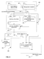
- FIG. 2 A block diagram of a time delay system according to an embodiment of the invention is shown in FIG. 2 .
- an accurate clock signal 280 is used as a calibration input signal.
- Accurate clock signal 280 can be generated, for example, by a crystal or resonator oscillator circuit (not shown).
- a start time delay signal 285 is used to initiate the time delay to be measured by the system.
- the system generates a time delay event signal 290 .
- the system includes an inaccurate clock circuit 200 that generates an inaccurate clock signal 215 .
- inaccurate clock circuit 200 has an inaccurate oscillator 205 that generates an inaccurate oscillator signal 207 .
- Inaccurate oscillator 205 may be, but is not limited to, a ring oscillator or relaxation oscillator, each of which is well known in the art. Such oscillators typically consume much less power, and are less accurate, in comparison with crystal- or resonator-based oscillator circuits.
- the frequency of inaccurate oscillator signal 207 must be less than the frequency of accurate clock signal 280 .
- the frequency of inaccurate oscillator signal 207 is about 0.1% to 10.0% of the frequency of accurate clock signal 280 .
- Frequency divider 210 then divides the frequency of inaccurate oscillator signal 207 to generate inaccurate clock signal 215 .
- frequency divider 210 would divide the frequency of the oscillator by 2, although other integer divisors may also be used.
- One reason for using frequency divider 210 would be to ensure that inaccurate clock signal 215 exhibits a 50% duty cycle.
- the signals generated by many inaccurate oscillators, some of which may be used for inaccurate oscillator 205 do not have a 50% duty cycle, which may affect the results of the calibration process, described below.
- Second, dividing inaccurate oscillator signal 207 by some small divisor would allow more cycles of accurate clock signal 280 to occur during a period of inaccurate clock signal 215 , thereby allowing a more accurate calibration of inaccurate clock signal 215 .
- frequency divider 210 can be removed, with inaccurate oscillator 205 generating is inaccurate clock signal 215 directly.
- Accurate clock signal 280 and inaccurate clock signal 215 are then used as input signals for a first clock counter circuit 220 , which counts the number of cycles of accurate clock signal 280 that occur during a predetermined portion of inaccurate clock signal 215 .
- a first digital counter 225 counts the number of cycles of accurate clock signal 280 each time inaccurate clock signal 215 , acting as an enable input for first digital counter 225 , is high, representing one-half of one period, as shown in FIG. 4 .
- other portions of inaccurate clock signal 215 such as an entire period, may be used to enable first digital counter 225 .
- Digital counter register 235 is loaded by way of a signal generated by a clock synchronization circuit 230 , which is a standard type of circuit used in integrated circuits, and is well known in the art.
- clock synchronization circuit 230 uses accurate clock signal 280 and inaccurate clock signal 215 to generate a load pulse after first digital counter 225 has been disabled so that the count value in first digital counter 225 is stable while it is being loaded into digital Counter register 235 , which is also shown in FIG. 4 .
- clock synchronization circuit 230 Other forms of clock synchronization circuit 230 are also possible.
- the load pulse could be generated at any time during which the count value of first digital counter 225 is stable.
- Digital processing unit 240 takes, as input, the output of digital counter register 235 to perform the calculation necessary to determine the number of cycles of inaccurate clock signal 215 that make up a desired time delay. In this case, the number of inaccurate clock signal cycles desired is
- N inacc (N inaccen ⁇ T delay )/(N accen ⁇ P acc ),
- N inacc is the number of cycles of inaccurate clock signal 215 representing the desired time delay
- N inaccen is the number of cycles of inaccurate clock signal 215 that are used to enable first digital counter 225
- T delay is the desired time delay (in seconds)
- N accen is the number of cycles of accurate clock signal 280 from digital counter register 235
- P acc is the period of the accurate clock signal 280 (in seconds).
- N inaccen is 0.5, since first digital counter 225 is enabled for one-half of a cycle of inaccurate clock signal 215 .
- N accen may be a recent value read from digital counter register 235 , or could be the result of some averaging algorithm utilizing several values acquired from digital counter register 235 .
- Digital processing unit 240 then passes the number of cycles of inaccurate clock signal 215 representing the desired time delay to a second counter circuit 260 that actually generates the time delay.
- Digital processing unit 240 may take several different forms, including, but not limited to, a microprocessor or digital signal processor IC with associated firmware for performing the required calculation, or a special purpose IC that performs the calculation in hardware. Such solutions may access first clock counter circuit 220 or second clock counter circuit 260 by either dedicated signal lines or general purpose data buses.
- Second clock counter circuit 260 counts the number of cycles of inaccurate clock signal 215 representing the desired time delay, whose value is stored by digital processing unit 240 in a maximum count register 265 .
- Start time delay signal 285 initiates or enables the counting in second digital counter 270 , which uses inaccurate clock signal 215 as a clock source.
- a digital comparator 275 compares the values of maximum count register 265 with that of second digital counter 270 to determine when the desired time period has elapsed. When the value of second digital counter 270 equals or surpasses the value of maximum count register 265 , digital comparator 275 generates time delay event signal 290 , indicating that the desired time delay has elapsed.
- second counter circuit 260 may be implemented by the use of a digital countdown counter 305 .
- Digital processing unit 240 sets the initial value of digital countdown counter 305 with the number of cycles of inaccurate clock signal 215 representing the desired time delay.
- start time delay signal 285 becomes active
- digital countdown counter 305 begins counting cycles of inaccurate clock signal 215 .
- time delay event signal 290 indicates that the desired time delay has elapsed.
- Another embodiment of the invention takes the form of a method of measuring a desired time delay, presented as a flow chart in FIG. 5 .
- an inaccurate clock signal is generated (step 500 ).
- the frequency of the inaccurate clock signal is lower than the frequency of an accurate clock signal used for calibration.
- the number of cycles of the accurate clock signal that occur during a predetermined portion of the inaccurate clock signal is then counted (step 510 ).
- a number of cycles of the inaccurate clock signal representing a desired time delay is then calculated using, the number of cycles of the inaccurate clock signal from the first counting step, the period of the accurate clock signal, the number of periods of the inaccurate clock signal in the predetermined portion from the first counting step, and the length of the desired time delay (step 520 ).
- the number of cycles of the inaccurate clock signal from the calculating step is then counted (step 530 ). Once the second counting step is completed, that fact is then indicated (step 540 ), thereby signifying that the desired time delay has elapsed.
- the frequency of the inaccurate clock signal is actually higher than that of the accurate clock signal being employed.
- the frequency of the inaccurate clock signal is typically, but not necessarily, 10 to 1000 times the frequency of the accurate clock signal.
- the number of cycles of inaccurate clock signal 215 are counted during a predetermined portion of accurate clock signal 280 using first digital counter 225 .
- clock synchronization circuit 230 uses inaccurate clock signal 215 , conditioned by accurate clock signal 280 , to generate a load pulse for digital counter register 235 once per cycle of accurate clock signal 280 that is synchronized with the waveform of inaccurate clock signal 215 .
- the graphs of FIG. 8 display an example of the signals involved with first clock counter circuit 220 in relation to the embodiments of FIG. 6 and FIG. 7 .
- N inacc (N inaccen ⁇ T delay )/(N accen ⁇ P acc ).
- N inaccen becomes the number of cycles of inaccurate clock signal 215 from digital counter register 235
- N accen becomes the number of cycles of accurate clock signal 280 that are used to enable first digital counter 225 . All other portions of the formula remain the same as discussed above.
- second clock counter circuit 260 of FIG. 7 and FIG. 8 is utilized in the same manner as the corresponding portions of FIG. 2 and FIG. 3 .
- an inaccurate clock signal is (generated (step 500 ), as also shown in FIG. 5 .
- the number of cycles of the inaccurate clock signal that occur during a predetermined portion of the accurate clock signal is then counted (step 910 ).
- a number of cycles of the inaccurate clock signal representing a desired time delay is then calculated using the number of cycles of the accurate clock signal from the first counting step, the period of the accurate clock signal, the number of periods of the inaccurate clock signal in the predetermined portion from the first counting step, and the length of the desired time delay (step 920 ).
- the number of cycles of the inaccurate clock signal from the calculating step are then counted (step 530 ), as in the embodiment of FIG. 5 .
Landscapes
- Pulse Circuits (AREA)
Priority Applications (4)
| Application Number | Priority Date | Filing Date | Title |
|---|---|---|---|
| US09/765,188 US6326825B1 (en) | 2001-01-18 | 2001-01-18 | Accurate time delay system and method utilizing an inaccurate oscillator |
| JP2001385522A JP2002261591A (ja) | 2001-01-18 | 2001-12-19 | 不正確な発振器を利用した正確な時間遅延システム及び方法 |
| DE10200698A DE10200698B4 (de) | 2001-01-18 | 2002-01-10 | Genaues Zeitverzögerungssystem und Verfahren unter Verwendung eines ungenauen Oszillators |
| SG200200299A SG115442A1 (en) | 2001-01-18 | 2002-01-16 | Accurate time delay system and method utilizing an inaccurate oscillator |
Applications Claiming Priority (1)
| Application Number | Priority Date | Filing Date | Title |
|---|---|---|---|
| US09/765,188 US6326825B1 (en) | 2001-01-18 | 2001-01-18 | Accurate time delay system and method utilizing an inaccurate oscillator |
Publications (1)
| Publication Number | Publication Date |
|---|---|
| US6326825B1 true US6326825B1 (en) | 2001-12-04 |
Family
ID=25072884
Family Applications (1)
| Application Number | Title | Priority Date | Filing Date |
|---|---|---|---|
| US09/765,188 Expired - Fee Related US6326825B1 (en) | 2001-01-18 | 2001-01-18 | Accurate time delay system and method utilizing an inaccurate oscillator |
Country Status (4)
| Country | Link |
|---|---|
| US (1) | US6326825B1 (enExample) |
| JP (1) | JP2002261591A (enExample) |
| DE (1) | DE10200698B4 (enExample) |
| SG (1) | SG115442A1 (enExample) |
Cited By (11)
| Publication number | Priority date | Publication date | Assignee | Title |
|---|---|---|---|---|
| EP1378998A1 (en) * | 2002-07-05 | 2004-01-07 | Stmicroelectronics SA | Method of operating a microcontroller chip having an internal RC oscillator, and microcontroller chip embodying the method |
| US20050221870A1 (en) * | 2004-04-06 | 2005-10-06 | Integration Associates Inc. | Method and circuit for determining a slow clock calibration factor |
| WO2006063485A1 (en) * | 2004-12-13 | 2006-06-22 | Apexone Microelectronics Ltd. | System and method for clock signal synchronization |
| US20060187866A1 (en) * | 2004-12-20 | 2006-08-24 | Sensicast Systems | Method for reporting and accumulating data in a wireless communication network |
| US20070194826A1 (en) * | 2006-02-17 | 2007-08-23 | Sen-Huang Tang | Circuit capable of self-correcting delay time and method thereof |
| US20110066868A1 (en) * | 2007-12-12 | 2011-03-17 | Lee Atkinson | Variably Delayed Wakeup Transition |
| US20110158031A1 (en) * | 2008-09-30 | 2011-06-30 | Ware Frederick A | Signal calibration methods and apparatuses |
| US20110302436A1 (en) * | 2010-06-04 | 2011-12-08 | Jeffrey Clark | System Wakeup on Wireless Network Messages |
| US20120112804A1 (en) * | 2010-11-09 | 2012-05-10 | Li Kuofeng | Calibration method and apparatus for clock signal and electronic device |
| US20140068303A1 (en) * | 2012-09-04 | 2014-03-06 | Intel Mobile Communications GmbH | Circuit arrangement and method for low power mode management |
| CN104679098A (zh) * | 2013-11-29 | 2015-06-03 | 上海华虹集成电路有限责任公司 | 微控制器时钟频率自动校准电路 |
Citations (3)
| Publication number | Priority date | Publication date | Assignee | Title |
|---|---|---|---|---|
| US4795984A (en) * | 1986-11-19 | 1989-01-03 | Schlumberger Systems & Services, Inc. | Multi-marker, multi-destination timing signal generator |
| US5815043A (en) * | 1997-02-13 | 1998-09-29 | Apple Computer, Inc. | Frequency controlled ring oscillator having by passable stages |
| US5969631A (en) * | 1996-06-14 | 1999-10-19 | Temic Telefunken Microelectronic Gmbh | Method and control system for the synchronized transmission of digital data |
Family Cites Families (3)
| Publication number | Priority date | Publication date | Assignee | Title |
|---|---|---|---|---|
| DE2928371C2 (de) * | 1979-07-13 | 1982-07-01 | Siemens AG, 1000 Berlin und 8000 München | Schaltungsanordnung zur Synchronisation von Zeitperioden zur Behandlung von Meßsignalen |
| DE19629869C2 (de) * | 1995-08-01 | 2003-02-13 | Schlumberger Technologies Inc | Verfahren und Vorrichtung zum Ausfluchten der relativen Phase von asychronen Taktsignalen |
| US6304979B1 (en) * | 1998-08-25 | 2001-10-16 | Infineon Technologies North America Corp. | Logic to enable/disable a clock generator in a secure way |
-
2001
- 2001-01-18 US US09/765,188 patent/US6326825B1/en not_active Expired - Fee Related
- 2001-12-19 JP JP2001385522A patent/JP2002261591A/ja active Pending
-
2002
- 2002-01-10 DE DE10200698A patent/DE10200698B4/de not_active Expired - Fee Related
- 2002-01-16 SG SG200200299A patent/SG115442A1/en unknown
Patent Citations (3)
| Publication number | Priority date | Publication date | Assignee | Title |
|---|---|---|---|---|
| US4795984A (en) * | 1986-11-19 | 1989-01-03 | Schlumberger Systems & Services, Inc. | Multi-marker, multi-destination timing signal generator |
| US5969631A (en) * | 1996-06-14 | 1999-10-19 | Temic Telefunken Microelectronic Gmbh | Method and control system for the synchronized transmission of digital data |
| US5815043A (en) * | 1997-02-13 | 1998-09-29 | Apple Computer, Inc. | Frequency controlled ring oscillator having by passable stages |
Cited By (21)
| Publication number | Priority date | Publication date | Assignee | Title |
|---|---|---|---|---|
| US20040068383A1 (en) * | 2002-07-05 | 2004-04-08 | Stmicroelectronics S.A. | Method of operating a microcontroller chip having an internal RC oscillator and microcontroller chip embodying the method |
| US6925402B2 (en) | 2002-07-05 | 2005-08-02 | Stmicroelectronics S.A. | Method of operating a microcontroller chip having an internal RC oscillator and microcontroller chip embodying the method |
| EP1378998A1 (en) * | 2002-07-05 | 2004-01-07 | Stmicroelectronics SA | Method of operating a microcontroller chip having an internal RC oscillator, and microcontroller chip embodying the method |
| US20050221870A1 (en) * | 2004-04-06 | 2005-10-06 | Integration Associates Inc. | Method and circuit for determining a slow clock calibration factor |
| EP1585223A1 (en) * | 2004-04-06 | 2005-10-12 | Integration Associates Inc. | Method and circuit for determining a slow clock calibration factor |
| WO2006063485A1 (en) * | 2004-12-13 | 2006-06-22 | Apexone Microelectronics Ltd. | System and method for clock signal synchronization |
| CN100547933C (zh) * | 2004-12-13 | 2009-10-07 | 埃派克森微电子有限公司 | 用于时钟信号同步的系统和方法 |
| US20060187866A1 (en) * | 2004-12-20 | 2006-08-24 | Sensicast Systems | Method for reporting and accumulating data in a wireless communication network |
| US8023441B2 (en) * | 2004-12-20 | 2011-09-20 | Sensicast Systems | Method for reporting and accumulating data in a wireless communication network |
| US20070194826A1 (en) * | 2006-02-17 | 2007-08-23 | Sen-Huang Tang | Circuit capable of self-correcting delay time and method thereof |
| US8677165B2 (en) * | 2007-12-12 | 2014-03-18 | Hewlett-Packard Development Company, L.P. | Variably delayed wakeup transition |
| US20110066868A1 (en) * | 2007-12-12 | 2011-03-17 | Lee Atkinson | Variably Delayed Wakeup Transition |
| US20110158031A1 (en) * | 2008-09-30 | 2011-06-30 | Ware Frederick A | Signal calibration methods and apparatuses |
| US8339895B2 (en) * | 2008-09-30 | 2012-12-25 | Rambus Inc. | Signal calibration methods and apparatuses |
| US8533506B2 (en) * | 2010-06-04 | 2013-09-10 | Lenovo (Singapore) Pte. Ltd. | System wakeup on wireless network messages |
| US20110302436A1 (en) * | 2010-06-04 | 2011-12-08 | Jeffrey Clark | System Wakeup on Wireless Network Messages |
| US20120112804A1 (en) * | 2010-11-09 | 2012-05-10 | Li Kuofeng | Calibration method and apparatus for clock signal and electronic device |
| US8766646B2 (en) * | 2010-11-09 | 2014-07-01 | Nuvoton Technology Corporation | Calibration method and apparatus for clock signal and electronic device |
| US20140068303A1 (en) * | 2012-09-04 | 2014-03-06 | Intel Mobile Communications GmbH | Circuit arrangement and method for low power mode management |
| US9021287B2 (en) * | 2012-09-04 | 2015-04-28 | Intel Mobile Communications GmbH | Circuit arrangement and method for low power mode management with delayable request |
| CN104679098A (zh) * | 2013-11-29 | 2015-06-03 | 上海华虹集成电路有限责任公司 | 微控制器时钟频率自动校准电路 |
Also Published As
| Publication number | Publication date |
|---|---|
| SG115442A1 (en) | 2005-10-28 |
| JP2002261591A (ja) | 2002-09-13 |
| DE10200698B4 (de) | 2004-01-22 |
| DE10200698A1 (de) | 2002-08-08 |
Similar Documents
| Publication | Publication Date | Title |
|---|---|---|
| US8823434B2 (en) | Clock correction circuit and clock correction method | |
| US5623234A (en) | Clock system | |
| CN109067394B (zh) | 片上时钟校准装置及校准方法 | |
| US6326825B1 (en) | Accurate time delay system and method utilizing an inaccurate oscillator | |
| EP0590607B1 (en) | Low-power baud rate generator | |
| US6084441A (en) | Apparatus for and method of processing data | |
| GB2521635A (en) | Improved low-power oscillator | |
| EP1585223B1 (en) | Method and circuit for determining a slow clock calibration factor | |
| JP6115715B2 (ja) | クロック生成装置、電子機器、移動体及びクロック生成方法 | |
| CN112953514A (zh) | 校准蓝牙时钟的方法和装置 | |
| US9966900B2 (en) | Apparatus for oscillator with improved precision and associated methods | |
| CN104601144A (zh) | 时钟生成装置、电子设备、移动体以及时钟生成方法 | |
| JP6319551B2 (ja) | クロック生成装置、電子機器、移動体及びクロック生成方法 | |
| US5410581A (en) | Apparatus and method for determining a time that a system's main power was inactive | |
| US6731708B1 (en) | Clock signal control device | |
| US7106118B2 (en) | Clock signal generator with low power comsumption function and method thereof | |
| TW202247609A (zh) | 時脈產生電路及其補償電路 | |
| US7315489B2 (en) | Method and apparatus for time measurement | |
| JP2000341092A (ja) | クロック信号発生回路及びそのクロック周波数調整方法 | |
| JP4036114B2 (ja) | クロック発生回路 | |
| US8630386B2 (en) | Clock recovery in a battery powered device | |
| CN119620581B (zh) | 双时钟驱动的高精度计时器及其计时方法 | |
| JP5037755B2 (ja) | 温度変化測定装置及びその方法 | |
| JPH09191249A (ja) | 周波数偏差補正方式 | |
| JPH0784666A (ja) | Cpuの間欠動作制御装置 |
Legal Events
| Date | Code | Title | Description |
|---|---|---|---|
| AS | Assignment |
Owner name: AGILENT TECHNOLOGIES, INC., CALIFORNIA Free format text: ASSIGNMENT OF ASSIGNORS INTEREST;ASSIGNOR:WALLEY, THOMAS M.;REEL/FRAME:011656/0374 Effective date: 20010312 |
|
| FEPP | Fee payment procedure |
Free format text: PAYOR NUMBER ASSIGNED (ORIGINAL EVENT CODE: ASPN); ENTITY STATUS OF PATENT OWNER: LARGE ENTITY |
|
| FPAY | Fee payment |
Year of fee payment: 4 |
|
| AS | Assignment |
Owner name: AVAGO TECHNOLOGIES GENERAL IP PTE. LTD., SINGAPORE Free format text: ASSIGNMENT OF ASSIGNORS INTEREST;ASSIGNOR:AGILENT TECHNOLOGIES, INC.;REEL/FRAME:017207/0020 Effective date: 20051201 |
|
| REMI | Maintenance fee reminder mailed | ||
| LAPS | Lapse for failure to pay maintenance fees | ||
| STCH | Information on status: patent discontinuation |
Free format text: PATENT EXPIRED DUE TO NONPAYMENT OF MAINTENANCE FEES UNDER 37 CFR 1.362 |
|
| FP | Lapsed due to failure to pay maintenance fee |
Effective date: 20091204 |
|
| AS | Assignment |
Owner name: AVAGO TECHNOLOGIES GENERAL IP (SINGAPORE) PTE. LTD., SINGAPORE Free format text: CORRECTIVE ASSIGNMENT TO CORRECT THE NAME OF THE ASSIGNEE PREVIOUSLY RECORDED ON REEL 017207 FRAME 0020. ASSIGNOR(S) HEREBY CONFIRMS THE ASSIGNMENT;ASSIGNOR:AGILENT TECHNOLOGIES, INC.;REEL/FRAME:038633/0001 Effective date: 20051201 Owner name: AVAGO TECHNOLOGIES GENERAL IP (SINGAPORE) PTE. LTD Free format text: CORRECTIVE ASSIGNMENT TO CORRECT THE NAME OF THE ASSIGNEE PREVIOUSLY RECORDED ON REEL 017207 FRAME 0020. ASSIGNOR(S) HEREBY CONFIRMS THE ASSIGNMENT;ASSIGNOR:AGILENT TECHNOLOGIES, INC.;REEL/FRAME:038633/0001 Effective date: 20051201 |