US6313261B1 - Polymer light emitting diode - Google Patents
Polymer light emitting diode Download PDFInfo
- Publication number
- US6313261B1 US6313261B1 US09/297,674 US29767499A US6313261B1 US 6313261 B1 US6313261 B1 US 6313261B1 US 29767499 A US29767499 A US 29767499A US 6313261 B1 US6313261 B1 US 6313261B1
- Authority
- US
- United States
- Prior art keywords
- semi
- polymer
- layer
- conducting
- electron
- Prior art date
- Legal status (The legal status is an assumption and is not a legal conclusion. Google has not performed a legal analysis and makes no representation as to the accuracy of the status listed.)
- Expired - Fee Related, expires
Links
Images


Classifications
-
- H—ELECTRICITY
- H10—SEMICONDUCTOR DEVICES; ELECTRIC SOLID-STATE DEVICES NOT OTHERWISE PROVIDED FOR
- H10K—ORGANIC ELECTRIC SOLID-STATE DEVICES
- H10K50/00—Organic light-emitting devices
- H10K50/10—OLEDs or polymer light-emitting diodes [PLED]
- H10K50/11—OLEDs or polymer light-emitting diodes [PLED] characterised by the electroluminescent [EL] layers
-
- Y—GENERAL TAGGING OF NEW TECHNOLOGICAL DEVELOPMENTS; GENERAL TAGGING OF CROSS-SECTIONAL TECHNOLOGIES SPANNING OVER SEVERAL SECTIONS OF THE IPC; TECHNICAL SUBJECTS COVERED BY FORMER USPC CROSS-REFERENCE ART COLLECTIONS [XRACs] AND DIGESTS
- Y10—TECHNICAL SUBJECTS COVERED BY FORMER USPC
- Y10S—TECHNICAL SUBJECTS COVERED BY FORMER USPC CROSS-REFERENCE ART COLLECTIONS [XRACs] AND DIGESTS
- Y10S428/00—Stock material or miscellaneous articles
- Y10S428/917—Electroluminescent
Definitions
- the present invention relates to novel polymer light emitting diodes, components and uses thereof, to a process for the production thereof and a method for light emission. More particularly the present invention relates to novel polymer light emitting diodes adapted for enhanced efficiency light emission, novel semi-conducting polymer components and uses thereof in displays and the like, to a process for the production thereof and a method for light emission.
- Illuminated displays have been in existence for some years now and are advantageous in a wide range of applications. Nevertheless shortcomings are continually being addressed by development of improved illumination techniques. For example cathode ray tubes are currently in operation in applications where their high power consumption, bulk and weight are acceptable. In less demanding applications liquid crystal displays are employed which operate by reflective rather than light emissive means. Such display technologies suffer problems of limited viewing angle, poor contrast and the like.
- Semi-conduction light emitting diodes employing conventional inorganic semi-conducting materials for light emission purpose. These provide an excellent viewing angle and contrast, but limited range of colours.
- Inorganic semi-conductors are generally crystalline materials leading to complicated manufacture and limited area of devices which may be made from them.
- LED's comprise two electrode layers, respectively a hole injecting layer and an electron injecting layer, typically comprising highly doped semi-conductor, metallic or ionic sheet layers, having an inorganic semi-conductor layer therebetween which serves to conduct holes and electrons to a region between both electrodes at which photon emission occurs.
- LEDs however are limited in the range of inorganic semi-conducting materials available and the wave length range of light in which they emit, commonly the infra-red range.
- a common arrangement employs a singe layer of polyparaphenylenevinylene (PPV) as semi-conducting polymer, which has been found to give an external quantum efficiency defined as number of photons emitted in the form of light detected outside the device, per electron flowing through the device of the order of 0.001% for an aluminium electron injecting contract layer, and of the order of 0.01% for a calcium electron injecting contact layer.
- PSV polyparaphenylenevinylene
- Light emission in organic conjugated polymeric materials may occur by the process of photo luminescence or electro luminescence, as indicated in FIG. 1 and FIG. 2 .
- photo luminescence may take place by photo excitation of a polymer, without need for charge conduction, for example photoluminescence has observed for PPV, with emission of light at a longer wavelength (sometimes referred to as the Stokes shift) than that absorbed.
- Luminescence efficiency by radiative decay of the singlet excition can be reduced by a variety of competing non-radiative decay processes.
- Electroluminescence is elcetrically inducded by light emission. In contract to photoluminescence, it results from respective electron and hole injection causing excitation and negative and positive polaron formation. Coincidence of a negative and positive polaron in a luminescent material causes singlet exciton formation with emission of light. Reduced luminescence efficiency may take place as mentioned for photoluminescence, by migration of polarons to a “trap” or “quench” whereby energy is lost-radiatively, or as a result of the proximity of electrodes.
- polymeric LED's Despite the poor efficiency of polymeric LED's, they have highly significant potential advantages in terms of their processability and ability to be deposited over large areas as high quality, robust and/or flexible thin films, for example enabling construction of flexible, very large area LED's, inherent radiative decay properties, emission range covering the whole range of the spectrum, and chemical tailoring of polymer materials to realise desired properties, to name but a few.
- a device adapted for light emission comprising a plurality of component layers of which a first outer layer is adapted for electron injection, a second opposing outer layers is adapted for “hole” injection, and one or more intermediate layers arranged therebetween are adapted for charge semi-conduction wherein the intermediate layer(s) comprise at least one semi-conducting polymer adapted for electron transport and/or hole blocking, and at least one semi-conducting polymer adapted for hole transport and/or electron blocking wherein the at least one semi-conducting polymer adapted for electron transport and/or hole blocking comprises polymer selected from a nitrogen and/or sulphur containing polymer which is partially or substantially conjugated.
- the at least one semi-conducting polymer adapted for electron transport and/or hole blocking is selected from a conjugated polycyclic in which at least one nitrogen and/or sulphur is a heteroatom comprised within a conjugated heterocyclic system.
- the invention provides a mechanism which resembles the balanced injection and balanced transport of electrons and holes.
- the device is characterised by an attractive external quantum efficiency, as hereinbefore defined, and an attractive brightness, measured as Cd/m 2 .
- the device comprises intermediate layer(s) comprised of one or more semi-conducting polymers, the type, purity, concentration and layer thickness whereof are adapted for efficient electron and hole transport in relative manner.
- the device comprises semi-conducting polymer of chemical and physical nature adapted for electroluminescence, by polaron formation, migration, coincidence and decay in manner that at least one photon of radiation emission is emitted from the device per 400 electrons injected into the device.
- the migration and coincidence of electrons and “holes” may be manipulated, whereby a boundary region for coincidence thereof may be positioned relative to the first and second outer layers in an emissive region in manner to provide enhanced brightness and/or external quantum efficiency.
- the positioning of the boundary region is a function of the respective degrees of transport of electrons and holes within the intermediate layer(s).
- a device of the invention is characterised by an external quantum efficiency of at least 0.1%, more preferably at least 0.2%, most preferably at least 2.0%.
- a device of the invention is characterised by a brightness of at least 100 Cd/m 2 , more preferably at least 500 Cd/m 2 , most preferably at least 2000 Cd/m 2 .
- component layer is to a substantially uniform discrete layer of a material, the properties of which are suited to the function of the layer. Accordingly it will be apparent that individual layers are distinguished by nature of component material, which may comprise a plurality of chemical entities present as a physical or chemical mixture.
- component layers are provided with substantially continuous interface therebetween by suitable means as known in the art, for example by bonding, contact curing and the like with use of co-extrusion, spin or dip coating, electro vacuum deposition process and the like.
- Reference herein to semi-conducting layer(s) is to component layers of electron and “hole” transporting materials respectively, present as component layers. These materials favour the transport of negative and positive charge respectively, are also known an n-type and p-type materials.
- Reference herein to electrons and holes is to negative positive charge carriers respectively, as known in the art, also known as negative and positive polarons.
- a junction comprises a substantially continuous planar region through the device of the invention, substantially co-planar with the component layers thereof.
- the junction is preferably of uniform thickness.
- the junction may coincide with the interface between component layers or may be comprised within one, or bridging two, component layers.
- the junction coincides with or bridges the interface between two semi-conducting layers which are of different charge semi-conduction nature i.e., one of which is electron transporting and the other of which is hole transporting. It is a particular advantage that the position of the junction, which represents the emissive region, in a particular layer or on the interface between two layers provides a means of controlling emission colour, for example the characteristic emissive colour of one of two layers, or of both layers in the form of two colour emission.
- each conducting layer provides uniform and efficient transport, for the entire layer thickness thereof.
- This provides a novel means for improving the efficiency and brightness of devices made from existing luminescent polymers, or from novel improved efficiency luminescent polymers alike. Accordingly there is provided according to the present invention a device as hereinbefore defined wherein the junction position may be influenced with resulting property change, and means for influencing the junction position.
- At least one charge semi-conduction layer, or a component thereof is capable of light emission by luminescence.
- the emissive layer(s) or component thereof are substantially coincident with the junction of coincidence of charge carriers. More preferably the or each charge semi-conduction layer is substantially emissive.
- the junction position may be influenced by any suitable means.
- the junction position is a function of the nature of semi-conducting polymers employed and of the respective thickness of semi-conducting layers employed. It will be appreciated that by appropriate selection of these parameters the respective transport of positive and negative charge carriers (polarons) through the semi-conducting layers may be controlled in manner that sufficient charge coincides at a junction as hereinbefore defined to achieve the external efficiency as hereinbefore defined.
- the ratio of thickness may be selected by those skilled in the art, for example by calculation having regard to whether the respective semi-conductors are emissive or non-emissive and the degree of emission, i.e., the quantum efficiency, thereof.
- the ratio of thickness are in the region of 0.1-10, more preferably 0.15-9, most preferably 0.3-5, in each case the least thickness layer representing the least efficient charge carrier transporter.
- the ratio of thickness may also suitably be determined by experiment, by means of monitoring the brightness and efficiency of electro-luminescence for different ratios of thickness of component semi-conductor layers. For example, by determination of (degree of) luminescence achieved with a device having one semi-conducting layer under test, in combination with a second control semi-conducting layer, only one of each which semi-conducting layers is luminescent, chemical and physical variations of the polymer under test may be made.
- Total semi-conducting layer thickness is suitable selected in the range of from 10 to 200 nm, preferably from 30 to 150 nm. Two low a thickness risks entering the range of errors of polymer thickness, whereby short-circuiting may occur at “bald” regions or “pinholes” having substantially no polymer. Excessive thickness requires high voltage operation with resultant power efficiency. Total layer thickness may therefore be selected according to requirements of robustness, cost and quality.
- a device as hereinbefore defined may comprise one or more electron transporting and one or more hole transporting layers, preferably comprises one electron transporting and one hole transporting layer.
- a component layer as hereinbefore defined adapted for electron injection is suitable comprised of any suitable electron injecting material for example as known in the art, preferably comprises any suitable metal, alloy or semi-conductor such as calcium, magnesium, gold, aluminium and the like optionally as an admixture with suitable agents.
- the present invention enables the selection of aluminium as electron injection layer and surprisingly give efficient devices.
- a component layer as hereinbefore defined adapted for hole injection is suitably comprised of any suitable hole injecting material for example as known in the art, preferably comprises any suitable metal, alloy or semi-conductor such as indium tin oxide (ITO), tin oxide or other transparent conductor, PEDOT, polyaniline or like polymer, gold and the like, optionally as an admixture with suitable agents.
- ITO indium tin oxide
- PEDOT polyaniline or like polymer
- gold and the like optionally as an admixture with suitable agents.
- a component layer as hereinbefore defined adapted for electron transport is suitably comprised of any n-type conducting material for example as known in the art but comprises at least one nitrogen and/or sulphur containing polymer as hereinbefore defined which optionally partly or substantially conjugated, preferably comprises polypyridine (Ppy), polyalkylpyridines, polypyrimidines, polyalkylpyrimidines, polythiazoles, polyalkylthiazoles, derivatives such as fluorinated derivatives, analogues and functional equivalents thereof.
- Such material may be present in pure form, doped or undoped, protonated or unprotonated, oxidised or reduced or together with suitable agents, for example may be doped by grafting or mixing for property enhancement.
- a component layer as hereinbefore defined adapted for hole transport is suitably comprised of any known p-type conducting material for example as known in the art, but which comprise any suitable conjugated organic molecule, dye or dye-doped polymer system, preferably comprises polyparaphenylenevinylene (PPV), poly(2-methoxy-5-(2′-ethyl-hexyloxy)-p-phenylenevinylene) (MEH-PPV), cyano PPV, poly(p-phenylene), poly(alkylthiophene), derivatives, monomers, oligomers, analogues and functional equivalents thereof.
- PPV polyparaphenylenevinylene
- MEH-PPV poly(2-methoxy-5-(2′-ethyl-hexyloxy)-p-phenylenevinylene)
- MEH-PPV poly(2-methoxy-5-(2′-ethyl-hexyloxy)-p-phenylenevinylene)
- semi-conducting polymers are substantially uncontaminated by electron and/or “hole” quenching or trapping species which may be reduce their transmission efficiency.
- electron transport and/or hole blocking semi-conducting polymer preferably polypyridine is most advantageously employed in high purity, preferably in substantially cation free form, wherein cations deriving from the polymerisation reagent employed or the preparation of such reagent are substantially absent as synthetic residue from the polymer structure.
- the semi-conducting polymer is prepared by the reaction of precursor monomers and/or oligomers in the presence of a zero-valent chelating metal reagent and a salt of a cation, wherein the zero-valent chelating metal is present in stoichiometric excess to the cation.
- Component materials as hereinbefore defined advantageously are characterised by a life time suited to the purpose for which the device is adapted.
- aluminium is characterised by a particular beneficial life time.
- Polymers are advantageously resistant to photo-oxidation.
- a device as hereinbefore defined may comprise any further supporting, sealing or protective layers and the like.
- a device as hereinbefore defined comprises a transparent rigid or flexible support layer such as quartz or glass or suitable synthetic equivalent such as polymeric substrates on which the device is constructed or onto which the constructed device is transferred, whereby the integrity and uniformity thereof is preserved.
- a support layer may be used during the construction of the device, onto which either outer layer may be deposited as desired, and intermediate and opposing layers subsequently applied, and a second layer to be used during use applied to either outer layer as desired.
- a semi-conducting polymer in a device as hereinbefore defined.
- the nitrogen and/or sulphur containing, optionally partially or substantially conjugated polymers as hereinbefore defined are characterised by excellent electron transporting properties, given n-type conduction and improved external quantum efficiency when used as electron transporting layer of an LED or a device as hereinbefore defined.
- the efficiency thereof may be enhanced by enhancing the synthetic quality thereof.
- a semi-conducting polymer for use as an n-type conducting layer in a device as hereinbefore defined comprises polypyridine, more preferably comprises polypyridine which is substantially free of quenches or traps for charge carriers.
- a substantially pure polymerisation reagent for example a zero-valent nickel polymerisation reagent substantially free of salts of cations for example Zn from ZnCl 2 .
- the polypyridine obtained by this process is found to provide excellent purity product polymer.
- an electron transporting and/or hole blocking polymer for use as an n-type semi-conductor, optionally in a device as hereinbefore defined, comprising a nitrogen and/or sulphur containing polymeric material as hereinbefore defined which is preferably substantially free of charge carrier quenching or trapping moieties. More preferably an electron transporting polymeric material is substantially free of materials capable of trapping negative charge or quenching luminescence.
- a highly efficient electron or hole transporting polymeric material may be used in desired purity or thickness to enable the variation of relative degree of electron and hole transport in a semi-conducting device.
- a device as hereinbefore defined as a light emitting display (LED) of any desired surface area and for portable or fixed purpose.
- a display may comprise a single continuous device or a mosaic of devices depending on the size and nature thereof. It is a particular advantage of the invention that a device of the invention is characterised by high quality for any application.
- a device is used for display purposes, such as electroluminescent TV or computer screens, back lighting of liquid crystal displays such as in watches and the like, very large area displays such as public information boards in airports and the like, small displays such as for household electrical goods including calculators, washing machines and the like, flexible displays, head-up (virtual reality) displays for training, entertainment purposes and the like, for example for aircraft pilot, road user training and the like; for improved efficiency applications such as for lighting of large areas, preferably by means of panelled low intensity (low brightness) wall or ceiling lighting in place of a plurality of independent lights, lighting powered by a battery source such as car brake lights, lighting in constant use such as traffic lights, warning and or road signs which may be optionally flashing or otherwise active, visible or near infra red security lighting, pulse mode camera flash applications, and the like; and for advanced technology applications such as solid state conjugated polymers lasers, micro cavity LED's enabling modification of wave length and the like; and for application in clothing for safety or fashion purpose.
- liquid crystal displays such as in watches and
- a nitrogen and/or sulphur containing polymer as hereinbefore defined as an n-type semi-conductor for example for use in a semi-conducting electronic device, such as a transistor, solar cell, a photodiode, diode, triode and the like.
- an efficient electron transporting and/or hole blocking polymer as a component of a semi-conductor or semi-conducting device as hereinbefore defined. It is a particular advantage that the present invention provides a new range of efficient electron transporting polymers, the advantageous properties of which were heretofore unknown, by means of providing the polymer substantially free of materials capable of trapping negative charge or quenching luminescence as hereinbefore defined.
- a device may suitably be produced by any technique as known in the art.
- a device as hereinbefore defined is producing by providing a first support layer of desired dimensions and coating this with successive component layers as hereinbefore defined.
- metallic component layers are deposited by electrolytic or reactive means or by evaporation.
- a semi-conducting polymer as hereinbefore defined is coated in a layer as hereinbefore defined by means of spin coating or dip-coating of the polymer or a precursor thereof, and optionally curing, or by equivalent high precision technique such as electrochemical deposition or evaporation for providing a polymer film.
- a device as hereinbefore defined comprises or is adapted to be associated with means for mounting and operation thereof in known manner. It is a particular advantage that devices of the invention may be viewed from a large range of angles simplifying their mounting, and greatly improving their visibility. It is a further advantage that the devices may be used to provide a rapid response for pulse operation. Devices may be used in AC or DC operation, with the hereinbefore mentioned advantages of power consumption supply and brightness.
- a method for the operation of light emitting diode as hereinbefore defined Suitably a light emitting diode as hereinbefore defined is operated in known manner, by applying voltage, causing a current to flow through the device.
- a device as hereinbefore defined may be conveniently and reliably operated by virtue of the high external quantum efficiency thereof.
- FIG. 3 illustrates the construction of an LED device as known in the art
- FIG. 4 illustrates an LED comprising a device according to the invention.
- FIG. 5 illustrates a display screen comprising the device of FIG. 2 .
- FIG. 6 illustrates the current voltage—light output characteristic of the device of FIG. 4 .
- FIGS. 7 and 8 illustrate the light output—current characteristic of devices of FIG. 4 and devices of FIG. 3 .
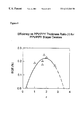
- FIG. 9 illustrated the efficiency—thickness ratio characteristic of a bilayer device of the invention.
- FIG. 3 The construction of a typical electrode/polymer/electrode device is illustrated in FIG. 3.
- a high work function electrode such an indium-tin oxide (ITO) (4.6 eV), deposited on a glass substrate ( 1 ) serves as the anode ( 2 ) and is semi-transparent at thickness of 7-10 nm.
- the precursor of polymer, such as PPV is deposited as a thin film on the electrode and, converted into the conjugated material, thereby providing semi-conducting polymer layer ( 3 ).
- a low work function metal, such as calcium or aluminium is evaporated onto the polymer surface ( 3 ) by a vacuum metal vapour deposition, and serves as the cathode ( 4 ).
- Electrical contacts are provided ( 5 , 6 ) linking the anode ( 2 ) and cathode ( 4 ) to a suitable power supply (not shown).
- a suitable power supply not shown.
- high field strengths (of the order of 10 6 V/cm) are required, although with the use of thin films of the order of 100 nm, the forward bias voltage of the device can be as low as a few volts.
- FIG. 4 is shown the construction of an electrode/polymer/electrode device according to the invention.
- the device comprises the same component parts as indicated for FIG. 3, optionally comprising a plurality of semi-conducting polymer layers.
- FIG. 4 shows a layer ( 3 ), such as PPV as described with reference to FIG. 3, and additionally a semi-conducting polymer layer ( 7 ), such as polypyridine (Ppy) directly deposited from a solution of Ppy as the polymer, as a thin film on the pre-prepared PPV layer ( 3 ).
- the respective thickness of layer ( 3 ) and ( 7 ) is as hereinbefore defined.
- first illustrative purpose layer ( 3 ) is of the order 120 nm and layer ( 7 ) is the order of up to 40 nm, thereby having a thickness ratio of 3.
- second illustrative purpose layer ( 3 ) is of the order of 90 nm and layer ( 7 ) is of the order of 50 nm, thereby having a thickness ratio of 1.8.
- the device of FIG. 4 may be operated at field strengths of the order of 10 6 V/cm in order to achieve charge injection.
- the forward bias voltage of the device may be of the order of 2-20 V depending on layer thickness.
- FIG. 5 is illustrated an outdoor display screen which comprises the device of FIG. 4 of which the layers are continuous throughout the cross-section area of the screen ( 8 ), or as repeating sub-units of continuous layers (indicated as dotted lines).
- the front panel of the display comprises a glass substrate layer ( 1 ) as hereinbefore described for FIG. 4, or a suitable transparent material having mechanical properties adapted to resist deformation and fracture, and having a refractive index suited for the designed light emission properties.
- the device of FIG. 4 having a thickness ratio of 1.8 providing an external quantum efficiency of greater than or equal to 0.2% and brightness of the order of 1100 Cd/m 2 in continuous wave operation, or brighter in pulsed operation may be visible from a distance, depending on the colour of visible light emission, detail and clarity of the image or message being portrayed. This compares with an inferior range for a similar image or message portrayed on a screen constructed of the device of FIG. 3, having an external quantum efficiency of the order of 0.01% or less and brightness of the order of tens of Cd/m 2 .
- a glass or quartz surface of thickness of the order of 1 mm, coated with ITO to a thickness of 80 nm+/ ⁇ 15 nm was used as the support for component layers of the device as hereinbefore defined, commercially available (Balzers 30 Ohms per square).
- PPV precursor polymer comprising the tetrahydrothiophenium (THT) leaving group as a solution in methanol was spin coated to a thickness of 100 nm onto the glass/ITO substrate, and converted to PPV by heating at 250° C. for ten hours under dynamic vacuum.
- a Ppy layer comprising the polymer in solution prepared by dissolving Ppy powder in 97% formic acid was spin coated directly onto the PPV layer to form a homogeneous thin film requiring no thermal conversion, and of a thickness of up to 100 nm+/ ⁇ 5 nm.
- the cathode comprising aluminium was coated onto the Ppy layer by evaporation at a pressure of 5 ⁇ 10 ⁇ 6 mbar, at a rate of 0.1-0.5 nms ⁇ 1 .
- Ppy powder used in the preparation of the device was prepared by conventional technique but modified with use of a nickel catalyst, in controlled fashion.
- the product polymer obtained by this novel modified process was substantially uncontaminated by cations of salt components employed in the catalyst preparation, such as zinc, which may operate as a trap or quench in disadvantageous manner as hereinbefore defined.
- the purity of the polymer may be selected as appropriate, for example the photoluminescence quantum yield gives one measure of the purity of the material.
- the device prepared according to Example 1 was connected to a suitable power supply by electrical contacts placed at the ITO anode and the Al cathode.
- the device was operated at a turn-on voltage of 12V and current-voltage and current-intensity measurements carried out. From the data obtained and indicated in FIGS. 6 and 7, the external quantum efficiency was determined.
- a device according to the invention was prepared using the method of Example 1 but employing MEH-PPV as the emissive layer, prepared from the appropriate precursor.
- Example 3 The device prepared according to Example 3 was connected and operated as described in Example 2. The results are shown in Table 1.
- Comparative devices were prepared using known techniques, and as hereinbefore defined, comprising the device of FIG. 1, and the device of FIG. 2 having inefficient layer thickness ratio.
- the process of Example 2 was employed and the same measurements were conducted as described for Example 2 and external efficiency data were determined.
- layer thickness is a function of the materials employed, the techniques for preparation and the skill and apparatus available, however layer thickness of spin coated polymers obtained directly from solution as hereinbefore defined are generally prepared to an accuracy of +/ ⁇ 5 nm. Deviations in thickness across a device as hereinbefore defined may contribute to inhomogeneity of the electric field in the device whereby some reduction in efficiency, uniformity and lifetime may be observed.
- the bilayer device is also much more efficient than a single layer device with a calcium contract (5 th row)
- bilayer MEH-PPV devices (6 th row) are a factor of 4 more efficient than similar devices without the polypyridine layer (7 th row).
- the results demonstrate a substantial improvement in efficiency with both PPV and MEH-PPV as the emissive layers, which may be expected to apply also with a wide range of existing (or future) luminescent materials. Without being limited to this theory the magnitude of increase efficiency is thought to be proportional to the barrier to electron injection for example in MEH-PPV.
- FIG. 7 shows the intensity-current density characteristics of bilayer and single layer diodes.
- the solid line shows the behaviour of a bilayer PPV/PPY diode of thickness 140 nm and a PPY:PPY thickness ratio of 1.8.
- the dashed line shows the results for a 120 nm thick PPV device with calcium electrodes.
- the dotted line shows the results for a 140 nm thick PPV device with aluminium contracts.
- the external quantum efficiency of each diode is proportional to the slope of each curve.
- the bilayer diode has an efficiency of 0.25%, much higher than the efficiency of 0.01% for the PPV/Ca diode and 0.004% for the PPV/Al diode.
- the lower FIG. 7 shows the current density-field (line) and intensity-field (symbols) characteristics of the bilayer diode.
- the current density shows typical diode field dependence.
- the FIG. 8 shows intensity-current density characteristics of bilayer and single layer MEH-PPV/PPY and MEH-PPV diodes.
- the bilayer diode has an efficiency of 0.04%, much higher than the single layer diode efficiency of 0.009%.
- the FIG. 9 shows efficiency vs thickness ratio characteristics for bilayer diodes.
- the figure shows that maximum efficiencies are achieved for an optimum ratio of thickness, which coincides with balanced electron and hole transport which is thought to coincide at a junction, within the layer capable of light emission by luminescence.
Landscapes
- Physics & Mathematics (AREA)
- Optics & Photonics (AREA)
- Electroluminescent Light Sources (AREA)
- Led Device Packages (AREA)
- Led Devices (AREA)
Applications Claiming Priority (3)
| Application Number | Priority Date | Filing Date | Title |
|---|---|---|---|
| GBGB9623204.6A GB9623204D0 (en) | 1996-11-07 | 1996-11-07 | Polymer light emitting diode |
| GB9623204 | 1996-11-07 | ||
| PCT/GB1997/003019 WO1998020565A1 (en) | 1996-11-07 | 1997-11-07 | Polymer light emitting diode |
Publications (1)
| Publication Number | Publication Date |
|---|---|
| US6313261B1 true US6313261B1 (en) | 2001-11-06 |
Family
ID=10802592
Family Applications (1)
| Application Number | Title | Priority Date | Filing Date |
|---|---|---|---|
| US09/297,674 Expired - Fee Related US6313261B1 (en) | 1996-11-07 | 1997-11-07 | Polymer light emitting diode |
Country Status (9)
| Country | Link |
|---|---|
| US (1) | US6313261B1 (zh) |
| EP (1) | EP0954883A1 (zh) |
| JP (1) | JP2001503908A (zh) |
| CN (1) | CN1236489A (zh) |
| AU (1) | AU725250B2 (zh) |
| CA (1) | CA2270609A1 (zh) |
| GB (1) | GB9623204D0 (zh) |
| NZ (1) | NZ335365A (zh) |
| WO (1) | WO1998020565A1 (zh) |
Cited By (17)
| Publication number | Priority date | Publication date | Assignee | Title |
|---|---|---|---|---|
| US20010043164A1 (en) * | 1999-04-27 | 2001-11-22 | Gregory B. Thagard | Clothing with image display |
| US6597012B2 (en) * | 2001-05-02 | 2003-07-22 | Junji Kido | Organic electroluminescent device |
| GB2396252A (en) * | 2002-10-01 | 2004-06-16 | Steven Leftly | Textile light system |
| US20040176048A1 (en) * | 2003-02-20 | 2004-09-09 | Gunnar Klinghult | Keypad lighting using polymer light emitting devices |
| US20050014019A1 (en) * | 2003-07-18 | 2005-01-20 | Ying Wang | Method of selecting a charge transport and/or anti-quenching material |
| WO2005022958A1 (de) * | 2003-09-01 | 2005-03-10 | Gertrud Balmer | Elektrolumineszenten leuchtsysteme integriert mit, lichtmesser, erschütterungs oder druckmelder und steuerungselektronik mit el-folien-treiber |
| US20050125874A1 (en) * | 2003-01-08 | 2005-06-16 | Devore Sandra B. | Garment and garment accessories having luminescent accents and fabrication method therefor |
| US20050276910A1 (en) * | 2004-06-09 | 2005-12-15 | Osram Opto Semiconductors Gmbh | Post processing of films to improve film quality |
| US20060118901A1 (en) * | 2004-11-17 | 2006-06-08 | Plextronics, Inc. | Heteroatomic regioregular poly(3-substitutedthiophenes) as thin film conductors in diodes whcih are not light emitting or photovoltaic |
| US20060180812A1 (en) * | 2005-02-15 | 2006-08-17 | Semiconductor Energy Laboratory Co., Ltd. | Light emitting element and light emitting device |
| GB2424512A (en) * | 2005-03-22 | 2006-09-27 | Riso Nat Lab | Method of forming photovoltaic device |
| US20070072000A1 (en) * | 2003-10-24 | 2007-03-29 | National Institute Of Advanced Industrial Science And Technology | Organic electroluminescent element and manufacturing method thereof |
| US20090072715A1 (en) * | 2005-03-28 | 2009-03-19 | Konica Minolta Holdings, Inc. | Organic electroluminescent element, display and illuminator |
| US20110030789A1 (en) * | 2008-02-18 | 2011-02-10 | The Technical University Of Denmark | Air stable photovoltaic device |
| US20130009131A1 (en) * | 2008-04-03 | 2013-01-10 | Kazlas Peter T | Device including quantum dots |
| US10333090B2 (en) | 2008-04-03 | 2019-06-25 | Samsung Research America, Inc. | Light-emitting device including quantum dots |
| US20190207135A1 (en) * | 2018-01-03 | 2019-07-04 | Boe Technology Group Co., Ltd. | Display panel and display device |
Families Citing this family (9)
| Publication number | Priority date | Publication date | Assignee | Title |
|---|---|---|---|---|
| AT410729B (de) * | 2000-04-27 | 2003-07-25 | Qsel Quantum Solar Energy Linz | Photovoltaische zelle mit einer photoaktiven schicht aus zwei molekularen organischen komponenten |
| WO2002012212A1 (de) | 2000-08-07 | 2002-02-14 | Siemens Aktiengesellschaft | Di(het)arylaminothiazol-derivate und ihre verwendung in organischen lichtemittierenden dioden (oleds) und organischen photovoltaischen bauelemente |
| DE10051369A1 (de) * | 2000-10-17 | 2002-05-02 | Fraunhofer Ges Forschung | Polymeres Schaltelement |
| CN100346496C (zh) * | 2002-09-13 | 2007-10-31 | 友达光电股份有限公司 | 有机电致发光元件 |
| CN101414667B (zh) * | 2003-04-23 | 2010-06-09 | 柯尼卡美能达控股株式会社 | 有机电致发光元件和显示装置 |
| TW200621940A (en) * | 2003-08-20 | 2006-07-01 | Tdk Corp | Organic EL device and method for manufacturing same |
| CN100490206C (zh) * | 2003-12-25 | 2009-05-20 | 华南理工大学 | 有机/高分子发光二极管 |
| EP1809077A2 (en) * | 2004-09-22 | 2007-07-18 | Japan Science and Technology Agency | Organic electroluminescent element |
| TWI393283B (zh) | 2008-12-04 | 2013-04-11 | Univ Nat Chiao Tung | 有機光電元件 |
Citations (4)
| Publication number | Priority date | Publication date | Assignee | Title |
|---|---|---|---|---|
| US5247196A (en) * | 1990-03-30 | 1993-09-21 | Mitsubishi Denki Kabushiki Kaisha | Semiconductor memory device including capacitor having stacked structure and manufacturing method thereof |
| JPH06346051A (ja) | 1993-06-11 | 1994-12-20 | Osaka Gas Co Ltd | 有機エレクトロルミネッセンス素子 |
| DE19627071A1 (de) | 1996-07-05 | 1998-01-08 | Bayer Ag | Elektrolumineszierende Anordnungen |
| US5723873A (en) * | 1994-03-03 | 1998-03-03 | Yang; Yang | Bilayer composite electrodes for diodes |
-
1996
- 1996-11-07 GB GBGB9623204.6A patent/GB9623204D0/en active Pending
-
1997
- 1997-11-07 NZ NZ335365A patent/NZ335365A/xx unknown
- 1997-11-07 CN CN97199523A patent/CN1236489A/zh active Pending
- 1997-11-07 AU AU49544/97A patent/AU725250B2/en not_active Ceased
- 1997-11-07 JP JP52114298A patent/JP2001503908A/ja active Pending
- 1997-11-07 US US09/297,674 patent/US6313261B1/en not_active Expired - Fee Related
- 1997-11-07 CA CA002270609A patent/CA2270609A1/en not_active Abandoned
- 1997-11-07 EP EP97912301A patent/EP0954883A1/en not_active Withdrawn
- 1997-11-07 WO PCT/GB1997/003019 patent/WO1998020565A1/en not_active Application Discontinuation
Patent Citations (4)
| Publication number | Priority date | Publication date | Assignee | Title |
|---|---|---|---|---|
| US5247196A (en) * | 1990-03-30 | 1993-09-21 | Mitsubishi Denki Kabushiki Kaisha | Semiconductor memory device including capacitor having stacked structure and manufacturing method thereof |
| JPH06346051A (ja) | 1993-06-11 | 1994-12-20 | Osaka Gas Co Ltd | 有機エレクトロルミネッセンス素子 |
| US5723873A (en) * | 1994-03-03 | 1998-03-03 | Yang; Yang | Bilayer composite electrodes for diodes |
| DE19627071A1 (de) | 1996-07-05 | 1998-01-08 | Bayer Ag | Elektrolumineszierende Anordnungen |
Non-Patent Citations (6)
| Title |
|---|
| "Blue Light Emitting Organic Electroluminescent Device" Applied Phys. Lett. 56(9) 799-801 (1990) Adachi et al.* |
| Dailey, S., "Polypyridine as an Efficient Electron-Transporting Polymer for Light-Emitting Diodes", Dept. Of Physics, Univ. of Durham, U.K. |
| Gebler, D.D. et al, "Blue Electroluminescent Devices Based On Soluble Poly(p-pyridine)", Journal of Applied Physics, vol. 78, No. 6, Sep. 15, 1995. |
| Holmes, A.B. et al, "Photoluminescence and Electroluminescence in Conjugated Polymeric Systems", Synthetic Metals, 55-57 (1993), pp. 4031-4040. |
| Onoda, M., Light Emitting Diodes Using n-Type Conducting Polymer: Poly (p-pyridyl vinylene), Journal of Applied Physics, vol. 78, No. 2, Jul. 15, 1995, pp. 1327-1333. |
| Weaver, M.S., "Recent Progress in Polymers for Electroluminesence: Microcavity Devices and Electron Transport Polymers", Thin Solid Films 273 (1996), pp. 39-47. |
Cited By (28)
| Publication number | Priority date | Publication date | Assignee | Title |
|---|---|---|---|---|
| US20010043164A1 (en) * | 1999-04-27 | 2001-11-22 | Gregory B. Thagard | Clothing with image display |
| US6597012B2 (en) * | 2001-05-02 | 2003-07-22 | Junji Kido | Organic electroluminescent device |
| GB2396252A (en) * | 2002-10-01 | 2004-06-16 | Steven Leftly | Textile light system |
| US20050125874A1 (en) * | 2003-01-08 | 2005-06-16 | Devore Sandra B. | Garment and garment accessories having luminescent accents and fabrication method therefor |
| US7379720B2 (en) | 2003-02-20 | 2008-05-27 | Sony Ericsson Mobile Communications Ab | Keypad lighting using polymer light emitting devices |
| US20040176048A1 (en) * | 2003-02-20 | 2004-09-09 | Gunnar Klinghult | Keypad lighting using polymer light emitting devices |
| US7612306B2 (en) | 2003-02-20 | 2009-11-03 | Sony Ericsson Mobile Communications Ab | Keypad lighting using polymer light emitting devices |
| US20080173526A1 (en) * | 2003-02-20 | 2008-07-24 | Sony Ericsson Mobile Communication Ab | Keypad lighting using polymer light emitting devices |
| US20050014019A1 (en) * | 2003-07-18 | 2005-01-20 | Ying Wang | Method of selecting a charge transport and/or anti-quenching material |
| WO2005022958A1 (de) * | 2003-09-01 | 2005-03-10 | Gertrud Balmer | Elektrolumineszenten leuchtsysteme integriert mit, lichtmesser, erschütterungs oder druckmelder und steuerungselektronik mit el-folien-treiber |
| US20110081478A1 (en) * | 2003-10-24 | 2011-04-07 | National Institute Of Advanced Industrial Science And Technology | Organic electroluminescent element and manufacturing method thereof |
| US20070072000A1 (en) * | 2003-10-24 | 2007-03-29 | National Institute Of Advanced Industrial Science And Technology | Organic electroluminescent element and manufacturing method thereof |
| US20050276910A1 (en) * | 2004-06-09 | 2005-12-15 | Osram Opto Semiconductors Gmbh | Post processing of films to improve film quality |
| US20060118901A1 (en) * | 2004-11-17 | 2006-06-08 | Plextronics, Inc. | Heteroatomic regioregular poly(3-substitutedthiophenes) as thin film conductors in diodes whcih are not light emitting or photovoltaic |
| US7321133B2 (en) | 2004-11-17 | 2008-01-22 | Plextronics, Inc. | Heteroatomic regioregular poly(3-substitutedthiophenes) as thin film conductors in diodes which are not light emitting or photovoltaic |
| US9530968B2 (en) * | 2005-02-15 | 2016-12-27 | Semiconductor Energy Laboratory Co., Ltd. | Light emitting element and light emitting device |
| US20060180812A1 (en) * | 2005-02-15 | 2006-08-17 | Semiconductor Energy Laboratory Co., Ltd. | Light emitting element and light emitting device |
| GB2424512A (en) * | 2005-03-22 | 2006-09-27 | Riso Nat Lab | Method of forming photovoltaic device |
| US20090072715A1 (en) * | 2005-03-28 | 2009-03-19 | Konica Minolta Holdings, Inc. | Organic electroluminescent element, display and illuminator |
| US8703300B2 (en) * | 2005-03-28 | 2014-04-22 | Konica Minolta Holdings, Inc. | Organic electroluminescent element, display and illuminator |
| US20110030789A1 (en) * | 2008-02-18 | 2011-02-10 | The Technical University Of Denmark | Air stable photovoltaic device |
| US20130009131A1 (en) * | 2008-04-03 | 2013-01-10 | Kazlas Peter T | Device including quantum dots |
| US9525148B2 (en) * | 2008-04-03 | 2016-12-20 | Qd Vision, Inc. | Device including quantum dots |
| US9755172B2 (en) | 2008-04-03 | 2017-09-05 | Qd Vision, Inc. | Device including quantum dots |
| US10164205B2 (en) | 2008-04-03 | 2018-12-25 | Samsung Research America, Inc. | Device including quantum dots |
| US10333090B2 (en) | 2008-04-03 | 2019-06-25 | Samsung Research America, Inc. | Light-emitting device including quantum dots |
| US11005058B2 (en) | 2008-04-03 | 2021-05-11 | Samsung Research America, Inc. | Light-emitting device including quantum dots |
| US20190207135A1 (en) * | 2018-01-03 | 2019-07-04 | Boe Technology Group Co., Ltd. | Display panel and display device |
Also Published As
| Publication number | Publication date |
|---|---|
| JP2001503908A (ja) | 2001-03-21 |
| CN1236489A (zh) | 1999-11-24 |
| EP0954883A1 (en) | 1999-11-10 |
| WO1998020565A1 (en) | 1998-05-14 |
| GB9623204D0 (en) | 1997-01-08 |
| CA2270609A1 (en) | 1998-05-14 |
| AU725250B2 (en) | 2000-10-12 |
| AU4954497A (en) | 1998-05-29 |
| NZ335365A (en) | 2000-10-27 |
Similar Documents
| Publication | Publication Date | Title |
|---|---|---|
| US6313261B1 (en) | Polymer light emitting diode | |
| US6414431B1 (en) | Thin film electrode for planar organic light-emitting devices and method for its production | |
| Bernius et al. | Progress with light‐emitting polymers | |
| Friend et al. | Polymer diodes | |
| US6252253B1 (en) | Patterned light emitting diode devices | |
| KR101201826B1 (ko) | 유기발광소자 및 표시장치 | |
| US20060145599A1 (en) | OLEDs with phosphors | |
| Braun et al. | Electroluminescence from light-emitting diodes fabricated from conducting polymers | |
| JP2002117970A (ja) | 屋外用エレクトロルミネセンスディスプレイ装置 | |
| Yu et al. | Planar light-emitting devices fabricated with luminescent electrochemical polyblends | |
| EP1171544B1 (en) | Electroluminescent materials | |
| US10243160B2 (en) | Organic light emitting device, manufacturing method thereof and display apparatus | |
| Tiwari et al. | Recent progress in organic light-emitting diodes | |
| JPH0794278A (ja) | 有機薄膜発光素子 | |
| JPH05114487A (ja) | 有機薄膜発光素子 | |
| Kobayashi | BiOLED with DNA/Conducting Polymer Complex as Active Layer. | |
| JPH02251429A (ja) | 透明導電性フィルム | |
| WO2000029779A1 (en) | Process for generating luminescence emissions from polymer solutions, gels, and liquid polymers in a compact cell configuration, and device employing same | |
| JPH02251428A (ja) | 透明導電性フィルム | |
| Ficke et al. | The bright future of organic LEDs | |
| US11302886B2 (en) | Perovskite light-emitting device, preparation method thereof, and display | |
| US7408185B2 (en) | Organic light emitting device and display using the same | |
| Khaty | A Review-the Development in Organic Light Emitting Diodes (Oleds) the Future of Displays | |
| Karasz | Electroluminescence from ionic polymers doped with cationic dyes | |
| KR100252777B1 (ko) | 백색광유기전기발광소자의제조방법 |
Legal Events
| Date | Code | Title | Description |
|---|---|---|---|
| AS | Assignment |
Owner name: DURHAM, UNIVERSITY OF, UNITED KINGDOM Free format text: ASSIGNMENT OF ASSIGNORS INTEREST;ASSIGNORS:MONKMAN, ANDREW PAUL;SAMUEL, IFOR DAVID WILLLIAM;REBOURT, EYMARD GABRIEL FRANCOIS JOSEPH;AND OTHERS;REEL/FRAME:010296/0017;SIGNING DATES FROM 19990715 TO 19990818 |
|
| REMI | Maintenance fee reminder mailed | ||
| LAPS | Lapse for failure to pay maintenance fees | ||
| STCH | Information on status: patent discontinuation |
Free format text: PATENT EXPIRED DUE TO NONPAYMENT OF MAINTENANCE FEES UNDER 37 CFR 1.362 |
|
| FP | Lapsed due to failure to pay maintenance fee |
Effective date: 20051106 |