US6049656A - Method of mounting an integrated circuit on a printed circuit board - Google Patents
Method of mounting an integrated circuit on a printed circuit board Download PDFInfo
- Publication number
- US6049656A US6049656A US08/979,311 US97931197A US6049656A US 6049656 A US6049656 A US 6049656A US 97931197 A US97931197 A US 97931197A US 6049656 A US6049656 A US 6049656A
- Authority
- US
- United States
- Prior art keywords
- pcb
- integrated circuit
- leads
- semiconductor chip
- holding block
- Prior art date
- Legal status (The legal status is an assumption and is not a legal conclusion. Google has not performed a legal analysis and makes no representation as to the accuracy of the status listed.)
- Expired - Lifetime
Links
Images


Classifications
-
- B—PERFORMING OPERATIONS; TRANSPORTING
- B23—MACHINE TOOLS; METAL-WORKING NOT OTHERWISE PROVIDED FOR
- B23K—SOLDERING OR UNSOLDERING; WELDING; CLADDING OR PLATING BY SOLDERING OR WELDING; CUTTING BY APPLYING HEAT LOCALLY, e.g. FLAME CUTTING; WORKING BY LASER BEAM
- B23K1/00—Soldering, e.g. brazing, or unsoldering
- B23K1/005—Soldering by means of radiant energy
-
- H—ELECTRICITY
- H05—ELECTRIC TECHNIQUES NOT OTHERWISE PROVIDED FOR
- H05K—PRINTED CIRCUITS; CASINGS OR CONSTRUCTIONAL DETAILS OF ELECTRIC APPARATUS; MANUFACTURE OF ASSEMBLAGES OF ELECTRICAL COMPONENTS
- H05K3/00—Apparatus or processes for manufacturing printed circuits
- H05K3/30—Assembling printed circuits with electric components, e.g. with resistor
- H05K3/32—Assembling printed circuits with electric components, e.g. with resistor electrically connecting electric components or wires to printed circuits
- H05K3/34—Assembling printed circuits with electric components, e.g. with resistor electrically connecting electric components or wires to printed circuits by soldering
- H05K3/341—Surface mounted components
- H05K3/3421—Leaded components
-
- H—ELECTRICITY
- H05—ELECTRIC TECHNIQUES NOT OTHERWISE PROVIDED FOR
- H05K—PRINTED CIRCUITS; CASINGS OR CONSTRUCTIONAL DETAILS OF ELECTRIC APPARATUS; MANUFACTURE OF ASSEMBLAGES OF ELECTRICAL COMPONENTS
- H05K3/00—Apparatus or processes for manufacturing printed circuits
- H05K3/30—Assembling printed circuits with electric components, e.g. with resistor
- H05K3/32—Assembling printed circuits with electric components, e.g. with resistor electrically connecting electric components or wires to printed circuits
- H05K3/34—Assembling printed circuits with electric components, e.g. with resistor electrically connecting electric components or wires to printed circuits by soldering
- H05K3/3489—Composition of fluxes; Methods of application thereof; Other methods of activating the contact surfaces
-
- B—PERFORMING OPERATIONS; TRANSPORTING
- B23—MACHINE TOOLS; METAL-WORKING NOT OTHERWISE PROVIDED FOR
- B23K—SOLDERING OR UNSOLDERING; WELDING; CLADDING OR PLATING BY SOLDERING OR WELDING; CUTTING BY APPLYING HEAT LOCALLY, e.g. FLAME CUTTING; WORKING BY LASER BEAM
- B23K2101/00—Articles made by soldering, welding or cutting
- B23K2101/36—Electric or electronic devices
- B23K2101/40—Semiconductor devices
-
- H—ELECTRICITY
- H05—ELECTRIC TECHNIQUES NOT OTHERWISE PROVIDED FOR
- H05K—PRINTED CIRCUITS; CASINGS OR CONSTRUCTIONAL DETAILS OF ELECTRIC APPARATUS; MANUFACTURE OF ASSEMBLAGES OF ELECTRICAL COMPONENTS
- H05K2201/00—Indexing scheme relating to printed circuits covered by H05K1/00
- H05K2201/10—Details of components or other objects attached to or integrated in a printed circuit board
- H05K2201/10431—Details of mounted components
- H05K2201/10606—Permanent holder for component or auxiliary PCB mounted on a PCB
-
- H—ELECTRICITY
- H05—ELECTRIC TECHNIQUES NOT OTHERWISE PROVIDED FOR
- H05K—PRINTED CIRCUITS; CASINGS OR CONSTRUCTIONAL DETAILS OF ELECTRIC APPARATUS; MANUFACTURE OF ASSEMBLAGES OF ELECTRICAL COMPONENTS
- H05K2201/00—Indexing scheme relating to printed circuits covered by H05K1/00
- H05K2201/10—Details of components or other objects attached to or integrated in a printed circuit board
- H05K2201/10613—Details of electrical connections of non-printed components, e.g. special leads
- H05K2201/10621—Components characterised by their electrical contacts
- H05K2201/10681—Tape Carrier Package [TCP]; Flexible sheet connector
-
- H—ELECTRICITY
- H05—ELECTRIC TECHNIQUES NOT OTHERWISE PROVIDED FOR
- H05K—PRINTED CIRCUITS; CASINGS OR CONSTRUCTIONAL DETAILS OF ELECTRIC APPARATUS; MANUFACTURE OF ASSEMBLAGES OF ELECTRICAL COMPONENTS
- H05K2201/00—Indexing scheme relating to printed circuits covered by H05K1/00
- H05K2201/10—Details of components or other objects attached to or integrated in a printed circuit board
- H05K2201/10613—Details of electrical connections of non-printed components, e.g. special leads
- H05K2201/10621—Components characterised by their electrical contacts
- H05K2201/10689—Leaded Integrated Circuit [IC] package, e.g. dual-in-line [DIL]
-
- H—ELECTRICITY
- H05—ELECTRIC TECHNIQUES NOT OTHERWISE PROVIDED FOR
- H05K—PRINTED CIRCUITS; CASINGS OR CONSTRUCTIONAL DETAILS OF ELECTRIC APPARATUS; MANUFACTURE OF ASSEMBLAGES OF ELECTRICAL COMPONENTS
- H05K2203/00—Indexing scheme relating to apparatus or processes for manufacturing printed circuits covered by H05K3/00
- H05K2203/01—Tools for processing; Objects used during processing
- H05K2203/0147—Carriers and holders
- H05K2203/0165—Holder for holding a Printed Circuit Board [PCB] during processing, e.g. during screen printing
-
- H—ELECTRICITY
- H05—ELECTRIC TECHNIQUES NOT OTHERWISE PROVIDED FOR
- H05K—PRINTED CIRCUITS; CASINGS OR CONSTRUCTIONAL DETAILS OF ELECTRIC APPARATUS; MANUFACTURE OF ASSEMBLAGES OF ELECTRICAL COMPONENTS
- H05K2203/00—Indexing scheme relating to apparatus or processes for manufacturing printed circuits covered by H05K3/00
- H05K2203/04—Soldering or other types of metallurgic bonding
- H05K2203/0485—Tacky flux, e.g. for adhering components during mounting
-
- H—ELECTRICITY
- H05—ELECTRIC TECHNIQUES NOT OTHERWISE PROVIDED FOR
- H05K—PRINTED CIRCUITS; CASINGS OR CONSTRUCTIONAL DETAILS OF ELECTRIC APPARATUS; MANUFACTURE OF ASSEMBLAGES OF ELECTRICAL COMPONENTS
- H05K2203/00—Indexing scheme relating to apparatus or processes for manufacturing printed circuits covered by H05K3/00
- H05K2203/10—Using electric, magnetic and electromagnetic fields; Using laser light
- H05K2203/104—Using magnetic force, e.g. to align particles or for a temporary connection during processing
-
- H—ELECTRICITY
- H05—ELECTRIC TECHNIQUES NOT OTHERWISE PROVIDED FOR
- H05K—PRINTED CIRCUITS; CASINGS OR CONSTRUCTIONAL DETAILS OF ELECTRIC APPARATUS; MANUFACTURE OF ASSEMBLAGES OF ELECTRICAL COMPONENTS
- H05K2203/00—Indexing scheme relating to apparatus or processes for manufacturing printed circuits covered by H05K3/00
- H05K2203/10—Using electric, magnetic and electromagnetic fields; Using laser light
- H05K2203/107—Using laser light
-
- H—ELECTRICITY
- H05—ELECTRIC TECHNIQUES NOT OTHERWISE PROVIDED FOR
- H05K—PRINTED CIRCUITS; CASINGS OR CONSTRUCTIONAL DETAILS OF ELECTRIC APPARATUS; MANUFACTURE OF ASSEMBLAGES OF ELECTRICAL COMPONENTS
- H05K2203/00—Indexing scheme relating to apparatus or processes for manufacturing printed circuits covered by H05K3/00
- H05K2203/30—Details of processes not otherwise provided for in H05K2203/01 - H05K2203/17
- H05K2203/304—Protecting a component during manufacturing
-
- H—ELECTRICITY
- H05—ELECTRIC TECHNIQUES NOT OTHERWISE PROVIDED FOR
- H05K—PRINTED CIRCUITS; CASINGS OR CONSTRUCTIONAL DETAILS OF ELECTRIC APPARATUS; MANUFACTURE OF ASSEMBLAGES OF ELECTRICAL COMPONENTS
- H05K3/00—Apparatus or processes for manufacturing printed circuits
- H05K3/30—Assembling printed circuits with electric components, e.g. with resistor
- H05K3/32—Assembling printed circuits with electric components, e.g. with resistor electrically connecting electric components or wires to printed circuits
- H05K3/34—Assembling printed circuits with electric components, e.g. with resistor electrically connecting electric components or wires to printed circuits by soldering
- H05K3/3494—Heating methods for reflowing of solder
-
- Y—GENERAL TAGGING OF NEW TECHNOLOGICAL DEVELOPMENTS; GENERAL TAGGING OF CROSS-SECTIONAL TECHNOLOGIES SPANNING OVER SEVERAL SECTIONS OF THE IPC; TECHNICAL SUBJECTS COVERED BY FORMER USPC CROSS-REFERENCE ART COLLECTIONS [XRACs] AND DIGESTS
- Y02—TECHNOLOGIES OR APPLICATIONS FOR MITIGATION OR ADAPTATION AGAINST CLIMATE CHANGE
- Y02P—CLIMATE CHANGE MITIGATION TECHNOLOGIES IN THE PRODUCTION OR PROCESSING OF GOODS
- Y02P70/00—Climate change mitigation technologies in the production process for final industrial or consumer products
- Y02P70/50—Manufacturing or production processes characterised by the final manufactured product
Definitions
- the present invention relates to a method of mounting an integrated circuit having a plurality of leads on a printed circuit board, and more particularly, to a method of mounting an integrated circuit of a tape carrier package (TCP) type on a printed circuit board (PCB).
- TCP tape carrier package
- PCB printed circuit board
- TM Pentium
- TM Pentium
- a Pentium (TM) processor of the TCP type will be explained as an integrated circuit in an embodiment of a method for mounting the integrated circuit on the PCB of the present invention.
- an integrated circuit of the TCP type is a very small compartment which includes 320 pins and has a spacing of 0.2 mm between the leads. Moreover, the integrated circuit of the TCP type is formed without a wire bonding which is used in the conventional semiconductor chip. As a result, as the size of the circuit is small, and the size of the printed circuit board can be smaller.
- a semiconductor chip for performing a practical function of the integrated circuit is located at the center of a polyimide film.
- the semiconductor chip is attached to the polyimide film and it is slightly thicker than the polyimide film.
- Leads from the semiconductor chip are formed on the back side of the polyimide film with a pattern shape thereby maintaining the insulation between the leads and protecting them from external shock.
- Slots are formed at positions spaced apart from the edges of the polyimide film so as to face each edge of the semiconductor chip and a portion of the leads are exposed.
- An integrated circuit of the TCP type with this structure is supplied from the manufacturer with a plastic carrier for protection, and is mounted on the PCB.
- the PCB on which the operation is finished in the previous process is transported by a transporting guide rail to be provided, the PCB is fixed and a flux is evenly spread over the lead patterns on the PCB corresponding to the positions where the leads of the integrated circuit are to be soldered.
- the leads of the integrated circuit are aligned to correspond accurately to the lead patterns on the PCB.
- a hot bar at a high temperature presses the leads of the integrated circuit located on the lead patterns of the PCB so as to solder the leads of the integrated circuit on the lead patterns. Since solder has previously been coated on the lead patterns of the integrated circuit on the PCB during the previous process, it is possible to perform the soldering operation.
- the integrated circuit leads are cut to a predetermined size by a cutting and forming tool suitable to lead patterns on the PCB.
- the cutting and forming tool is lowered on the integrated circuit and cuts the polyimide film which is located at the other side of the semiconductor chip centered around the slot. As a result, the array of the leads is properly performed after the cutting operation is finished.
- the leads can be misaligned when the hot bar presses the leads of the integrated circuit at a high temperature during the soldering step.
- shorts between adjacent leads can frequently occur and as the hot bar presses the leads directly, it is possible to damage a thin lead.
- the life of the leads can be reduced though they are soldered and shorts between the leads can occur.
- the PCB employing the earlier mounting method typically has a groove having a rectangular shape similar to the size of the semiconductor chip of the integrated circuit located at the position for mounting the integrated circuit.
- the groove is used to mount a heat sink which emits heat generated when the integrated circuit operates. Since the backside of the semiconductor chip of the integrated circuit protrudes slightly from the polyimide film, the backside of the semiconductor chip and the beat sink are connected by attaching conductive adhesive pads to the protruding part of the semiconductor chip and one end of the heat sink.
- the rectangular groove acts as a spacer for the connection. It takes a considerable amount of time however, to attach the heat sink and the operation is very difficult.
- any foreign substance on a PCB is removed and a flux is spread over a lead pattern formed on the PCB.
- the leads of the integrated circuit are positioned after being aligned on the lead patterns of the PCB on which the flux is spread.
- the soldered PCB and the holding block are cooled.
- a conductive bond can be spread over the part where the semiconductor chip of the integrated circuit is placed on the PCB, before the flux is spread.
- the conductive bond is spread over an area which is 60% of the size of the semiconductor chip.
- the spread conductive bond is simultaneously spread over the surface of the PCB and over the back side of the PCB through a via hole which is formed to penetrate the PCB.
- the heat sink is attached by using the conductive bond spread on the back side of the PCB.
- the flux is spread using a nozzle or a stamp in which the lead pattern is carved.
- the PCB Before aligning the integrated circuit, the PCB can be fixed using a magnet fixing jig and the PCB is fixed by the combination of a magnetic substance attached to the holding block and the magnet fixing jig.
- a recognition mark formed on the PCB is used to align the integrated circuit on the PCB, and thus, the aligning operation becomes easy.
- a xenon (Xe) lamp is used as a source for generating the optical beam. After adhering the integrated circuit by the holding block, the leads of the integrated circuit are aligned on the lead pattern of the PCB. As a result, when radiating the optical beam, the part of the semiconductor chip of the integrated circuit can be shielded from the optical beam.
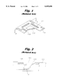
- FIG. 1 is a partial cross-sectional perspective view showing an integrated circuit of the TCP type
- FIG. 2 is a sectional view illustrating the integrated circuit which is soldered after it is cut along the line I-I' of FIG. 1;
- FIG. 3 is a sectional view illustrating a method for attaching a heat sink to the integrated circuit
- FIG. 4 is a block diagram illustrating a device for mounting the integrated circuit, according to the present invention.
- FIG. 5 is a flowchart illustrating a sequential process for mounting the integrated circuit of the present invention
- FIGS. 6A to 6C are views illustrating the process for mounting the integrated circuit, according to the present invention.
- FIG. 7A is a perspective view of a holding block
- FIG. 7B is a perspective view which is partly cut illustrating the holding block being located on the integrated circuit
- FIG. 8A is a perspective view of a magnet fixing jig
- FIG. 8B is a sectional view of the magnet fixing jig on which the PCB is mounted.
- FIG. 9 is an illustrative view showing an example in which the heat sink is attached to the PCB on which the integrated circuit is mounted.
- FIG. 1 is a perspective view which is partly cut to show an integrated circuit of the TCP type.
- a semiconductor chip 100 for performing a practical function of the integrated circuit is located at the center of a polyimide film 103.
- the semiconductor chip 100 is attached to the polyimide film 103 and it is slightly thicker than the polyimide film 103.
- Leads 102 from the semiconductor chip 100 are formed on the back side of the polyimide film 103 with a pattern shape, thereby maintaining the insulation between the leads 102 and protecting them from external shock.
- slots 106 are formed at positions spaced apart from the edges on the polyimide film 103 to face each edge of the semiconductor chip 100, and some parts of the leads are exposed.
- the integrated circuit of the TCP type having the above-described structure, as supplied from the manufacturer, is received in a plastic carrier for protection and is mounted on the PCB.
- the PCB on which the operation is finished in the previous process is transported by a transporting guide rail to be provided, the PCB is fixed and a flux is evenly spread over the lead patterns on the PCB corresponding to the positions where the leads of the integrated circuit are to be soldered, using a brush.
- the leads of the integrated circuit are aligned to correspond accurately to the lead patterns on the PCB.
- a hot bar at a high temperature presses the leads of the integrated circuit located on the lead patterns on the PCB, and thereby the leads of the integrated circuit are soldered on the lead patterns on the PCB.
- the solder has been previously coated on the lead patterns of the integrated circuit on the PCB during the previous process, it is possible to perform the soldering operation.
- the PCB on which the integrated circuit is mounted is unloaded onto a tray.
- the process for cutting and forming the leads of the integrated circuit is explained as follows. After loading the integrated circuit which is received by the plastic carrier in the tray into the cutting and forming unit, the integrated circuit leads are cut to a predetermined size by a cutting and forming tool suitable to the lead patterns on the PCB.
- the cutting and forming tool is lowered on the integrated circuit which is received in the plastic carrier transported to the cutting and forming unit, and cut the integrated circuit along the line I-I' of FIG. 1.
- the cutting is performed by including a polyimide film 103, which is located at the other side of the semiconductor chip 100 centering around a slot 106.
- the array of the leads is properly performed after the cutting operation is finished.
- the cut leads are formed in a predetermined shape directly by the cutting and forming tool and have a proper shape suitable to the lead pattern on the PCB.
- the leads can be misaligned when the hot bar presses the leads of the integrated circuit at a high temperature during the soldering step. As a result, shorts between adjacent leads can frequently occur. As the hot bar presses the leads directly, it is possible to damage the lead having a thin thickness. Moreover, the life of the leads can be reduced though they are soldered, and shorts between the leads can occur.
- the PCB employing the earlier mounting method has a groove 116 having a rectangular shape similar to the size of the semiconductor chip 100 of the integrated circuit at the position for mounting the integrated circuit.
- the groove 116 is used to mount a heat sink 130 which emits heat generated when the integrated circuit operates.
- the back side of the semiconductor chip 100 of the integrated circuit protrudes slightly from the polyimide film 130
- the back side of the semiconductor chip 100 and the heat sink 130 are connected by attaching conductive adhesive pads 113 and 113' to the protruding part of the semiconductor chip 100 and one end of the heat sink 130.
- the rectangular groove 116 acts as a spacer for the connection. I have found however, it takes much time to attach the heat sink and the operation is very difficult.
- a device for mounting which is employed in the process of the present invention, may be constructed with: a loading unit 10 for loading an array PCB finished the operation at the previous process to the working plate; a dispenser unit 20 for spreading a conductive bond over a part corresponding to a chip of the integrated circuit on the PCB which is loaded; a cutting and forming unit 30 for cutting the integrated circuit supplied by being received in a plastic carrier into a predetermined size and forming leads; a mounting unit 40 for spreading a flux on the lead pattern of the integrated circuit on the PCB on which the conductive bond is spread and aligning the leads of the integrated circuit which are formed so as to be aligned to the pattern of the integrated circuit on the PCB; a soldering unit 50 for soldering the integrated circuit positioned on the PCB with an optical beam of a Xenon lamp; and a cooling unit for cooling the soldered PCB.
- the process for mounting the integrated circuit of the present invention will be explained, with reference to the drawings.
- contaminating substances stuck to the PCB 110 supplied to the loading unit 10 which is transported from the previous process are blown away using an air gun (Step 210).
- the PCB 110 supplied as a preferred embodiment of the present invention is an array PCB in which four PCBs each having a same size are combined in a one array.
- the array PCB 110 is transported to the next working position, and it is fixed on a magnet fixing jig 120, as shown in FIGS. 8A and 8B.
- the magnet fixing jig 120 includes a flat board plate 122 having a rectangular shape and supporting legs 124 formed at each edge of the flat board plate 122.
- On the flat board plate 122 four rectangular grooves 128 are formed corresponding to the array PCB 110.
- the rectangular groove 128 faces a pattern unit of the PCB 110.
- magnets 126 for fixing the holding block are buried in a predetermined depth at the edges of the rectangular groove 128.
- a pair of recognition marks 115 are formed at the edges of the array PCB 110 in a diagonal direction.
- the recognition marks 115 are supposed to be reference marks when aligning the holding block 150 on the PCB 110.
- the conductive bond 114 is spread over a predetermined area from the central part of the region where the semiconductor chip 100 of the integrated circuit is disposed on the PCB 110 by a dispenser (not illustrated) located in the dispenser unit 20 (Step 220). At this time, the conductive bond 114 is preferably spread over the part corresponding to 60% of the size of the semiconductor chip 100.
- a predetermined number of via holes 118 are formed at the part where the conductive bond 114 of the PCB 110 is spread. Some of the spread conductive bond 114 penetrates the via hole 118 and is spread over the back side of the PCB 110.
- the conductive bond 114' spread on the back side of the PCB 110 enables the heat generated when the semiconductor chip 100 of the integrated circuit operates to be emitted by attaching the heat sink 130 at the back side of the PCB 110. In other words, it is unnecessary to provide a rectangular groove in the PCB 110 to attach the heat sink 130. As the heat sink 130 can be attached to the PCB 110 only by using the spread conductive bond 114' on the back side, the operation can easily be performed.
- the spread conductive bond 114 compensates for the interval between the semiconductor chip 100 of the integrated circuit and the PCB 110 only by the leads 102 of the integrated circuit which are bent at the forming process, the stability in mounting the integrated circuit can be ensured.
- the conductive bond 114 is serially spread in a similar way.
- the solid-powdered flux is evenly spread on the lead pattern on the PCB corresponding to the part where the leads 102 of the integrated circuit are to be soldered using a nozzle (step 230).
- the flux can be spread at a time by imprinting on the lead pattern of the PCB 110 after dipping a stamp in which the shape of the lead pattern of the integrated circuit is calved into the flux.
- the aforesaid method can spread the flux evenly and rapidly, in comparison with the conventional process using a brush.
- the solid powdered flux is used as a lubricant for soldering smoothly in the soldering step which will be the next step.
- the array PCB 110 on which the flux received on the magnet fixing jig 120 is spread is transported along the transporting guide rail and then transported to the mounting unit 40 on which a camera is mounted so as to monitor the lead pattern on the PCB 110 by magnifying the lead pattern.
- the integrated circuit which is received in the plastic carrier and then supplied is cut and formed in a predetermined size suitable to the lead pattern on the PCB 110 (Step 310).
- the cutting and forming tool 160 lowers to around the outer end of the slot 106 and cuts a plurality of leads 102 at a time.
- the polyimide film 103 which is located outside of the slot 106 is removed.
- the leads which are cut are formed as a shape each having a predetermined curvature so that they can properly be attached to the PCB 110.
- the integrated circuit After adhering the integrated circuit which finishes cutting and forming operation to the holding block 150, the integrated circuit is moved on the lead pattern of the PCB 110 so as to be aligned (Step 240).
- the holding block 150 is adhered by a vacuum pump and it is transported to the position where the integrated circuit which is cut and formed is located.
- the holding block 150 has a rectangular shape having a predetermined thickness corresponding to the shape of the semiconductor chip 100 of the integrated circuit which is cut and formed.
- a predetermined number of holes 154 are included so that the integrated circuit located inside of the holding block 150 can be adhered to the holding block 150 using the vacuum pump provided inside of the mounting device.
- a rectangular groove (not illustrated) corresponding to the size of the semiconductor chip 100 of the integrated circuit is formed at the back side of the holding block 150 so as to adhere stably to the integrated circuit.
- a supporting part 152 having a predetermined length is established.
- magnetic substances 156 each having a predetermined thickness are attached to each lower part of the supporting parts 152. The magnetic substances are contacted to the magnets 126 located at the magnet fixing jig 120 to fix the holding block 150 in the aligning step.
- the alignment can be performed automatically or manually using the image regarding the position of the PCB and the integrated circuit transmitted from the camera.
- the position of the PCB 110 fixed at the magnet fixing jig 120 is recognized using the recognition mark 115 of the PCB 110.
- the leads 102 of the integrated circuit which are formed are accurately aligned to face the upper part of the lead patterns 330 of the PCB 110.
- the integrated circuit is lowered on the lead pattern 330 of the PCB 110 together with the holding block 150 by manipulating the vacuum pump. As shown in FIG.
- the holding block 150 and the PCB 110 on which the integrated circuit is located are transported to the soldering unit 50.
- the soldering operation is performed at a high temperature of 300° C. (step 250). At this time, the optical beam radiates evenly into the overall lead patterns 330 on the PCB 110 which is to be soldered for an even soldering.
- the lead is hardly damaged and shorts can be prevented.
- the PCB 110 which finishes soldering is transported to the cooling unit 60, and the holding block 150 and the PCB 110 having a high temperature due to the soldering are cooled (step 260). After that, the holding block 150 is lifted from the PCB 110 by the vacuum pump and is unloaded (step 270), and the remaining three PCBs of the array PCB 110 repeatedly perform the above-described process.
- the mounting method of the present invention adopt the soldering operation using the optical beam, it is possible to prevent shorts and a poor contact generated by the earlier method.
- the quality of soldering is enhanced and the lead is not pressured when soldering, the reliability of the integrated circuit after mounting is also enhanced.
- the operational time can be reduced.
- the conductive bond in advance over the part where the integrated circuit on the PCB is to be mounted, the gap between the semiconductor chip and the PCB caused by the formed lead when locating the integrated circuit on the PCB can be avoided, thereby enhancing the stability in mounting the integrated circuit. Moreover, it is unnecessary to form a rectangular groove in the PCB to attach the heat sink, and the heat sink is attached to the PCB by using the conductive bond which is spread over the back side, thereby performing the operation without difficulty.
Abstract
Description
Claims (20)
Applications Claiming Priority (2)
| Application Number | Priority Date | Filing Date | Title |
|---|---|---|---|
| KR96-57601 | 1996-11-26 | ||
| KR1019960057601A KR100231152B1 (en) | 1996-11-26 | 1996-11-26 | Mounting method for mounting ic on pcb |
Publications (1)
| Publication Number | Publication Date |
|---|---|
| US6049656A true US6049656A (en) | 2000-04-11 |
Family
ID=19483649
Family Applications (1)
| Application Number | Title | Priority Date | Filing Date |
|---|---|---|---|
| US08/979,311 Expired - Lifetime US6049656A (en) | 1996-11-26 | 1997-11-26 | Method of mounting an integrated circuit on a printed circuit board |
Country Status (3)
| Country | Link |
|---|---|
| US (1) | US6049656A (en) |
| JP (1) | JP3699575B2 (en) |
| KR (1) | KR100231152B1 (en) |
Cited By (15)
| Publication number | Priority date | Publication date | Assignee | Title |
|---|---|---|---|---|
| US6312265B1 (en) | 1999-08-27 | 2001-11-06 | Seagate Technology Llc | Double-sided single-print straddle mount assembly |
| US6389683B1 (en) * | 1998-10-13 | 2002-05-21 | Matsushita Electric Industrial Co., Ltd. | Apparatus and method for mounting electronic component |
| US6990544B1 (en) * | 1999-12-17 | 2006-01-24 | Hewlett-Packard Development Company, L.P. | Method and apparatus for detecting the presence of a hot-pluggable component in a computer system |
| US7294294B1 (en) * | 2000-10-17 | 2007-11-13 | Seagate Technology Llc | Surface modified stamper for imprint lithography |
| CN100429964C (en) * | 2004-12-09 | 2008-10-29 | 比亚迪股份有限公司 | Flexible printed circuit board and method for connecting printed circuit board thereof |
| US20090015594A1 (en) * | 2005-03-18 | 2009-01-15 | Teruo Baba | Audio signal processing device and computer program for the same |
| US20090056111A1 (en) * | 2007-09-05 | 2009-03-05 | Tandberg Telecom As | Alignment jig for electronic component |
| US20100084164A1 (en) * | 2008-10-02 | 2010-04-08 | Fujitsu Limited | Electronic component mounting method |
| CN101159304B (en) * | 2007-11-20 | 2010-06-16 | 哈尔滨工业大学 | Single beam laser auxiliary LED chip and heat sink directly brazing method |
| CN101159303B (en) * | 2007-11-20 | 2010-06-23 | 哈尔滨工业大学 | Double beams laser auxiliary LED chip and heat sink directly linking method |
| US8362609B1 (en) | 2009-10-27 | 2013-01-29 | Xilinx, Inc. | Integrated circuit package and method of forming an integrated circuit package |
| US8783319B2 (en) | 2011-03-23 | 2014-07-22 | Hitachi High-Tech Instruments Co., Ltd. | Foreign substance removing device and die bonder equipped with the same |
| US8810028B1 (en) | 2010-06-30 | 2014-08-19 | Xilinx, Inc. | Integrated circuit packaging devices and methods |
| US20150206779A1 (en) * | 2014-01-20 | 2015-07-23 | Taiwan Semiconductor Manufacturing Company, Ltd. | Semiconductor processing boat design with pressure sensor |
| US20160356643A1 (en) * | 2015-06-02 | 2016-12-08 | Radiall | Optoelectronic module for a contactless free-space optical link, associated multichannel modules, associated interconnection system, method of production and connection to a board |
Families Citing this family (3)
| Publication number | Priority date | Publication date | Assignee | Title |
|---|---|---|---|---|
| KR19990012352A (en) * | 1997-07-29 | 1999-02-25 | 윤종용 | Implementation method of abnormal alarm of key phone system |
| KR20010008282A (en) * | 2000-11-21 | 2001-02-05 | 오우석 | The parts assembling method for a printed circuit board use the conductible glue |
| JP5166929B2 (en) * | 2008-03-18 | 2013-03-21 | 株式会社ディスコ | Optical device manufacturing method |
Citations (16)
| Publication number | Priority date | Publication date | Assignee | Title |
|---|---|---|---|---|
| US3657508A (en) * | 1970-11-18 | 1972-04-18 | Western Electric Co | Method of and radiant energy transmissive member for reflow soldering |
| US4135630A (en) * | 1977-12-08 | 1979-01-23 | Universal Instruments Corporation | Centering device for automatic placement of chip components in hybrid circuits |
| US4151945A (en) * | 1977-12-08 | 1979-05-01 | Universal Instruments Corporation | Automated hybrid circuit board assembly apparatus |
| US4283847A (en) * | 1979-05-24 | 1981-08-18 | Lear Siegler, Inc. | Circuit board assembly |
| US4600137A (en) * | 1985-02-21 | 1986-07-15 | Hollis Automation, Inc. | Method and apparatus for mass soldering with subsequent reflow soldering |
| US4998342A (en) * | 1989-08-31 | 1991-03-12 | International Business Machines Corporation | Method of attaching electronic components |
| US5153981A (en) * | 1991-06-20 | 1992-10-13 | Hughes Aircraft Company | Universal apparatus for forming lead wires |
| US5299279A (en) * | 1992-12-01 | 1994-03-29 | Ilc Technology, Inc. | Short arc lamp soldering device |
| US5369879A (en) * | 1992-06-05 | 1994-12-06 | Eaton Corporation | Method of mounting a semiconductor device to a heat sink |
| US5372972A (en) * | 1992-08-06 | 1994-12-13 | Mitsubishi Denki Kabushiki Kaisha | Method of and an apparatus for processing a lead frame |
| US5432303A (en) * | 1991-07-19 | 1995-07-11 | Poly Circuits, Inc. | Conductive adhesive for use in a circuit board |
| US5479694A (en) * | 1993-04-13 | 1996-01-02 | Micron Technology, Inc. | Method for mounting integrated circuits onto printed circuit boards and testing |
| US5504988A (en) * | 1994-05-17 | 1996-04-09 | Tandem Computers Incorporated | Apparatus for mounting surface mount devices to a circuit board |
| US5631497A (en) * | 1990-07-11 | 1997-05-20 | Hitachi, Ltd. | Film carrier tape and laminated multi-chip semiconductor device incorporating the same |
| US5646444A (en) * | 1995-10-05 | 1997-07-08 | Motorola, Inc. | Apparatus and method for mounting a component to an electrical circuit |
| US5673479A (en) * | 1993-12-20 | 1997-10-07 | Lsi Logic Corporation | Method for mounting a microelectronic circuit peripherally-leaded package including integral support member with spacer |
-
1996
- 1996-11-26 KR KR1019960057601A patent/KR100231152B1/en not_active IP Right Cessation
-
1997
- 1997-11-25 JP JP32303497A patent/JP3699575B2/en not_active Expired - Fee Related
- 1997-11-26 US US08/979,311 patent/US6049656A/en not_active Expired - Lifetime
Patent Citations (16)
| Publication number | Priority date | Publication date | Assignee | Title |
|---|---|---|---|---|
| US3657508A (en) * | 1970-11-18 | 1972-04-18 | Western Electric Co | Method of and radiant energy transmissive member for reflow soldering |
| US4135630A (en) * | 1977-12-08 | 1979-01-23 | Universal Instruments Corporation | Centering device for automatic placement of chip components in hybrid circuits |
| US4151945A (en) * | 1977-12-08 | 1979-05-01 | Universal Instruments Corporation | Automated hybrid circuit board assembly apparatus |
| US4283847A (en) * | 1979-05-24 | 1981-08-18 | Lear Siegler, Inc. | Circuit board assembly |
| US4600137A (en) * | 1985-02-21 | 1986-07-15 | Hollis Automation, Inc. | Method and apparatus for mass soldering with subsequent reflow soldering |
| US4998342A (en) * | 1989-08-31 | 1991-03-12 | International Business Machines Corporation | Method of attaching electronic components |
| US5631497A (en) * | 1990-07-11 | 1997-05-20 | Hitachi, Ltd. | Film carrier tape and laminated multi-chip semiconductor device incorporating the same |
| US5153981A (en) * | 1991-06-20 | 1992-10-13 | Hughes Aircraft Company | Universal apparatus for forming lead wires |
| US5432303A (en) * | 1991-07-19 | 1995-07-11 | Poly Circuits, Inc. | Conductive adhesive for use in a circuit board |
| US5369879A (en) * | 1992-06-05 | 1994-12-06 | Eaton Corporation | Method of mounting a semiconductor device to a heat sink |
| US5372972A (en) * | 1992-08-06 | 1994-12-13 | Mitsubishi Denki Kabushiki Kaisha | Method of and an apparatus for processing a lead frame |
| US5299279A (en) * | 1992-12-01 | 1994-03-29 | Ilc Technology, Inc. | Short arc lamp soldering device |
| US5479694A (en) * | 1993-04-13 | 1996-01-02 | Micron Technology, Inc. | Method for mounting integrated circuits onto printed circuit boards and testing |
| US5673479A (en) * | 1993-12-20 | 1997-10-07 | Lsi Logic Corporation | Method for mounting a microelectronic circuit peripherally-leaded package including integral support member with spacer |
| US5504988A (en) * | 1994-05-17 | 1996-04-09 | Tandem Computers Incorporated | Apparatus for mounting surface mount devices to a circuit board |
| US5646444A (en) * | 1995-10-05 | 1997-07-08 | Motorola, Inc. | Apparatus and method for mounting a component to an electrical circuit |
Cited By (28)
| Publication number | Priority date | Publication date | Assignee | Title |
|---|---|---|---|---|
| US6389683B1 (en) * | 1998-10-13 | 2002-05-21 | Matsushita Electric Industrial Co., Ltd. | Apparatus and method for mounting electronic component |
| US6581282B2 (en) | 1998-10-13 | 2003-06-24 | Matsushita Electric Industrial Co., Ltd. | Apparatus for mounting electronic components |
| US6312265B1 (en) | 1999-08-27 | 2001-11-06 | Seagate Technology Llc | Double-sided single-print straddle mount assembly |
| US6990544B1 (en) * | 1999-12-17 | 2006-01-24 | Hewlett-Packard Development Company, L.P. | Method and apparatus for detecting the presence of a hot-pluggable component in a computer system |
| US7448860B2 (en) | 2000-10-17 | 2008-11-11 | Seagate Technology Llc | Surface modified stamper for imprint lithography |
| US7294294B1 (en) * | 2000-10-17 | 2007-11-13 | Seagate Technology Llc | Surface modified stamper for imprint lithography |
| CN100429964C (en) * | 2004-12-09 | 2008-10-29 | 比亚迪股份有限公司 | Flexible printed circuit board and method for connecting printed circuit board thereof |
| US20090015594A1 (en) * | 2005-03-18 | 2009-01-15 | Teruo Baba | Audio signal processing device and computer program for the same |
| US20090056111A1 (en) * | 2007-09-05 | 2009-03-05 | Tandberg Telecom As | Alignment jig for electronic component |
| US8359734B2 (en) | 2007-09-05 | 2013-01-29 | Cisco Technology, Inc. | Alignment jig for electronic component |
| CN101159304B (en) * | 2007-11-20 | 2010-06-16 | 哈尔滨工业大学 | Single beam laser auxiliary LED chip and heat sink directly brazing method |
| CN101159303B (en) * | 2007-11-20 | 2010-06-23 | 哈尔滨工业大学 | Double beams laser auxiliary LED chip and heat sink directly linking method |
| US20100084164A1 (en) * | 2008-10-02 | 2010-04-08 | Fujitsu Limited | Electronic component mounting method |
| US8347494B2 (en) * | 2008-10-02 | 2013-01-08 | Fujitsu Limited | Electronic component mounting method |
| US8362609B1 (en) | 2009-10-27 | 2013-01-29 | Xilinx, Inc. | Integrated circuit package and method of forming an integrated circuit package |
| US8810028B1 (en) | 2010-06-30 | 2014-08-19 | Xilinx, Inc. | Integrated circuit packaging devices and methods |
| US8783319B2 (en) | 2011-03-23 | 2014-07-22 | Hitachi High-Tech Instruments Co., Ltd. | Foreign substance removing device and die bonder equipped with the same |
| TWI453808B (en) * | 2011-03-23 | 2014-09-21 | Hitachi High Tech Instr Co Ltd | A foreign matter removing device and a wafer bonding machine provided with the same |
| US20160358797A1 (en) * | 2014-01-20 | 2016-12-08 | Taiwan Semiconductor Manufacturing Company, Ltd. | Semiconductor Processing Boat Design with Pressure Sensor |
| US9427818B2 (en) * | 2014-01-20 | 2016-08-30 | Taiwan Semiconductor Manufacturing Company, Ltd. | Semiconductor processing boat design with pressure sensor |
| US20150206779A1 (en) * | 2014-01-20 | 2015-07-23 | Taiwan Semiconductor Manufacturing Company, Ltd. | Semiconductor processing boat design with pressure sensor |
| US9911633B2 (en) * | 2014-01-20 | 2018-03-06 | Taiwan Semiconductor Manufacturing Company, Ltd. | Semiconductor processing boat design with pressure sensor |
| US20180166308A1 (en) * | 2014-01-20 | 2018-06-14 | Taiwan Semiconductor Manufacturing Company, Ltd. | Semiconductor processing boat design with pressure sensor |
| US10475679B2 (en) * | 2014-01-20 | 2019-11-12 | Taiwan Semiconductor Manufacturing Company, Ltd. | Semiconductor processing boat design with pressure sensor |
| US20200035529A1 (en) * | 2014-01-20 | 2020-01-30 | Taiwan Semiconductor Manufacturing Company, Ltd. | Semiconductor processing boat design with pressure sensor |
| US10734263B2 (en) * | 2014-01-20 | 2020-08-04 | Taiwan Semiconductor Manufacturing Company, Ltd. | Semiconductor processing boat design with pressure sensor |
| US20160356643A1 (en) * | 2015-06-02 | 2016-12-08 | Radiall | Optoelectronic module for a contactless free-space optical link, associated multichannel modules, associated interconnection system, method of production and connection to a board |
| US10337913B2 (en) * | 2015-06-02 | 2019-07-02 | Radiall | Optoelectronic module for a contactless free-space optical link, associated multichannel modules, associated interconnection system, method of production and connection to a board |
Also Published As
| Publication number | Publication date |
|---|---|
| JPH10163619A (en) | 1998-06-19 |
| JP3699575B2 (en) | 2005-09-28 |
| KR19980038686A (en) | 1998-08-05 |
| KR100231152B1 (en) | 1999-11-15 |
Similar Documents
| Publication | Publication Date | Title |
|---|---|---|
| US6049656A (en) | Method of mounting an integrated circuit on a printed circuit board | |
| US6095405A (en) | Method for soldering integrated circuits | |
| JP2795788B2 (en) | Semiconductor chip mounting method | |
| US6444492B1 (en) | Semiconductor device mounting jig and method of mounting semiconductor device | |
| EP0650314A2 (en) | Method and apparatus for manufacture of printed circuit cards | |
| US6138892A (en) | Method for mounting an integrated circuit from a tape carrier package on a printed circuit board | |
| JPH1068758A (en) | Supporting device for semiconductor device, carrier for testing semiconductor device, fixing method for semiconductor device, method for separating semiconductor device from supporting device, and method for mounting semiconductor device on carrier for testing | |
| JP3612155B2 (en) | Semiconductor device and lead frame for semiconductor device | |
| EP0685990B1 (en) | Apparatus for mounting electrical devices to a circuit board | |
| JP3134925B2 (en) | Method and apparatus for fixing plate-like body such as circuit board | |
| KR100283744B1 (en) | Method for Integrated Circuit Layout | |
| JP2007173542A (en) | Board structure, board manufacturing method, and electronic appliance | |
| JP3497545B2 (en) | Parts holding device | |
| KR100202736B1 (en) | A pcb fixing zig of screen printing apparatus | |
| JPH10213627A (en) | Chip carrier, and burn-in method and test method for semiconductor device using it | |
| JP3348485B2 (en) | Semiconductor devices and mounting boards | |
| JPH08139096A (en) | Electronic component, mounting of electronic component and electronic component mounting device | |
| JPH09162239A (en) | Method for mounting semiconductor package and jig for mounting semiconductor package | |
| JPH0677620A (en) | Electronic component mounting structure | |
| JP3161648B2 (en) | Electronic component soldering method | |
| JPH0242736A (en) | Bonding of ic-chip loading type flexible printed-circuit board | |
| KR100200289B1 (en) | Self-positioning ic package and wiring board | |
| JPS61288490A (en) | Aligned mounting of semiconductor element | |
| JP2001156116A (en) | Electronic component mounting apparatus and mounting method thereof | |
| JPH1154554A (en) | Processing method for mounting electronic part on substrate |
Legal Events
| Date | Code | Title | Description |
|---|---|---|---|
| AS | Assignment |
Owner name: SAMSUNG ELECTRONICS CO., LTD., A CORP. UNDER THE L Free format text: ASSIGNMENT OF ASSIGNORS INTEREST;ASSIGNORS:KIM, CHOUL-SU;KIM, SANG-BEOM;WOO, BYUNG-WOO;AND OTHERS;REEL/FRAME:008889/0493 Effective date: 19971126 |
|
| AS | Assignment |
Owner name: SAMSUNG ELECTRONICS CO., LTD., A CORP. OF THE REPU Free format text: ASSIGNMENT OF ASSIGNORS INTEREST;ASSIGNORS:KIM, CHOUL-SU;SIM, SANG-BEOM;WOO, BYUNG-WOO;AND OTHERS;REEL/FRAME:009165/0879 Effective date: 19971126 |
|
| FEPP | Fee payment procedure |
Free format text: PAYOR NUMBER ASSIGNED (ORIGINAL EVENT CODE: ASPN); ENTITY STATUS OF PATENT OWNER: LARGE ENTITY |
|
| STCF | Information on status: patent grant |
Free format text: PATENTED CASE |
|
| FPAY | Fee payment |
Year of fee payment: 4 |
|
| FPAY | Fee payment |
Year of fee payment: 8 |
|
| FEPP | Fee payment procedure |
Free format text: PAYER NUMBER DE-ASSIGNED (ORIGINAL EVENT CODE: RMPN); ENTITY STATUS OF PATENT OWNER: LARGE ENTITY Free format text: PAYOR NUMBER ASSIGNED (ORIGINAL EVENT CODE: ASPN); ENTITY STATUS OF PATENT OWNER: LARGE ENTITY |
|
| FPAY | Fee payment |
Year of fee payment: 12 |