US5907357A - Switching circuit and charge transfer device using same - Google Patents
Switching circuit and charge transfer device using same Download PDFInfo
- Publication number
- US5907357A US5907357A US08/617,565 US61756596A US5907357A US 5907357 A US5907357 A US 5907357A US 61756596 A US61756596 A US 61756596A US 5907357 A US5907357 A US 5907357A
- Authority
- US
- United States
- Prior art keywords
- transistor
- charge
- gate
- reset
- voltage
- Prior art date
- Legal status (The legal status is an assumption and is not a legal conclusion. Google has not performed a legal analysis and makes no representation as to the accuracy of the status listed.)
- Expired - Lifetime
Links
Images


Classifications
-
- G—PHYSICS
- G11—INFORMATION STORAGE
- G11C—STATIC STORES
- G11C27/00—Electric analogue stores, e.g. for storing instantaneous values
- G11C27/04—Shift registers
Definitions
- the present invention relates to a switching circuit and a charge transfer device using such a circuit in a portion of its output circuit.
- FIG. 17 shows a structure of a solid-state image sensing apparatus such as a CCD linear sensor
- FIG. 18 shows a structure of the periphery of a charge voltage converter.
- a CCD linear sensor 170 comprises a sensor row 172 consisting of a multiplicity of sensor elements 171 (corresponding to, e.g., 2000 pixels) which are arrayed in a row to convert incident light into a signal charge of an amount proportional to the light quantity and store the signal charge therein, a read gate 173 for reading out the signal charge stored in each of the sensor elements 171 of the sensor row 172, and a charge transfer register 174 consisting of CCDs to unidirectionally transfer the signal charge read out by the read gate 173.
- the charge transfer register 174 is equipped with, at an end thereof, a charge-voltage converter 175 for detecting the transferred signal charge and converting such charge into a proportional voltage.
- the read gate 173 is driven by a read gate pulse .o slashed.ROG applied thereto via a terminal 176.
- the charge transfer register 174 is driven by two-phase driving pulses .o slashed.1 and .o slashed.2 generated by a timing generator circuit 177 and applied via a driver 178.
- the charge-voltage converter 175 is reset by a reset pulse .o slashed.rs generated similarly by the timing generator circuit 177 and applied via the driver 178.
- the timing generator circuit 177 generates various timing signals, such as two-phase driving pulses .o slashed.1, .o slashed.2 and a reset pulse .o slashed.rs, in response to clock pulses .o slashed.CLK inputted thereto via a terminal 179.
- An output voltage V fd from the charge-voltage converter 175 is first supplied to a buffer 181 and then is delivered therefrom as a CCD output voltage V out via an output terminal 181. Subsequently the voltage V out is converted into a digital signal by an AD converter 182 in accordance with an AD timing pulse.
- the charge-voltage converter 175 is constructed as a floating diffusion amplifier which consists of a floating diffusion (FD) 184 composed of N+ type impurity and formed adjacently to the output gate 183 which is composed of N- type impurity and constitutes the final stage of the charge transfer register 174, a reset drain (RD) 185 composed of N+ type impurity and formed via a channel region of N type impurity, and a reset gate (RG) 186 disposed above the channel region, wherein the signal charge transferred from the output gate 183 to the floating diffusion 184 is converted into a voltage V fd and then is outputted.
- a predetermined voltage e.g., supply voltage V dd
- V rd reset drain voltage
- the reset gate 186 is applied to the reset gate 186.
- FIG. 19 shows a general output waveform of the CCD output voltage V out obtained when none of sample and hold action (S/H) is performed in the buffer 180.
- S/H sample and hold action
- FIG. 20 shows an output waveform of the CCD output voltage V out obtained when a sample holding action is performed in the buffer 180.
- the entire amplitude of the CCD output voltage V out is also reduced by such a sample holding action, it becomes necessary to take the .o slashed.rs coupling into consideration in designing a front stage 187 of the sample hold circuit 186 (consisting of two source-follower stages in this example), as obvious from the circuit diagram of FIG. 18.
- CDS correlated double sampling
- Another problem existing with regard to the .o slashed.rs coupling relates to noise.
- One of noises included in the CCD output voltage V out is random noise which is termed reset noise in a broad sense.
- the reset noise is classified into resistance noise in its narrow sense, distribution noise caused when the charge under the gate is distributed to the floating diffusion at turn-off of the reset gate 186, and coupling noise caused by variation of the .o slashed.rs coupling derived from capacitive coupling.
- distribution noise and coupling noise are dependent on the reset pulse .o slashed.rs.
- the distribution noise raises a problem relative to distribution of the charge on a channel or to a transfer time to the drain at (or immediately after) turn-off of a transistor (MOS transistor consisting of floating diffusion 184, reset drain 185 and reset gate 186) in the reset gate. If the mutual conductance g m of the MOS transistor is sufficiently high, the distribution noise changes depending on its turn-off speed. And this noise becomes larger in accordance with increase of the speed. The speed is determined on the basis of the value obtained by dividing the amplitude of the .o slashed.rs coupling by the fall time of the reset pulse .o slashed.rs.
- the coupling noise some influence is derived from the impedance due to wiring and so forth to the reset drain 185 supplied normally with the source voltage V dd and also from the MOS transistor in the reset gate, and the coupling noise is dependent on the fall speed of the rest pulse .o slashed.rs. More specifically, when the impedance is high, the coupling is increased by the parasitic capacitance between the reset drain 185 and the reset gate 186, whereby the noise is also increased. To the contrary, when the fall speed of the reset pulse .o slashed.rs is low, the coupling is reduced by the influence from the impedance and the MOS transistor in the reset gate. To realize reduction of the coupling itself is significant in view of both design and performance, as described.
- FIG. 21 is a circuit diagram of a fundamental .o slashed.rs driver.
- This .o slashed.rs driver comprises a first-stage C-MOS inverter 211 consisting of a P-MOS transistor M1 and an N-MOS transistor M2 connected between a power supply V dd and the ground, a second-stage C-MOS inverter 212 consisting of a P-MOS transistor M3 and an N-MOS transistor M4 connected between the power supply V dd and the ground similarly to the above, and a load capacitor CL connected between an output line 213 and the ground.
- the present example is so contrived as shown in FIG. 22 for realizing reduction of the coupling, wherein the source of an N-MOS transistor M4 in a second-stage C-MOS inverter 212 is connected to a power supply V cc .
- the output voltage of this power supply V cc is intermediate between the voltage of the power supply V dd and the ground level.
- FIGS. 23A and 23B show waveforms of reset pulses .o slashed.rs and CCD outputs V out , respectively, in the circuit examples 1 and 2 of FIGS. 21 and 22.
- FIG. 24 shows cross-section potentials in the vicinity of a floating diffusion (FD) at time points t1, t2 and t3 in FIGS. 23A and 23B.
- FD floating diffusion
- the low level of the reset pulse .o slashed.rs is set to be higher than that in the circuit example 1 of FIG. 21 as denoted by a single-dot chained line in FIG.
- a switching circuit comprising a holding means to hold a signal or a DC component thereof, and a switching transistor for driving the holding means, wherein a means is further included for blunting a waveform transition of a driving pulse applied to the gate of the switching transistor at the time of turning off the same, i.e., for shaping the trailing edge to be more obtuse in the fall of the driving pulse.
- a charge transfer device comprising a charge transferrer for transferring a signal charge, a charge-voltage converter for converting the signal charge transferred thereto by the charge transferrer into a proportional voltage, and a driver for supplying a reset pulse to the charge-voltage converter so as to reset the capacitance thereof to a predetermined potential, wherein another means is incorporated in the driver for blunting a waveform transition of the reset pulse at the time of turning off the transistor, i.e., for shaping the trailing edge to be more obtuse in the fall of the reset pulse.
- the means for holding a signal or a DC component thereof is reset to a predetermined potential or is clamped to another predetermined potential. And at the time of turning off the switching transistor, the coupling portion derived from capacitive coupling is reduced since the trailing edge of the driving pulse is rendered more obtuse.
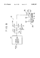
- FIG. 1 is a circuit diagram showing a first embodiment of the present invention
- FIG. 2 is a block diagram showing an application of the first embodiment
- FIGS. 3A and 3B are waveform charts related to the first embodiment
- FIG. 4 shows cross-section potentials in a floating diffusion
- FIG. 5 is a circuit diagram showing a modification of the first embodiment
- FIG. 6 is a circuit diagram showing another modification of the first embodiment
- FIG. 7 is a circuit diagram showing a second embodiment of the present invention.
- FIG. 8 is a block diagram showing an application 1 of the second embodiment
- FIGS. 9A and 9B are waveform charts related to the application 1 in FIG. 8;
- FIG. 10 is a block diagram showing an application 2 of the second embodiment
- FIG. 11 is a waveform chart related to the application 2 in FIG. 10;
- FIG. 12 is a circuit diagram showing an application 3 of the second embodiment
- FIG. 13 is a circuit diagram showing an application 4 of the second embodiment
- FIG. 14 is a circuit diagram showing amodification 1 of the second embodiment
- FIG. 15 is a circuit diagram showing a modification 2 of the second embodiment
- FIG. 16 is a circuit diagram showing a modification 3 of the second embodiment
- FIG. 17 is a block diagram showing a structure of a CCD linear sensor
- FIG. 18 is a block diagram showing a peripheral 11 structure of a charge-voltage converter
- FIG. 19 is a waveform chart of a CCD output obtained without any sample holding action
- FIG. 20 is a waveform chart of a CCD output obtained with a sample holding action
- FIG. 21 is a circuit diagram of a conventional circuit example 1 in the related art.
- FIG. 22 is a circuit diagram of a conventional circuit example 2 in the related art.
- FIGS. 23A and 23B are waveform charts related to the conventional examples.
- FIG. 24 shows cross-section potentials in the vicinity of a floating diffusion.
- FIG. 1 is a circuit diagram showing a first embodiment of the present invention.
- a P-MOS transistor Q11 and an N-MOS transistor Q12 are so arranged that respective gates and drains are mutually connected, and a source of the P-MOS transistor Q11 is connected to a power supply V dd while a source of the N-MOS transistor Q12 is grounded to thereby constitute a first-stage C-MOS inverter 11.
- the gate node N11 of the P-MOS transistor Q11 and the N-MOS transistor Q12 is connected via a signal line L11 to an output terminal of a timing generator circuit 20.
- a P-MOS transistor Q13 and an N-MOS transistor Q14 are so arranged that respective gates and drains are mutually connected, and a source of the P-MOS transistor Q13 is connected to the power supply V dd while a source of the N-MOS transistor Q14 is grounded via a resistor R to thereby constitute a second-stage C-MOS inverter 12.
- the gate node N13 of the P-MOS transistor Q13 and the N-MOS transistor Q14 is connected via a signal line L12 to the drain node N12 of the P-MOS transistor Q11 and the N-MOS transistor Q12.
- the drain node N14 of the P-MOS transistor Q13 and the N-MOS transistor Q14 is connected via a signal line L13 to the output terminal 13.
- a load capacitor CL is connected between the signal line L13 and the ground.
- FIG. 2 is a block diagram showing an application of a switching circuit which is represented by the first embodiment of the above structure.
- the switching circuit of the first embodiment is used as a .o slashed.rs driver 10 for driving a reset gate of a charge-voltage converter which is constructed as, e.g., a floating diffusion amplifier in a charge transfer device 100 such as a charge transfer register or a CCD delay device in a solid-state image sensing apparatus inclusive of a CCD linear sensor or a CCD area sensor.
- the charge-voltage converter for converting a signal charge into a proportional voltage is not limited merely to a floating diffusion amplifier construction alone, and it may be a floating gate construction as well.
- the charge-voltage converter 30 has a switching transistor (MOS transistor) structure which comprises a floating diffusion 32 of N+ type impurity formed adjacent to an output gate 31 of N- type impurity constituting the final stage of a charge transferrer, a reset drain 33 of N+ type impurity formed via a channel region of N type impurity, and a reset gate 34 disposed above the channel region, wherein the signal charge transferred from the output gate 31 to the floating diffusion 32 is converted into a voltage V fd and then is delivered as an output.
- the capacitance (stray capacitance) of the floating diffusion 32 corresponds to the load capacitor CL shown in FIG. 1.
- a predetermined voltage (e.g., supply voltage V dd ) is applied as a reset drain voltage V rd to the reset drain 33.
- a reset pulse .o slashed.rs is applied from the .o slashed.rs driver 10 to the reset gate 34.
- a resistor R is connected between the ground and the source of the N-MOS transistor Q14 in the second-stage C-MOS inverter 12, so that the fall time of the reset pulse .o slashed.rs applied to the reset gate 34 is prolonged as indicated by a solid line in FIG. 3A, whereby the trailing edge of the reset pulse .o slashed.rs can be rendered more obtuse. Accordingly, the high-frequency component can be eliminated in the fall of the reset pulse .o slashed.rs and, as obvious from FIG.
- FIG. 4 shows cross-section potentials of the floating diffusion.
- the one denoted by a single-dot chained line is an on/off threshold level of the reset gate 34.
- a slightly higher potential corresponds to the threshold level.
- V rd a potential equal to the reset drain voltage
- the reset gate voltage obtained when the potential becomes equal to the level V rd is the threshold level V th , and this corresponds to a dotted line traversing the waveform of the reset pulse .o slashed.rs shown in FIG. 3A. Therefore, in the waveform of the reset pulse .o slashed.rs, the slope at the intersection with the threshold level V th is the important fall speed portion concerned with the noise.
- FIG. 5 is a circuit diagram showing a modification of the first embodiment, wherein circuit components corresponding to those in FIG. 1 are denoted by like reference numerals or symbols.
- a resistor R is connected between a signal line L13 and a drain of an N-MOS transistor Q14 in a second-stage C-MOS inverter 12.
- the fall time of the reset pulse .o slashed.rs can be prolonged similarly to the aforementioned case of the first embodiment, so that it becomes possible to reduce the coupling to the output V fd of a floating diffusion 32.
- FIG. 6 is a circuit diagram showing another modification of the first embodiment, wherein circuit components corresponding to those in FIG. 1 are denoted by like reference numerals or symbols.
- a resistor R is connected between a load capacitor CL and a node N14 of a drain of a second-stage C-MOS inverter 12.
- the rise time of the reset pulse .o slashed.rs is also prolonged as well as the fall time thereof, but since the coupling is induced at the fall time of the reset pulse .o slashed.rs, the coupling to the output V fd of a floating diffusion 32 can be reduced without impediment even if the rise time is rendered longer.
- the first embodiment and the modification thereof mentioned above are so constituted as to shape the trailing edge more obtuse in the fall of the reset pulse .o slashed.rs by additionally connecting a resistor R. And it is also possible to achieve further reduction of the .o slashed.rs coupling by a combination with another technique that diminishes the amplitude of the reset pulse .o slashed.rs itself by setting the source potential of the N-MOS transistor Q14 in the second-stage C-MOS inverter 12 not to the ground level but to a potential level V cc which is higher than the ground level but is lower than the voltage level of the power supply V dd .
- FIG. 7 is a circuit diagram showing a second embodiment of the present invention, wherein circuit components corresponding to those in FIG. 1 are denoted by like reference numerals or symbols.
- a P-MOS transistor Q11 and an N-MOS transistor Q12 are so arranged that respective gates and drains are mutually connected, and a source of the P-MOS transistor Q11 is connected to a power supply V dd while a source of the N-MOS transistor Q12 is grounded to thereby constitute a first-stage C-MOS inverter 11.
- the gate node N11 of the P-MOS transistor Q11 and the N-MOS transistor Q12 is connected via a signal line L11 to an output terminal of a timing generator circuit 20.
- a P-MOS transistor Q13 and an N-MOS transistor Q14 are so arranged that respective gates and drains are mutually connected, and a source of the P-MOS transistor Q13 is connected to the power supply V dd while a source of the N-MOS transistor Q14 is grounded via an N-MOS transistor Q15 to thereby constitute a second-stage C-MOS inverter 12.
- a gate of the N-MOS transistor 15 is connected to a node N15 of resistors R1 and R2 connected in series between the power supply V dd and the ground. More specifically, a predetermined voltage obtained by dividing the voltage of the power supply V dd by the resistance ratio of the resistors R1 and R2 is applied to the gate of the N-MOS transistor Q15.
- the N-MOS transistor Q15 and the resistors R1 ad R2 are produced on the same substrate where the other circuit component elements are also mounted (on-chip).
- the gate node N13 of the P-MOS transistor Q13 and the N-MOS transistor Q14 is connected via a signal line L12 to the drain node N12 of the P-MOS transistor Q11 and the N-MOS transistor Q12.
- the drain node N14 of the P-MOS transistor Q13 and the N-MOS transistor Q14 is connected via a signal line L13 to the output terminal 13.
- a load capacitor CL is connected between the signal line L13 and the ground.
- the switching circuit of the second embodiment having the above structure is used as a .o slashed.rs driver 10 for driving a reset gate of a charge-voltage converter which is constructed as, e.g., a floating diffusion amplifier in a charge transfer device 100 such as a charge transfer register or a CCD delay device in a solid-state image sensing apparatus inclusive of a CCD linear sensor or a CCD area sensor, as in the aforementioned case of the first embodiment.
- FIG. 8 is a block diagram showing the structure of its exemplary application.
- a charge-voltage converter 30 is exactly the the same in construction as that in the example of FIG. 2.
- the charge-voltage converter 30 is not limited merely to a floating diffusion amplifier construction alone, and it may be a floating gate construction as well.
- the N-MOS transistor Q15 is connected between the ground and the source of the N-MOS transistor Q14 in the second-stage C-MOS inverter 12, and a predetermined voltage is applied to the gate of the N-MOS transistor Q15, so that this transistor Q15 functions as a constant current source, whereby the fall time alone of the reset pulse .o slashed.rs can be controlled as indicated by a solid line in FIG. 9A, and such control can be so performed as to attain linear fall.
- the signal level (operating point) can be judged with facility due to reduction of the coupling portion of the reset pulse .o slashed.rs in the CCD output waveform, thereby simplifying design of the output circuit connected posterior to the floating diffusion 32. Further, it is rendered possible to set a desired fall speed in the fall of the reset pulse .o slashed.rs by adjusting the gate voltage of the N-MOS transistor Q15 or adjusting the channel length or width of the N-MOS transistor Q15.
- FIG. 10 is a block diagram showing an exemplary application of the second embodiment employed for resetting a diode sensor used as an auto-focus monitor sensor (exposure sensor), wherein circuit components corresponding to those in FIG. 8 are denoted by like reference numerals or symbols.
- FIG. 10 is a block diagram showing an exemplary application of the second embodiment employed for resetting a diode sensor used as an auto-focus monitor sensor (exposure sensor), wherein circuit components corresponding to those in FIG. 8 are denoted by like reference numerals or symbols.
- a diode sensor 40 has a kind of switching transistor (MOS transistor) structure which comprises an N+ type impurity region 42 formed on the obverse side of a P- type impurity region 41, an N+ type impurity region 44 formed beside the N+ type impurity region 42 via an N type impurity region 43, and a reset gate 45 disposed above the N type impurity region 43, wherein the N+ type impurity region 44 is connected to a power supply V dd , and a reset pulse .o slashed.SRS is applied to the reset gate 45.
- MOS transistor switching transistor
- the fall time of a reset pulse .o slashed.SRS can be prolonged while the fall thereof is linearized as graphically shown in FIG. 11. Therefore it becomes possible to reduce the coupling portion of the waveform caused by the capacitive coupling which is derived from the parasitic capacitance between the N+ type impurity region 44 and the reset gate 45 during the fall time (turn-off time) of the reset pulse .o slashed.SRS.
- the fall slope of the reset pulse .o slashed.SRS can be maintained constant, so that the coupling and the noise are not changed by such variation in the threshold level V th .
- FIG. 12 is a block diagram showing an exemplary application of the second embodiment employed for driving a sample hold circuit to perform its sampling action, wherein circuit components corresponding to those in FIG. 8 are denoted by like reference numerals or symbols.
- a sample hold circuit 60 comprises a front-stage buffer 61 consisting of two-stage source followers, a rear-stage buffer 62 consisting of one-stage source follower, a hold transistor (N-MOS transistor) 63 serving as a switching transistor whose drain is connected to an output terminal of the buffer 61 and whose source is connected to an input terminal of the buffer 62, and a hold capacitor 64 connected between the source of the hold transistor 63 and the ground, wherein a sample hold pulse .o slashed.SH is applied to the gate of the hold transistor 63 so that the peak value of an input signal V in is held.
- N-MOS transistor N-MOS transistor
- the switching circuit of the second embodiment By applying the switching circuit of the second embodiment to a .o slashed.SH driver 70 in this manner for driving the sample hold circuit 60 to perform its sampling action, the fall time of a sample hold pulse .o slashed.SH can be prolonged while the fall thereof is linearized. Therefore it becomes possible to reduce the coupling portion of the waveform caused during the fall time of the sample hold pulse .o slashed.SH, hence retaining the output waveform satisfactory with reduction of the S/H coupling. Consequently, due to the use of this sample hold circuit 60 in, e.g., the output circuit of the CCD linear sensor 170 shown in FIG. 17, it is rendered possible to eliminate the necessity of exactly adjusting the timing of the AD converter 182 (FIG. 17) in the rear-stage signal processing, thereby facilitating the design of the circuit.
- FIG. 13 is a block diagram showing an exemplary application of the second embodiment employed for driving a clamp circuit, wherein circuit components corresponding to those in FIG. 8 are denoted by like reference numerals or symbols.
- a clamp circuit 80 comprises a front-stage buffer 81 consisting of two-stage source followers, a rear-stage buffer 82 consisting of one-stage source follower, a clamp capacitor 83 whose one end of connected to an output terminal of the buffer 81 and whose other end is connected to an input terminal of the buffer 82, and a clamp transistor (N-MOS transistor) 85 serving as a switching transistor whose drain is connected to a terminal 84 supplied with a reference potential V ref and whose source is connected to the other end of the clamp capacitor 83, wherein a clamp pulse .o slashed.CLP is applied to the gate of the clamp transistor 85 so that the DC component of the input signal V in is clamped to the reference potential V ref .
- N-MOS transistor N-MOS transistor
- the switching circuit of the second embodiment to a .o slashed.CLP driver 90 for driving the clamp circuit 80, the fall time of a clamp pulse .o slashed.CLP can be prolonged while the fall thereof is linearized. Therefore it becomes possible to reduce the coupling portion of the waveform caused during the fall of the clamp pulse .o slashed.CLP. As a result, the deviation of the clamped DC component from the reference potential V ref is to consequently facilitate design of the rear-stage signal processing circuit.
- the N-MOS transistor Q15 is additionally connected between the ground and the source of the N-MOS transistor Q14 in the second-stage C-MOS inverter 12, and a predetermined potential is applied to the gate of the N-MOS transistor Q15 to thereby shape the trailing edge more obtuse in the fall of the reset pulse .o slashed.rs.
- the resistors R1 and R2, through which the gate voltage is applied to the N-MOS transistor Q15 connected additionally, are so provided as to form an on-chip structure.
- the fall time of the reset pulse .o slashed.rs can be externally controlled by a modification where, as shown in FIG. 14, a gate terminal 14 is provided for the N-MOS transistor Q15, and a gate voltage V g is supplied to the N-MOS transistor Q15 via the gate terminal 14 thereof. It is also possible to externally control the fall time of the reset pulse .o slashed.rs in a configuration where the resistors R1 and R2 are variable ones disposed outside.
- FIG. 15 is a circuit diagram showing another modification of the second embodiment, wherein circuit components corresponding to those in FIG. 7 are denoted by like reference numerals or symbols.
- a depletion type MOS transistor is used as an N-MOS transistor Q15' connected between the ground and the source of an N-MOS transistor Q14 in a second-stage C-MOS inverter 12.
- the depletion type MOS transistor is such that a drain current flows therein without supply of any voltage to its gate.
- the gate of the N-MOS transistor Q15' has the ground level, it is not necessary to provide any exclusive means for generating a gate voltage, and despite occurrence of any variation in the voltage of the power supply V dd , the fall time of the reset pulse .o slashed.rs is not affected by such variation.
- FIG. 16 is a circuit diagram showing a further modification of the second embodiment, wherein circuit components corresponding to those in FIG. 7 are denoted by like reference numerals or symbols.
- a P-MOS transistor Q16 is connected between a power supply V dd and the source of a P-MOS transistor Q13 in a second-stage C-MOS inverter 12, and a divided voltage obtained through resistors R1 and R2 is applied to the gate thereof.
- resistors R1 and R2 is applied to the gate thereof.
- the present invention is so contrived as to shape the trailing edge more obtuse in the fall of the driving pulse applied to the gate of the switching transistor, thereby reducing the coupling portion of the output waveform derived from capacitive coupling.
Landscapes
- Solid State Image Pick-Up Elements (AREA)
- Transforming Light Signals Into Electric Signals (AREA)
- Analogue/Digital Conversion (AREA)
Applications Claiming Priority (2)
| Application Number | Priority Date | Filing Date | Title |
|---|---|---|---|
| JP7-060341 | 1995-03-20 | ||
| JP06034195A JP3309630B2 (ja) | 1995-03-20 | 1995-03-20 | スイッチング回路およびこれを用いた電荷転送装置 |
Publications (1)
| Publication Number | Publication Date |
|---|---|
| US5907357A true US5907357A (en) | 1999-05-25 |
Family
ID=13139375
Family Applications (1)
| Application Number | Title | Priority Date | Filing Date |
|---|---|---|---|
| US08/617,565 Expired - Lifetime US5907357A (en) | 1995-03-20 | 1996-03-19 | Switching circuit and charge transfer device using same |
Country Status (5)
| Country | Link |
|---|---|
| US (1) | US5907357A (de) |
| EP (1) | EP0734026B1 (de) |
| JP (1) | JP3309630B2 (de) |
| CA (1) | CA2171604C (de) |
| DE (1) | DE69624524T2 (de) |
Cited By (14)
| Publication number | Priority date | Publication date | Assignee | Title |
|---|---|---|---|---|
| WO2000078034A3 (en) * | 1999-06-15 | 2001-05-10 | Photobit Corp | Dual sensitivity image sensor |
| US20020032545A1 (en) * | 2000-08-03 | 2002-03-14 | Keiji Mabuchi | Solid-state image pickup device and camera system |
| US20020163584A1 (en) * | 2001-05-02 | 2002-11-07 | Fujitsu Limited | CMOS sensor circuit having a voltage control circuit controlling a gate potential of a photodiode reset transistor to a potential other than power source potentials |
| US6600513B1 (en) * | 1998-01-30 | 2003-07-29 | Sharp Kabushiki Kaisha | Charge transfer device |
| US6674471B1 (en) * | 1998-06-05 | 2004-01-06 | Matsushita Electric Industrial Co., Ltd. | Solid-state imaging device and method for driving the same |
| US20050001915A1 (en) * | 2003-04-18 | 2005-01-06 | Keiji Mabuchi | Solid-state imaging device and drive control method for the same |
| US20050024525A1 (en) * | 2003-07-30 | 2005-02-03 | Takumi Yamaguchi | Solid-state imaging device, camera, power supply device and method thereof |
| US6972794B1 (en) | 1999-06-15 | 2005-12-06 | Micron Technology, Inc. | Dual sensitivity image sensor |
| US7312825B1 (en) * | 1998-05-12 | 2007-12-25 | Sony Corporation | Solid-state image pick device having a timing pulse generator, and method for replacing signals from a switch |
| US20080079685A1 (en) * | 2006-09-29 | 2008-04-03 | Semiconductor Energy Laboratory Co., Ltd. | Display device |
| US20100002112A1 (en) * | 2001-11-06 | 2010-01-07 | Candela Microsystems, Inc. | Cmos image sensor with noise cancellation |
| TWI422220B (zh) * | 2008-09-25 | 2014-01-01 | 新力股份有限公司 | A camera element control method, a camera and an image pickup sensor |
| US8742822B2 (en) | 2012-08-16 | 2014-06-03 | Kabushiki Kaisha Toshiba | Level shift circuit |
| US10547806B2 (en) * | 2016-04-14 | 2020-01-28 | Sony Corporation | Solid-state imaging element, method for operating solid-state imaging element, imaging device, and electronic equipment |
Families Citing this family (3)
| Publication number | Priority date | Publication date | Assignee | Title |
|---|---|---|---|---|
| TWI585730B (zh) * | 2006-09-29 | 2017-06-01 | 半導體能源研究所股份有限公司 | 顯示裝置和電子裝置 |
| JP4674589B2 (ja) * | 2007-02-05 | 2011-04-20 | ソニー株式会社 | 固体撮像装置および撮像装置 |
| US8963904B2 (en) | 2010-03-22 | 2015-02-24 | Apple Inc. | Clock feedthrough and crosstalk reduction method |
Citations (2)
| Publication number | Priority date | Publication date | Assignee | Title |
|---|---|---|---|---|
| US4999676A (en) * | 1989-03-27 | 1991-03-12 | Casio Computer Co., Ltd. | Image forming apparatus having common signal lines |
| US5623221A (en) * | 1992-02-28 | 1997-04-22 | Hitachi, Ltd. | Low noise MOSFET employing selective drive signals |
Family Cites Families (4)
| Publication number | Priority date | Publication date | Assignee | Title |
|---|---|---|---|---|
| EP0031583B1 (de) * | 1979-12-26 | 1988-08-17 | Kabushiki Kaisha Toshiba | Treiberschaltung für eine ladungsgekoppelte Vorrichtung |
| JPS56164681A (en) * | 1980-05-22 | 1981-12-17 | Matsushita Electronics Corp | Solidstate image pick-up device |
| JP2564272B2 (ja) * | 1986-03-14 | 1996-12-18 | 株式会社日立製作所 | 固体撮像装置の信号読み出し装置 |
| JPS635553A (ja) * | 1986-06-25 | 1988-01-11 | Fujitsu Ltd | バツフア回路 |
-
1995
- 1995-03-20 JP JP06034195A patent/JP3309630B2/ja not_active Expired - Lifetime
-
1996
- 1996-03-12 CA CA002171604A patent/CA2171604C/en not_active Expired - Fee Related
- 1996-03-15 DE DE69624524T patent/DE69624524T2/de not_active Expired - Lifetime
- 1996-03-15 EP EP96104156A patent/EP0734026B1/de not_active Expired - Lifetime
- 1996-03-19 US US08/617,565 patent/US5907357A/en not_active Expired - Lifetime
Patent Citations (2)
| Publication number | Priority date | Publication date | Assignee | Title |
|---|---|---|---|---|
| US4999676A (en) * | 1989-03-27 | 1991-03-12 | Casio Computer Co., Ltd. | Image forming apparatus having common signal lines |
| US5623221A (en) * | 1992-02-28 | 1997-04-22 | Hitachi, Ltd. | Low noise MOSFET employing selective drive signals |
Cited By (38)
| Publication number | Priority date | Publication date | Assignee | Title |
|---|---|---|---|---|
| US6600513B1 (en) * | 1998-01-30 | 2003-07-29 | Sharp Kabushiki Kaisha | Charge transfer device |
| US7312825B1 (en) * | 1998-05-12 | 2007-12-25 | Sony Corporation | Solid-state image pick device having a timing pulse generator, and method for replacing signals from a switch |
| US6674471B1 (en) * | 1998-06-05 | 2004-01-06 | Matsushita Electric Industrial Co., Ltd. | Solid-state imaging device and method for driving the same |
| US6972794B1 (en) | 1999-06-15 | 2005-12-06 | Micron Technology, Inc. | Dual sensitivity image sensor |
| US7889258B2 (en) | 1999-06-15 | 2011-02-15 | Aptina Imaging Corporation | Dual sensitivity image sensor |
| US20100002118A1 (en) * | 1999-06-15 | 2010-01-07 | Wang Yibing Michelle | Dual sensitivity image sensor |
| US7605855B2 (en) | 1999-06-15 | 2009-10-20 | Aptina Imaging Corporation | Dual sensitivity image sensor |
| WO2000078034A3 (en) * | 1999-06-15 | 2001-05-10 | Photobit Corp | Dual sensitivity image sensor |
| US20060050163A1 (en) * | 1999-06-15 | 2006-03-09 | Wang Yibing M | Dual sensitivity image sensor |
| US7545425B2 (en) | 2000-08-03 | 2009-06-09 | Sony Corporation | Solid-state image pickup device and camera system |
| US20050174453A1 (en) * | 2000-08-03 | 2005-08-11 | Sony Corporation | Solid-state image pickup device and camera system |
| US6956606B2 (en) * | 2000-08-03 | 2005-10-18 | Sony Corporation | Solid-state image pickup device and camera system |
| US20020032545A1 (en) * | 2000-08-03 | 2002-03-14 | Keiji Mabuchi | Solid-state image pickup device and camera system |
| US20020163584A1 (en) * | 2001-05-02 | 2002-11-07 | Fujitsu Limited | CMOS sensor circuit having a voltage control circuit controlling a gate potential of a photodiode reset transistor to a potential other than power source potentials |
| US7196726B2 (en) * | 2001-05-02 | 2007-03-27 | Fujitsu Limited | CMOS sensor circuit having a voltage control circuit controlling a gate potential of a photodiode reset transistor to a potential other than power source potentials |
| US20100002112A1 (en) * | 2001-11-06 | 2010-01-07 | Candela Microsystems, Inc. | Cmos image sensor with noise cancellation |
| US8431879B2 (en) | 2003-04-18 | 2013-04-30 | Sony Corporation | Solid-state imaging device and drive control method for the same |
| US9521343B2 (en) | 2003-04-18 | 2016-12-13 | Sony Corporation | Solid state imaging device having bias line providing fixing potential |
| US20050001915A1 (en) * | 2003-04-18 | 2005-01-06 | Keiji Mabuchi | Solid-state imaging device and drive control method for the same |
| US7468750B2 (en) * | 2003-04-18 | 2008-12-23 | Sony Corporation | Solid state imaging device having transition time relationship for drive signals |
| US20090072123A1 (en) * | 2003-04-18 | 2009-03-19 | Sony Corporation | Solid-state imaging device and drive control method for the same |
| US9860471B2 (en) | 2003-04-18 | 2018-01-02 | Sony Corporation | Solid-state imaging device |
| US20050024525A1 (en) * | 2003-07-30 | 2005-02-03 | Takumi Yamaguchi | Solid-state imaging device, camera, power supply device and method thereof |
| CN100394776C (zh) * | 2003-07-30 | 2008-06-11 | 松下电器产业株式会社 | 固体摄像器件、摄像机、电源供给装置及其方法 |
| US7349019B2 (en) | 2003-07-30 | 2008-03-25 | Matsushita Electric Industrial Co., Ltd. | Solid-state imaging device, camera, power supply device and method thereof |
| US20080079685A1 (en) * | 2006-09-29 | 2008-04-03 | Semiconductor Energy Laboratory Co., Ltd. | Display device |
| US8743044B2 (en) | 2006-09-29 | 2014-06-03 | Semiconductor Energy Laboratory Co., Ltd. | Display device |
| US8902145B2 (en) | 2006-09-29 | 2014-12-02 | Semiconductor Energy Laboratory Co., Ltd. | Display device |
| US9536903B2 (en) | 2006-09-29 | 2017-01-03 | Semiconductor Energy Laboratory Co., Ltd. | Display device |
| US9842861B2 (en) | 2006-09-29 | 2017-12-12 | Semiconductor Energy Laboratory Co., Ltd. | Display device |
| US8054279B2 (en) | 2006-09-29 | 2011-11-08 | Semiconductor Energy Laboratory Co., Ltd. | Display device |
| US10297618B2 (en) | 2006-09-29 | 2019-05-21 | Semiconductor Energy Laboratory Co., Ltd. | Display device |
| US10930683B2 (en) | 2006-09-29 | 2021-02-23 | Semiconductor Energy Laboratory Co., Ltd. | Display device |
| US11967598B2 (en) | 2006-09-29 | 2024-04-23 | Semiconductor Energy Laboratory Co., Ltd. | Display device |
| US12107092B2 (en) | 2006-09-29 | 2024-10-01 | Semiconductor Energy Laboratory Co., Ltd. | Display device |
| TWI422220B (zh) * | 2008-09-25 | 2014-01-01 | 新力股份有限公司 | A camera element control method, a camera and an image pickup sensor |
| US8742822B2 (en) | 2012-08-16 | 2014-06-03 | Kabushiki Kaisha Toshiba | Level shift circuit |
| US10547806B2 (en) * | 2016-04-14 | 2020-01-28 | Sony Corporation | Solid-state imaging element, method for operating solid-state imaging element, imaging device, and electronic equipment |
Also Published As
| Publication number | Publication date |
|---|---|
| DE69624524D1 (de) | 2002-12-05 |
| JP3309630B2 (ja) | 2002-07-29 |
| DE69624524T2 (de) | 2003-12-11 |
| CA2171604A1 (en) | 1996-09-21 |
| EP0734026A2 (de) | 1996-09-25 |
| CA2171604C (en) | 2006-10-03 |
| EP0734026A3 (de) | 1999-03-17 |
| JPH08264757A (ja) | 1996-10-11 |
| EP0734026B1 (de) | 2002-10-30 |
Similar Documents
| Publication | Publication Date | Title |
|---|---|---|
| US5907357A (en) | Switching circuit and charge transfer device using same | |
| US5233180A (en) | Light sensor having an integration circuit | |
| US8199235B2 (en) | Image sensing device and imaging system | |
| EP0708555B1 (de) | Photoelektrische Wandlungsvorrichtung | |
| US6323479B1 (en) | Sensor pixel with linear and logarithmic response | |
| GB2115636A (en) | A solid-state imaging device | |
| KR19990030209A (ko) | 광전 변환 장치 | |
| US6791613B2 (en) | Signal processing apparatus | |
| KR20210062633A (ko) | 촬상 소자 및 광 검출 소자 | |
| EP0495500B1 (de) | Ladungsübertragungsanordnung mit Ladungssignaldetektor mit verbesserter Empfindlichkeit sowie mit verbesserter Spannungsverstärkung | |
| US20020163584A1 (en) | CMOS sensor circuit having a voltage control circuit controlling a gate potential of a photodiode reset transistor to a potential other than power source potentials | |
| KR100436074B1 (ko) | 안정한 저전압동작이 가능한 증폭형 고체촬상장치용출력회로 | |
| US4155006A (en) | Driver circuit for a solid-state imaging device | |
| US6862041B2 (en) | Circuit for processing charge detecting signal having FETS with commonly connected gates | |
| KR0144900B1 (ko) | 저전원전압 반도체 장치의 입력버퍼 | |
| US20070001101A1 (en) | Programmable rise/fall time control circuit | |
| KR100279864B1 (ko) | 내장신호증폭기를가진고체이미지픽업장치와그의제어방법 | |
| KR100414862B1 (ko) | 스위칭회로및이것을사용한전하전송장치 | |
| US6665011B1 (en) | Circuit and method for rapid reading of an image cell | |
| JPH09163247A (ja) | 昇圧回路、これを搭載した固体撮像装置並びにこれを用いたバーコードリーダ及びカメラ | |
| JPH1032325A (ja) | スイッチング回路およびこれを用いた電荷転送装置 | |
| JP4408547B2 (ja) | 画像読み取り装置 | |
| EP1353500A2 (de) | Bildsensor | |
| JP2534717B2 (ja) | クランプ回路 | |
| JP3409526B2 (ja) | アナログスイッチ回路 |
Legal Events
| Date | Code | Title | Description |
|---|---|---|---|
| AS | Assignment |
Owner name: SONY CORPORATION, JAPAN Free format text: ASSIGNMENT OF ASSIGNORS INTEREST;ASSIGNOR:MAKI, YASUHITO;REEL/FRAME:007925/0459 Effective date: 19960305 |
|
| STCF | Information on status: patent grant |
Free format text: PATENTED CASE |
|
| FPAY | Fee payment |
Year of fee payment: 4 |
|
| FPAY | Fee payment |
Year of fee payment: 8 |
|
| FEPP | Fee payment procedure |
Free format text: PAYER NUMBER DE-ASSIGNED (ORIGINAL EVENT CODE: RMPN); ENTITY STATUS OF PATENT OWNER: LARGE ENTITY Free format text: PAYOR NUMBER ASSIGNED (ORIGINAL EVENT CODE: ASPN); ENTITY STATUS OF PATENT OWNER: LARGE ENTITY |
|
| FPAY | Fee payment |
Year of fee payment: 12 |