US5835168A - Active matrix liquid crystal having capacitance electrodes connected to pixel electrodes - Google Patents
Active matrix liquid crystal having capacitance electrodes connected to pixel electrodes Download PDFInfo
- Publication number
- US5835168A US5835168A US08/044,001 US4400193A US5835168A US 5835168 A US5835168 A US 5835168A US 4400193 A US4400193 A US 4400193A US 5835168 A US5835168 A US 5835168A
- Authority
- US
- United States
- Prior art keywords
- electrode
- scanning
- pixel
- pixel electrode
- side edge
- Prior art date
- Legal status (The legal status is an assumption and is not a legal conclusion. Google has not performed a legal analysis and makes no representation as to the accuracy of the status listed.)
- Expired - Lifetime
Links
Images


Classifications
-
- G—PHYSICS
- G02—OPTICS
- G02F—OPTICAL DEVICES OR ARRANGEMENTS FOR THE CONTROL OF LIGHT BY MODIFICATION OF THE OPTICAL PROPERTIES OF THE MEDIA OF THE ELEMENTS INVOLVED THEREIN; NON-LINEAR OPTICS; FREQUENCY-CHANGING OF LIGHT; OPTICAL LOGIC ELEMENTS; OPTICAL ANALOGUE/DIGITAL CONVERTERS
- G02F1/00—Devices or arrangements for the control of the intensity, colour, phase, polarisation or direction of light arriving from an independent light source, e.g. switching, gating or modulating; Non-linear optics
- G02F1/01—Devices or arrangements for the control of the intensity, colour, phase, polarisation or direction of light arriving from an independent light source, e.g. switching, gating or modulating; Non-linear optics for the control of the intensity, phase, polarisation or colour
- G02F1/13—Devices or arrangements for the control of the intensity, colour, phase, polarisation or direction of light arriving from an independent light source, e.g. switching, gating or modulating; Non-linear optics for the control of the intensity, phase, polarisation or colour based on liquid crystals, e.g. single liquid crystal display cells
- G02F1/133—Constructional arrangements; Operation of liquid crystal cells; Circuit arrangements
- G02F1/136—Liquid crystal cells structurally associated with a semi-conducting layer or substrate, e.g. cells forming part of an integrated circuit
- G02F1/1362—Active matrix addressed cells
- G02F1/136213—Storage capacitors associated with the pixel electrode
Definitions
- the present invention generally relates to a display device and more particularly, to a liquid crystal display panel employing active elements.
- the array substrate as referred to above includes gate electrode 4 for scanning lines X1-XM, a source electrode 6 for signal lines Y1-YN, and further, thin film transistors (referred to as TFTs hereinafter) 2 formed corresponding to respective intersections, with a drain electrode 7 of the respective TFT being connected to a pixel electrode 3.
- TFTs thin film transistors
- a liquid crystal material 13 is inserted between a substrate 1 constituting the TFT and a confronting electrode 14, and independent pixels are formed between the pixel electrode 3 and confronting ground electrode 16 provided on the confronting substrate 14, with the liquid crystal material 13 functioning as a capacitance equivalently.
- an auxiliary capacitance 12 is added in an electrically parallel relationship thereto depending on the need for improving the holding of the signal voltage.
- FIGS. 2(a) and 2(b) showing the conventional TFT-LCD of the previous stage capacitance type, problems taking place in the planar and sectional constructions in the known arrangement will be described hereinafter.
- the display pixel electrode 3C (i, j) does not perfectly cover the scanning electrode 5Xi-1 at the previous stage in the direction of the line width, and thus, an edge portion of the previous stage electrode 5Xi-1 located close to said display pixel electrode 3C (i, j) is exposed.
- the exposure of the scanning electrode 5Xi-1 in terms of plane through the insulative layer results in the local lowering of transmission factor due to the non-uniformity of signal potential within the pixels arising from the leakage of the signal potential of the gate into the pixels.
- the potential distribution in the liquid crystal 13 constituting the pixels 3C (i, j) will be represented as shown in FIG. 3, the and thus, non-uniformity of electric field distribution within the pixels 3C (i, j) becomes larger, thereby forming a distribution within one pixel face in a transmittance characteristic of light.
- an essential object of the present invention is to provide a liquid crystal display panel which is so arranged that display potential thereof is not adversely affected by an electric field from the gate electrode of a thin film transistor (referred to as a TFT hereinafter), thereby improving the display quality of a thin film transistor-liquid crystal display (referred to as a TFT-LCD hereinafter).
- a TFT thin film transistor
- Another object of the present invention is to provide a liquid crystal display panel of the above described type which is simple in construction and stable in functioning at high reliability, and can be readily manufactured on a large scale at low cost.
- the liquid crystal display panel has a pattern configuration in which a pixel electrode 3C (i, j) formed, through an inter-layer insulation, with respect to a gate scanning electrode or scanning line 5Xi-1 at the previous stage, covering part of the wiring edge portion at opposite sides of the scanning line Xi-1 at the previous stage by the display pixel electrode C (i, j).
- the auxiliary capacitance Cadd is formed between the scanning line Xi-1 controlling the display pixel electrode C (i-1, j) at a previous stage of said display pixel electrode C (i, j) and said display pixel electrode C (i, j), and disposed in such a positional relationship that said display pixel electrode C (i, j) covering part of the wiring edge portion at opposite sides of the scanning line Xi-1 at the previous stage by the display pixel electrode C (i, j).
- the gate electrode 5Xi-1 is hidden by the pixel electrode 3C (i, j) as observed in terms of a plane, and the leakage of potentials of the gate electrodes 4 and 5 onto the pixel electrode 3C (i, j) is suppressed. Accordingly, it becomes possible to prevent the non-uniformity of the display potential within the display electrode 3C (i, j) due to the leaking electric field of the gate potential.
- the display portion is to be hidden by 4 ⁇ m which is the combining margin between the black matrix 15 and the pixel 3C, and thus, the display aperture ratio of the pixel can be improved by that extent.
- the display pixel portion formed with black matrix in the conventional arrangement was 72 ⁇ m longitudinally and 72 ⁇ m laterally, with the display pixel aperture ratio of 52%.
- the display pixel portion is 76 ⁇ m longitudinally and 76 ⁇ m laterally, with aperture ratio at 58%, thus showing an improvement of as much as 6% over the conventional construction.
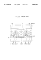
- FIG. 1(a) is a fragmentary top plane view of a TFT-LCD according to one preferred embodiment of the present invention
- FIG. 1(b) is a fragmentary side sectional view on an enlarged scale, of the TFT-LCD of FIG. 1;
- FIG. 2(a) is a fragmentary top plane view of a conventional TFT-LCD having a previous stage capacitance
- FIG. 2(b) is a fragmentary side sectional view on an enlarged scale of the conventional TFT-LCD of FIG. 2(a);
- FIG. 3 is a schematic cross-sectional diagram for explaining the non-uniformity of potential distribution in the pixel within a liquid crystal for the conventional arrangement
- FIG. 4 is a schematic fragmentary cross-section showing a first step for forming the TFT array according to one preferred embodiment of the present invention
- FIG. 5 is a cross-section similar to FIG. 4, which particularly shows a second step therefor;
- FIG. 6 is a cross-section similar to FIG. 4, which particularly shows a third step therefor;
- FIG. 7 is a fragmentary cross-sectional view showing a TFT array according to a second embodiment of the present invention.
- FIG. 8 is also a fragmentary cross-sectional view similar to FIG. 7, which particularly shows a third embodiment of the present invention.
- FIG. 9(a) is a top plane view similar to FIG. 1, which particularly shows a planer positional relationship of a black matrix formed on the TFT-LCD in accordance with an embodiment of the present invention, with respect to the pixel electrode;
- FIG. 9(b) is a schematic fragmentary side sectional view taken along the line IX(b)--IX(b) in FIG. 9(a), showing a side sectional positional relationship of the black matrix formed on the TFT-LCD in accordance with an embodiment of the present invention, with respect to the pixel electrode.
- liquid crystal display device according to the present invention will be described hereinafter.
- FIGS. 1(a) and 1(b) show the construction of an array for a TFT liquid crystal display device according to one preferred embodiment of the present invention.
- the gate electrode 4 of the TFT 2 for driving the display electrode 3C (i, j) is connected to scanning line 4Xi, and the display pixel 3C (i, j) forms an auxiliary capacitance 12 with respect to the scanning line 5Xi-1 at a previous stage through the gate insulative layer 8.
- a substrate including a transparent substrate 1, and gate electrode 4Xi (i 1-M), 5Xi-1, a gate insulative layer 8 formed by P-CVD method, etc., which are formed on said substrate 1, and a semi-conductor layer 9 with a channel protective layer 10 and another semi-conductor layer 9' doped with impurities for ohmic contact further formed on said semi-conductor layer 9 with a channel protective layer 10 is prepared as shown in FIG. 4.
- a transparent layer which serves as the pixel electrode 3C (i, j) is formed, it is so arranged that the gate electrode 5Xi-1 at the previous stage is completely covered thereby, so as to form said pixel electrode 3C (i, j) and its auxiliary electrode 12 Cadd as illustrated in FIG. 5.
- source electrode 6 and drain electrode 7 are formed on the substrate, thereby to forming the TFT array in a matrix pattern.
- SiN ⁇ 18 deposited by a P-CVD method or the like is formed on said substrate with the pixel portion opened thereon.
- the pixel electrode 3C (i, j) is positioned at the upper layer from the source electrode 6 and the drain electrode 7 through the insulative layer 18, with the gate electrode 5Xi-1 at the previous stage covering part of the wiring edge portion at opposite sides of the scanning line Xi-1 at the previous stage by the auxiliary capacitance electrode 21 connected to the display pixel electrode C(i, j). Moreover, the pixel electrode 3C (i, j) is connected with the drain electrode 7 and capacitance electrode 21 through contact holes 19 formed in the insulative layer 18 located at the lower layer of the pixel electrode 3C (i, j).
- a TFT array according to a third embodiment of the present invention as shown in FIG. 8, in the positional relationship in the cross-section, of the pixel electrode 3C (i, j), the source electrode 6, and the drain electrode 7, said pixel electrode 3C (i, j) is located at a lower layer than said source electrode 6, the drain electrode 7, and capacitance electrode 21.
- the pixel electrode 3 and the drain electrode 7 are connected through contact holes 19 formed in the insulative layer 8 provided on said pixel electrode.
- an edge portion of the gate electrode 5Xi-1 at the previous stage near the pixel electrode 3C (i, j) with respect to the direction of line width is covered by the electrode 21 connected to the pixel electrode 3C (i, j) or the gate electrode 5Xi-1 is covering part of the wiring edge portion at opposite sides of the scanning line Xi-1 at the previous stage by the auxiliary capacitance electrode 21 connected to the display pixel electrode C (i, j).
- the black matrix may be formed by utilizing the black matrix 15 provided on the confronting substrate 14 holding the liquid crystal 13 with respect to the TFT array substrate, and part of the gate electrode 5Xi-1 covered by the auxiliary electrode 12, by which arrangement, since the gate portion 20 not covered by the black matrix 15 on the confronting substrate 14 is covered by the pixel electrode 3C (i, j), it is a region not affected by the gate electric field.
- transmission light is shielded by the gate electrode to serve as the black matrix, and further, owing to the fact that the electric field within the pixels is not affected by the gate electric field, the electric field of the transmission pixel portion may be made uniform.
- the non-uniformity of the potential within the pixels and lowering of the aperture ratio which are the problems in the display quality for the TFT-LCD can be remarkably improved by covering the gate electrode with the pixel electrode.
- the black matrix width is held constant, in the case of 100 ⁇ m square pitch pixel, the width of the black matrix at 28 ⁇ m in the conventional arrangement may be reduced to 24 ⁇ m according to the present invention, while in the aperture ratio at 52% can be improved to 58%.
- 19% in the conventional example may be improved to 27% according to the present invention. Therefore, the arrangement of the present invention displays more effect as the pixel density becomes higher.
- the simple construction is adopted to form the auxiliary capacitance with respect to the scanning line, the TFT array may be constituted without increasing the number of masks, and thus, it becomes possible to improve the display quality not requiring particular cost increase.
Landscapes
- Physics & Mathematics (AREA)
- Engineering & Computer Science (AREA)
- Nonlinear Science (AREA)
- Power Engineering (AREA)
- Microelectronics & Electronic Packaging (AREA)
- Mathematical Physics (AREA)
- Chemical & Material Sciences (AREA)
- Crystallography & Structural Chemistry (AREA)
- General Physics & Mathematics (AREA)
- Optics & Photonics (AREA)
- Liquid Crystal (AREA)
- Devices For Indicating Variable Information By Combining Individual Elements (AREA)
Abstract
Description
Claims (7)
Priority Applications (1)
| Application Number | Priority Date | Filing Date | Title |
|---|---|---|---|
| US08/443,663 US5574582A (en) | 1992-04-10 | 1995-05-18 | Active matrix liquid crystal display panel with scanning electrodes acting as capacitor electrode and black matrix |
Applications Claiming Priority (2)
| Application Number | Priority Date | Filing Date | Title |
|---|---|---|---|
| JP4-090506 | 1992-04-10 | ||
| JP9050692A JP2907629B2 (en) | 1992-04-10 | 1992-04-10 | LCD panel |
Related Child Applications (1)
| Application Number | Title | Priority Date | Filing Date |
|---|---|---|---|
| US08/443,663 Division US5574582A (en) | 1992-04-10 | 1995-05-18 | Active matrix liquid crystal display panel with scanning electrodes acting as capacitor electrode and black matrix |
Publications (1)
| Publication Number | Publication Date |
|---|---|
| US5835168A true US5835168A (en) | 1998-11-10 |
Family
ID=14000385
Family Applications (2)
| Application Number | Title | Priority Date | Filing Date |
|---|---|---|---|
| US08/044,001 Expired - Lifetime US5835168A (en) | 1992-04-10 | 1993-04-08 | Active matrix liquid crystal having capacitance electrodes connected to pixel electrodes |
| US08/443,663 Expired - Lifetime US5574582A (en) | 1992-04-10 | 1995-05-18 | Active matrix liquid crystal display panel with scanning electrodes acting as capacitor electrode and black matrix |
Family Applications After (1)
| Application Number | Title | Priority Date | Filing Date |
|---|---|---|---|
| US08/443,663 Expired - Lifetime US5574582A (en) | 1992-04-10 | 1995-05-18 | Active matrix liquid crystal display panel with scanning electrodes acting as capacitor electrode and black matrix |
Country Status (4)
| Country | Link |
|---|---|
| US (2) | US5835168A (en) |
| EP (1) | EP0565125B1 (en) |
| JP (1) | JP2907629B2 (en) |
| DE (1) | DE69313496T2 (en) |
Cited By (9)
| Publication number | Priority date | Publication date | Assignee | Title |
|---|---|---|---|---|
| US5923390A (en) * | 1997-06-26 | 1999-07-13 | Hyundai Electronics Industries Co., Ltd. | Liquid crystal display with high aperture ratio and method for manufacturing the same |
| US6014189A (en) * | 1996-11-15 | 2000-01-11 | International Business Machines Corporation | Transmissive liquid crystal cell with trench capacitor |
| US6057904A (en) * | 1996-10-29 | 2000-05-02 | Lg Electronics, Inc. | Insulating layer arrangements for liquid crystal display and fabricating method thereof |
| US6639281B2 (en) | 2001-04-10 | 2003-10-28 | Sarnoff Corporation | Method and apparatus for providing a high-performance active matrix pixel using organic thin-film transistors |
| US6750473B2 (en) * | 1999-08-31 | 2004-06-15 | E-Ink Corporation | Transistor design for use in the construction of an electronically driven display |
| US6757040B1 (en) * | 1999-05-07 | 2004-06-29 | Lg. Philips Lcd Co., Ltd. | Multi-domain liquid crystal display |
| US6781643B1 (en) * | 1999-05-20 | 2004-08-24 | Nec Lcd Technologies, Ltd. | Active matrix liquid crystal display device |
| US20120299074A1 (en) * | 2011-05-24 | 2012-11-29 | Sharp Kabushiki Kaisha | Semiconductor device |
| US10665610B2 (en) | 2000-12-11 | 2020-05-26 | Semiconductor Energy Laboratory Co., Ltd. | Semiconductor device, and manufacturing method thereof |
Families Citing this family (33)
| Publication number | Priority date | Publication date | Assignee | Title |
|---|---|---|---|---|
| US5610739A (en) * | 1994-05-31 | 1997-03-11 | Matsushita Electric Industrial Co., Ltd. | Liquid crystal display unit with a plurality of subpixels |
| US5563727A (en) * | 1994-06-30 | 1996-10-08 | Honeywell Inc. | High aperture AMLCD with nonparallel alignment of addressing lines to the pixel edges or with distributed analog processing at the pixel level |
| US5657101A (en) * | 1995-12-15 | 1997-08-12 | Industrial Technology Research Institute | LCD having a thin film capacitor with two lower capacitor electrodes and a pixel electrode serving as an upper electrode |
| JP3037886B2 (en) * | 1995-12-18 | 2000-05-08 | インターナショナル・ビジネス・マシーンズ・コーポレイション | Driving method of liquid crystal display device |
| KR100247493B1 (en) * | 1996-10-18 | 2000-03-15 | 구본준, 론 위라하디락사 | Structure of active matrix substrate |
| AU6912798A (en) | 1997-06-10 | 1998-12-30 | Lg. Philips Lcd Co., Ltd. | Liquid crystal display with wide viewing angle and method for making it |
| JP3050191B2 (en) | 1997-11-12 | 2000-06-12 | 日本電気株式会社 | Liquid crystal display |
| US6215541B1 (en) * | 1997-11-20 | 2001-04-10 | Samsung Electronics Co., Ltd. | Liquid crystal displays and manufacturing methods thereof |
| FR2772499A1 (en) * | 1997-12-15 | 1999-06-18 | Thomson Lcd | IMPROVEMENT ON MATRIX SCREENS |
| US6335776B1 (en) * | 1998-05-30 | 2002-01-01 | Lg. Philips Lcd Co., Ltd. | Multi-domain liquid crystal display device having an auxiliary electrode formed on the same layer as the pixel electrode |
| KR20000003318A (en) * | 1998-06-27 | 2000-01-15 | 김영환 | Liquid crystal display unit having improving aperature ratio |
| KR100357213B1 (en) | 1998-07-23 | 2002-10-18 | 엘지.필립스 엘시디 주식회사 | Multi-domain liquid crystal display device |
| WO2000008521A1 (en) * | 1998-08-06 | 2000-02-17 | Konovalov Victor A | Liquid-cristal display and the method of its fabrication |
| US6654090B1 (en) | 1998-09-18 | 2003-11-25 | Lg. Philips Lcd Co., Ltd. | Multi-domain liquid crystal display device and method of manufacturing thereof |
| US6525794B1 (en) | 1998-10-19 | 2003-02-25 | Lg. Philips Lcd Co., Ltd. | Multi-domain liquid crystal display device having a dielectric frame controlling alignment of the liquid crystal molecules |
| KR100313949B1 (en) | 1998-11-11 | 2002-09-17 | 엘지.필립스 엘시디 주식회사 | Multi-domain Liquid Crystal Display Device |
| KR100288772B1 (en) * | 1998-11-12 | 2001-05-02 | 윤종용 | Liquid Crystal Display and Manufacturing Method Thereof |
| US6900869B1 (en) | 1998-11-25 | 2005-05-31 | Lg. Philips Lcd Co., Ltd. | Multi-domain liquid crystal display device with particular dielectric structures |
| US6809787B1 (en) * | 1998-12-11 | 2004-10-26 | Lg.Philips Lcd Co., Ltd. | Multi-domain liquid crystal display device |
| KR100339332B1 (en) | 1999-02-08 | 2002-06-03 | 구본준, 론 위라하디락사 | Multi-domain liquid crystal display device |
| US6791647B1 (en) | 1999-02-24 | 2004-09-14 | Lg Philips Lcd Co., Ltd. | Multi-domain liquid crystal display device |
| KR100357216B1 (en) | 1999-03-09 | 2002-10-18 | 엘지.필립스 엘시디 주식회사 | Multi-domain liquid crystal display device |
| KR100519366B1 (en) * | 1999-04-03 | 2005-10-07 | 엘지.필립스 엘시디 주식회사 | Multi-domain liquid crystal display device |
| JP3766563B2 (en) | 1999-05-17 | 2006-04-12 | 株式会社日立製作所 | Liquid crystal display |
| KR100627107B1 (en) | 1999-07-31 | 2006-09-25 | 엘지.필립스 엘시디 주식회사 | Multi-Domain Liquid Crystal Display Device and Method of Fabricating the same |
| US6639641B1 (en) | 1999-11-25 | 2003-10-28 | Lg.Philips Lcd Co., Ltd. | Multi-domain liquid crystal display device |
| JP3792485B2 (en) * | 2000-06-02 | 2006-07-05 | Nec液晶テクノロジー株式会社 | Active matrix liquid crystal display device |
| KR100595296B1 (en) | 2000-06-27 | 2006-07-03 | 엘지.필립스 엘시디 주식회사 | Muti domain liquid crystal display device and method for fabricating the same |
| KR100595295B1 (en) * | 2000-06-27 | 2006-07-03 | 엘지.필립스 엘시디 주식회사 | Multi domain liquide crystal display device and method for fabricating the same |
| US7072017B1 (en) | 2000-06-29 | 2006-07-04 | Lg. Philips Lcd Co., Ltd. | Multi-domain liquid crystal display device having a common-auxiliary electrode and dielectric structures |
| US7088323B2 (en) * | 2000-12-21 | 2006-08-08 | Lg.Philips Lcd Co., Ltd. | Liquid crystal display device and method for fabricating the same |
| AU2003225622A1 (en) * | 2002-03-01 | 2003-09-16 | American Tool Companies, Inc. | Manual leveling rotating laser with swivel head |
| CN107295982B (en) | 2017-02-28 | 2023-10-24 | 深圳市酷伴科技有限公司 | Automatic launcher for playing ball for pet |
Citations (17)
| Publication number | Priority date | Publication date | Assignee | Title |
|---|---|---|---|---|
| JPS6054478A (en) * | 1983-09-06 | 1985-03-28 | Toshiba Corp | Manufacture of drive circuit substrate for display unit |
| US4519678A (en) * | 1982-01-21 | 1985-05-28 | Tokyo Shibaura Denki Kabushiki Kaisha | Liquid crystal display device |
| US4582395A (en) * | 1980-07-31 | 1986-04-15 | Kabushiki Kaisha Suwa Seikosha | Active matrix assembly for a liquid crystal display device including an insulated-gate-transistor |
| JPS61170724A (en) * | 1985-01-25 | 1986-08-01 | Seiko Instr & Electronics Ltd | Substrate for active matrix display device |
| EP0288011A2 (en) * | 1987-04-20 | 1988-10-26 | Hitachi, Ltd. | Liquid crystal display device and method of driving the same |
| JPH0396922A (en) * | 1989-09-09 | 1991-04-22 | Mitsubishi Electric Corp | Matrix type display device |
| US5017984A (en) * | 1988-02-29 | 1991-05-21 | Seikosha Co., Ltd. | Amorphous silicon thin film transistor array |
| US5060036A (en) * | 1988-12-31 | 1991-10-22 | Samsung Electron Devices Co., Ltd. | Thin film transistor of active matrix liquid crystal display |
| US5162933A (en) * | 1990-05-16 | 1992-11-10 | Nippon Telegraph And Telephone Corporation | Active matrix structure for liquid crystal display elements wherein each of the gate/data lines includes at least a molybdenum-base alloy layer containing 0.5 to 10 wt. % of chromium |
| US5182661A (en) * | 1990-06-25 | 1993-01-26 | Nec Corporation | Thin film field effect transistor array for use in active matrix liquid crystal display |
| US5212574A (en) * | 1989-07-05 | 1993-05-18 | Sharp Kabushiki Kaisha | Active matrix board having double-layer scan lines and capacity lines with discontinuous lower scan lines and lower capacity lines |
| US5276540A (en) * | 1990-11-30 | 1994-01-04 | Sharp Kabushiki Kaisha | Active matrix substrate with conductive film covering transparent conductive film portion connecting additional and non-additional capacitance portions of pixel electrode |
| US5305128A (en) * | 1989-12-22 | 1994-04-19 | North American Philips Corporation | Active matrix electro-optic display device with storage capacitors and projection color apparatus employing same |
| US5335102A (en) * | 1990-05-11 | 1994-08-02 | Sharp Kabushiki Kaisha | Liquid crystal display element and method for treating defective pixels therein |
| US5339181A (en) * | 1991-09-05 | 1994-08-16 | Samsung Electronics Co., Ltd. | Liquid crystal display comprising a storage capacitor including the closed-ended electrode for providing a current bath for circumventing break |
| US5402254A (en) * | 1990-10-17 | 1995-03-28 | Hitachi, Ltd. | Liquid crystal display device with TFTS in which pixel electrodes are formed in the same plane as the gate electrodes with anodized oxide films before the deposition of silicon |
| US5414278A (en) * | 1991-07-04 | 1995-05-09 | Mitsushibi Denki Kabushiki Kaisha | Active matrix liquid crystal display device |
Family Cites Families (12)
| Publication number | Priority date | Publication date | Assignee | Title |
|---|---|---|---|---|
| EP0283290B1 (en) * | 1987-03-18 | 1994-09-21 | Matsushita Electric Industrial Co., Ltd. | Video projector |
| JP2592463B2 (en) * | 1987-09-17 | 1997-03-19 | カシオ計算機株式会社 | Thin film transistor panel |
| JPH0814669B2 (en) * | 1988-04-20 | 1996-02-14 | シャープ株式会社 | Matrix type display device |
| JPH0244316A (en) * | 1988-08-05 | 1990-02-14 | Hitachi Ltd | Liquid crystal display device with auxiliary capacity |
| JPH0816756B2 (en) * | 1988-08-10 | 1996-02-21 | シャープ株式会社 | Transmissive active matrix liquid crystal display device |
| JPH0251128A (en) * | 1988-08-12 | 1990-02-21 | Seikosha Co Ltd | Holding capacitor of silicon thin film transistor array |
| JPH02228632A (en) * | 1989-03-01 | 1990-09-11 | Seiko Instr Inc | Electrooptic device and its production |
| JPH07113730B2 (en) * | 1989-09-08 | 1995-12-06 | 三菱電機株式会社 | Liquid crystal display |
| JP2938521B2 (en) * | 1990-07-10 | 1999-08-23 | 株式会社日立製作所 | Liquid crystal display |
| JP3226223B2 (en) * | 1990-07-12 | 2001-11-05 | 株式会社東芝 | Thin film transistor array device and liquid crystal display device |
| US5414547A (en) * | 1991-11-29 | 1995-05-09 | Seiko Epson Corporation | Liquid crystal display device and manufacturing method therefor |
| US5285302A (en) * | 1992-03-30 | 1994-02-08 | Industrial Technology Research Institute | TFT matrix liquid crystal display with compensation capacitance plus TFT stray capacitance constant irrespective of mask misalignment during patterning |
-
1992
- 1992-04-10 JP JP9050692A patent/JP2907629B2/en not_active Expired - Fee Related
-
1993
- 1993-04-08 US US08/044,001 patent/US5835168A/en not_active Expired - Lifetime
- 1993-04-13 EP EP93105927A patent/EP0565125B1/en not_active Expired - Lifetime
- 1993-04-13 DE DE69313496T patent/DE69313496T2/en not_active Expired - Lifetime
-
1995
- 1995-05-18 US US08/443,663 patent/US5574582A/en not_active Expired - Lifetime
Patent Citations (18)
| Publication number | Priority date | Publication date | Assignee | Title |
|---|---|---|---|---|
| US4582395A (en) * | 1980-07-31 | 1986-04-15 | Kabushiki Kaisha Suwa Seikosha | Active matrix assembly for a liquid crystal display device including an insulated-gate-transistor |
| US4519678A (en) * | 1982-01-21 | 1985-05-28 | Tokyo Shibaura Denki Kabushiki Kaisha | Liquid crystal display device |
| JPS6054478A (en) * | 1983-09-06 | 1985-03-28 | Toshiba Corp | Manufacture of drive circuit substrate for display unit |
| JPS61170724A (en) * | 1985-01-25 | 1986-08-01 | Seiko Instr & Electronics Ltd | Substrate for active matrix display device |
| EP0288011A2 (en) * | 1987-04-20 | 1988-10-26 | Hitachi, Ltd. | Liquid crystal display device and method of driving the same |
| US5017984A (en) * | 1988-02-29 | 1991-05-21 | Seikosha Co., Ltd. | Amorphous silicon thin film transistor array |
| US5060036A (en) * | 1988-12-31 | 1991-10-22 | Samsung Electron Devices Co., Ltd. | Thin film transistor of active matrix liquid crystal display |
| US5212574A (en) * | 1989-07-05 | 1993-05-18 | Sharp Kabushiki Kaisha | Active matrix board having double-layer scan lines and capacity lines with discontinuous lower scan lines and lower capacity lines |
| JPH0396922A (en) * | 1989-09-09 | 1991-04-22 | Mitsubishi Electric Corp | Matrix type display device |
| US5305128A (en) * | 1989-12-22 | 1994-04-19 | North American Philips Corporation | Active matrix electro-optic display device with storage capacitors and projection color apparatus employing same |
| US5335102A (en) * | 1990-05-11 | 1994-08-02 | Sharp Kabushiki Kaisha | Liquid crystal display element and method for treating defective pixels therein |
| US5162933A (en) * | 1990-05-16 | 1992-11-10 | Nippon Telegraph And Telephone Corporation | Active matrix structure for liquid crystal display elements wherein each of the gate/data lines includes at least a molybdenum-base alloy layer containing 0.5 to 10 wt. % of chromium |
| US5182661A (en) * | 1990-06-25 | 1993-01-26 | Nec Corporation | Thin film field effect transistor array for use in active matrix liquid crystal display |
| US5402254A (en) * | 1990-10-17 | 1995-03-28 | Hitachi, Ltd. | Liquid crystal display device with TFTS in which pixel electrodes are formed in the same plane as the gate electrodes with anodized oxide films before the deposition of silicon |
| US5402254B1 (en) * | 1990-10-17 | 1998-09-22 | Hitachi Ltd | Liquid crystal display device with tfts in which pixel electrodes are formed in the same plane as the gate electrodes with anodized oxide films before the deposition of silicon |
| US5276540A (en) * | 1990-11-30 | 1994-01-04 | Sharp Kabushiki Kaisha | Active matrix substrate with conductive film covering transparent conductive film portion connecting additional and non-additional capacitance portions of pixel electrode |
| US5414278A (en) * | 1991-07-04 | 1995-05-09 | Mitsushibi Denki Kabushiki Kaisha | Active matrix liquid crystal display device |
| US5339181A (en) * | 1991-09-05 | 1994-08-16 | Samsung Electronics Co., Ltd. | Liquid crystal display comprising a storage capacitor including the closed-ended electrode for providing a current bath for circumventing break |
Non-Patent Citations (4)
| Title |
|---|
| "12:1: High-Resolution 10.3-in Diagonal Multicolor TFT-LCD", Tsumura et al., SID 91 Digest, pp. 215-218, No Date Provided. |
| "8.5: Rear-Projection TV Using High-Resolution a-Si TFT-LCD", Kobayashi et al., SID 89 Digest, pp. 114-116, No Date Provided. |
| 12:1: High Resolution 10.3 in Diagonal Multicolor TFT LCD , Tsumura et al., SID 91 Digest, pp. 215 218, No Date Provided. * |
| 8.5: Rear Projection TV Using High Resolution a Si TFT LCD , Kobayashi et al., SID 89 Digest, pp. 114 116, No Date Provided. * |
Cited By (9)
| Publication number | Priority date | Publication date | Assignee | Title |
|---|---|---|---|---|
| US6057904A (en) * | 1996-10-29 | 2000-05-02 | Lg Electronics, Inc. | Insulating layer arrangements for liquid crystal display and fabricating method thereof |
| US6014189A (en) * | 1996-11-15 | 2000-01-11 | International Business Machines Corporation | Transmissive liquid crystal cell with trench capacitor |
| US5923390A (en) * | 1997-06-26 | 1999-07-13 | Hyundai Electronics Industries Co., Ltd. | Liquid crystal display with high aperture ratio and method for manufacturing the same |
| US6757040B1 (en) * | 1999-05-07 | 2004-06-29 | Lg. Philips Lcd Co., Ltd. | Multi-domain liquid crystal display |
| US6781643B1 (en) * | 1999-05-20 | 2004-08-24 | Nec Lcd Technologies, Ltd. | Active matrix liquid crystal display device |
| US6750473B2 (en) * | 1999-08-31 | 2004-06-15 | E-Ink Corporation | Transistor design for use in the construction of an electronically driven display |
| US10665610B2 (en) | 2000-12-11 | 2020-05-26 | Semiconductor Energy Laboratory Co., Ltd. | Semiconductor device, and manufacturing method thereof |
| US6639281B2 (en) | 2001-04-10 | 2003-10-28 | Sarnoff Corporation | Method and apparatus for providing a high-performance active matrix pixel using organic thin-film transistors |
| US20120299074A1 (en) * | 2011-05-24 | 2012-11-29 | Sharp Kabushiki Kaisha | Semiconductor device |
Also Published As
| Publication number | Publication date |
|---|---|
| US5574582A (en) | 1996-11-12 |
| EP0565125A1 (en) | 1993-10-13 |
| DE69313496D1 (en) | 1997-10-09 |
| EP0565125B1 (en) | 1997-09-03 |
| DE69313496T2 (en) | 1998-02-19 |
| JP2907629B2 (en) | 1999-06-21 |
| JPH05289104A (en) | 1993-11-05 |
Similar Documents
| Publication | Publication Date | Title |
|---|---|---|
| US5835168A (en) | Active matrix liquid crystal having capacitance electrodes connected to pixel electrodes | |
| KR100713188B1 (en) | Active matrix liquid crystal display apparatus | |
| US5331447A (en) | TFT active matrix liquid crystal display devices with plural TFTs in parallel per pixel | |
| US7023502B2 (en) | Semiconductor device having light-shielded thin film transistor | |
| EP0595363B1 (en) | Transmission type active matrix liquid crystal device | |
| US6259200B1 (en) | Active-matrix display apparatus | |
| JP3604106B2 (en) | Liquid crystal display | |
| US6864937B2 (en) | In-plane switching mode liquid crystal display device with peripheral circuit lines for shielding | |
| US8553182B2 (en) | Liquid crystal display device including a light-blocking member | |
| JPH05127195A (en) | Liquid crystal display device | |
| US5610736A (en) | Active matrix type display device in which elongated electrodes underlie the signal lines to form capacitors with the pixel electrodes and manufacturing method | |
| US20080158118A1 (en) | Electrooptic device and electronic device | |
| US6781645B2 (en) | Active matrix liquid crystal display device | |
| KR20000045309A (en) | Thin film transistor liquid crystal display element | |
| JP2002040480A (en) | Liquid crystal display device | |
| KR100265498B1 (en) | Liquid crystal display capable of providing high-density display without causing non-uniformity in luminance | |
| US5654731A (en) | Shielded pixel structure for liquid crystal displays | |
| US6888600B2 (en) | Display panel for a display device | |
| JP3864036B2 (en) | Liquid crystal display | |
| JP2777545B2 (en) | Active matrix liquid crystal display | |
| JP2870075B2 (en) | Thin film transistor panel and liquid crystal display | |
| JP2828981B2 (en) | Liquid crystal display panel | |
| KR20060051838A (en) | Liquid crystal display device | |
| KR100764290B1 (en) | Apparatus for liquid crystal display | |
| KR20170033935A (en) | Liquid crystal display device having a compensting thin film transistor |
Legal Events
| Date | Code | Title | Description |
|---|---|---|---|
| AS | Assignment |
Owner name: MATSUSHITA ELECTRIC INDUSTRIAL CO., LTD., JAPAN Free format text: ASSIGNMENT OF ASSIGNORS INTEREST.;ASSIGNORS:TAKEDA, MAMORU;KOBAYASHI, IKUNORI;REEL/FRAME:006511/0870 Effective date: 19930405 |
|
| STPP | Information on status: patent application and granting procedure in general |
Free format text: APPLICATION UNDERGOING PREEXAM PROCESSING |
|
| FEPP | Fee payment procedure |
Free format text: PAYOR NUMBER ASSIGNED (ORIGINAL EVENT CODE: ASPN); ENTITY STATUS OF PATENT OWNER: LARGE ENTITY |
|
| FPAY | Fee payment |
Year of fee payment: 4 |
|
| REMI | Maintenance fee reminder mailed | ||
| FPAY | Fee payment |
Year of fee payment: 8 |
|
| SULP | Surcharge for late payment |
Year of fee payment: 7 |
|
| AS | Assignment |
Owner name: TOSHIBA MATSUSHITA DISPLAY TECHNOLOGY CO., LTD., J Free format text: ASSIGNMENT OF ASSIGNORS INTEREST;ASSIGNOR:MATSUSHITA ELECTRIC INDUSTRIAL CO., LTD.;REEL/FRAME:019365/0073 Effective date: 20070320 |
|
| FPAY | Fee payment |
Year of fee payment: 12 |
|
| AS | Assignment |
Owner name: JAPAN DISPLAY CENTRAL INC., JAPAN Free format text: CHANGE OF NAME;ASSIGNOR:TOSHIBA MOBILE DISPLAY CO., LTD.;REEL/FRAME:028339/0316 Effective date: 20120330 Owner name: TOSHIBA MOBILE DISPLAY CO., LTD., JAPAN Free format text: CHANGE OF NAME;ASSIGNOR:TOSHIBA MATSUSHITA DISPLAY TECHNOLOGY CO., LTD.;REEL/FRAME:028339/0273 Effective date: 20090525 |