US5657104A - Liquid crystal display device and manufacturing method thereof - Google Patents
Liquid crystal display device and manufacturing method thereof Download PDFInfo
- Publication number
- US5657104A US5657104A US08/584,508 US58450896A US5657104A US 5657104 A US5657104 A US 5657104A US 58450896 A US58450896 A US 58450896A US 5657104 A US5657104 A US 5657104A
- Authority
- US
- United States
- Prior art keywords
- conductive layer
- external
- conductive
- liquid crystal
- electrodes
- Prior art date
- Legal status (The legal status is an assumption and is not a legal conclusion. Google has not performed a legal analysis and makes no representation as to the accuracy of the status listed.)
- Ceased
Links
Images


Classifications
-
- G—PHYSICS
- G02—OPTICS
- G02F—OPTICAL DEVICES OR ARRANGEMENTS FOR THE CONTROL OF LIGHT BY MODIFICATION OF THE OPTICAL PROPERTIES OF THE MEDIA OF THE ELEMENTS INVOLVED THEREIN; NON-LINEAR OPTICS; FREQUENCY-CHANGING OF LIGHT; OPTICAL LOGIC ELEMENTS; OPTICAL ANALOGUE/DIGITAL CONVERTERS
- G02F1/00—Devices or arrangements for the control of the intensity, colour, phase, polarisation or direction of light arriving from an independent light source, e.g. switching, gating or modulating; Non-linear optics
- G02F1/01—Devices or arrangements for the control of the intensity, colour, phase, polarisation or direction of light arriving from an independent light source, e.g. switching, gating or modulating; Non-linear optics for the control of the intensity, phase, polarisation or colour
- G02F1/13—Devices or arrangements for the control of the intensity, colour, phase, polarisation or direction of light arriving from an independent light source, e.g. switching, gating or modulating; Non-linear optics for the control of the intensity, phase, polarisation or colour based on liquid crystals, e.g. single liquid crystal display cells
- G02F1/133—Constructional arrangements; Operation of liquid crystal cells; Circuit arrangements
- G02F1/1333—Constructional arrangements; Manufacturing methods
- G02F1/1345—Conductors connecting electrodes to cell terminals
- G02F1/13452—Conductors connecting driver circuitry and terminals of panels
-
- G—PHYSICS
- G02—OPTICS
- G02F—OPTICAL DEVICES OR ARRANGEMENTS FOR THE CONTROL OF LIGHT BY MODIFICATION OF THE OPTICAL PROPERTIES OF THE MEDIA OF THE ELEMENTS INVOLVED THEREIN; NON-LINEAR OPTICS; FREQUENCY-CHANGING OF LIGHT; OPTICAL LOGIC ELEMENTS; OPTICAL ANALOGUE/DIGITAL CONVERTERS
- G02F1/00—Devices or arrangements for the control of the intensity, colour, phase, polarisation or direction of light arriving from an independent light source, e.g. switching, gating or modulating; Non-linear optics
- G02F1/01—Devices or arrangements for the control of the intensity, colour, phase, polarisation or direction of light arriving from an independent light source, e.g. switching, gating or modulating; Non-linear optics for the control of the intensity, phase, polarisation or colour
- G02F1/13—Devices or arrangements for the control of the intensity, colour, phase, polarisation or direction of light arriving from an independent light source, e.g. switching, gating or modulating; Non-linear optics for the control of the intensity, phase, polarisation or colour based on liquid crystals, e.g. single liquid crystal display cells
- G02F1/133—Constructional arrangements; Operation of liquid crystal cells; Circuit arrangements
- G02F1/1333—Constructional arrangements; Manufacturing methods
- G02F1/1345—Conductors connecting electrodes to cell terminals
-
- H—ELECTRICITY
- H05—ELECTRIC TECHNIQUES NOT OTHERWISE PROVIDED FOR
- H05K—PRINTED CIRCUITS; CASINGS OR CONSTRUCTIONAL DETAILS OF ELECTRIC APPARATUS; MANUFACTURE OF ASSEMBLAGES OF ELECTRICAL COMPONENTS
- H05K3/00—Apparatus or processes for manufacturing printed circuits
- H05K3/36—Assembling printed circuits with other printed circuits
- H05K3/361—Assembling flexible printed circuits with other printed circuits
-
- G—PHYSICS
- G02—OPTICS
- G02F—OPTICAL DEVICES OR ARRANGEMENTS FOR THE CONTROL OF LIGHT BY MODIFICATION OF THE OPTICAL PROPERTIES OF THE MEDIA OF THE ELEMENTS INVOLVED THEREIN; NON-LINEAR OPTICS; FREQUENCY-CHANGING OF LIGHT; OPTICAL LOGIC ELEMENTS; OPTICAL ANALOGUE/DIGITAL CONVERTERS
- G02F1/00—Devices or arrangements for the control of the intensity, colour, phase, polarisation or direction of light arriving from an independent light source, e.g. switching, gating or modulating; Non-linear optics
- G02F1/01—Devices or arrangements for the control of the intensity, colour, phase, polarisation or direction of light arriving from an independent light source, e.g. switching, gating or modulating; Non-linear optics for the control of the intensity, phase, polarisation or colour
- G02F1/13—Devices or arrangements for the control of the intensity, colour, phase, polarisation or direction of light arriving from an independent light source, e.g. switching, gating or modulating; Non-linear optics for the control of the intensity, phase, polarisation or colour based on liquid crystals, e.g. single liquid crystal display cells
- G02F1/133—Constructional arrangements; Operation of liquid crystal cells; Circuit arrangements
- G02F1/1333—Constructional arrangements; Manufacturing methods
- G02F1/1345—Conductors connecting electrodes to cell terminals
- G02F1/13456—Cell terminals located on one side of the display only
-
- H—ELECTRICITY
- H05—ELECTRIC TECHNIQUES NOT OTHERWISE PROVIDED FOR
- H05K—PRINTED CIRCUITS; CASINGS OR CONSTRUCTIONAL DETAILS OF ELECTRIC APPARATUS; MANUFACTURE OF ASSEMBLAGES OF ELECTRICAL COMPONENTS
- H05K1/00—Printed circuits
- H05K1/02—Details
- H05K1/09—Use of materials for the conductive, e.g. metallic pattern
- H05K1/092—Dispersed materials, e.g. conductive pastes or inks
- H05K1/095—Dispersed materials, e.g. conductive pastes or inks for polymer thick films, i.e. having a permanent organic polymeric binder
-
- H—ELECTRICITY
- H05—ELECTRIC TECHNIQUES NOT OTHERWISE PROVIDED FOR
- H05K—PRINTED CIRCUITS; CASINGS OR CONSTRUCTIONAL DETAILS OF ELECTRIC APPARATUS; MANUFACTURE OF ASSEMBLAGES OF ELECTRICAL COMPONENTS
- H05K2201/00—Indexing scheme relating to printed circuits covered by H05K1/00
- H05K2201/03—Conductive materials
- H05K2201/0332—Structure of the conductor
- H05K2201/0364—Conductor shape
- H05K2201/0367—Metallic bump or raised conductor not used as solder bump
-
- H—ELECTRICITY
- H05—ELECTRIC TECHNIQUES NOT OTHERWISE PROVIDED FOR
- H05K—PRINTED CIRCUITS; CASINGS OR CONSTRUCTIONAL DETAILS OF ELECTRIC APPARATUS; MANUFACTURE OF ASSEMBLAGES OF ELECTRICAL COMPONENTS
- H05K2201/00—Indexing scheme relating to printed circuits covered by H05K1/00
- H05K2201/03—Conductive materials
- H05K2201/0332—Structure of the conductor
- H05K2201/0364—Conductor shape
- H05K2201/0373—Conductors having a fine structure, e.g. providing a plurality of contact points with a structured tool
-
- H—ELECTRICITY
- H05—ELECTRIC TECHNIQUES NOT OTHERWISE PROVIDED FOR
- H05K—PRINTED CIRCUITS; CASINGS OR CONSTRUCTIONAL DETAILS OF ELECTRIC APPARATUS; MANUFACTURE OF ASSEMBLAGES OF ELECTRICAL COMPONENTS
- H05K3/00—Apparatus or processes for manufacturing printed circuits
- H05K3/22—Secondary treatment of printed circuits
- H05K3/24—Reinforcing the conductive pattern
- H05K3/245—Reinforcing conductive patterns made by printing techniques or by other techniques for applying conductive pastes, inks or powders; Reinforcing other conductive patterns by such techniques
-
- H—ELECTRICITY
- H05—ELECTRIC TECHNIQUES NOT OTHERWISE PROVIDED FOR
- H05K—PRINTED CIRCUITS; CASINGS OR CONSTRUCTIONAL DETAILS OF ELECTRIC APPARATUS; MANUFACTURE OF ASSEMBLAGES OF ELECTRICAL COMPONENTS
- H05K3/00—Apparatus or processes for manufacturing printed circuits
- H05K3/30—Assembling printed circuits with electric components, e.g. with resistor
- H05K3/32—Assembling printed circuits with electric components, e.g. with resistor electrically connecting electric components or wires to printed circuits
- H05K3/321—Assembling printed circuits with electric components, e.g. with resistor electrically connecting electric components or wires to printed circuits by conductive adhesives
- H05K3/323—Assembling printed circuits with electric components, e.g. with resistor electrically connecting electric components or wires to printed circuits by conductive adhesives by applying an anisotropic conductive adhesive layer over an array of pads
-
- H—ELECTRICITY
- H05—ELECTRIC TECHNIQUES NOT OTHERWISE PROVIDED FOR
- H05K—PRINTED CIRCUITS; CASINGS OR CONSTRUCTIONAL DETAILS OF ELECTRIC APPARATUS; MANUFACTURE OF ASSEMBLAGES OF ELECTRICAL COMPONENTS
- H05K3/00—Apparatus or processes for manufacturing printed circuits
- H05K3/40—Forming printed elements for providing electric connections to or between printed circuits
- H05K3/4007—Surface contacts, e.g. bumps
Definitions
- the invention relates to a liquid crystal display device and method of manufacturing it, and more particularly, relates to a structure of a connection portion existing between a liquid crystal panel and a flexible substrate.
- liquid crystal display have a flexible substrate (referred to as an FPC hereinafter) to connect the liquid crystal display panel to control and drive circuits located outside of the liquid crystal display device.
- FPC Flexible substrate
- An example of the liquid crystal display device is described in the Utility Model (examined) Publication Hei 5-18789, (Japanese Utility Model (unexamined) Publication Hei 2-87473).
- connection portions have a predetermined pitch (namely the space as between adjacent wirings) adapted to the pitch of the external terminals, and the external terminals of the liquid crystal display device and the connection portions of the FPC are electrically connected to each other.
- the anisotropic conductive film is formed on the surface of the connection portion of the flexible substrate, and conductive particles are arranged at equal interval which are made of a couple of ⁇ m fine metal particles, then so plating the connection portion of the flexible substrate so as to contact to the external terminals.
- These heated components are pressed together so that the anisotropic conductive film is crushed and the external terminals and the connection portions are electrically connected to each other through the conductive particles.
- the FPC is adhered to the liquid crystal panel easily by means of the anisotropic conductive film.
- FIGS. 7, 8, 9, and 10 show an example of conventional technology using the heat seal method.
- FIG. 7 is a perspective view showing a connection area for connecting the FPC to the liquid crystal display panel
- FIG. 8 shows an enlarged cross-sectional view of an edge area of the liquid crystal display device.
- transparent electrodes 3 are formed inside of a top substrate 1
- transparent electrodes 4 are also formed inside of a bottom substrate 2.
- a liquid crystal layer 5 which is shown in FIG. 8 is sealed between top substrate 1 and bottom substrate 2, and a display area D is formed on the top substrate 1 as shown in FIG. 7.
- the bottom substrate extends outward beyond in comparison with the edge area of transparent substrate 1, and this extended portion forms an electrode lead-out area 2a.
- External terminals 3a, 4a are respectively connected to transparent electrodes 3, 4, which are transparent, formed in the shape of stripes and are arranged in parallel on the electrode lead-out area 2a.
- connection portion 10a of FPC 10 is placed on the electrode lead-out area 2a as mentioned above and then heated and crimped. It is secured by the adhesive property of the anisotropic conductive film.
- the external terminals 3a, 4a and the conductive lines 12 are electrically connected each other.
- FIG. 9 depicts a printed circuit board 30 on which a liquid crystal drive circuit is mounted and connected to the liquid crystal display device through FPC 10.
- the back side of the conductive lines 12 are also exposed at a connection portion 10b on a circuit board 30, and the exposed area is also covered by the anisotropic conductive film.
- the connection portion 10b is secured to the printing circuit board 30, and the edge area of the conductive line 12 is conductivity connected to connection pads 31.
- the thickness of the conductive layer on external terminals 3a, 4a is between 200 ⁇ and 600 ⁇ . This is a result of a process which the liquid crystal display device is manufactured, and this is much thinner than the thickness between 10 ⁇ m or 40 ⁇ m which is the thickness of the connection pads 30 formed on a printing circuit board 31. Therefore, in the case of crimping the anisotropic conductive film, the space between the FPC and peripheral portion of the external terminals is narrow, so the space where extra adhesive or/and conductive particles can escape is also narrow. Consequently, the contact area with the conductive particles in the anisotropic conductive film becomes much smaller than the connection portion of the connection pads 31.
- connection portion 10a As a result of this configuration, the resistance of the connection portion tends to increase, and the risk of a break in the circuit also increases. To improve this point, there may be a way to form the anisotropic conductive film of connection portion 10a so as to be thinner than connection portion 10b and so on. However, in this way, it is difficult to maintain the quality of the connection portion, and there is a problem that the cost for manufacturing FPC 10 increase, therefore, the problem can not be solved in the above way.
- FIG. 10 is an exploded view of a single connection of line 12 on external terminal 4a. As shown therein, conductive line 12 is misaligned on external terminal 4a by an amount ⁇ . This results in a smaller area of electrical contact, thus making a poorer contact having a high resistivity.
- It is a further object of this invention is to reduce the cost of liquid crystal display device and products using it, and to improve the durability of these products by improving the reliability of the electrically conductive connection portion and the registration rate of such products.
- a liquid crystal display device is provided with a liquid crystal panel having a liquid crystal layer sealed between two substrates and an external terminal electrically connected to an electrode used for applying an electrical field to the liquid crystal layer.
- a flexible substrate includes a connection portion electrically connected to the external terminal, and a conductive layer having a fixed thickness is provided in a predetermined pattern between the external terminal and the connection portion.
- a conductive layer having a fixed thickness is provided in a predetermined pattern between the external terminal, and the connection portion. Pressure supplied from outside is transmitted intensively to the portion between the external terminals and connection portions, and sufficient pressure is supplied to the portion between external terminal and connection portion.
- a connection area formed by the thickness of conductive layer is attached to the connection portion, a contact area of a conductive adhesive provided between the external terminals and the connection portion is broaden. This results in maintaining a predetermined conductivity.
- the occurrence of conductive deterioration caused by stress or heat from outside is reduced. This is especially true in the case when the external terminals and the connection portion are electrically connected by sufficient pressure, when the flexible substrate is transformed along to the plane of by the conductive layer, and when contact pressure and the contact area is increased.
- the conductive layer should preferably be formed on a surface of the external terminal by arranging a stiffened conductive paste in a predetermined pattern. In this way, it is easier to form the conductive layer.
- the conductive paste should preferably be a conductive ink and the conductive layer should preferably be formed by printing. As such, the conductive layer can be formed in low cost.
- the conductive paste should preferably be formed using a carbon particle and a phenol resin as the main ingredient.
- electrical conductivity is sufficient, and making it possible to provide the conductive layer having certain conductivity without losing the conductive layer's shape. This results since the conductive layer is stiffened by heating concurrently with connection.
- the upper side of the conductive layer should preferably be formed having a toughened or irregularly shaped surface. As such, a conductive contact area is broaden and the adhesion force become stronger.
- an adhesive layer should preferably include conductive particles, which contact with the conductive layer, is formed between the external terminal and the connection portion.
- An anisotropic conductivity can be obtained, and as the conductive particles in the adhesive comes in contact with the conductive layer, large contact area and large compression force are obtained. In accordance with this arrangement, and durability of the contact area for the stress and heat from out side are improved.
- the conductive layer should preferably consist of same material with a conductive connection portion for connecting the electrode of the liquid crystal panel and the external terminal. As such, the effect as mentioned above is obtained without adding other fabrication steps.
- a conductive layer is formed in a predetermined pattern on a surface of an external terminal conductivity connected to an electrode for applying an electric field to a liquid crystal layer contained between two substrates of a liquid crystal panel, and a connection portion of a flexible substrate is electrically connected to the external terminal through the conductive layer.
- the conductive layer is formed in a predetermined pattern on the external terminal at the same time of forming with the same material as a conductive connection portion for connecting the electrode and the external terminals conductivity, it is not necessary to add further fabrication steps.
- the liquid crystal display device equipped with this reliable connection portion between a liquid crystal panel and a flexible substrate can be obtained easily and at a low cost.
- the conductive layer is contacted once to both of the two substrate, then eliminating a part of one of the substrates which contacts to the conductive layer, so that upper surface of the conductive layer which remains on other the substrate is formed roughened or irregular surface.
- upper portion of the conductive layer is separated with the substrate which is removed, therefore, it is possible to form the toughened surface of upper side of the conductive layer which remains. As a result, this arrangement of the adhesion force is improved and the contact area is increased.
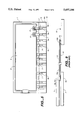
- FIG. 1 a perspective view of a liquid crystal display device in accordance with an embodiment of the present invention
- FIG. 2 is an cross-sectional view showing a connection portion of a liquid crystal panel and a flexible substrate (FPC) of the embodiment of FIG. 1;
- FIG. 2A is an exploded view of the connection area of FIG. 2;
- FIG. 3 is an enlarged cross-sectional view showing the external terminals secured to the FPC of FIG. 1;
- FIG. 4 is an enlarged cross-sectional showing the structure of the FPC
- FIG. 5 is a top view for showing the structure of the liquid crystal display device of the embodiment of the present invention.
- FIGS. 6A-6D are diagrams showing the process of forming the liquid crystal display device in accordance with the present invention.
- FIG. 7 is a top perspective view showing a conventional liquid crystal display device
- FIG. 8 is a cross-sectional view showing a connection portion of a liquid crystal panel and a FPC of the conventional liquid crystal display device
- FIG. 9 is another cross-sectional view of the conventional liquid crystal display device.
- FIGS. 10A and B are exploded perspective views of an external terminal and a conductive line in accordance with the conventional liquid crystal display
- FIGS. 11A and B are exploded perspective views of an external terminal and a conductive line in accordance with the embodiment of FIG. 1;
- FIG. 12 is a plan view of FIG. 10B.
- FIG. 13 is a plan view of FIG. 11B.
- top substrate 1 and bottom substrate 2 made of glass or a transparent resin substrate. Electrodes 3, 4 which are preferably transparent, are formed in a striped shape on an inner surface of the top substrate 1 and an inner surface bottom substrate 2. A liquid crystal layer 5 is then sealed between the top substrate 1 and bottom substrate 2 by seal material 6. A display area D is formed at an outer portion of top substrate 1 corresponding to the liquid crystal layer 5. A refractor (not shown) may be provided on the outer portion of bottom substrate 2. Turning to FIG. 2, bottom substrate 2 extends outwardly beyond substrate 1, forming an exposed electrode lead-out area 2a, on the inner surface of bottom substrate 2. Further, polarization plates (not shown) may be placed on the outer surface of top substrate 1 and the outer surface of bottom substrate 2, in the case of TN (Twisted Nematic) or STN (Super Twisted Nematic) type liquid crystal display devices.
- TN Transmission Nematic
- STN Super Twisted Nematic
- a plurality of external terminals 3a, 4a are aligned and formed on a surface of electrode lead-out area 2a. External terminals 3a, 4a are arranged at predetermined intervals in a stripe shape. The external terminals 3a are electrically connected to transparent electrodes 3 via conductive connector portion 8 which are formed on the inner surface of substrate 1, and external terminals 4a are electrically connected to transparent electrodes 4 which are formed on the inner surface of substrate 2.
- a connection portion 10a of flexible substrate 10 (FPC) is aligned and secured to the position where the external terminals 3a, 4a are formed.
- FPC 10 is provided with a resin sheet 11 which is transparent, and conductive lines 12 made of carbon layer formed on the inner of surface resin sheet 11, (conductive lines 12) are preferably being arranged in parallel.
- FPC 10 further comprises an anisotropic conductive film 13 and a coat layer 14 for covering a portion other than the connection portion 10a.
- Anisotropic conductive film 13 is provided with adhesive materials made of preferably a thermoplastic resin having conductive particles 13b. Conductive particles 13b consist of small carbon particles or metallic particles which are arranged in at predetermined intervals.
- Conductive lines 12 are secured to external terminals 3a, 4a as follows.
- the adhesive material of anisotropic film 13 is melted by applying heat and applying pressure on conductive lines 12 and external terminals 3a, 4a. After anisotropic film 13 has solidified conductive layer 7 is thus secured to conductive line 12, provided secure mechanical and electrical connections.
- FIG. 5 is a top perspective view of the present embodiment.
- External terminals 3a are electrically connected to transparent electrodes 3 (FIG. 2) through conductive connection portion 8 formed by same material of conductive layer 7.
- external terminals 4a are electrically connected to transparent electrodes 4 (FIG. 2) formed on the surface of bottom substrate 2.
- the number and arrangement of external terminals 3a and 4a are defined according to the pattern of transparent electrodes 3, 4 formed on top and bottom sides of liquid crystal layer 5.
- Conductive layer 7 is formed in a predetermined pattern on external lead-out area 2a.
- FIGS. 6A-6D show a process of fabricating the liquid crystal display device in accordance with the present invention.
- external terminals 3a, 4a and transparent electrode 4 are formed in a predetermined pattern on a surface of bottom substrate 2.
- Seal material 60 is secured and arranged surrounding the display area.
- conductive connection pattern 80 to electrically connect top and bottom substrates is formed on external terminals 3a, and a conductive layer pattern 70 is formed on external terminals 3a and 4a by, for example, screen printing using conductive ink.
- conductive ink typically comprises carbon particles dispersed in a phenol resin.
- the shape of conductive layer pattern 70 is a column having a diameter between 0.2 mm and 0.5 mm, which is approximately same as width of the external terminal 3a, 4a and having a thickness of approximately 30 mm.
- transparent electrode 3 having a predetermined pattern is formed on top substrate 1.
- seal material 60, conductive layer pattern 70 and connection pattern 80, for connecting transparent electrodes 3 and to external electrodes 3a are secured on the inner surface of top substrate 1.
- Substrate 1 and substrate 2 are secured by heating at the temperature range of 150° C. to 200° C., and adhering seal material 60, conductive layer pattern 70 and conductive connection pattern 80 between the inner surface of top substrate 1 and the inner surface of bottom substrate 2.
- seal material 60 is completely hardened for forming seal portion 6.
- Top substrate 1 and bottom substrate 2 are secured to each of them by seal portion 6, and conductive layer pattern 70 and conductive connection pattern 80 are secured to the inner surface of top substrate 1 and the inner surface of bottom substrate 2.
- contact portion between substrates 1 and 2 is stiffened periodically.
- the characteristic of stiffness of conductive layer pattern 70 and conductive connection pattern 80 can be regulated by selecting suitable materials or adding additional stiffening agents, such as a polymerization inhibitor to vary the stiffness characteristics of seal material 60.
- top substrate 1 and bottom substrate 2 are cut into individual liquid crystal panels, along lines P1 and P2. Additionally, as shown in FIGS. 6C and 6D, a portion of top substrate 1 is eliminated to form electrode lead-out area 2a along line P4.
- Conductive layer pattern 70 is divided near the middle of the conductive layer 7 when eliminating the part of top substrate 1.
- Conductive layer 7 is formed having a roughened or irregular upper surface 7a. In the preferred embodiment, the thickness of conductive layer 7 is approximately between 10 ⁇ m and 20 ⁇ m. Finally, the device is trimmed along line P3.
- liquid crystal layer 5 is formed by sealing liquid crystal inside of seal portion 6 and securing the FPC 10 shown in FIG. 4 on electrode lead-out area 2a.
- Conductive layer 12 of FPC 10 is arranged on electrode lead-out area 2a in electrical connection with corresponding external terminals 3a, 4a.
- FPC 10 is preferably connected to the liquid crystal panel by heat sealing using a heat crimping tool for applying heat and pressure.
- the conditions of this heat sealing process is, in general, at a temperature range between 130° C. and 150° C. at the surface of pressing side, having a pressure range between 20 kg/cm 3 and 30 kg/cm 3 , and for a time between 5 sec. and 10 sec. It is very important to control the above-discussed conditions, since these conditions can contribute to the reliability of the connection between the liquid crystal panel and FPC 10.
- heat sealing in the range of the condition between 110° C. to 180° C., at the pressure between 15 kg/cm 3 to 50 kg/cm 3 , and at a time between 5 sec. to 10 sec, it would be possible to manufacture the device without causing any problems conductive connection portion.
- a liquid crystal display devices constructed in accordance with the present invention having a pitch for the external terminals 3a, 4a between 0.8 mm and 0.4 mm is reliable and does not exhibit the disadvantages and draw-backs of conventional liquid crystal displays.
- a liquid crystal display device that is heat sealed as mentioned above, adhesive materials 13a of the anisotropic conductive film are melted once, then hardened such that both of conductive line 12 and external terminals 3a, 4a are in contact with conductive particles 13b.
- upper surface of the conductive layer 7 formed on the external terminals 3a, 4a form an electrode lead-out area 2a so that the upper surface of conductive layer 7 and conductive lines 12 are secured as shown in FIG. 3 to provide a reliable electrically conductive connection.
- the contact area with conductive particles in the anisotropic conductive film can be widened, to a space where the anisotropic conductive film can be released and secured by the thickness of the conductive layer 7 as compared to.
- conductive layer 7 is hardened for securing its shape and therefore, conductive layer 7 does not lose its shape.
- external terminals 3a, 4a are made of thin metal film, however, electrode lead-out area 2a are formed having a thickness approximately between 2000 ⁇ to 3000 ⁇ .
- electrode lead-out area 2a are formed having a thickness approximately between 2000 ⁇ to 3000 ⁇ .
- the thickness of conductive layer 7 is in the range of 10 ⁇ m to 20 ⁇ m even the case which the electrode lead-out area 2a is rather thick.
- a length x of conductive line 12 is in contact with external terminal 4a as shown in FIG. 8.
- This length x corresponds to a certain resistivity.
- the length of contact of conductive line 12 is the sum of the contact areas a+b+c+d+e+f+g+h+i which is greater than length x of the conventional device.
- upper surface 7a of the conductive layer 7 is formed having a roughened surface, thus, adhesion force between the upper surface 7a of the conductive layer 7 and the anisotropic film 13 is improved.
- conductive particles 13b are rigidly connected to upper surface 7a, positive electrical connection is achieved. In accordance with this structure, durability and heat resistance of the device are improved.
- the liquid crystal panel and the FPC are adhered by hot adhesion through the anisotropic film 13.
- other techniques such as welding by pasting conductive paste, solder, reflow, or the like or can obtained similar advantages.
- FPC 10 is not limited to an FPC having only wiring, various kinds of the FPC can be employed, such as FPC mounting semiconductor devices and the like.
- conductive layer 7 is formed at the same time and of the same material, it is possible to form the layer without changing the manufacturing process or adding steps. However, needless to say, the conductive layer 7 can be formed in a separate process after forming the electrode lead-out area 2a.
- the conductive layer can not only have a circular shape but can be formed in other shapes such as a rectangle. It is preferable to form the conductive layer in circle or in dotted shape having substantially the same width with the external terminals are aligned along to the direction of the external terminals.
- the invention provides the following effects.
- a conductive layer having a fixed thickness and partially formed between the external terminal and the connection portion external pressure supplied is transmitted intensively to the portion between external terminals and connection portions, and sufficient pressure is supplied to the portion between externals terminal and connection portion, and as the connection formed by the thickness of conductive layer is attached to the portion.
- the contact area of conductive adhesive formed between the external terminals and connection portion are broaden and the good electrical conductivity is kept and maintained. As a result of it, the occurrence of poor conductivity caused by suffering stress or heat from out side is reduced.
- a device constructed in accordance with the present invention provides a secure mechanical and electrical connection even when the flexible substrate is transformed.
- the conductive layer can be formed in low cost by a printing process.
- an anisotropic conductivity can be obtained, and as the conductive particles in the adhesive contacts the conductive layer, a large contact area and a large compression force are obtained, and durability of the contact area for the stress and heat from out side are improved.
- the conductive layer consists of the same material with the conductive connection portion for connecting the electrode of the liquid crystal panel and the external terminal. This results in not increasing the number of manufacturing steps.
- the conductive layer is formed in a predetermined pattern on the external terminal at the same time of forming with and formed by the same material the conductive connection portion it is not necessary to add further steps of process, and the liquid crystal display device can be obtained easily and in low cost.
- the upper surface of the conductive layer prefferably be roughened or irregularly shaped. As a result of this feature, improvement of the adhesion force and an increase of the contact area can be achieved.
- conductive layer 7 is preferably formed in a predetermined pattern, one of ordinary skill in the art would appreciate that it could also be formed in a random pattern.
Landscapes
- Physics & Mathematics (AREA)
- Nonlinear Science (AREA)
- Engineering & Computer Science (AREA)
- Mathematical Physics (AREA)
- Chemical & Material Sciences (AREA)
- Crystallography & Structural Chemistry (AREA)
- General Physics & Mathematics (AREA)
- Optics & Photonics (AREA)
- Manufacturing & Machinery (AREA)
- Microelectronics & Electronic Packaging (AREA)
- Liquid Crystal (AREA)
- Devices For Indicating Variable Information By Combining Individual Elements (AREA)
Priority Applications (1)
| Application Number | Priority Date | Filing Date | Title |
|---|---|---|---|
| US09/801,172 USRE38053E1 (en) | 1995-01-13 | 2001-03-05 | Liquid crystal display device and manufacturing method thereof |
Applications Claiming Priority (4)
| Application Number | Priority Date | Filing Date | Title |
|---|---|---|---|
| JP7-004483 | 1995-01-13 | ||
| JP448295 | 1995-01-13 | ||
| JP7-298276 | 1995-11-16 | ||
| JP29827695A JP3491415B2 (ja) | 1995-01-13 | 1995-11-16 | 液晶表示装置の製造方法 |
Related Child Applications (1)
| Application Number | Title | Priority Date | Filing Date |
|---|---|---|---|
| US09/801,172 Reissue USRE38053E1 (en) | 1995-01-13 | 2001-03-05 | Liquid crystal display device and manufacturing method thereof |
Publications (1)
| Publication Number | Publication Date |
|---|---|
| US5657104A true US5657104A (en) | 1997-08-12 |
Family
ID=26338260
Family Applications (2)
| Application Number | Title | Priority Date | Filing Date |
|---|---|---|---|
| US08/584,508 Ceased US5657104A (en) | 1995-01-13 | 1996-01-11 | Liquid crystal display device and manufacturing method thereof |
| US09/801,172 Expired - Lifetime USRE38053E1 (en) | 1995-01-13 | 2001-03-05 | Liquid crystal display device and manufacturing method thereof |
Family Applications After (1)
| Application Number | Title | Priority Date | Filing Date |
|---|---|---|---|
| US09/801,172 Expired - Lifetime USRE38053E1 (en) | 1995-01-13 | 2001-03-05 | Liquid crystal display device and manufacturing method thereof |
Country Status (3)
| Country | Link |
|---|---|
| US (2) | US5657104A (zh) |
| JP (1) | JP3491415B2 (zh) |
| CN (1) | CN1083109C (zh) |
Cited By (11)
| Publication number | Priority date | Publication date | Assignee | Title |
|---|---|---|---|---|
| US5825450A (en) * | 1996-06-20 | 1998-10-20 | Alps Electric Co., Ltd. | Liquid crystal display device |
| US5864377A (en) * | 1996-11-18 | 1999-01-26 | Samsung Electronics Co., Ltd. | Liquid crystal display |
| US6198519B1 (en) * | 1996-02-28 | 2001-03-06 | Samsung Electronics Co., Ltd. | Liquid crystal display panels including alignment patterns and related methods |
| US6476899B2 (en) * | 2000-09-28 | 2002-11-05 | Minolta Co., Ltd. | Display panel and method of producing the same |
| US20040089884A1 (en) * | 2000-12-29 | 2004-05-13 | Choo Kyo Seop | Thin film transistor array panel and method for fabricating the same |
| US20060036179A1 (en) * | 2001-07-31 | 2006-02-16 | Miller David G | Ultrasound probe wiring method and apparatus |
| US20060152664A1 (en) * | 2004-12-09 | 2006-07-13 | Sanyo Epson Imaging Devices Corp. | Liquid crystal display device |
| US7215404B2 (en) * | 2000-11-25 | 2007-05-08 | Boe-Hydis Technology Co., Ltd. | Liquid crystal display device free from cross talk and fabrication method thereof |
| US20080246744A1 (en) * | 2007-04-09 | 2008-10-09 | Samsung Electronics Co., Ltd | Touch-screen display device |
| US20090322698A1 (en) * | 1999-07-06 | 2009-12-31 | Semiconductor Energy Laboratory Co., Ltd. | Semiconductor device and method of fabricating the same |
| US20100276183A1 (en) * | 2009-04-30 | 2010-11-04 | Nitto Denko Corporation | Flexible printed circuit board |
Families Citing this family (9)
| Publication number | Priority date | Publication date | Assignee | Title |
|---|---|---|---|---|
| TW569062B (en) * | 2001-12-25 | 2004-01-01 | Toshiba Corp | Thermal bonding device and method |
| JP4703955B2 (ja) * | 2003-09-10 | 2011-06-15 | 株式会社 日立ディスプレイズ | 表示装置 |
| KR100740762B1 (ko) * | 2005-02-10 | 2007-07-19 | 오므론 가부시키가이샤 | 접합 방법 및 접합 장치 |
| CN101455132A (zh) * | 2006-05-22 | 2009-06-10 | 皇家飞利浦电子股份有限公司 | 用于相互连接携带大电流的电缆与金属薄膜的互连装置和方法 |
| JP5105487B2 (ja) * | 2009-01-29 | 2012-12-26 | 日本写真印刷株式会社 | 電子機器表示窓のタッチ入力機能付き保護パネル及び電子機器 |
| CN104347154B (zh) * | 2013-07-31 | 2017-11-03 | 南昌欧菲光科技有限公司 | 一种透明导电膜 |
| CN105242433B (zh) * | 2015-10-22 | 2018-05-25 | 深圳市华星光电技术有限公司 | 一种曲面显示模组及电子设备 |
| CN105629527B (zh) * | 2016-01-06 | 2019-01-08 | 京东方科技集团股份有限公司 | 一种探针块、检测装置和显示面板检测方法 |
| KR102451017B1 (ko) | 2017-08-16 | 2022-10-04 | 엘지디스플레이 주식회사 | 플렉서블 표시 장치 |
Citations (10)
| Publication number | Priority date | Publication date | Assignee | Title |
|---|---|---|---|---|
| US4466701A (en) * | 1981-08-25 | 1984-08-21 | Optrex Corporation | Highly reliable electrooptical device and process for manufacturing the same |
| US4631952A (en) * | 1985-08-30 | 1986-12-30 | Chevron Research Company | Resistive hydrocarbon leak detector |
| US4930876A (en) * | 1987-10-30 | 1990-06-05 | Ricoh Company, Ltd. | Liquid crystal display device |
| US5042919A (en) * | 1987-05-01 | 1991-08-27 | Canon Kabushiki Kaisha | External-circuit connecting and packaging structure |
| US5067796A (en) * | 1987-01-26 | 1991-11-26 | Ricoh Company, Ltd. | Liquid crystal display device with cut-out portions in lead electrodes for connection to driving circuit |
| US5100695A (en) * | 1988-11-30 | 1992-03-31 | Nippon Cmk Corp. | Method of manufacturing a printed circuit board |
| US5187604A (en) * | 1989-01-18 | 1993-02-16 | Hitachi, Ltd. | Multi-layer external terminals of liquid crystal displays with thin-film transistors |
| US5317438A (en) * | 1991-08-29 | 1994-05-31 | Ricoh Company, Ltd. | Liquid crystal display device and method of producing the same having an improved connection between a flexible film substrate and a drive circuit substrate |
| US5406164A (en) * | 1993-06-10 | 1995-04-11 | Brother Kogyo Kabushiki Kaisha | Multilayer piezoelectric element |
| US5467210A (en) * | 1993-02-16 | 1995-11-14 | Casio Computer Co., Ltd. | Arrangement of bonding IC chip to liquid crystal display device |
-
1995
- 1995-11-16 JP JP29827695A patent/JP3491415B2/ja not_active Expired - Fee Related
-
1996
- 1996-01-11 US US08/584,508 patent/US5657104A/en not_active Ceased
- 1996-01-12 CN CN96100645A patent/CN1083109C/zh not_active Expired - Fee Related
-
2001
- 2001-03-05 US US09/801,172 patent/USRE38053E1/en not_active Expired - Lifetime
Patent Citations (10)
| Publication number | Priority date | Publication date | Assignee | Title |
|---|---|---|---|---|
| US4466701A (en) * | 1981-08-25 | 1984-08-21 | Optrex Corporation | Highly reliable electrooptical device and process for manufacturing the same |
| US4631952A (en) * | 1985-08-30 | 1986-12-30 | Chevron Research Company | Resistive hydrocarbon leak detector |
| US5067796A (en) * | 1987-01-26 | 1991-11-26 | Ricoh Company, Ltd. | Liquid crystal display device with cut-out portions in lead electrodes for connection to driving circuit |
| US5042919A (en) * | 1987-05-01 | 1991-08-27 | Canon Kabushiki Kaisha | External-circuit connecting and packaging structure |
| US4930876A (en) * | 1987-10-30 | 1990-06-05 | Ricoh Company, Ltd. | Liquid crystal display device |
| US5100695A (en) * | 1988-11-30 | 1992-03-31 | Nippon Cmk Corp. | Method of manufacturing a printed circuit board |
| US5187604A (en) * | 1989-01-18 | 1993-02-16 | Hitachi, Ltd. | Multi-layer external terminals of liquid crystal displays with thin-film transistors |
| US5317438A (en) * | 1991-08-29 | 1994-05-31 | Ricoh Company, Ltd. | Liquid crystal display device and method of producing the same having an improved connection between a flexible film substrate and a drive circuit substrate |
| US5467210A (en) * | 1993-02-16 | 1995-11-14 | Casio Computer Co., Ltd. | Arrangement of bonding IC chip to liquid crystal display device |
| US5406164A (en) * | 1993-06-10 | 1995-04-11 | Brother Kogyo Kabushiki Kaisha | Multilayer piezoelectric element |
Cited By (18)
| Publication number | Priority date | Publication date | Assignee | Title |
|---|---|---|---|---|
| US6198519B1 (en) * | 1996-02-28 | 2001-03-06 | Samsung Electronics Co., Ltd. | Liquid crystal display panels including alignment patterns and related methods |
| US5825450A (en) * | 1996-06-20 | 1998-10-20 | Alps Electric Co., Ltd. | Liquid crystal display device |
| US5864377A (en) * | 1996-11-18 | 1999-01-26 | Samsung Electronics Co., Ltd. | Liquid crystal display |
| US9395584B2 (en) | 1999-07-06 | 2016-07-19 | Semiconductor Energy Laboratory Co., Ltd. | Semiconductor device and method of fabricating the same |
| US9069215B2 (en) | 1999-07-06 | 2015-06-30 | Semiconductor Energy Laboratory Co., Ltd. | Semiconductor device and method of fabricating the same |
| US9052551B2 (en) | 1999-07-06 | 2015-06-09 | Semiconductor Energy Laboratory Co., Ltd. | Semiconductor device and method of fabricating the same |
| US20090322698A1 (en) * | 1999-07-06 | 2009-12-31 | Semiconductor Energy Laboratory Co., Ltd. | Semiconductor device and method of fabricating the same |
| US6476899B2 (en) * | 2000-09-28 | 2002-11-05 | Minolta Co., Ltd. | Display panel and method of producing the same |
| US7215404B2 (en) * | 2000-11-25 | 2007-05-08 | Boe-Hydis Technology Co., Ltd. | Liquid crystal display device free from cross talk and fabrication method thereof |
| US7679084B2 (en) * | 2000-12-29 | 2010-03-16 | Lg Display Co., Ltd. | Thin film transistor array panel and method for fabricating the same |
| US20040089884A1 (en) * | 2000-12-29 | 2004-05-13 | Choo Kyo Seop | Thin film transistor array panel and method for fabricating the same |
| US7715204B2 (en) * | 2001-07-31 | 2010-05-11 | Koninklijke Philips Electronics N.V. | Ultrasound probe wiring apparatus |
| US20060036179A1 (en) * | 2001-07-31 | 2006-02-16 | Miller David G | Ultrasound probe wiring method and apparatus |
| US7432998B2 (en) | 2004-12-09 | 2008-10-07 | Epson Imaging Devices Corporation | Liquid crystal display device |
| US20060152664A1 (en) * | 2004-12-09 | 2006-07-13 | Sanyo Epson Imaging Devices Corp. | Liquid crystal display device |
| US20080246744A1 (en) * | 2007-04-09 | 2008-10-09 | Samsung Electronics Co., Ltd | Touch-screen display device |
| US20100276183A1 (en) * | 2009-04-30 | 2010-11-04 | Nitto Denko Corporation | Flexible printed circuit board |
| US8569629B2 (en) | 2009-04-30 | 2013-10-29 | Nitto Denko Corporation | Flexible printed circuit board |
Also Published As
| Publication number | Publication date |
|---|---|
| JPH08248437A (ja) | 1996-09-27 |
| CN1083109C (zh) | 2002-04-17 |
| JP3491415B2 (ja) | 2004-01-26 |
| CN1152721A (zh) | 1997-06-25 |
| USRE38053E1 (en) | 2003-04-01 |
Similar Documents
| Publication | Publication Date | Title |
|---|---|---|
| US5657104A (en) | Liquid crystal display device and manufacturing method thereof | |
| EP0307231B1 (en) | Display device | |
| US7492434B2 (en) | Display device having an anisotropic-conductive adhesive film | |
| US5155301A (en) | Electrical connection and method for making the same | |
| EP0662256B1 (en) | An electrical connecting structure and a method for electrically connecting terminals to each other | |
| EP1026744A1 (en) | Video display and manufacturing method therefor | |
| JP3763607B2 (ja) | 液晶表示装置の製造方法及び液晶表示装置 | |
| JP2004212587A (ja) | 液晶表示パネル及びこの液晶表示パネルに使用する可撓性基板の実装方法 | |
| JPH0425523B2 (zh) | ||
| JPH0529386A (ja) | 被着体の接続端子部の接続構造 | |
| JP2000347592A (ja) | 平面表示パネルの電極端子接続方法 | |
| JP3810064B2 (ja) | 液晶表示装置 | |
| JP2590094B2 (ja) | 液晶モジュール | |
| JPH04315491A (ja) | プリント配線板 | |
| JPH0419710A (ja) | 液晶表示装置 | |
| JPH10261852A (ja) | ヒートシールコネクタとフレキシブル配線板 | |
| JP3199408B2 (ja) | 液晶パネルの実装方法、液晶パネルの実装構造及び液晶パネルの実装構造の製造方法 | |
| JPH058831B2 (zh) | ||
| KR100389491B1 (ko) | 액정표시장치및그제조방법 | |
| JP3256659B2 (ja) | 異方性導電薄膜および該異方性導電薄膜を使用したポリマー基板接続方法 | |
| JPH0618909A (ja) | 異方性導電膜を有するフレキシブル回路基板 | |
| JP3752836B2 (ja) | 電子部品のボンディング方法 | |
| JP3140163B2 (ja) | 液晶表示装置 | |
| JPH0641266Y2 (ja) | 液晶パネル構造 | |
| JPH0112380Y2 (zh) |
Legal Events
| Date | Code | Title | Description |
|---|---|---|---|
| AS | Assignment |
Owner name: VEDCORP. L.C., VIRGINIA Free format text: SECURITY INTEREST;ASSIGNOR:CYBERMOTION, INC.;REEL/FRAME:007439/0120 Effective date: 19950314 |
|
| AS | Assignment |
Owner name: SEIKO EPSON CORPORATION, JAPAN Free format text: ASSIGNMENT OF ASSIGNORS INTEREST;ASSIGNOR:KANEZAWA, TATSUO;REEL/FRAME:008370/0397 Effective date: 19970118 |
|
| STCF | Information on status: patent grant |
Free format text: PATENTED CASE |
|
| FEPP | Fee payment procedure |
Free format text: PAYOR NUMBER ASSIGNED (ORIGINAL EVENT CODE: ASPN); ENTITY STATUS OF PATENT OWNER: LARGE ENTITY |
|
| FPAY | Fee payment |
Year of fee payment: 4 |
|
| RF | Reissue application filed |
Effective date: 20010306 |