US5652769A - Costas loop and data identification apparatus - Google Patents
Costas loop and data identification apparatus Download PDFInfo
- Publication number
- US5652769A US5652769A US08/551,246 US55124695A US5652769A US 5652769 A US5652769 A US 5652769A US 55124695 A US55124695 A US 55124695A US 5652769 A US5652769 A US 5652769A
- Authority
- US
- United States
- Prior art keywords
- signal
- output
- phase
- oscillation signal
- oscillation
- Prior art date
- Legal status (The legal status is an assumption and is not a legal conclusion. Google has not performed a legal analysis and makes no representation as to the accuracy of the status listed.)
- Expired - Lifetime
Links
- 230000010355 oscillation Effects 0.000 claims abstract description 68
- 230000010354 integration Effects 0.000 claims description 12
- 238000001514 detection method Methods 0.000 claims description 9
- 238000001914 filtration Methods 0.000 claims description 2
- 238000003708 edge detection Methods 0.000 claims 2
- 238000010586 diagram Methods 0.000 description 11
- 238000006243 chemical reaction Methods 0.000 description 5
- 230000003111 delayed effect Effects 0.000 description 4
- 238000005070 sampling Methods 0.000 description 3
- 230000010363 phase shift Effects 0.000 description 2
- 230000001360 synchronised effect Effects 0.000 description 2
- 238000001228 spectrum Methods 0.000 description 1
Images


Classifications
-
- H—ELECTRICITY
- H04—ELECTRIC COMMUNICATION TECHNIQUE
- H04L—TRANSMISSION OF DIGITAL INFORMATION, e.g. TELEGRAPHIC COMMUNICATION
- H04L7/00—Arrangements for synchronising receiver with transmitter
- H04L7/02—Speed or phase control by the received code signals, the signals containing no special synchronisation information
- H04L7/033—Speed or phase control by the received code signals, the signals containing no special synchronisation information using the transitions of the received signal to control the phase of the synchronising-signal-generating means, e.g. using a phase-locked loop
- H04L7/0334—Processing of samples having at least three levels, e.g. soft decisions
-
- H—ELECTRICITY
- H04—ELECTRIC COMMUNICATION TECHNIQUE
- H04L—TRANSMISSION OF DIGITAL INFORMATION, e.g. TELEGRAPHIC COMMUNICATION
- H04L27/00—Modulated-carrier systems
- H04L27/18—Phase-modulated carrier systems, i.e. using phase-shift keying
- H04L27/22—Demodulator circuits; Receiver circuits
- H04L27/227—Demodulator circuits; Receiver circuits using coherent demodulation
- H04L27/2271—Demodulator circuits; Receiver circuits using coherent demodulation wherein the carrier recovery circuit uses only the demodulated signals
- H04L27/2273—Demodulator circuits; Receiver circuits using coherent demodulation wherein the carrier recovery circuit uses only the demodulated signals associated with quadrature demodulation, e.g. Costas loop
-
- H—ELECTRICITY
- H04—ELECTRIC COMMUNICATION TECHNIQUE
- H04L—TRANSMISSION OF DIGITAL INFORMATION, e.g. TELEGRAPHIC COMMUNICATION
- H04L27/00—Modulated-carrier systems
- H04L27/0014—Carrier regulation
- H04L2027/0024—Carrier regulation at the receiver end
- H04L2027/0026—Correction of carrier offset
- H04L2027/0028—Correction of carrier offset at passband only
-
- H—ELECTRICITY
- H04—ELECTRIC COMMUNICATION TECHNIQUE
- H04L—TRANSMISSION OF DIGITAL INFORMATION, e.g. TELEGRAPHIC COMMUNICATION
- H04L27/00—Modulated-carrier systems
- H04L27/0014—Carrier regulation
- H04L2027/0044—Control loops for carrier regulation
- H04L2027/0053—Closed loops
- H04L2027/0057—Closed loops quadrature phase
-
- H—ELECTRICITY
- H04—ELECTRIC COMMUNICATION TECHNIQUE
- H04L—TRANSMISSION OF DIGITAL INFORMATION, e.g. TELEGRAPHIC COMMUNICATION
- H04L27/00—Modulated-carrier systems
- H04L27/0014—Carrier regulation
- H04L2027/0044—Control loops for carrier regulation
- H04L2027/0063—Elements of loops
- H04L2027/0067—Phase error detectors
-
- H—ELECTRICITY
- H04—ELECTRIC COMMUNICATION TECHNIQUE
- H04L—TRANSMISSION OF DIGITAL INFORMATION, e.g. TELEGRAPHIC COMMUNICATION
- H04L27/00—Modulated-carrier systems
- H04L27/0014—Carrier regulation
- H04L2027/0044—Control loops for carrier regulation
- H04L2027/0063—Elements of loops
- H04L2027/0069—Loop filters
Definitions
- the present invention relates to a costas loop and a data identification apparatus. More specifically, the present invention relates to a costas loop which demodulates a BPSK-modulated signal, and a data identification apparatus which identifies whether or not predetermined data is included in a demodulated signal.
- a costas loop after Costas, J. P., or an I-Q loop is disclosed in pages 166-168 of a book "Spread Spectrum System” (R. C. Dixon, translated by Tatsuno Satoshi et al.) JATEC.
- a costas loop 1 a BPSK-modulated signal is multiplied by an oscillation signal from a VCO (Voltage Controlled Oscillator) 3 by a multiplier 2a, and multiplied by the oscillation signal being phase-shifted by a 90° phase-shifter 4 by a multiplier 2b.
- VCO Voltage Controlled Oscillator
- Outputs from the multipliers 2a and 2b are filtered by low-pass filters (LPF) 5a and 5b, respectively, and an output from the LPF 5a is output as a BPSK-demodulated signal, and the outputs from the LPFs 5a and 5b are multiplied with each other by a multiplier 2c. Then, an output of the multiplier 2c is applied to the VCO 3 via a loop filter 6, whereby an oscillation frequency of the VCO 3 is controlled.
- LPF low-pass filters
- the BPSK-modulated signal is represented as " ⁇ A cos ( ⁇ t)"
- the output of the VCO 3 is represented as “cos ( ⁇ t+.increment.)”.
- ".increment.” is an error of phase-shift. Therefore, the output of the multiplier 2a becomes “ ⁇ A(cos.increment.+cos (2 ⁇ t+.increment.))/2", and when the output is filtered by the LPF 5a, a high-frequency component included therein is removed, " ⁇ Acos.increment./2" remains. This component can be approximated to "A/2" when ".increment.” becomes zero, being demodulated data.
- the output of the LPF 5b becomes " ⁇ sin .increment./2" as similar to the above. If the output of the LPF 5a is multiplied by the output of the LPF 5b by the multiplier 2c, a multiplication result becomes "sin (2.increment.)/4". Therefore, when “.increment.” is small, “sin (2.increment.)/4 ⁇ .increment./2” is obtained, and therefore, it is possible to control the VCO 3 such that the ".increment.” becomes zero. In addition, a constant for a control system is set in the loop filter 6.
- costas loop 1 is almost constructed by analog circuits, and therefore, it is difficult to incorporate the costas loop 1 in an integrated circuit. Furthermore, since the costas loop 1 is constructed by analog circuits, there were problems that troublesome adjustment is required and that an influence of a change of temperature is large.
- a principal object of the present invention is to provide a costas loop capable of being easily incorporated in an integrated circuit.
- Another object of the present invention is to provide a data identification circuit suitable for a costas loop constructed by digital circuits.
- a costas loop comprises: a digital signal means which receives a modulated signal and outputs a digital modulated signal; an oscillation signal output means which is controlled by a control signal and outputs a first oscillation signal and a second oscillation signal having a predetermined phase-difference with respect to the first oscillation signal; a first latch means for latching the digital modulated signal according to the first oscillation signal; a second latch means for latching the digital modulated signal according to the second oscillation signal; a phase-comparison means for comparing a phase of the digital modulated signal and a phase of the second oscillation signal with each other on the basis of outputs of the first latch means and the second latch means; and a filter means for filtering a comparison result by the phase-comparison means, wherein an output of the filter means functions as the control signal.
- a second invention is a data identification apparatus which identifies whether or not predetermined data is included in a digital modulated signal, and comprises: a detection means for detecting the number of at least one of "0" and "1" included in the digital demodulated signal of a predetermined length; and a judge means for judging whether or not the predetermined data is included in the digital demodulated signal according to a detection result of the detection means.
- the BPSK-modulated signal such as an RDS (Radio Data System) signal is converted into a binary signal by a comparator, for example, and a digital BPSK-modulated signal is latched by the first latch means such as a D-FF according to an oscillation signal from a VCO, for example, and the digital BPSK-modulated signal is also latched by the second latch means such as a D-FF according to the oscillation signal being phase-shifted by a 90° phase-shifter, for example.
- the output from the first latch means becomes a demodulated signal (RDS signal).
- phase-comparator for example, a phase difference between the BPSK-modulated signal and the oscillation signal from the VCO or a phase difference between the BPSK-modulated signal and the oscillation signal being phase-shifted by 90 degrees is selected according to a calculation result by an EXOR circuit which receives the outputs from the first and second latch means, for example, and the same is outputted as the comparison result.
- a loop filter for example, a divided value obtained by dividing the comparison result by a predetermined value is sequentially integrated by a digital integrator, for example, included in the loop filter, and an integration result and the comparison result from the phase-comparator are added to each other, and an addition result becomes an output of the loop filter.
- a first constant or a second constant is selected, and by a modulo adder, for example, a third constant is subjected to a modulo addition to modulus the first constant or the second constant as selected.
- a carry by the modulo addition is detected by a carry detector, for example, and an output of the carry detector becomes the oscillation signal of the VCO.
- the numbers of "0" and "1" included in the RDS signal which is obtained through the demodulation according to the first invention, for example, and has a predetermined length are counted by a first counter and a second counter, respectively, and it is determined by the judge means whether or not one of count values of the first counter and the second counter is larger than a predetermined value. If one of the count values is larger than the predetermined value, it is determined that an ARI (Autoted Rundfunk Informations) signal, for example, is included in the RDS signal, and a high level signal is outputted from the judge means.
- ARI Automatic Rundfunk Informations
- respective circuits can be made by digital circuits, it is possible to incorporate a costas loop in an integrated circuit.
- the data included in the demodulated signal according to the first invention can be identified.
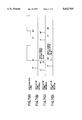
- FIG. 1 is a block diagram showing one embodiment according to a first invention
- FIG. 2 is a block diagram showing a portion of FIG. 1 embodiment
- FIG. 3 is a block diagram showing another portion of FIG. 1 embodiment
- FIG. 4 is a block diagram showing other portion of FIG. 1 embodiment
- FIGS. 5(A)-5(C) are a timing chart showing a portion of an operation of FIG. 1 embodiment
- FIGS. 6(A)-6(C) are a timing chart showing a portion of the operation of FIG. 1 embodiment
- FIG. 7(A) is a waveform chart showing a BPSK-modulated signal
- FIG. 7(B) to 7(D) are waveform charts showing oscillation signals
- FIG. 8(A) is a waveform chart showing the BPSK-modulated signal
- FIG. 8(B) is a waveform chart showing the oscillation signal
- FIG. 8(C) is a waveform chart showing a demodulated signal
- FIG. 9 is a block diagram showing a portion of another embodiment according to the first invention.
- FIG. 10 is a block diagram showing a portion of another embodiment according to the first invention.
- FIG. 11 is a block diagram showing a portion of other embodiment according to the first invention.
- FIG. 12 is a block diagram showing one embodiment according to a second invention.
- FIG. 13(A) is a waveform chart showing the BPSK-modulated signal
- FIG. 13(B) is a waveform chart showing a reproduced clock
- FIG. 13(C) is a waveform chart showing a pulse
- FIG. 14 is a block diagram showing another embodiment according to the second invention.
- FIG. 15 is a block diagram showing a portion of FIG. 12 embodiment.
- FIG. 16 is a block diagram showing a prior art.
- a costas loop 10 of this embodiment shown includes a comparator 12.
- a BPSK-modulated signal of an RDS signal is compared with a reference voltage by the comparator 12, whereby the BPSK-modulated signal is converted into a binary signal.
- the BPSK-modulated signal being a binary signal is applied to D-FFs 14a and 14b, respectively.
- the digital BPSK-modulated signal is latched by the D-FF 14a according to an oscillation signal output from a VCO 16, and the digital BPSK-modulated signal is also latched by the D-FF 14b according to an oscillation signal which is output from the VCO 16 and then phase-shifted by a 90° phase-shifter 18.
- An output signal from the D-FF 14a is output as a demodulated signal (RES signal), and applied to a phase-comparator 20 which also receives an output of the D-FF 14b.
- RES signal demodulated signal
- the oscillation signal output from the VCO 16 the oscillation signal output from the 90° phase-shifter 18 and the digital BPSK-modulated signal are further applied.
- a phase-comparison result is outputted from the phase-comparator 20 on the basis of these signals, and the phase-comparison result is applied to the VCO 16 via a loop filter 22, whereby an oscillation frequency of the VCO 16 is controlled.
- a first oscillation signal is withdrawn from the VCO 16, and a second oscillation signal is withdrawn from the 90° phase-shifter 18.
- a phase-comparator 20 includes a counter 24a which is incremented by a high-speed pulse shown in FIG. 5(C) from an independent clock generator or oscillator and reset by the oscillation signal (FIG. 5(B)) from the 90° phase-shifter 18, and a count value of the counter 24a is applied to a D-FF 26a.
- the D-FF 26a also receives a selection signal from an edge selector 28 which selects only an edge just after the oscillation signal from the 90° phase-shifter 18 is input out of edges of the BPSK-modulated signal shown in FIG. 5(A), whereby the count value is latched.
- the count value as latched indicates the number of the high-speed pulses between the oscillation signal FIG. 5(B) and the edge of the BPSK-modulated signal just after the oscillation signal FIG. 5(A).
- the number of the high-speed pulses between the oscillation signal and the edge of the BPSK-modulated signal is "2" as can be seen from FIG 5(C).
- the edge selector 28 because a frequency of the BPSK-modulated signal is double the oscillation signal, and in the BPSK-modulated signal, there are edges which can not be used for latching the count value, only the edge of the BPSK-modulated signal just after the oscillation signal is input is selected by the edge selector 28.
- the count value latched by the D-FF 26a is added to a constant "0.5" by an adder 29, and an addition result is applied to a selection circuit 30.
- a reason why the constant "0.5" is added to the count value by the adder 29 is that the edges of the BPSK-modulated signal are not in synchronous with the high-speed pulse, and on an average, each edge exists a center between a high-speed pulse and a next high-speed pulse.
- Phase-comparator 20 also includes a counter 24b which is incremented by the high-speed pulse shown in FIG. 6(C) and reset by the BPSK-modulated signal shown in FIG. 6(A), and a count value of the counter 24b is latched by a D-FF 26b according to the oscillation signal (FIG. 6(B)) from the 90° phase-shifter 18. Therefore, the count value as latched indicates the number of the high-speed pulses existing between the edge of the BPSK-modulated signal FIG. 6(A) and the oscillation signal FIG. 6(B) from the 90° phase-shifter 18 just after the edge. In this embodiment shown in FIG. 6, the number of the high-speed pulses existing between the edge of the BPSK-modulated signal and the oscillator signal from the 90° phase-shifter 18 just after the edge is "3" as can be seen from FIG. 6(C).
- a constant "0.5" is subtracted from the count value as latched by a subtracter 32.
- a sign (+or -) of a value from the subtracter 32 is inverted by an inverter 34, and a value having an inverted sign is applied to the selection circuit 30.
- a reason why the constant "0.5" is subtracted by the subtracter 32 is similar to the above described reason.
- a reason why the sign is inverted is that it is necessary to make a phase control reverse with respect to a case of FIG. 5.
- the output signals from the latches 14a and 14b are applied to an EXOR circuit 36, thereby to be subjected to an exclusive logic sum. Therefore, when the phase of the oscillation signal is advanced to the BPSK-modulated signal, as shown in FIG. 7(A) and FIG. 7(C), "0" is output from the EXOR circuit 36. When the phase of the oscillation signal is delayed to the BPSK-modulated signal, as shown in FIG. 7(A) and FIG. 7(D), "1" is output from the EXOR circuit 36. An output of the EXOR circuit 36 is latched by a D-FF 26c according to the oscillation signal from the VCO 16.
- An output of the D-FF 26c is then applied to the selection circuit 30, whereby any one of the signal from the adder 28 and the signal from the inverter 34 is selected. That is, if the output from the D-FF 26c is "0", the signal from the adder 28 is output from the selection circuit 30, and if the output from the D-FF 26c is "1", the signal from the inverter 34 is output from the selection circuit 30.
- a signal thus selected by the selection circuit 30 is output as a phase-comparison result via a D-FF 26d which latches the signal according to the oscillation signal from the VCO 16.
- FIG. 3 Structure of the loop filter 22 to which the phase-comparison result is input is shown in FIG. 3.
- the phase-comparison result is applied to an adder 38a and a divider 40.
- a divider 40 divides the phase-comparison result by "R2", i.e. makes the phase-comparison result "1/R2”, and an output from the divider 40 is applied to an adder 38b which also receives an output of a D-FF 42 which latches an addition result from the adder 38b according to the oscillation signal of the VCO 18, whereby the output of the divider 40 is integrated.
- An output of the D-FF 42 is then added to the phase-comparison result by the adder 38a, and only a sign (+ or -) of an addition result is output from the adder 38a.
- a transfer function of the analog loop filter is represented by the following equation (1).
- the transfer function can be represented by the following equation (2).
- Constants "19019” and "18981” are applied to a selection circuit 44, and one of the constants is selected according to the output from the loop filter 22. That is, if the sign of the output from the loop filter 22 is "+”, the constant "19019” is selected, and if the sign is "-”, the constant "18981” is selected. Furthermore, a constant "250” is applied to an adder 46 in which an output of a D-FF 48 and the constant "250" are added to each other. A selection result by the selection circuit 44 and an addition result of the adder 46 are applied to a calculator 50, and compared with each other by the calculator 50.
- the addition result is output as it is from a terminal A, and a low level signal is output from a terminal B. If the selection result is equal to or smaller than the addition result, "addition result-selection result" is output from the terminal A, and a high level signal is output from the terminal B.
- the D-FF 48 latches an output from the calculator 50 according to the high-speed pulse.
- the frequency of the high-speed pulse is 1824 Hz
- the oscillation frequency becomes 23.976 Hz ( ⁇ 1824 ⁇ 250/19019)
- the constant "18981” is selected by the selection circuit 44
- the oscillation frequency becomes 24.024 Hz ( ⁇ 1824 ⁇ 250/18981). Therefore, if it is required to advance the phase, the constant "18981” may be selected, and if the phase is to be delayed, the constant "19019” may be selected.
- the 90° phase-shifter 18 is constructed by a delay circuit, and by delaying a signal by 1/(24 ⁇ 4) seconds, it is possible to phase-shift by 90 degrees of a signal of 24 Hz.
- the costas loop 10 can be constructed with utilizing digital circuits, it is possible to incorporated the costas loop 10 in an integrated circuit, and accordingly, troublesome adjustment for the circuits become unnecessary, and it is possible to suppress the influence of the change of temperature. Furthermore, since it is not required to provide an LPF as done in a prior art analog costas loop, it is possible to reduce the number of components.
- the dividing value of the divider 40 shown in FIG. 3 is "R2", i.e. "1/R2”; however, if the dividing value is "2 M (M is an integer)", i.e. "1/2 M " as shown in FIG. 9, the output of the divider 40 may be input to the adder 38b with shifting the output by m bits from the MSB.
- a overflow detection circuit 52 which detects that the absolute value of the output of the adder 38b is overflowed, and a gate 54 may be provided as shown in FIG. 10. In such a case, if the overflow is detected by the overflow detection circuit 52, the oscillation signal is inhibitted from being passed through the gate 54.
- phase-comparator 20 may be modified as shown in FIG. 11. More specifically, the phase-comparator 20 shown in FIG. 11 includes a conversion circuit 56 which converts "0" and "1" included in the output of the EXOR circuit 36 and thus the D-FF 26c into “+1" and "-1", respectively. As similar to the above described embodiment, the outputs from the latch circuits 14a and 14b are applied to the EXOR circuit 36, and the VCO 16 may be controlled on the basis of an output of the conversion circuit 56.
- the phase of the oscillation signal is delayed on the basis of "+1" of the output of the conversion circuit 56, and if the output of the D-FF 26c is "-1", by regarding as that the phase of the oscillation signal is delayed, the phase may be advanced on the basis of "-1"of the output of the conversion circuit 56.
- the ARI signal has an amplitude of three times the RDS signal, and the ARI signal and the RDS signal have a quadrative relationship. Therefore, both signals can be represented by the following fomula (4).
- the output of the multiplier 2a is " ⁇ A"
- the output of the multiplier 2a becomes " ⁇ 3A”
- the presence or absence of the ARI signal was determined on the basis of the level.
- a data identification apparatus 60 of one embodiment shown in FIG. 10 can solve such a problem.
- the demodulated signal (FIG. 13(A)) being output from the costas loop 10 shown in FIG. 1 is applied to a clock reproduction circuit 62 by which a clock (FIG. 13(B)) that is in synchronous with the demodulated signal is reproduced.
- a reproduced clock from the reproduction circuit 62 is applied to a pulse generation circuit 64, and a pulse shown in FIG. 13(C) is outputted from the pulse generation circuit 64 at every timing that the clock is applied four times.
- the clock from the clock reproduction circuit 62 and the pulse from the pulse generation circuit 64 are applied to counters 66a and 66b which are incremented by the clock and reset by the pulse. Furthermore, the demodulated signal is applied to the counters 66a and 66b as an enable signal for each of them. Then, if the demodulated signal is "1", the counter 66a is enabled, and when the demodulated signal is "0", the counter 66b is enabled.
- Count values output from the counters 66a and 66b are respectively latched by D-FFs 68a and 68b according to the pulse from the pulse generation circuit 64. Therefore, the count values latched by the D-FFs 68a and 68b indicate the number of "1” and the number of "0", respectively, between adjacent pulses.
- the count values latched by the latches 68a and 68b are applied to the judge circuits 70a and 70b, and it is determined whether or not the number of "1” and the number of "0" are larger than predetermined values, respectively, by the judge circuits 70a and 70b.
- the high level signal is outputted from the judge circuit 70a or 70b, and the same is applied to an OR circuit 72. Therefore, if the number of "1” or the number of "0" is larger than the predetermined value, a high level signal is outputted from the OR circuit 72, and if both of the number of "1” and the number of "0" are respectively smaller than the predetermined values, a low level signal is output from the OR circuit 72.
- the demodulated signal does not contain the ARI signal, the number of "0” and the number of "1” of the demodulated signal are equal to each other; however, if the demodulated signal contains the ARI signal, a portion of the ARI signal in the demodulated signal becomes to have only “0” or "1". Therefore, by counting the number of "1” or "0” included in the demodulated signal, it is possible to identify the ARI data. In addition, actually, since there are data errors, it is determined that the ARI signal is included in the demodulated signal when the number of "1" or "0" is more than the predetermined value.
- a data identification apparatus 60 of another embodiment according to the present invention includes a shift register 74 which fetches the data demodulated signal according to the clock reproduced by the clock reproduction circuit 62, and shifts the data as fetched.
- a logic circuit 76 outputs one of a high level signal and a low level signal according to the number of "0" and the number of "1" in the data within the shift register 74. More specifically, as shown in FIG. 15, when a signal according to the data within the shift register, i.e. the data is "1", the output of the logic circuit 74 becomes a high level, and if the data is "0", the output becomes a low level.
- the output of the logic circuit 76 is applied to an AND circuit 78 and a NAND circuit 80, and output signals from the AND circuit 78 and the NAND circuit 80 are outputted from an OR circuit 82. Therefore, if all the numerals or data within the shift register 74 are "1" or "0", the high level signal is outputted from the logic circuit 76, and if one or more different numerals are included in the shift register 74, the low level signal is outputted from the logic circuit 76.
- the data identification apparatus can be applied to the digital costas loop, and can be incorporated in an integrated circuit.
- the description is made with utilizing the RDS signal and the ARI signal; however, it is needless to say that the present invention can be applied to any kinds of signals capable of being identified by the number of "1" or "0" included in the signal.
Landscapes
- Engineering & Computer Science (AREA)
- Computer Networks & Wireless Communication (AREA)
- Signal Processing (AREA)
- Digital Transmission Methods That Use Modulated Carrier Waves (AREA)
- Stabilization Of Oscillater, Synchronisation, Frequency Synthesizers (AREA)
- Signal Processing For Digital Recording And Reproducing (AREA)
- Mobile Radio Communication Systems (AREA)
Applications Claiming Priority (2)
| Application Number | Priority Date | Filing Date | Title |
|---|---|---|---|
| JP6-266579 | 1994-10-31 | ||
| JP26657994A JP3540393B2 (ja) | 1994-10-31 | 1994-10-31 | コスタスループ |
Publications (1)
| Publication Number | Publication Date |
|---|---|
| US5652769A true US5652769A (en) | 1997-07-29 |
Family
ID=17432775
Family Applications (1)
| Application Number | Title | Priority Date | Filing Date |
|---|---|---|---|
| US08/551,246 Expired - Lifetime US5652769A (en) | 1994-10-31 | 1995-10-31 | Costas loop and data identification apparatus |
Country Status (4)
| Country | Link |
|---|---|
| US (1) | US5652769A (de) |
| EP (2) | EP1523145B1 (de) |
| JP (1) | JP3540393B2 (de) |
| DE (2) | DE69535841D1 (de) |
Cited By (1)
| Publication number | Priority date | Publication date | Assignee | Title |
|---|---|---|---|---|
| US5880642A (en) * | 1996-12-03 | 1999-03-09 | U.S. Philips Corporation | Programmable frequency synthesizer having a low sensitivity to phase noise |
Citations (7)
| Publication number | Priority date | Publication date | Assignee | Title |
|---|---|---|---|---|
| US3806815A (en) * | 1973-03-06 | 1974-04-23 | Nasa | Decision feedback loop for tracking a polyphase modulated carrier |
| US4344178A (en) * | 1980-09-26 | 1982-08-10 | Harris Corporation | Costas loop QPSK demodulator |
| US4704582A (en) * | 1986-10-07 | 1987-11-03 | Motorola, Inc. | Gated demodulator for shaped BPSK signals |
| US5025455A (en) * | 1989-11-30 | 1991-06-18 | The United States Of America As Represented By The Administer, National Aeronautics And Space Administration | Phase ambiguity resolution for offset QPSK modulation systems |
| US5438594A (en) * | 1992-04-03 | 1995-08-01 | Societe Anonyme Dite Alcatel Telspace | Device for demodulating digital signals modulated by an alternating modulation constellation technique |
| US5440268A (en) * | 1993-09-16 | 1995-08-08 | Kabushiki Kaisha Toshiba | AFC circuit for QPSK demodulator |
| US5528195A (en) * | 1995-05-09 | 1996-06-18 | Panasonic Technologies, Inc. | Selective type quadrature demodulator |
Family Cites Families (5)
| Publication number | Priority date | Publication date | Assignee | Title |
|---|---|---|---|---|
| FR2581277A1 (fr) * | 1985-04-30 | 1986-10-31 | Labo Electronique Physique | Circuit de recuperation de l'onde porteuse de systemes de transmissions numeriques |
| DE3516282A1 (de) * | 1985-05-07 | 1986-11-13 | Blaupunkt Werke Gmbh | Digitaler demodulator |
| DE3716025A1 (de) * | 1987-05-14 | 1988-12-01 | Blaupunkt Werke Gmbh | Digitaler demodulator |
| DE4234603C2 (de) * | 1992-10-14 | 1995-08-10 | Blaupunkt Werke Gmbh | Demodulator- und Fehlerkorrektur-Schaltung für Radio-Daten-Signale |
| EP0618700A1 (de) * | 1993-04-02 | 1994-10-05 | ALCATEL BELL Naamloze Vennootschap | Datensynchronisiereinrichtung |
-
1994
- 1994-10-31 JP JP26657994A patent/JP3540393B2/ja not_active Expired - Lifetime
-
1995
- 1995-10-31 US US08/551,246 patent/US5652769A/en not_active Expired - Lifetime
- 1995-10-31 EP EP04027451A patent/EP1523145B1/de not_active Expired - Lifetime
- 1995-10-31 DE DE69535841T patent/DE69535841D1/de not_active Expired - Lifetime
- 1995-10-31 DE DE69535014T patent/DE69535014T2/de not_active Expired - Lifetime
- 1995-10-31 EP EP95117181A patent/EP0709992B1/de not_active Expired - Lifetime
Patent Citations (7)
| Publication number | Priority date | Publication date | Assignee | Title |
|---|---|---|---|---|
| US3806815A (en) * | 1973-03-06 | 1974-04-23 | Nasa | Decision feedback loop for tracking a polyphase modulated carrier |
| US4344178A (en) * | 1980-09-26 | 1982-08-10 | Harris Corporation | Costas loop QPSK demodulator |
| US4704582A (en) * | 1986-10-07 | 1987-11-03 | Motorola, Inc. | Gated demodulator for shaped BPSK signals |
| US5025455A (en) * | 1989-11-30 | 1991-06-18 | The United States Of America As Represented By The Administer, National Aeronautics And Space Administration | Phase ambiguity resolution for offset QPSK modulation systems |
| US5438594A (en) * | 1992-04-03 | 1995-08-01 | Societe Anonyme Dite Alcatel Telspace | Device for demodulating digital signals modulated by an alternating modulation constellation technique |
| US5440268A (en) * | 1993-09-16 | 1995-08-08 | Kabushiki Kaisha Toshiba | AFC circuit for QPSK demodulator |
| US5528195A (en) * | 1995-05-09 | 1996-06-18 | Panasonic Technologies, Inc. | Selective type quadrature demodulator |
Cited By (1)
| Publication number | Priority date | Publication date | Assignee | Title |
|---|---|---|---|---|
| US5880642A (en) * | 1996-12-03 | 1999-03-09 | U.S. Philips Corporation | Programmable frequency synthesizer having a low sensitivity to phase noise |
Also Published As
| Publication number | Publication date |
|---|---|
| DE69535014D1 (de) | 2006-07-06 |
| EP0709992A3 (de) | 2000-07-19 |
| EP1523145B1 (de) | 2008-09-10 |
| DE69535841D1 (de) | 2008-10-23 |
| DE69535014T2 (de) | 2007-01-04 |
| EP0709992B1 (de) | 2006-05-31 |
| JPH08130567A (ja) | 1996-05-21 |
| EP1523145A2 (de) | 2005-04-13 |
| EP1523145A3 (de) | 2005-06-22 |
| EP0709992A2 (de) | 1996-05-01 |
| JP3540393B2 (ja) | 2004-07-07 |
Similar Documents
| Publication | Publication Date | Title |
|---|---|---|
| JP3414052B2 (ja) | 位相変調信号復調方式 | |
| CA2061524C (en) | Phase/frequency comparator for timing recovering circuit | |
| EP0398329B1 (de) | Demodulatorschaltung für Spreizspektrumsignal | |
| EP0464814A2 (de) | Nichtkohärenter PSK-Demodulator | |
| US4965810A (en) | Digital differential phase-shift keyed decoder | |
| US6087869A (en) | Digital PLL circuit | |
| US5317602A (en) | Base-band delayed detector with synchronizing circuit | |
| US6255858B1 (en) | Phase-frequency detector and phase-locked loop circuit incorporating the same | |
| JPH0449822B2 (de) | ||
| US5652769A (en) | Costas loop and data identification apparatus | |
| US7424382B2 (en) | Characterizing eye diagrams | |
| US7023944B2 (en) | Method and circuit for glitch-free changing of clocks having different phases | |
| US6201578B1 (en) | Apparatus with A/D converter for processing television signal | |
| US5235290A (en) | Method and apparatus for smoothing out phase fluctuations in a monitored signal | |
| JP3702281B2 (ja) | データ識別装置 | |
| JP2536428B2 (ja) | 同期検出回路 | |
| JP3341544B2 (ja) | 信号周期計測装置 | |
| JP2863161B2 (ja) | 位相同期クロック信号発生装置 | |
| US7558339B2 (en) | Asynchronous ZCD demodulator/decoder | |
| JP3019434B2 (ja) | 周波数シンセサイザ | |
| KR20040103042A (ko) | 루프내 지연에 둔감한 업/다운 발생기를 이용한 클럭 복원회로 | |
| JPS6360580B2 (de) | ||
| JPH0795257A (ja) | 同期検波復調装置の搬送波再生回路 | |
| JPH09284352A (ja) | キャリア再生装置 | |
| JPH01133419A (ja) | Pll回路 |
Legal Events
| Date | Code | Title | Description |
|---|---|---|---|
| AS | Assignment |
Owner name: SANYO ELECTRIC CO., LTD, JAPAN Free format text: ASSIGNMENT OF ASSIGNORS INTEREST;ASSIGNOR:HIRAMATSU, TATSUO;REEL/FRAME:007929/0112 Effective date: 19960124 |
|
| FEPP | Fee payment procedure |
Free format text: PAYOR NUMBER ASSIGNED (ORIGINAL EVENT CODE: ASPN); ENTITY STATUS OF PATENT OWNER: LARGE ENTITY |
|
| STCF | Information on status: patent grant |
Free format text: PATENTED CASE |
|
| FPAY | Fee payment |
Year of fee payment: 4 |
|
| FPAY | Fee payment |
Year of fee payment: 8 |
|
| FPAY | Fee payment |
Year of fee payment: 12 |