US5259407A - Surface treatment method and apparatus for a semiconductor wafer - Google Patents
Surface treatment method and apparatus for a semiconductor wafer Download PDFInfo
- Publication number
- US5259407A US5259407A US07/715,421 US71542191A US5259407A US 5259407 A US5259407 A US 5259407A US 71542191 A US71542191 A US 71542191A US 5259407 A US5259407 A US 5259407A
- Authority
- US
- United States
- Prior art keywords
- wafer
- treatment tank
- recess
- tank body
- treatment
- Prior art date
- Legal status (The legal status is an assumption and is not a legal conclusion. Google has not performed a legal analysis and makes no representation as to the accuracy of the status listed.)
- Expired - Fee Related
Links
Images


Classifications
-
- H—ELECTRICITY
- H10—SEMICONDUCTOR DEVICES; ELECTRIC SOLID-STATE DEVICES NOT OTHERWISE PROVIDED FOR
- H10P—GENERIC PROCESSES OR APPARATUS FOR THE MANUFACTURE OR TREATMENT OF DEVICES COVERED BY CLASS H10
- H10P70/00—Cleaning of wafers, substrates or parts of devices
- H10P70/10—Cleaning before device manufacture, i.e. Begin-Of-Line process
- H10P70/15—Cleaning before device manufacture, i.e. Begin-Of-Line process by wet cleaning only
-
- H—ELECTRICITY
- H10—SEMICONDUCTOR DEVICES; ELECTRIC SOLID-STATE DEVICES NOT OTHERWISE PROVIDED FOR
- H10P—GENERIC PROCESSES OR APPARATUS FOR THE MANUFACTURE OR TREATMENT OF DEVICES COVERED BY CLASS H10
- H10P72/00—Handling or holding of wafers, substrates or devices during manufacture or treatment thereof
- H10P72/04—Apparatus for manufacture or treatment
- H10P72/0402—Apparatus for fluid treatment
- H10P72/0406—Apparatus for fluid treatment for cleaning followed by drying, rinsing, stripping, blasting or the like
- H10P72/0411—Apparatus for fluid treatment for cleaning followed by drying, rinsing, stripping, blasting or the like for wet cleaning or washing
- H10P72/0416—Apparatus for fluid treatment for cleaning followed by drying, rinsing, stripping, blasting or the like for wet cleaning or washing with the semiconductor substrates being dipped in baths or vessels
-
- Y—GENERAL TAGGING OF NEW TECHNOLOGICAL DEVELOPMENTS; GENERAL TAGGING OF CROSS-SECTIONAL TECHNOLOGIES SPANNING OVER SEVERAL SECTIONS OF THE IPC; TECHNICAL SUBJECTS COVERED BY FORMER USPC CROSS-REFERENCE ART COLLECTIONS [XRACs] AND DIGESTS
- Y10—TECHNICAL SUBJECTS COVERED BY FORMER USPC
- Y10S—TECHNICAL SUBJECTS COVERED BY FORMER USPC CROSS-REFERENCE ART COLLECTIONS [XRACs] AND DIGESTS
- Y10S134/00—Cleaning and liquid contact with solids
- Y10S134/902—Semiconductor wafer
Definitions
- the present invention relates to a method and apparatus for treating or washing a surface of semiconductor wafer, and more particularly, to a method and an apparatus which eliminates impurities such as particles, microbe, bacillus, silica, etc. clinging on the wafer and an exposure material to be used for an etching treatment.
- multi-tank batch type As one of conventional surface treatment apparatuses for semiconductor wafers, a wet surface treatment apparatus called "multi-tank batch type" is disclosed, for example, on page 290-293 of The Handbook of Manufacturing Apparatus for Semiconductor published by SCIENCE FORUM.
- the basic washing process taken in this apparatus includes a step of dip-washing of the wafer with a solution of ammonia hydrogen peroxide heated to 80°, for example, a step of rinsing the solution with pure water, a step of etching by a dilute hydrofluoric acid, a step of rinsing the dilute hydrofluoric acid with pure water, and a step of dip-washing with a solution of hydrochloride hydrogenperoxide heated to 80°.
- a step of rinsing the wafer with pure water is taken at the end.
- the conventional apparatus has several problems. Since the various solutions and pure water are stored individually in the tanks arranged in the order of process to be taken, a plurality of numbers of tanks are required. For example, the prior art apparatus described above requires at least six tanks, resulting in a large size washing apparatus.
- the object of the present invention is accomplished by a unique method wherein one semiconductor wafer is inserted into a treatment tank through an opening and the opening is closed. Then, a fluid (washing liquid) is blown against upper and lower surface of the wafer, then treating the wafer in a floating and rotating state by a spouting force of the fluid, and discharging the fluid from the treatment tank at the same time as the washing is being performed.
- a fluid washing liquid
- the surface treatment apparatus includes:
- a treatment tank made of anti-corrosion material provided with a cylindrical inside and a circular recess that is substantially coaxial with the cylindrical inside and formed in the bottom, the tank being further provided with a plurality of lower fluid holes opened in the recess and a horizontally long opening provided at a lower part of the side wall,
- an anti-corrosion movable wall which is tightly but slidably installed in the cylindrical inside of the treatment tank so as to form a closed room with the recess when contacting with the bottom of the treatment tank, a plurality of upper fluid holes being communicated with the closed room,
- a supply/discharge means for supplying water and washing liquid connected to the fluid holes of the movable wall and the bottom of the treatment tank.
- the surface treatment accomplished by the present invention includes one or more treatment steps such as washing with medical liquid, eliminating the exposure material for etching with medical liquid, rinsing with pure water, drying with drying gas, etching of electric circuit onto the wafer, etc. Therefore, fluid according to the present invention includes a liquid such as medical liquid for washing (aqueous solution of medical liquid), pure water, etc., and a gas for drying.
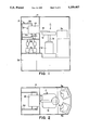
- FIG. 1 is a schematic partially sectional side view illustrating the surface treatment apparatus according to the present invention
- FIG. 2 is a top view illustrating the principal part of FIG. 1;
- FIG. 3 is a top view of the treatment tank used in the apparatus
- FIG. 4 is a side view thereof
- FIG. 5 is a vertical cross sectional view of the treatment tank.
- FIG. 6 is a cross sectional view of the lifting means provided under the treatment tank.
- FIG. 1 shows a schematic view of the surface treatment apparatus
- FIG. 2 is a top view thereof.
- a wafer holding mechanism 1, a supply/discharge section 2, wafer baskets 3a and 3b and a treatment section B that comprises the treatment or washing apparatus are all provided in a dust proof casing 4.
- the wafer holding mechanism 1 is comprised of a support body 1a, a shaft 1b, a stand 1c and a vacuum pad 1d.
- the vacuum pad 1d carries the semiconductor wafers.
- the rotatable shaft 1b is movable vertically on the support body 1a, and the stand 1c is mounted on the top end of the shaft 1b.
- the vacuum pad 1d is slidable on the stand 1c in a horizontal direction and holds a semiconductor wafer A stored in the wafer basket 3.
- the wafer holding mechanism 1 takes out the horizontally stored wafer A from the wafer basket 3a one by one with the use of suction pressure of the vacuum pad 1d and carries the wafer into treatment tank 10 of the treatment section B. After the treatment (washing, etc.), the wafer holding mechanism 1 takes out the treated wafer A from the treatment tank 10 and stores the wafer A in the wafer basket 3b.
- the supply/discharge section 2 includes filters 2a, pumps 2b, a tank 2c, pipes 2d and valves (not shown).
- the tank 2c includes several tanks for different treatment liquid (not shown).
- the connections between the treatment liquid tanks and the treatment tank 10 can be switched over by the valves.
- the treatment liquid stored in the tank 2c is filtered and supplied to the treatment tank 10 by a supply system of the supply/discharge section 2 at the same time as the operation of the supply system.
- the discharged wasted liquid is discharged into a predetermined reservoir or stored in the tank 2c after being filtered.
- the supply system can be partially or entirely switched to a discharge system by the valve operation.
- a supply system (not shown) for drying gas such as nitrogen is also provided.
- FIG. 5 shows the detail of the treatment section B.
- the treatment section B is comprised of the treatment tank 10, a movable wall 20, a piston cylinder mechanism 31, a first bellows 32 and a lift member 40.
- the treatment tank 10 is a cubic case 11, and a cover 13 is detachably fitted on top of the case 11. Inside the cubic case 11 is provided an inner casing 12 made of an anti-corrosion synthetic resin (registered trade mark "TEFLON").
- the inner casing 12 has a cubic shape on its outside, and the inside is cylindrical shape with a bottom.
- a circular recess 12b is coaxially (relative to the cylindrical inside of the inner casing) formed in the bottom wall of the inner casing 12. The diameter of the circular recess 12b is smaller than the diameter of the inner casing 12.
- a plurality of lower fluid holes P1 are provided in the recess 12b. These holes P1 are provided on a same circumferential circle with equal distance between them.
- a horizontally long opening 11a At a lower part of the side wall of the case 11 is provided a horizontally long opening 11a.
- an opening 12a is opened in the inner casing 12.
- the inner surface of the opening 11a of the case 11 is covered with anti-corrosion synthetic resin which forms a part of the inner casing 12.
- the movable wall 20 which is comprised of a circular wall body 21, a reinforcement plate 22 and a pressing plate 23, is tightly but slidably installed in the cylindrical inside of the inner casing 12.
- the movable wall 20 is moved like a piston.
- the circular wall body 21 that is made of anti-corrosion synthetic resin (registered trade mark "TEFLON") is reinforced by the reinforcement plate 22 which is a metallic circular ring and the pressing plate 23 fixed on the upper side of the reinforcement plate 22.
- TEFLON anti-corrosion synthetic resin
- a plurality of upper fluid holes P2 (three holes shown in FIG. 3) opened in the wall 20 are provided on a same circumferential circle with equal distance so that the holes P2 are positioned between two lower fluid holes P1.
- the fluid holes P1 and P2 are connected to the supply/discharge section 2 so as to supply the treatment liquid to the treatment tank 10.
- each upper and lower fluid holes P2 and P1 incline against the bottom surface of the recess 12b so that a circumferential component force is generated onto the semiconductor wafer by the ejection of the fluid.
- the first bellows 32 is made of corrosion resistance material.
- the bellows 32 is provided between the circumferential edge of the movable wall 20 and the top of the inner casing 12. Upper end portion of the first bellows 32 is held between the upper edge of the inner casing 12 and the cover 13. Thus, the cover 13 is securely fitted to the top of the inner casing 12.
- the lift member 40 is comprised of a lift body 41, a support pin 42, a second bellows 43, a connecting member 46 and a piston cylinder 48.
- the support pin 42 is provided in the lower fluid holes P1.
- the upper portion of the support pin 42 is supported by a first passage member 49a, and the lower portion of the support pin 42 is fixed to a second passage member 49b.
- the lift body 41 has the second bellows 43 and is provided so as to surround the lower fluid hole P1, and a connecting pipe 5 is fixed to the inside of the lift body 41.
- the lift body 41 is fitted to the connecting member 46 which is connected to the piston cylinder 48 by means of a reinforcement ring 45 and mounting nut 47.
- the upper part of the second bellows 43 is connected to the under surface of flange 44a of the inner casing 12 by a mounting plates 44b and 44c and bolt 44d.
- the vacuum pad 1d approaches the wafer basket 3a and holds a wafer A at the bottom end. At this time, the height of the vacuum pad 1d is adjusted so as to mate the number of wafers.
- the vacuum pad 1d holds the wafer A from the wafer basket 3a as shown by two dotted line in FIG. 2, and the vertical shaft 1b is rotated. As a result, the vacuum pad 1d rotates to the treatment section B and then adjusted the height. Thus, one wafer is moved to the front of the opening 11a of the treatment section B.
- the vacuum pad 1d is controlled to be extended towards the opening 11a and inserts the wafer A in the inner casing 12 through the opening 11a.
- vacuum holding by the vacuum pad 1d is released.
- the wafer A rests on the three support pins 42.
- the lift body and support pins 42 are moved downwardly, the wafer A is placed in the recess, the movable wall 20 moves down to the bottom of the inner casing 12, thus forming a closed room between the movable wall 20 and the recess 12b.
- washing of the wafer is performed.
- the washing is performed by supplying a first washing liquid (chemical liquid) from the supply/discharge section.
- the washing liquid is supplied through one or two lower fluid holes P1 and one or two upper fluid holes P2, and then the washing liquid discharged via the remaining fluid holes P1 and P2.
- the washing liquid is supplied with a pressure of about 2 Kg/cm 2 . Accordingly, the wafer floats from the bottom of the recess by being lifted by the liquid from the below and is also pressed down by the liquid from the above. Thus, the wafer keeps the floating state in the closed room without making contact with the upper surface of the recess 12b and the lower face of the movable wall 20. In this state, the wafer receives the fluid spout from the above and also from the below, thus being cleaned uniformly.
- the washing liquid is supplied from the inclined fluid holes in the direction which the circumferential component of a force is generated onto the wafer.
- the wafer is rotated by the liquid pressure supplied form the above and from the below.
- the top and bottom surfaces of the wafer are cleaned more uniformly, and a reduction of unevenness of washing and shortening of washing period are completed.
- the washing liquid discharged from the recess 12b is supplied to the filter 2a via pipes, and the filtered washing liquid is accommodated in the tank 2c, and then, pumped up by the pump 2b, returned to the treatment takn 10.
- the supply of the first washing liquid is stopped, and the washing liquid remaining inside the washing tank and on the wafer are removed.
- the supply system valves which supplied the washing liquid are switched over, and nitrogen gas is blown out via the supply system onto the wafer effectively while the wafer is rotated, and then the washing liquid is collected.
- a second washing liquid is supplied from the supply/discharge section for the next washing in the same manner as described above. Float and rotation of the wafer occurs in the same manner as the steps taken before.
- the washing liquid is collected, the wafer is rinsed with pure water and the water is discharged. This washing process is repeated for several times depending upon the object of the washing liquid, and then drying is performed successively.
- the movable wall 20 is moved upward, so that the recess is opened above the wafer.
- the lift body 41 is next moved upwardly by the cylinder 48, and the wafer is pushed up by the support pins 42.
- the vacuum pad 1d extends through the opening 11b to above the wafer, holds the wafer and carries out from the opening 11b, placing the thus washed wafer in the wafer basket 3b. The entire washing operation cycle is completed.
- the outside of the treatment tank 10 is about 300 mm in length and width and about 190 mm in height, for example. Also, if the wafer is about 0.5-1.5 mm in thickness, the recess 12b can be as shallow as 5-7 mm in depth. With such dimensions, even though the amount of the washing liquid supplied to the tank 10 is small in the amount, the washing liquid can wash the entire surface of the wafer thoroughly. Thus, a little amount of washing liquid can clean the wafer completely.
- a plurality of nozzles 51 and 52 for drying gas, such as nitrogen gas are provided in the recess 12b and the movable wall 20, respectively, so that the gas is evenly distributed.
- a part of the washing liquid supply/discharge system can be alternatively used as the gas system.
- the upper and lower fluid holes may be provided perpendicularly to the bottom of the recess 12b so that the wafer can be treated without rotation.
- the support pin 42 may be provided so as to penetrate the bottom of the recess 12b as an element to avoid using the lower fluid holes P1.
- the treatment tank is not required for every treatment process, as a result the entire apparatus can be small in size.
- the fluid is supplied to the small closed room and from which discharged through separate holes at the same time, and the wafer is treated one by one, then pure fluid is supplied always around the wafer, thus unevenness of treatment does not occur, rapid and certain treatment is performed even though the wafer is large in diameter.
- the wafer can keep the floating state in the treatment tank by the fluid pressure when it is being treated, and the fluid can flow around the both sides of the wafer, resulting in no unevenness of washing and high washing efficiency.
- the treatment tank can be compact, so that the washing liquid supplied into the washing tank can be utilized for washing operation without wasting it compared to prior art devices wherein the wafer is dipped in the washing liquid stored in the washing tank.
- an unevenness of washing is more reduced by rotating the wafer, and vacuum drying can be achieved by exhausting the gase from the recess.
- the wafer can be easily and certainly inserted into and taken out from the narrow recess in the treatment tank body, the chemical liquid remained in the penetrating part of the support pin can be eliminated by the drying gas, the leakage of fluid from the top end of the treatment tank body can be prevented, and the leakage of the fluid from the penetrating part of the support pin into the bottom of the tank body can be prevented.
Landscapes
- Cleaning Or Drying Semiconductors (AREA)
Abstract
Description
Claims (4)
Applications Claiming Priority (2)
| Application Number | Priority Date | Filing Date | Title |
|---|---|---|---|
| JP2-155471 | 1990-06-15 | ||
| JP15547190 | 1990-06-15 |
Publications (1)
| Publication Number | Publication Date |
|---|---|
| US5259407A true US5259407A (en) | 1993-11-09 |
Family
ID=15606780
Family Applications (1)
| Application Number | Title | Priority Date | Filing Date |
|---|---|---|---|
| US07/715,421 Expired - Fee Related US5259407A (en) | 1990-06-15 | 1991-06-14 | Surface treatment method and apparatus for a semiconductor wafer |
Country Status (1)
| Country | Link |
|---|---|
| US (1) | US5259407A (en) |
Cited By (57)
| Publication number | Priority date | Publication date | Assignee | Title |
|---|---|---|---|---|
| WO1997014178A1 (en) * | 1995-10-13 | 1997-04-17 | Ziying Wen | Method and apparatus for chemical processing semiconductor wafers |
| US5785068A (en) * | 1995-05-11 | 1998-07-28 | Dainippon Screen Mfg. Co., Ltd. | Substrate spin cleaning apparatus |
| US6113771A (en) * | 1998-04-21 | 2000-09-05 | Applied Materials, Inc. | Electro deposition chemistry |
| WO2000059010A1 (en) * | 1999-03-31 | 2000-10-05 | Lam Research Corporation | Sealing techniques suitable for different geometries and constrained spaces |
| US6136163A (en) * | 1999-03-05 | 2000-10-24 | Applied Materials, Inc. | Apparatus for electro-chemical deposition with thermal anneal chamber |
| US6228233B1 (en) | 1998-11-30 | 2001-05-08 | Applied Materials, Inc. | Inflatable compliant bladder assembly |
| US6254760B1 (en) | 1999-03-05 | 2001-07-03 | Applied Materials, Inc. | Electro-chemical deposition system and method |
| US6258220B1 (en) | 1998-11-30 | 2001-07-10 | Applied Materials, Inc. | Electro-chemical deposition system |
| US6261433B1 (en) | 1998-04-21 | 2001-07-17 | Applied Materials, Inc. | Electro-chemical deposition system and method of electroplating on substrates |
| US6267853B1 (en) | 1999-07-09 | 2001-07-31 | Applied Materials, Inc. | Electro-chemical deposition system |
| US6290865B1 (en) | 1998-11-30 | 2001-09-18 | Applied Materials, Inc. | Spin-rinse-drying process for electroplated semiconductor wafers |
| US20020037641A1 (en) * | 1998-06-01 | 2002-03-28 | Ritzdorf Thomas L. | Method and apparatus for low temperature annealing of metallization micro-structure in the production of a microelectronic device |
| US6379522B1 (en) | 1999-01-11 | 2002-04-30 | Applied Materials, Inc. | Electrodeposition chemistry for filling of apertures with reflective metal |
| US6416647B1 (en) | 1998-04-21 | 2002-07-09 | Applied Materials, Inc. | Electro-chemical deposition cell for face-up processing of single semiconductor substrates |
| US6423636B1 (en) * | 1999-11-19 | 2002-07-23 | Applied Materials, Inc. | Process sequence for improved seed layer productivity and achieving 3mm edge exclusion for a copper metalization process on semiconductor wafer |
| US20020113039A1 (en) * | 1999-07-09 | 2002-08-22 | Mok Yeuk-Fai Edwin | Integrated semiconductor substrate bevel cleaning apparatus and method |
| US20020112964A1 (en) * | 2000-07-12 | 2002-08-22 | Applied Materials, Inc. | Process window for gap-fill on very high aspect ratio structures using additives in low acid copper baths |
| US6478937B2 (en) | 2001-01-19 | 2002-11-12 | Applied Material, Inc. | Substrate holder system with substrate extension apparatus and associated method |
| US6508920B1 (en) | 1998-02-04 | 2003-01-21 | Semitool, Inc. | Apparatus for low-temperature annealing of metallization microstructures in the production of a microelectronic device |
| US6516815B1 (en) | 1999-07-09 | 2003-02-11 | Applied Materials, Inc. | Edge bead removal/spin rinse dry (EBR/SRD) module |
| US6544399B1 (en) | 1999-01-11 | 2003-04-08 | Applied Materials, Inc. | Electrodeposition chemistry for filling apertures with reflective metal |
| US6551488B1 (en) | 1999-04-08 | 2003-04-22 | Applied Materials, Inc. | Segmenting of processing system into wet and dry areas |
| US6551484B2 (en) | 1999-04-08 | 2003-04-22 | Applied Materials, Inc. | Reverse voltage bias for electro-chemical plating system and method |
| US6557237B1 (en) | 1999-04-08 | 2003-05-06 | Applied Materials, Inc. | Removable modular cell for electro-chemical plating and method |
| US6571657B1 (en) | 1999-04-08 | 2003-06-03 | Applied Materials Inc. | Multiple blade robot adjustment apparatus and associated method |
| US6576110B2 (en) | 2000-07-07 | 2003-06-10 | Applied Materials, Inc. | Coated anode apparatus and associated method |
| US6582578B1 (en) | 1999-04-08 | 2003-06-24 | Applied Materials, Inc. | Method and associated apparatus for tilting a substrate upon entry for metal deposition |
| US6585876B2 (en) | 1999-04-08 | 2003-07-01 | Applied Materials Inc. | Flow diffuser to be used in electro-chemical plating system and method |
| US6610189B2 (en) | 2001-01-03 | 2003-08-26 | Applied Materials, Inc. | Method and associated apparatus to mechanically enhance the deposition of a metal film within a feature |
| US20030201184A1 (en) * | 1999-04-08 | 2003-10-30 | Applied Materials, Inc. | Method and associated apparatus for tilting a substrate upon entry for metal deposition |
| US20030201166A1 (en) * | 2002-04-29 | 2003-10-30 | Applied Materials, Inc. | method for regulating the electrical power applied to a substrate during an immersion process |
| US20030209443A1 (en) * | 2002-05-09 | 2003-11-13 | Applied Materials, Inc. | Substrate support with fluid retention band |
| US6662673B1 (en) | 1999-04-08 | 2003-12-16 | Applied Materials, Inc. | Linear motion apparatus and associated method |
| US20040003873A1 (en) * | 1999-03-05 | 2004-01-08 | Applied Materials, Inc. | Method and apparatus for annealing copper films |
| US20040079633A1 (en) * | 2000-07-05 | 2004-04-29 | Applied Materials, Inc. | Apparatus for electro chemical deposition of copper metallization with the capability of in-situ thermal annealing |
| US6770565B2 (en) | 2002-01-08 | 2004-08-03 | Applied Materials Inc. | System for planarizing metal conductive layers |
| US20040149573A1 (en) * | 2003-01-31 | 2004-08-05 | Applied Materials, Inc. | Contact ring with embedded flexible contacts |
| US20040154185A1 (en) * | 1997-07-10 | 2004-08-12 | Applied Materials, Inc. | Method and apparatus for heating and cooling substrates |
| US20040200725A1 (en) * | 2003-04-09 | 2004-10-14 | Applied Materials Inc. | Application of antifoaming agent to reduce defects in a semiconductor electrochemical plating process |
| US6806186B2 (en) | 1998-02-04 | 2004-10-19 | Semitool, Inc. | Submicron metallization using electrochemical deposition |
| US20040206628A1 (en) * | 2003-04-18 | 2004-10-21 | Applied Materials, Inc. | Electrical bias during wafer exit from electrolyte bath |
| US20040209414A1 (en) * | 2003-04-18 | 2004-10-21 | Applied Materials, Inc. | Two position anneal chamber |
| US6808612B2 (en) | 2000-05-23 | 2004-10-26 | Applied Materials, Inc. | Method and apparatus to overcome anomalies in copper seed layers and to tune for feature size and aspect ratio |
| US6824612B2 (en) | 2001-12-26 | 2004-11-30 | Applied Materials, Inc. | Electroless plating system |
| US6837978B1 (en) | 1999-04-08 | 2005-01-04 | Applied Materials, Inc. | Deposition uniformity control for electroplating apparatus, and associated method |
| US20050092602A1 (en) * | 2003-10-29 | 2005-05-05 | Harald Herchen | Electrochemical plating cell having a membrane stack |
| US20050092601A1 (en) * | 2003-10-29 | 2005-05-05 | Harald Herchen | Electrochemical plating cell having a diffusion member |
| US6913680B1 (en) | 2000-05-02 | 2005-07-05 | Applied Materials, Inc. | Method of application of electrical biasing to enhance metal deposition |
| US20050218000A1 (en) * | 2004-04-06 | 2005-10-06 | Applied Materials, Inc. | Conditioning of contact leads for metal plating systems |
| DE10255231B4 (en) * | 2002-11-26 | 2006-02-02 | Uhde High Pressure Technologies Gmbh | High pressure device for closing a pressure vessel in the clean room |
| US7025861B2 (en) | 2003-02-06 | 2006-04-11 | Applied Materials | Contact plating apparatus |
| US20060102467A1 (en) * | 2004-11-15 | 2006-05-18 | Harald Herchen | Current collimation for thin seed and direct plating |
| US7094291B2 (en) | 1990-05-18 | 2006-08-22 | Semitool, Inc. | Semiconductor processing apparatus |
| US7285195B2 (en) | 2004-06-24 | 2007-10-23 | Applied Materials, Inc. | Electric field reducing thrust plate |
| US7399713B2 (en) | 1998-03-13 | 2008-07-15 | Semitool, Inc. | Selective treatment of microelectric workpiece surfaces |
| US7654221B2 (en) | 2003-10-06 | 2010-02-02 | Applied Materials, Inc. | Apparatus for electroless deposition of metals onto semiconductor substrates |
| CN103286086A (en) * | 2012-03-05 | 2013-09-11 | 无锡华润华晶微电子有限公司 | Wafer cleaning method and device |
Citations (4)
| Publication number | Priority date | Publication date | Assignee | Title |
|---|---|---|---|---|
| US4736758A (en) * | 1985-04-15 | 1988-04-12 | Wacom Co., Ltd. | Vapor drying apparatus |
| JPH01270933A (en) * | 1988-04-25 | 1989-10-30 | Hitachi Ltd | Device for treatment under reduced pressure |
| US4922277A (en) * | 1988-11-28 | 1990-05-01 | The United States Of America As Represented By The Secretary Of The Air Force | Silicon wafer photoresist developer |
| US5169408A (en) * | 1990-01-26 | 1992-12-08 | Fsi International, Inc. | Apparatus for wafer processing with in situ rinse |
-
1991
- 1991-06-14 US US07/715,421 patent/US5259407A/en not_active Expired - Fee Related
Patent Citations (5)
| Publication number | Priority date | Publication date | Assignee | Title |
|---|---|---|---|---|
| US4736758A (en) * | 1985-04-15 | 1988-04-12 | Wacom Co., Ltd. | Vapor drying apparatus |
| US4777970A (en) * | 1985-04-15 | 1988-10-18 | Wacom Co., Ltd. | Vapor drying apparatus |
| JPH01270933A (en) * | 1988-04-25 | 1989-10-30 | Hitachi Ltd | Device for treatment under reduced pressure |
| US4922277A (en) * | 1988-11-28 | 1990-05-01 | The United States Of America As Represented By The Secretary Of The Air Force | Silicon wafer photoresist developer |
| US5169408A (en) * | 1990-01-26 | 1992-12-08 | Fsi International, Inc. | Apparatus for wafer processing with in situ rinse |
Cited By (77)
| Publication number | Priority date | Publication date | Assignee | Title |
|---|---|---|---|---|
| US7138016B2 (en) | 1990-05-18 | 2006-11-21 | Semitool, Inc. | Semiconductor processing apparatus |
| US7094291B2 (en) | 1990-05-18 | 2006-08-22 | Semitool, Inc. | Semiconductor processing apparatus |
| US5785068A (en) * | 1995-05-11 | 1998-07-28 | Dainippon Screen Mfg. Co., Ltd. | Substrate spin cleaning apparatus |
| WO1997014178A1 (en) * | 1995-10-13 | 1997-04-17 | Ziying Wen | Method and apparatus for chemical processing semiconductor wafers |
| US6239038B1 (en) | 1995-10-13 | 2001-05-29 | Ziying Wen | Method for chemical processing semiconductor wafers |
| US20040154185A1 (en) * | 1997-07-10 | 2004-08-12 | Applied Materials, Inc. | Method and apparatus for heating and cooling substrates |
| US6929774B2 (en) | 1997-07-10 | 2005-08-16 | Applied Materials, Inc. | Method and apparatus for heating and cooling substrates |
| US6508920B1 (en) | 1998-02-04 | 2003-01-21 | Semitool, Inc. | Apparatus for low-temperature annealing of metallization microstructures in the production of a microelectronic device |
| US6806186B2 (en) | 1998-02-04 | 2004-10-19 | Semitool, Inc. | Submicron metallization using electrochemical deposition |
| US7144805B2 (en) | 1998-02-04 | 2006-12-05 | Semitool, Inc. | Method of submicron metallization using electrochemical deposition of recesses including a first deposition at a first current density and a second deposition at an increased current density |
| US7462269B2 (en) | 1998-02-04 | 2008-12-09 | Semitool, Inc. | Method for low temperature annealing of metallization micro-structures in the production of a microelectronic device |
| US7399713B2 (en) | 1998-03-13 | 2008-07-15 | Semitool, Inc. | Selective treatment of microelectric workpiece surfaces |
| USRE40218E1 (en) * | 1998-04-21 | 2008-04-08 | Uziel Landau | Electro-chemical deposition system and method of electroplating on substrates |
| US6350366B1 (en) | 1998-04-21 | 2002-02-26 | Applied Materials, Inc. | Electro deposition chemistry |
| US6261433B1 (en) | 1998-04-21 | 2001-07-17 | Applied Materials, Inc. | Electro-chemical deposition system and method of electroplating on substrates |
| US6416647B1 (en) | 1998-04-21 | 2002-07-09 | Applied Materials, Inc. | Electro-chemical deposition cell for face-up processing of single semiconductor substrates |
| US6610191B2 (en) | 1998-04-21 | 2003-08-26 | Applied Materials, Inc. | Electro deposition chemistry |
| US6113771A (en) * | 1998-04-21 | 2000-09-05 | Applied Materials, Inc. | Electro deposition chemistry |
| US6994776B2 (en) * | 1998-06-01 | 2006-02-07 | Semitool Inc. | Method and apparatus for low temperature annealing of metallization micro-structure in the production of a microelectronic device |
| US20020037641A1 (en) * | 1998-06-01 | 2002-03-28 | Ritzdorf Thomas L. | Method and apparatus for low temperature annealing of metallization micro-structure in the production of a microelectronic device |
| US6290865B1 (en) | 1998-11-30 | 2001-09-18 | Applied Materials, Inc. | Spin-rinse-drying process for electroplated semiconductor wafers |
| US6258220B1 (en) | 1998-11-30 | 2001-07-10 | Applied Materials, Inc. | Electro-chemical deposition system |
| US6635157B2 (en) | 1998-11-30 | 2003-10-21 | Applied Materials, Inc. | Electro-chemical deposition system |
| US6228233B1 (en) | 1998-11-30 | 2001-05-08 | Applied Materials, Inc. | Inflatable compliant bladder assembly |
| US6379522B1 (en) | 1999-01-11 | 2002-04-30 | Applied Materials, Inc. | Electrodeposition chemistry for filling of apertures with reflective metal |
| US6596151B2 (en) | 1999-01-11 | 2003-07-22 | Applied Materials, Inc. | Electrodeposition chemistry for filling of apertures with reflective metal |
| US6544399B1 (en) | 1999-01-11 | 2003-04-08 | Applied Materials, Inc. | Electrodeposition chemistry for filling apertures with reflective metal |
| US7192494B2 (en) | 1999-03-05 | 2007-03-20 | Applied Materials, Inc. | Method and apparatus for annealing copper films |
| US20040003873A1 (en) * | 1999-03-05 | 2004-01-08 | Applied Materials, Inc. | Method and apparatus for annealing copper films |
| US6136163A (en) * | 1999-03-05 | 2000-10-24 | Applied Materials, Inc. | Apparatus for electro-chemical deposition with thermal anneal chamber |
| US6254760B1 (en) | 1999-03-05 | 2001-07-03 | Applied Materials, Inc. | Electro-chemical deposition system and method |
| US6536777B2 (en) | 1999-03-31 | 2003-03-25 | Lam Research Corporation | Sealing techniques suitable for different geometries and constrained spaces |
| WO2000059010A1 (en) * | 1999-03-31 | 2000-10-05 | Lam Research Corporation | Sealing techniques suitable for different geometries and constrained spaces |
| US6557237B1 (en) | 1999-04-08 | 2003-05-06 | Applied Materials, Inc. | Removable modular cell for electro-chemical plating and method |
| US6837978B1 (en) | 1999-04-08 | 2005-01-04 | Applied Materials, Inc. | Deposition uniformity control for electroplating apparatus, and associated method |
| US6585876B2 (en) | 1999-04-08 | 2003-07-01 | Applied Materials Inc. | Flow diffuser to be used in electro-chemical plating system and method |
| US20030201184A1 (en) * | 1999-04-08 | 2003-10-30 | Applied Materials, Inc. | Method and associated apparatus for tilting a substrate upon entry for metal deposition |
| US6582578B1 (en) | 1999-04-08 | 2003-06-24 | Applied Materials, Inc. | Method and associated apparatus for tilting a substrate upon entry for metal deposition |
| US6551488B1 (en) | 1999-04-08 | 2003-04-22 | Applied Materials, Inc. | Segmenting of processing system into wet and dry areas |
| US6551484B2 (en) | 1999-04-08 | 2003-04-22 | Applied Materials, Inc. | Reverse voltage bias for electro-chemical plating system and method |
| US6662673B1 (en) | 1999-04-08 | 2003-12-16 | Applied Materials, Inc. | Linear motion apparatus and associated method |
| US6571657B1 (en) | 1999-04-08 | 2003-06-03 | Applied Materials Inc. | Multiple blade robot adjustment apparatus and associated method |
| US20030168346A1 (en) * | 1999-04-08 | 2003-09-11 | Applied Materials, Inc. | Segmenting of processing system into wet and dry areas |
| US6516815B1 (en) | 1999-07-09 | 2003-02-11 | Applied Materials, Inc. | Edge bead removal/spin rinse dry (EBR/SRD) module |
| US20030213772A9 (en) * | 1999-07-09 | 2003-11-20 | Mok Yeuk-Fai Edwin | Integrated semiconductor substrate bevel cleaning apparatus and method |
| US20020113039A1 (en) * | 1999-07-09 | 2002-08-22 | Mok Yeuk-Fai Edwin | Integrated semiconductor substrate bevel cleaning apparatus and method |
| US6267853B1 (en) | 1999-07-09 | 2001-07-31 | Applied Materials, Inc. | Electro-chemical deposition system |
| US6423636B1 (en) * | 1999-11-19 | 2002-07-23 | Applied Materials, Inc. | Process sequence for improved seed layer productivity and achieving 3mm edge exclusion for a copper metalization process on semiconductor wafer |
| US6913680B1 (en) | 2000-05-02 | 2005-07-05 | Applied Materials, Inc. | Method of application of electrical biasing to enhance metal deposition |
| US6808612B2 (en) | 2000-05-23 | 2004-10-26 | Applied Materials, Inc. | Method and apparatus to overcome anomalies in copper seed layers and to tune for feature size and aspect ratio |
| US20040079633A1 (en) * | 2000-07-05 | 2004-04-29 | Applied Materials, Inc. | Apparatus for electro chemical deposition of copper metallization with the capability of in-situ thermal annealing |
| US6576110B2 (en) | 2000-07-07 | 2003-06-10 | Applied Materials, Inc. | Coated anode apparatus and associated method |
| US20020112964A1 (en) * | 2000-07-12 | 2002-08-22 | Applied Materials, Inc. | Process window for gap-fill on very high aspect ratio structures using additives in low acid copper baths |
| US6610189B2 (en) | 2001-01-03 | 2003-08-26 | Applied Materials, Inc. | Method and associated apparatus to mechanically enhance the deposition of a metal film within a feature |
| US6478937B2 (en) | 2001-01-19 | 2002-11-12 | Applied Material, Inc. | Substrate holder system with substrate extension apparatus and associated method |
| US6824612B2 (en) | 2001-12-26 | 2004-11-30 | Applied Materials, Inc. | Electroless plating system |
| US6770565B2 (en) | 2002-01-08 | 2004-08-03 | Applied Materials Inc. | System for planarizing metal conductive layers |
| US6911136B2 (en) | 2002-04-29 | 2005-06-28 | Applied Materials, Inc. | Method for regulating the electrical power applied to a substrate during an immersion process |
| US20030201166A1 (en) * | 2002-04-29 | 2003-10-30 | Applied Materials, Inc. | method for regulating the electrical power applied to a substrate during an immersion process |
| US7189313B2 (en) | 2002-05-09 | 2007-03-13 | Applied Materials, Inc. | Substrate support with fluid retention band |
| US20030209443A1 (en) * | 2002-05-09 | 2003-11-13 | Applied Materials, Inc. | Substrate support with fluid retention band |
| DE10255231B4 (en) * | 2002-11-26 | 2006-02-02 | Uhde High Pressure Technologies Gmbh | High pressure device for closing a pressure vessel in the clean room |
| US20040149573A1 (en) * | 2003-01-31 | 2004-08-05 | Applied Materials, Inc. | Contact ring with embedded flexible contacts |
| US7087144B2 (en) | 2003-01-31 | 2006-08-08 | Applied Materials, Inc. | Contact ring with embedded flexible contacts |
| US7025861B2 (en) | 2003-02-06 | 2006-04-11 | Applied Materials | Contact plating apparatus |
| US20060124468A1 (en) * | 2003-02-06 | 2006-06-15 | Applied Materials, Inc. | Contact plating apparatus |
| US20040200725A1 (en) * | 2003-04-09 | 2004-10-14 | Applied Materials Inc. | Application of antifoaming agent to reduce defects in a semiconductor electrochemical plating process |
| US20040206628A1 (en) * | 2003-04-18 | 2004-10-21 | Applied Materials, Inc. | Electrical bias during wafer exit from electrolyte bath |
| US7311810B2 (en) | 2003-04-18 | 2007-12-25 | Applied Materials, Inc. | Two position anneal chamber |
| US20040209414A1 (en) * | 2003-04-18 | 2004-10-21 | Applied Materials, Inc. | Two position anneal chamber |
| US7654221B2 (en) | 2003-10-06 | 2010-02-02 | Applied Materials, Inc. | Apparatus for electroless deposition of metals onto semiconductor substrates |
| US20050092602A1 (en) * | 2003-10-29 | 2005-05-05 | Harald Herchen | Electrochemical plating cell having a membrane stack |
| US20050092601A1 (en) * | 2003-10-29 | 2005-05-05 | Harald Herchen | Electrochemical plating cell having a diffusion member |
| US20050218000A1 (en) * | 2004-04-06 | 2005-10-06 | Applied Materials, Inc. | Conditioning of contact leads for metal plating systems |
| US7285195B2 (en) | 2004-06-24 | 2007-10-23 | Applied Materials, Inc. | Electric field reducing thrust plate |
| US20060102467A1 (en) * | 2004-11-15 | 2006-05-18 | Harald Herchen | Current collimation for thin seed and direct plating |
| CN103286086A (en) * | 2012-03-05 | 2013-09-11 | 无锡华润华晶微电子有限公司 | Wafer cleaning method and device |
Similar Documents
| Publication | Publication Date | Title |
|---|---|---|
| US5259407A (en) | Surface treatment method and apparatus for a semiconductor wafer | |
| KR100271772B1 (en) | Semiconductor Wet Etching Equipment | |
| US5556479A (en) | Method and apparatus for drying semiconductor wafers | |
| US6374837B2 (en) | Single semiconductor wafer processor | |
| US6895979B2 (en) | Processing apparatus and processing method | |
| US20060237054A1 (en) | Apparatus and method for washing quartz parts, particularly for process equipment used in semiconductor industries | |
| KR20200089060A (en) | Substrate drying chamber | |
| JP3341727B2 (en) | Wet equipment | |
| US6492284B2 (en) | Reactor for processing a workpiece using sonic energy | |
| WO2003006183A2 (en) | Method and apparatus for cleaning semiconductor wafers and other flat media | |
| JPH04253332A (en) | Semiconductor wafer treating device | |
| KR101052821B1 (en) | Substrate processing apparatus and method | |
| US6511914B2 (en) | Reactor for processing a workpiece using sonic energy | |
| JP3910757B2 (en) | Processing apparatus and processing method | |
| JP2965876B2 (en) | Substrate processing apparatus and processing tank used therein | |
| JPH073817B2 (en) | Surface treatment equipment for semiconductor wafers | |
| JP2002370071A (en) | Washing apparatus | |
| JPH08141526A (en) | Substrate treatment apparatus and treatment tank used therein | |
| KR20010040938A (en) | Device for processing wafer | |
| KR100695233B1 (en) | Substrate Cleaning Apparatus and Method | |
| KR200181400Y1 (en) | Wet Semiconductor Etch Cleaning Rinsing Equipment | |
| TWI725745B (en) | Substrate drying chamber | |
| JPH10163158A (en) | Cleaning apparatus for sheetlike body | |
| KR100481157B1 (en) | Method and apparatus for drying a substrate | |
| KR20080096065A (en) | Substrate Cleaning Apparatus and Method |
Legal Events
| Date | Code | Title | Description |
|---|---|---|---|
| AS | Assignment |
Owner name: MATRIX INC., JAPAN Free format text: ASSIGNMENT OF ASSIGNORS INTEREST.;ASSIGNORS:TUCHIDA, JUNICHI;TAKAMATSU, TOSHIYUKI;REEL/FRAME:005747/0191 Effective date: 19910607 |
|
| AS | Assignment |
Owner name: MATRIX INC., JAPAN Free format text: 1CHANGE OF ADDRESS OF ASSIGNEE;ASSIGNOR:MATRIX INC.;REEL/FRAME:006667/0837 Effective date: 19921022 |
|
| REMI | Maintenance fee reminder mailed | ||
| LAPS | Lapse for failure to pay maintenance fees | ||
| FP | Lapsed due to failure to pay maintenance fee |
Effective date: 19971112 |
|
| FEPP | Fee payment procedure |
Free format text: PAYOR NUMBER ASSIGNED (ORIGINAL EVENT CODE: ASPN); ENTITY STATUS OF PATENT OWNER: LARGE ENTITY |
|
| STCH | Information on status: patent discontinuation |
Free format text: PATENT EXPIRED DUE TO NONPAYMENT OF MAINTENANCE FEES UNDER 37 CFR 1.362 |