US5073798A - Electronic photography apparatus - Google Patents
Electronic photography apparatus Download PDFInfo
- Publication number
- US5073798A US5073798A US07/625,886 US62588690A US5073798A US 5073798 A US5073798 A US 5073798A US 62588690 A US62588690 A US 62588690A US 5073798 A US5073798 A US 5073798A
- Authority
- US
- United States
- Prior art keywords
- developers
- developing
- spacing
- photoconductor material
- latent image
- Prior art date
- Legal status (The legal status is an assumption and is not a legal conclusion. Google has not performed a legal analysis and makes no representation as to the accuracy of the status listed.)
- Expired - Fee Related
Links
Images

Classifications
-
- G—PHYSICS
- G03—PHOTOGRAPHY; CINEMATOGRAPHY; ANALOGOUS TECHNIQUES USING WAVES OTHER THAN OPTICAL WAVES; ELECTROGRAPHY; HOLOGRAPHY
- G03G—ELECTROGRAPHY; ELECTROPHOTOGRAPHY; MAGNETOGRAPHY
- G03G15/00—Apparatus for electrographic processes using a charge pattern
- G03G15/06—Apparatus for electrographic processes using a charge pattern for developing
- G03G15/10—Apparatus for electrographic processes using a charge pattern for developing using a liquid developer
- G03G15/11—Removing excess liquid developer, e.g. by heat
-
- G—PHYSICS
- G03—PHOTOGRAPHY; CINEMATOGRAPHY; ANALOGOUS TECHNIQUES USING WAVES OTHER THAN OPTICAL WAVES; ELECTROGRAPHY; HOLOGRAPHY
- G03G—ELECTROGRAPHY; ELECTROPHOTOGRAPHY; MAGNETOGRAPHY
- G03G15/00—Apparatus for electrographic processes using a charge pattern
- G03G15/06—Apparatus for electrographic processes using a charge pattern for developing
- G03G15/10—Apparatus for electrographic processes using a charge pattern for developing using a liquid developer
- G03G15/101—Apparatus for electrographic processes using a charge pattern for developing using a liquid developer for wetting the recording material
Definitions
- the present invention relates generally to electronic photography apparatus and, more particularly, to an electronic photography apparatus suitable for use in developing an electrostatic latent image in an electronic photography process or similar process.
- an electrostatic latent image is formed in such a manner that a photoconductive material such as a photoconductor is uniformly electrified (charged) and then selectively illuminated by a light in accordance with an image signal, so that charges on the portion illuminated by the light are extinguished.
- a dielectric material such as a paper, a plastic film or similar element is electrified by an electrostatic electrode called a multistylus head in response to an image signal, thereby forming an electrostatic latent image.
- a toner or developer charged to the polarity opposite to that of the electrostatic latent image carrier (photoconductor drum, dielectric film and so on) having the electrostatic latent image is electrostatically deposited on the electrified portion of the photoconductor drum and then developed.
- a dry type developing system using a dry developer and a wet type developing system using liquid developer are known.
- the dry developer is generally formed of very small particle powders. For this reason, if the dry developer is scattered, a problem of environmental disruption occurs.
- a developer cartridge in which the dry developer is accommodated should be constructed as a sealed type.
- Today, most of the developing apparatus are of such a type that an electrostatic latent image carrier that the developing portion are wholly removed and replaced. Therefore, this type of developing apparatus is expensive but the dry developer is excellent in preservation and if the developer is accommodated within the developer cartridge, it is easy to handle.
- the liquid developer is formed by dispersing into an insulating liquid powders of colorant such as dye stuff and the like.
- the liquid developer is injected from the developer container through the slit of a developing electrode used to charge the electrostatic latent image to the polarity opposite to that of the electrostatic latent image carrier, whereby colored particle powders are electrostatically deposited on the electrostatic latent image carrier.
- extra liquid developers which are not deposited on the electrostatic latent image carrier, are returned to and accommodated again within the developer container, rendering the colorant powders in the liquid developers low in concentration. This makes control of the concentration of the developing liquid (liquid developer) difficult.
- this electrostatic latent image developing method is characterized by a developer (i.e. toner) which is formed by a colorant dispersed into an electrostatic insulating organic material that is solid at normal temperature and when heated is changed into liquid, in which an electrostatic latent image is developed by the thus liquefied developer in a wet developing fashion.
- a developer i.e. toner
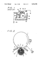
- FIG. 1. shows a cross-sectional view of a conventional developing apparatus that is described, for example, in Japanese Patent Published Gazette No. 64-6462.
- reference numeral 30 designates supporting portions 31 a photoconductor film extended between the supporting portions 30, 32 a preserving tank, 33 a developing liquid preserved in this preserving tank 32, 34 a developing roller, 35 a liquid lifting member, 36 an injection opening portion, 37 a developing electrode, 38 a spring and 39 a bias voltage source.
- the developing liquid 33 from the preserving tank 32 is lifted by the rotation of the developing roller 34 via the liquid lifting member 35, injected from the injection opening portion 36 and is filled in the space between the developing electrode 37 and the photoconductor film 31 for development. After the development, the developing liquid 33 is returned to the preserving tank 32 and subsequently utilized several times for the development.
- an electronic photography apparatus is comprised of a photoconductor material on which an electrostatic latent image is formed, a developing device for developing the electrostatic latent image formed on the photoconductor material, a developing electrode provided in the developing device for developing the electrostatic latent image, a means for supplying developers such that the developers exist in a spacing between the photoconductor material and the developing electrode, and an injection means for injecting air to the developers existing at the spacing between the photoconductor material and the developing electrode.
- an electronic photography apparatus is comprised of a photoconductor material on which an electrostatic latent image is formed, a developing device for developing the electrostatic latent image formed on the photoconductor material, a developing electrode provided in the developing device for developing the electrostatic latent image, a developer supplying container for storing therein developers supplied to the spacing between the photoconductor material and the developing electrode, a developer discharging container for storing therein developers discharged from the spacing between the photoconductor material and the developing electrode, and a circulating path provided independently of the two containers for supplying the developers to the spacing between the photoconductor material and the developing electrode.
- FIG. 1 is a diagrammatic view of a section illustrating an example of a conventional developing apparatus utilized in an electronic photography apparatus
- FIG. 2 is a schematic diagram showing a first embodiment of an electronic photography apparatus according to the present invention
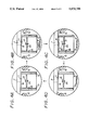
- FIGS. 3A-3D are schematic diagrams each showing a main portion of the electronic photography apparatus of FIG. 2 in an enlarged scale, respectively;
- FIGS. 4A-4D are schematic diagrams each showing a main portion of a second embodiment of the electronic photography apparatus according to the present invention, respectively.
- FIG. 2 and FIGS. 3A-3D a first embodiment of the electronic photography apparatus according to the present invention will be described hereinafter.
- a photoconductor drum 1 having a photoconductor material (such as a base material that can carry an electrostatic latent image) is wrapped around a cylindrical-shaped circumferential surface of the drum 1.
- a charging device 2 is provided to uniformly charge the entire surface of the photoconductor material on the drum 1 in, for example, negative charges.
- a semiconductor laser (light exposure system) 3 is provided to selectively illuminate the surface of the photoconductor material on the drum 1 with a laser beam in response to a video signal so that charges at the portion illuminated by the laser beam are erased to form an electrostatic latent image.
- a developer tank 4 contains therein solid developers.
- Reference numeral 5 designates particles of solid developers that are which are not yet used and 6 designates particle solid developers used.
- Reference numeral 7 designates an isolation member which is rotatable and 8 a stationary wall which incorporates therein a heater (not shown) to liquefy (melt) the solid developers 5 by the heating-process.
- Reference numeral 9 designates an inlet through which the solid developers 5 are supplied and 10 an outlet from which waste solid developers 6 are discharged.
- Reference numeral 11 designates a developing electrode which charges the solid developers 5 in polarity opposite to that of the photoconductor material.
- Reference numerals 12 and 13 designate nozzles from which air is injected to remove solid developers remaining in a narrow spacing between the photoconductor drum 1 and the developing electrode 11 by air pressure at the completion of the developing process.
- Liquid developer in which the particles of solid developers are heated by the heater and liquefied is supplied through the inlet 9 so as to fill in the narrow spacing between the photoconductor drum 1 and the developing electrode 11 for carrying out the developing process.
- the liquid developer remaining at the above-described narrow spacing can be prevented from being exhausted due to its surface tension. Accordingly, the remaining liquid developers can be discharged and collected by supplying the air from the air nozzles 12 and 13 to the spacing after the developing process.
- FIGS. 3A-3D show the main portion of the present invention, i.e. the portion near the developing electrode 11 in FIG. 2, in an enlarged scale, respectively.
- the liquid developer is supplied from the inlet 9 and filled into a narrow spacing 14 between the photoconductor drum 1 and the developing electrode 11 as shown in FIG. 3B.
- the developing process is carried out under this condition (see FIG. 3C). Even when the supply of liquid developer is stopped, or even when a valve 15 is opened to open the outlet 10 after the developing process is ended, the liquid developer remaining at the spacing 14 is not discharged due to its surface tension. Accordingly, when the air is injected to the spacing 14 from the air nozzles 12 and 13, the remaining liquid developer is discharged to the direction of the outlet 10 (FIG. 3D).
- the service life of the photoconductor material, the developing electrode and the like can be increased.
- FIGS. 4A-4D show a second embodiment of the electronic photography apparatus according to the present invention.
- like parts corresponding to those of FIG. 2 and FIGS. 3A to 3D are marked with the same references and therefore need not be described in detail.
- a circulating path 20 is coupled between the discharging path and the supplying path so that the toner (developer) flows through the circulating path 20 only in one direction.
- a pump 21 is provided in the intermediate portion of the circulating path 20 so as to force the solid developer remaining at the spacing 14 to be circulated, whereby the solid developer remaining at that spacing 14 is discharged to the outside of the apparatus at every developing process.
- the developer may be used two to three times if the composition thereof is not unsatisfactory
- air is supplied to the spacing 14 from the nozzles 12 and 13 to thereby discharge the circulated developer (FIG. 4D).
- the circulating path through which the developer is supplied to the spacing between the photoconductor portion and the developing electrode is provided in the path independently of the developer supplying and exhausting tanks and the developer is forced to be circulated through this circulating path, it becomes possible to perform uniform development using only a very small amount of the developer.
- solid developer supplying container and the solid developer discharging container are formed as a unitary body in the above-described embodiment, they may be provided independently.
- the electronic photography apparatus is comprised of the photoconductor material on which an electrostatic latent image is formed, a developing device for developing the electrostatic latent image formed on this photoconductive material, a developing electrode provided in the developing device for developing the electrostatic latent image, a means for supplying developers such that the developers exist in the space between the photoconductor material and the developing electrode and an injecting means for injecting air to the developers remaining in the spacing between the photoconductor material and the developing electrode, it is possible to solve the problem in which developers remaining in the spacing between the photoconductor material and the developing electrode are dried and changed into solid developers upon non-use, resulting in trouble when the electronic photography apparatus is started again. Also, a service life of the photoconductor material, the developing electrode or the like can be improved.
- the electronic photography apparatus is comprised of the photoconductor material on which an electrostatic latent image is formed, a developing device for developing the electrostatic latent image formed on the photoconductor material, a developing electrode provided in this developing device for developing the electrostatic latent image, a developer supplying container for storing therein developers supplied to the spacing between the photoconductor material and the developing electrode, a developer discharging container for storing therein the developers discharged from the spacing between the photoconductive material and the developing electrode and the circulating path provided independently of the two containers for supplying the developers to the spacing between the photoconductive material and the developing electrode, the electrostatic latent image can be developed by a very small amount of developers without irregularity and therefore the electronic photograph of good image quality can be obtained.
Landscapes
- Physics & Mathematics (AREA)
- General Physics & Mathematics (AREA)
- Wet Developing In Electrophotography (AREA)
- Dry Development In Electrophotography (AREA)
Applications Claiming Priority (2)
| Application Number | Priority Date | Filing Date | Title |
|---|---|---|---|
| JP1-323434 | 1989-12-13 | ||
| JP1323434A JPH03182783A (ja) | 1989-12-13 | 1989-12-13 | 電子写真装置 |
Publications (1)
| Publication Number | Publication Date |
|---|---|
| US5073798A true US5073798A (en) | 1991-12-17 |
Family
ID=18154636
Family Applications (1)
| Application Number | Title | Priority Date | Filing Date |
|---|---|---|---|
| US07/625,886 Expired - Fee Related US5073798A (en) | 1989-12-13 | 1990-12-11 | Electronic photography apparatus |
Country Status (3)
| Country | Link |
|---|---|
| US (1) | US5073798A (ja) |
| EP (1) | EP0433014A3 (ja) |
| JP (1) | JPH03182783A (ja) |
Cited By (2)
| Publication number | Priority date | Publication date | Assignee | Title |
|---|---|---|---|---|
| US5202534A (en) * | 1990-12-16 | 1993-04-13 | Ricoh Company, Ltd. | Developing apparatus using a liquid developer and having a system for cleaning the development region with a vacuum pressure |
| US6647234B2 (en) * | 2001-10-12 | 2003-11-11 | Samsung Electronics Co., Ltd. | Developer storage and delivery system for liquid electrophotography |
Families Citing this family (1)
| Publication number | Priority date | Publication date | Assignee | Title |
|---|---|---|---|---|
| US5998081A (en) * | 1992-12-04 | 1999-12-07 | Xerox Corporation | Development processes |
Citations (5)
| Publication number | Priority date | Publication date | Assignee | Title |
|---|---|---|---|---|
| US2911944A (en) * | 1954-09-16 | 1959-11-10 | Haloid Xerox Inc | Xerographic development apparatus |
| US4398818A (en) * | 1980-10-03 | 1983-08-16 | Xerox Corporation | Liquid toner fountain for the development of electrostatic images |
| US4622915A (en) * | 1983-12-09 | 1986-11-18 | Fuji Photo Film Co., Ltd. | Developing head of electrophotographic system |
| JPS6394260A (ja) * | 1986-10-08 | 1988-04-25 | Ricoh Co Ltd | カラ−画像形成装置 |
| JPS6394285A (ja) * | 1986-10-08 | 1988-04-25 | Fuji Photo Film Co Ltd | 電子写真装置用プロセスヘツド |
Family Cites Families (3)
| Publication number | Priority date | Publication date | Assignee | Title |
|---|---|---|---|---|
| US3741643A (en) * | 1971-11-19 | 1973-06-26 | Savin Business Machines Corp | Pneumatic assembly for removing excess developer liquid from photoconductive surfaces |
| US4010288A (en) * | 1974-10-04 | 1977-03-01 | Canon Kabushiki Kaisha | Method of preventing evaporation of liquid on an image-bearing member |
| JPH0278967U (ja) * | 1988-12-05 | 1990-06-18 |
-
1989
- 1989-12-13 JP JP1323434A patent/JPH03182783A/ja active Pending
-
1990
- 1990-12-11 US US07/625,886 patent/US5073798A/en not_active Expired - Fee Related
- 1990-12-11 EP EP19900313437 patent/EP0433014A3/en not_active Withdrawn
Patent Citations (5)
| Publication number | Priority date | Publication date | Assignee | Title |
|---|---|---|---|---|
| US2911944A (en) * | 1954-09-16 | 1959-11-10 | Haloid Xerox Inc | Xerographic development apparatus |
| US4398818A (en) * | 1980-10-03 | 1983-08-16 | Xerox Corporation | Liquid toner fountain for the development of electrostatic images |
| US4622915A (en) * | 1983-12-09 | 1986-11-18 | Fuji Photo Film Co., Ltd. | Developing head of electrophotographic system |
| JPS6394260A (ja) * | 1986-10-08 | 1988-04-25 | Ricoh Co Ltd | カラ−画像形成装置 |
| JPS6394285A (ja) * | 1986-10-08 | 1988-04-25 | Fuji Photo Film Co Ltd | 電子写真装置用プロセスヘツド |
Cited By (2)
| Publication number | Priority date | Publication date | Assignee | Title |
|---|---|---|---|---|
| US5202534A (en) * | 1990-12-16 | 1993-04-13 | Ricoh Company, Ltd. | Developing apparatus using a liquid developer and having a system for cleaning the development region with a vacuum pressure |
| US6647234B2 (en) * | 2001-10-12 | 2003-11-11 | Samsung Electronics Co., Ltd. | Developer storage and delivery system for liquid electrophotography |
Also Published As
| Publication number | Publication date |
|---|---|
| EP0433014A3 (en) | 1993-03-17 |
| EP0433014A2 (en) | 1991-06-19 |
| JPH03182783A (ja) | 1991-08-08 |
Similar Documents
| Publication | Publication Date | Title |
|---|---|---|
| US6970668B2 (en) | Method of reproducing process cartridge | |
| US5937247A (en) | Ghostless developed image forming apparatus and method | |
| JP3630957B2 (ja) | 現像装置 | |
| US5822646A (en) | Image forming apparatus | |
| US5722017A (en) | Liquid developing material replenishment system and method | |
| EP0938033B1 (en) | Developing device and electrophotographic device | |
| US5073798A (en) | Electronic photography apparatus | |
| US5383009A (en) | Developing device of electrostatic apparatus having separate sealed initial developer and magnetic toner storage spaces | |
| US5805951A (en) | Image forming apparatus detecting useful life of an image bearing member | |
| KR100287142B1 (ko) | 습식현상기용현상액공급장치의현상액공급방법 | |
| JP4090524B2 (ja) | 剥離剤の計量方法及び計量装置 | |
| JP3310549B2 (ja) | 非磁性一成分現像剤を使用した現像装置 | |
| JPH07295355A (ja) | トナー補給装置を備えた画像形成装置及びトナー補充容器 | |
| US4222776A (en) | Electrophotographic method | |
| US6321058B1 (en) | Developing device with toner storing and recovery chambers | |
| US6516171B2 (en) | Color electrographic apparatus with developing device having separated toner supply and recovery chambers | |
| JP4081367B2 (ja) | 現像装置 | |
| US6058279A (en) | Non-fuser apparatus customer replaceable unit including a fuser release agent supply assembly | |
| JPH1138740A (ja) | 画像形成装置 | |
| JPH0926704A (ja) | 湿式画像形成装置 | |
| KR100338742B1 (ko) | 습식전자사진방식인쇄기의현상유니트 | |
| KR100477664B1 (ko) | 습식 화상형성장치 | |
| JP2776428B2 (ja) | 湿式電子写真装置 | |
| JPH03181976A (ja) | 電子写真装置 | |
| US20240361721A1 (en) | Developing device with structure to regulate discharging amount of developer |
Legal Events
| Date | Code | Title | Description |
|---|---|---|---|
| AS | Assignment |
Owner name: SONY CORPORATION, JAPAN Free format text: ASSIGNMENT OF ASSIGNORS INTEREST.;ASSIGNORS:SHIRAKURA, AKIRA;TSUCHIYA, TAKAO;WATANABE, HARUO;AND OTHERS;REEL/FRAME:005533/0801 Effective date: 19901204 |
|
| REMI | Maintenance fee reminder mailed | ||
| LAPS | Lapse for failure to pay maintenance fees | ||
| FP | Lapsed due to failure to pay maintenance fee |
Effective date: 19951220 |
|
| STCH | Information on status: patent discontinuation |
Free format text: PATENT EXPIRED DUE TO NONPAYMENT OF MAINTENANCE FEES UNDER 37 CFR 1.362 |