US4768194A - Integrated semiconductor memory - Google Patents
Integrated semiconductor memory Download PDFInfo
- Publication number
- US4768194A US4768194A US06/906,454 US90645486A US4768194A US 4768194 A US4768194 A US 4768194A US 90645486 A US90645486 A US 90645486A US 4768194 A US4768194 A US 4768194A
- Authority
- US
- United States
- Prior art keywords
- data
- output
- memory
- terminal
- switches
- Prior art date
- Legal status (The legal status is an assumption and is not a legal conclusion. Google has not performed a legal analysis and makes no representation as to the accuracy of the status listed.)
- Expired - Lifetime
Links
Images


Classifications
-
- G—PHYSICS
- G11—INFORMATION STORAGE
- G11C—STATIC STORES
- G11C29/00—Checking stores for correct operation ; Subsequent repair; Testing stores during standby or offline operation
-
- G—PHYSICS
- G11—INFORMATION STORAGE
- G11C—STATIC STORES
- G11C29/00—Checking stores for correct operation ; Subsequent repair; Testing stores during standby or offline operation
- G11C29/04—Detection or location of defective memory elements, e.g. cell constructio details, timing of test signals
- G11C29/08—Functional testing, e.g. testing during refresh, power-on self testing [POST] or distributed testing
- G11C29/12—Built-in arrangements for testing, e.g. built-in self testing [BIST] or interconnection details
- G11C29/18—Address generation devices; Devices for accessing memories, e.g. details of addressing circuits
- G11C29/30—Accessing single arrays
- G11C29/34—Accessing multiple bits simultaneously
-
- G—PHYSICS
- G11—INFORMATION STORAGE
- G11C—STATIC STORES
- G11C29/00—Checking stores for correct operation ; Subsequent repair; Testing stores during standby or offline operation
- G11C29/04—Detection or location of defective memory elements, e.g. cell constructio details, timing of test signals
- G11C29/08—Functional testing, e.g. testing during refresh, power-on self testing [POST] or distributed testing
- G11C29/12—Built-in arrangements for testing, e.g. built-in self testing [BIST] or interconnection details
- G11C29/44—Indication or identification of errors, e.g. for repair
Definitions
- the invention relates to an integrated semiconductor memory, including n identical memory cell fields, n.m data lines for writing memory data into and reading memory data out of the memory cell fields, m first data switches each applying memory data (which is to be written into the semiconductor memory and which are present during writing at one of m data input terminals assigned to the first data switches) to one of the n data lines belonging to the first data switches, m second data switches each selecting one of the n data lines when reading out memory data applied to the n data lines, in dependence on the addressing data, and m data output terminals receiving the memory data from outputs of the second data switches.
- Semiconductor memories of the above-mentioned type are known, for instance, from the IEEE International Solid-State Circuits Comference 1981, pages 84 to 85, and from the publication Elektronik, No. 15, July 30, 1982, pages 27 to 30.
- semiconductor memories of this type it is known to divide the entire memory area (which has a data interface for data input and output that is one bit wide as far as the user is concerned) into n identical cell fields. For this purpose, it is customary to assign a data line of its own which is internal to the memory to each cell field, all of which are connected through a first data filter to a data input terminal.
- n data lines are connected to the data input terminal through one or a corresponding number of most-significant address input or inputs.
- the n data lines are connected to a data output terminal through a second data switch.
- n is even-numbered. It is furthermore equal to the number of desired cell fields and depends on whether simple addressing signals, i.e., only so-called X addresses or Y addresses are applied to address inputs through which the semiconductor memory is addressed, as is well known, or address signals are applied which successively contain an X address as well as a Y address (address multiplexing) within a clock period of the semiconductors memory. In this case, n can only be a number divisible by 4.
- Several semiconductor memories constructed in this manner contain more and more storage cells due to the progressing integration possibilities.
- the increase in memory cells per semiconductor memory causes increased costs in time, personnel and financing for testing semiconductor memories during the manufacture thereof as well as at the customer who as a rule carries out a so-called "incoming inspection". Because of the special required configuration of test patterns for the tests, the time required for the testing increases exponentially with the increase in storage cells. For this reason, it is desirable to be able to shorten the testing time distinctly without diminishing the efficiency of the test patterns being used.
- test prods in the wafer plane, measuring sockets with cables in the module plane was very large.
- existing test programs had to be adapted in a complicated manner.
- an integrated semiconductor memory comprising n identical memory cell fields, n.m data lines each being connected to a respective one of the memory cell fields for writing memory data into and reading memory data out of the memory cell fields, m data input terminals receiving the memory data to be written into the semiconductor memory during writing, m first data switches receiving addressing data or address signals and being connected between the data lines and the data input terminals for applying the memory data to a respective one of the n data lines as a function of the addressing data, m second data switches receiving the addressing data and being connected to the data lines for each selecting a respective one of the n data lines when reading out the memory data applied to the n data lines as a function of the addressing data and feeding the memory data from a selected data line to outputs thereof, an evaluation circuit or evaluation circuits connected to n of the n.m data lines in parallel to the second data switches, the evaluation circuit having an output issuing an output signal containing the memory data read out from
- the basic idea of the invention is to construct a semiconductor memory in such a way that on one hand, while it can be operated as usual in the normal case, on the other hand it is possible in the testing case to connect subareas of the semiconductor memory in parallel internal to the memory and to pick up read-out data as well as errors which have occurred by measurement at a memory terminal (pad or pin).
- the evaluation circuit or circuits in order to feed through the read out of the memory cell field, includes a first multivibrator circuit with a first setting input being activated of all if the n data lines connected to the evaluation circuit have a first logical state (O.K. case), a second resetting input being activated if all of the n data lines connected to the evaluation circuit have a second logical state (O.K.
- the evaluation circuit or circuits includes a differentiation stage connected between the setting circuit and the terminal for activating the setting circuit when the first control signal is activated, when a supply voltage is applied through the differentiation stage and when a machine clock frequency is applied to the setting circuit.
- the second input of the second multivibrator circuit sets the output thereof at the start of clock periods.
- the evaluation circuit or circuits includes a transistor having a source connected to the output of the first multivibrator circuit, a drain delivering the output signal of the evaluation circuit, and a gate connected to the output of the second multivibrator circuit.
- each of the third data switches includes n transistors each having a conduction path connected between a corresponding one of the data input terminals and a respective one of the n data lines connected to the data input terminal, and gates connected in parallel to the terminal for receiving the first control signal.
- each of the m fourth data switches includes first and second transistors having source terminals connected together to the data output terminal connected to the fourth data switch, the first transistor having a drain terminal connected to the output of a corresponding one of the second data switches and a gate terminal connected to the first-mentioned terminal for receiving the second control signal, and the second transistor having a drain terminal connected to the output of the corresponding evaluation circuit and a gate terminal connected to the first-mentioned terminal for receiving the first control signal.
- the terminal includes a separate otherwise unused terminal portion of the semiconductor memory for the first control signal.
- the terminal for the control signals is also used for other signals from the semiconductor memory.
- the addressing data or address signal includes a most significant addressing signal being fed to the terminal for the control signals during normal operation.
- a higher potential than that corresponding to a logical "1" is applied for switching from normal to test operation in which the evaluation circuit or circuits is used.
- a discriminator circuit connected to the terminal for the control signals, for recognizing if a higher potential is applied.
- an integrated semiconductor memory comprising n identical memory cell fields, n.m data lines each being connected to a respective one of the memory cell fields for writing memory data into and reading memory data out of the memory cell fields, m data input terminals receiving the memory data to be written into the semiconductor memory during writing, m first data switches receiving addressing data or address signals and being connected between the data lines and the data input terminals for applying the memory data to a respective one of the n data lines as a function of the addressing data, m second data switches receiving the addressing data and being connected to the data lines for each selecting a respective one of the n data lines when reading out the memory data applied to the n data lines as a function of the addressing data and feeding the memory data from a selected data line to outputs thereof, m data output terminals connected to the outputs of the second data switches, an evaluation circuit or evaluation circuits connected to n of the n.m data lines in parallel to the second data switches, the evaluation circuit having an output issuing an output signal
- the evaluation circuit includes a first AND gate with n inputs and one output, a second AND gate with n inverted inputs and one output, an OR gate having two inputs each being connected to a respective one of the outputs of the AND gates and having an output, and a transistor having a source terminal connected to the output of the first AND gate, a gate terminal connected to the output of the OR gate, and a drain terminal delivering the output signal of the evaluation circuit.
- the invention can be applied, among other things, to DRAMs and SRAMs as well as to EPROMs and EEPROMs.
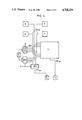
- FIG. 1 is a schematic circuit diagram of a first embodiment of the invention:
- FIG. 2 is a circuit diagram of a specific embodiment of an evaluation circuit AS
- FIG. 3 is a circuit diagram of a second embodiment of the invention.
- FIG. 4 is a circuit diagram of a third embodiment of the invention.
- FIG. 5 is a circuit diagram of the first embodiment of the invention applied to a memory with eight cell fields:
- FIG. 6 is a circuit diagram of the first embodiment of the invention, applied to a memory with data interfaces in a width of 2 bits:
- FIG. 7 is an illustration of two timing diagram
- FIG. 8 is a circuit diagram of another advantageous embodiment of an evaluation circuit AS.
- One of n data lines DL is connected to each cell field ZF. The data lines serve for writing information into the cell fields ZF and for reading the cell fields out.
- the addressing signal is connected to the most significant (A x ) of existing address terminals, from where it is written into the corresponding cell fields ZF.
- the data lines DL are connected to the data output terminal D o through a second data switch DW2.
- the second data switch DW2 is addressed address-wise exactly like the first data switch DW1.
- the second data switch DW2 connects one of the n data lines DL to the data output terminal D o .
- the parts of a semiconductor memory according to the invention described so far are already known by themselves. Such parts are applied, for instance, in semiconductor memories which permit the so-called "nibble mode" of operation.
- the gates of the transistors of the third data switch DW3 are addressed by a control signal P, the generation of which will be described below. If information is written through the third data switch DW3 into the cell fields ZF, all of the cell fields ZF contain the same information.
- test signal P which activates the third data switch DW3
- a test signal in the form of a constant potential is applied to a further terminal portion TA in the test case.
- a constant potential such as with the value "0" is applied, or the terminal TA remains unoccupied.
- the control signal P which is generated in this manner and which can be taken off directly at the terminal TA, then controls the gates of the transistors of the third data switch DW3 among other things so that the transistors are connected through.
- this structure has the advantage of permitting the selection of a potential value which is otherwise also used for addressing the semiconductor memory (for instance, "TTL level").
- TTL level a potential value which is otherwise also used for addressing the semiconductor memory
- an additional terminal is needed for the terminal TA which may not be available in some circumstances due to the dimensions of the housing of the semiconductor memory.
- a terminal which is otherwise used for normal operation is used concurrently.
- the most suitable terminal which is available is one which serves for addressing the semiconductor memory with address information, especially for the most significant X or Y or X/Y information (with the address multiplex method customary today).
- a (most significant) address signal A with a "0" level of 0 volts and a "1" level of 5 volts is applied to such a terminal in semiconductor memories which are customary today.
- this terminal is generally designated with reference symbol A x .
- the most significant X/Y address information is connected to the terminal A x .
- Discriminator circuit DS recognizes this applied potential and generates the control signal P internal to the semiconductor memory.
- Discriminator circuits DS are known in the art, such as in the form of threshold switches. Threshold switches can be found, for instance, in German Published, Non-Prosecuted Applications DE-OS No. 30 30 852 and DE-OS No. 33 18 564, the former corresponding to U.S. Pat. No. 4,458,338.
- Threshold switches can be found, for instance, in German Published, Non-Prosecuted Applications DE-OS No. 30 30 852 and DE-OS No. 33 18 564, the former corresponding to U.S. Pat. No. 4,458,338.
- other embodiments according to the state of the art are also conceivable.
- each of the evaluation circuits AS it is the purpose of each of the evaluation circuits AS to take over the information present on the n data lines DL assigned to the respective evaluation circuit AS when reading out from the semiconductor memory and to pass it on if all of this information is equal (which corresponds to the "o.k. case" due to the previously accomplished parallel storage into the cell fields ZF).
- the information is passed on through an output OUT Test to the data output terminal D o . If the data are not equal, the evaluation circuits AS bring the output OUT Test into a high-resistance state. In this way the output terminal D o also assumes a high-resistance state which is then recognized as an error by an automatic tester connected to the data output terminal D o .
- FIG. 2 A possible advantageous embodiment of the evaluation or selection circuit AS is shown in FIG. 2 and will be explained below.
- the first AND gate G1 switches at its output to a logical "1" only if all data lines DL are at logical "1". The same applies for the output of the second AND gate G2 (the output is a logical "1” only if all data lines DL are at logical "0").
- the evaluation circuit AS furthermore contains a first multivibrator circuit FF1, which may be in the form of an RS flip-flop with a setting input S, a resetting input R as well as an output Q.
- the setting input S is connected to the output of the first AND gate G1 and sets the output of the first multivibrator circuit FF1 to a logical "1", if a logical "1" is applied to all of the inputs of the first AND gate G1.
- the resetting input R is connected to the output of the second AND gate G2.
- the outputs of the two AND gates G1, G2 are connected in negated form to a third AND gate G3, parallel to the connection of the two inputs of the first multivibrator circuit FF1.
- the latter therefore acts likewise with a NOR function.
- the second multivibrator circuit FF2 also has a setting input S which is controlled by a setting circuit SS.
- the output of the first multivibrator circuit FF1 is connected to the source terminal of a transistor T.
- the output of the second multivibrator circuit FF2 is connected to the gate of the transistor T.
- the setting circuit SS is therefore reduced to supplying a machine clock frequency CLK. It is, of course, also possible to supply the machine clock frequency CLK of the setting circuit SS externally, such as through a module terminal from the automatic tester connected thereto.
- the output signal OUT Test assumes a higher resistance and consequently, the data output terminal D o also assumes a high-resistance state.
- FIG. 8 shows another advantageous embodiment of the evaluation circuit AS.
- the FIG. 8 device represents substantial simplifications of the circuitry.
- the FIG. 8 circuit contains only an OR gate OG.
- the source of the transistor T is connected directly to the output of the first AND gate G1.
- the output signal OUT Test is again generated at the drain of the transistor T.
- the gate of the transistor T is wired to the output of the OR gate OG.
- Each input of the OR gate OG is connected to an output of one of the two AND gates G1, G2.
- the embodiment of the invention according to FIG. 1 also includes a fourth data switch DW4 per bit of width m of the data interfaces, which, in normal operation serves for switching information OUT Norm leaving the respective second data switch DW2 to the respective data output terminal D o and which, during test operation serves for connecting the output signal OUT Test of the respective evaluation circuit AS to the respective data output terminal D o instead.
- This junction is provided by two transistors for each fourth data switch DW4.
- the source terminals of the transistors are connected together to the corresponding data output terminal D o .
- the drain terminal of one transistor is connected to the output of the second data switch DW2, while the drain terminal of the other transistor is connected to the output of the evaluation circuit AS.
- the gate of one transistor is addressed by a signal P which is complementary to the control signal P, while the gate of the other transistor is addressed by the control signal P. It is therefore possible to selectively switch the output of the second data switch DW2 or that of the evaluation circuit AS to the data output terminal D o . However, in another embodiment shown in FIG. 4, it is entirely possible to switch the output of each of the second data switches DW2 directly to the corresponding data output terminal D o and to similarly connect the output of each evaluation circuit AS directly and separately to a terminal PA of its own in the sense of a test terminal.
- the operation of the semiconductor memory is the same as described for FIG. 1. In test operation, an even greater reduction of the testing time is obtained.
- the operation is the same as described in FIG. 1. It must merely be clarified that both respective first data switches DW1, second data switches DW2, third data switches DW3, fourth data switches DW4, the cell fields ZF as well as the two evaluation circuits AS each operate in parallel with and independently of, each other.
Landscapes
- Tests Of Electronic Circuits (AREA)
- For Increasing The Reliability Of Semiconductor Memories (AREA)
- Test And Diagnosis Of Digital Computers (AREA)
- Heterocyclic Carbon Compounds Containing A Hetero Ring Having Oxygen Or Sulfur (AREA)
- Chemical And Physical Treatments For Wood And The Like (AREA)
- Polysaccharides And Polysaccharide Derivatives (AREA)
- Semiconductor Memories (AREA)
- Static Random-Access Memory (AREA)
- Techniques For Improving Reliability Of Storages (AREA)
Applications Claiming Priority (2)
| Application Number | Priority Date | Filing Date | Title |
|---|---|---|---|
| DE3532443 | 1985-09-11 | ||
| DE3532443 | 1985-09-11 |
Publications (1)
| Publication Number | Publication Date |
|---|---|
| US4768194A true US4768194A (en) | 1988-08-30 |
Family
ID=6280694
Family Applications (1)
| Application Number | Title | Priority Date | Filing Date |
|---|---|---|---|
| US06/906,454 Expired - Lifetime US4768194A (en) | 1985-09-11 | 1986-09-11 | Integrated semiconductor memory |
Country Status (7)
| Country | Link |
|---|---|
| US (1) | US4768194A (de) |
| EP (1) | EP0214508B1 (de) |
| JP (1) | JPS6262500A (de) |
| KR (1) | KR950014804B1 (de) |
| AT (1) | ATE67892T1 (de) |
| DE (1) | DE3681666D1 (de) |
| HK (1) | HK6793A (de) |
Cited By (7)
| Publication number | Priority date | Publication date | Assignee | Title |
|---|---|---|---|---|
| US4958324A (en) * | 1987-11-24 | 1990-09-18 | Sgs-Thomson Microelectronics Sa | Method for the testing of electrically programmable memory cells, and corresponding integrated circuit |
| US5075892A (en) * | 1988-12-31 | 1991-12-24 | Samsung Electronics Co. Ltd. | Parallel read circuit for testing high density memories |
| US5132937A (en) * | 1989-06-01 | 1992-07-21 | Mitsubishi Denki Kabushiki Kaisha | Semiconductor memory device having on-chip test circuit and operating method thereof |
| EP0600655A2 (de) * | 1992-11-23 | 1994-06-08 | Texas Instruments Incorporated | Verfahren und Vorrichtung zur Prüfung von zur integrierten Schaltung |
| US5661729A (en) * | 1995-04-28 | 1997-08-26 | Song Corporation | Semiconductor memory having built-in self-test circuit |
| US5809040A (en) * | 1995-09-28 | 1998-09-15 | Siemens Aktiengesellschaft | Testable circuit configuration having a plurality of identical circuit blocks |
| US5850509A (en) * | 1991-11-13 | 1998-12-15 | Intel Corporation | Circuitry for propagating test mode signals associated with a memory array |
Families Citing this family (2)
| Publication number | Priority date | Publication date | Assignee | Title |
|---|---|---|---|---|
| ATE65339T1 (de) * | 1984-12-28 | 1991-08-15 | Siemens Ag | Integrierter halbleiterspeicher. |
| JPS62170094A (ja) * | 1986-01-21 | 1987-07-27 | Mitsubishi Electric Corp | 半導体記憶回路 |
Citations (6)
| Publication number | Priority date | Publication date | Assignee | Title |
|---|---|---|---|---|
| US4458338A (en) * | 1980-08-14 | 1984-07-03 | Siemens Aktiengesellschaft | Circuit for checking memory cells of programmable MOS-integrated semiconductor memories |
| US4625162A (en) * | 1984-10-22 | 1986-11-25 | Monolithic Memories, Inc. | Fusible link short detector with array of reference fuses |
| US4625311A (en) * | 1984-06-18 | 1986-11-25 | Monolithic Memories, Inc. | Programmable array logic circuit with testing and verification circuitry |
| US4654827A (en) * | 1984-08-14 | 1987-03-31 | Texas Instruments Incorporated | High speed testing of semiconductor memory devices |
| US4686456A (en) * | 1985-06-18 | 1987-08-11 | Kabushiki Kaisha Toshiba | Memory test circuit |
| US4692923A (en) * | 1984-09-28 | 1987-09-08 | Ncr Corporation | Fault tolerant memory |
Family Cites Families (5)
| Publication number | Priority date | Publication date | Assignee | Title |
|---|---|---|---|---|
| JPS57105897A (en) * | 1980-12-23 | 1982-07-01 | Fujitsu Ltd | Semiconductor storage device |
| JPS58150198A (ja) * | 1982-03-03 | 1983-09-06 | Usac Electronics Ind Co Ltd | メモリのチエツク方式 |
| JPS59119597A (ja) * | 1982-12-27 | 1984-07-10 | Fujitsu Ltd | 半導体記憶装置 |
| DE3318564A1 (de) * | 1983-05-20 | 1984-11-22 | Siemens AG, 1000 Berlin und 8000 München | Integrierte digitale mos-halbleiterschaltung |
| JPS6015899A (ja) * | 1983-07-08 | 1985-01-26 | Hitachi Micro Comput Eng Ltd | 記憶装置 |
-
1986
- 1986-08-18 AT AT86111403T patent/ATE67892T1/de not_active IP Right Cessation
- 1986-08-18 DE DE8686111403T patent/DE3681666D1/de not_active Expired - Lifetime
- 1986-08-18 EP EP86111403A patent/EP0214508B1/de not_active Expired - Lifetime
- 1986-09-04 JP JP61209804A patent/JPS6262500A/ja active Pending
- 1986-09-09 KR KR1019860007527A patent/KR950014804B1/ko not_active IP Right Cessation
- 1986-09-11 US US06/906,454 patent/US4768194A/en not_active Expired - Lifetime
-
1993
- 1993-01-28 HK HK67/93A patent/HK6793A/xx not_active IP Right Cessation
Patent Citations (6)
| Publication number | Priority date | Publication date | Assignee | Title |
|---|---|---|---|---|
| US4458338A (en) * | 1980-08-14 | 1984-07-03 | Siemens Aktiengesellschaft | Circuit for checking memory cells of programmable MOS-integrated semiconductor memories |
| US4625311A (en) * | 1984-06-18 | 1986-11-25 | Monolithic Memories, Inc. | Programmable array logic circuit with testing and verification circuitry |
| US4654827A (en) * | 1984-08-14 | 1987-03-31 | Texas Instruments Incorporated | High speed testing of semiconductor memory devices |
| US4692923A (en) * | 1984-09-28 | 1987-09-08 | Ncr Corporation | Fault tolerant memory |
| US4625162A (en) * | 1984-10-22 | 1986-11-25 | Monolithic Memories, Inc. | Fusible link short detector with array of reference fuses |
| US4686456A (en) * | 1985-06-18 | 1987-08-11 | Kabushiki Kaisha Toshiba | Memory test circuit |
Non-Patent Citations (5)
| Title |
|---|
| Elektronik, No. 15, Jul. 30, 1982, pp. 27 to 30. * |
| IEEE International Solid State Circuit Conference, 1981, pp. 84 to 85. * |
| IEEE International Solid-State Circuit Conference, 1981, pp. 84 to 85. |
| Patents Abstract of Japan, vol. 6, (P 111) 940 , Apr. 21, 1982. * |
| Patents Abstract of Japan, vol. 6, (P-111)[940], Apr. 21, 1982. |
Cited By (8)
| Publication number | Priority date | Publication date | Assignee | Title |
|---|---|---|---|---|
| US4958324A (en) * | 1987-11-24 | 1990-09-18 | Sgs-Thomson Microelectronics Sa | Method for the testing of electrically programmable memory cells, and corresponding integrated circuit |
| US5075892A (en) * | 1988-12-31 | 1991-12-24 | Samsung Electronics Co. Ltd. | Parallel read circuit for testing high density memories |
| US5132937A (en) * | 1989-06-01 | 1992-07-21 | Mitsubishi Denki Kabushiki Kaisha | Semiconductor memory device having on-chip test circuit and operating method thereof |
| US5850509A (en) * | 1991-11-13 | 1998-12-15 | Intel Corporation | Circuitry for propagating test mode signals associated with a memory array |
| EP0600655A2 (de) * | 1992-11-23 | 1994-06-08 | Texas Instruments Incorporated | Verfahren und Vorrichtung zur Prüfung von zur integrierten Schaltung |
| EP0600655A3 (de) * | 1992-11-23 | 1996-12-11 | Texas Instruments Inc | Verfahren und Vorrichtung zur Prüfung von zur integrierten Schaltung. |
| US5661729A (en) * | 1995-04-28 | 1997-08-26 | Song Corporation | Semiconductor memory having built-in self-test circuit |
| US5809040A (en) * | 1995-09-28 | 1998-09-15 | Siemens Aktiengesellschaft | Testable circuit configuration having a plurality of identical circuit blocks |
Also Published As
| Publication number | Publication date |
|---|---|
| HK6793A (en) | 1993-02-05 |
| DE3681666D1 (de) | 1991-10-31 |
| JPS6262500A (ja) | 1987-03-19 |
| EP0214508A2 (de) | 1987-03-18 |
| EP0214508B1 (de) | 1991-09-25 |
| ATE67892T1 (de) | 1991-10-15 |
| EP0214508A3 (en) | 1989-05-03 |
| KR870003505A (ko) | 1987-04-17 |
| KR950014804B1 (ko) | 1995-12-14 |
Similar Documents
| Publication | Publication Date | Title |
|---|---|---|
| US4752929A (en) | Method of operating a semiconductor memory with a capability of testing, and an evaluation circuit for performing the method | |
| US4418403A (en) | Semiconductor memory cell margin test circuit | |
| KR910000738B1 (ko) | 동작 테스트실행에 적합한 반도체 집적회로 | |
| KR900004886B1 (ko) | 메모리 테스트회로 | |
| US4495603A (en) | Test system for segmented memory | |
| US5005158A (en) | Redundancy for serial memory | |
| US4956819A (en) | Circuit configuration and a method of testing storage cells | |
| US5436911A (en) | Semiconductor memory device comprising a test circuit and a method of operation thereof | |
| US4862416A (en) | Semiconductor memory device with redundant memory cell | |
| EP0205258B1 (de) | Integrierte Halbleiterschaltung mit einer Schaltfunktion der Betriebsarten einer internen Schaltung | |
| KR0160325B1 (ko) | 비트 단위 데이타의 입력 및 출력용 반도체 메모리 장치 | |
| US4768194A (en) | Integrated semiconductor memory | |
| US4742490A (en) | Integrated semiconductor memory | |
| US4320507A (en) | Field programmable device having test provisions for fault detection | |
| US4742489A (en) | Integrated semiconductor memory | |
| KR900008191B1 (ko) | 대치 용장회로를 가진 반도체집적회로 | |
| US4586170A (en) | Semiconductor memory redundant element identification circuit | |
| US5825712A (en) | Semiconductor integrated circuit | |
| US4581739A (en) | Electronically selectable redundant array (ESRA) | |
| US6301678B1 (en) | Test circuit for reducing test time in semiconductor memory device having multiple data input/output terminals | |
| EP0520696B1 (de) | Integrierte Halbleiterspeicherschaltung mit einem Diskriminator für eine diagnostische Betriebsart | |
| US6519726B1 (en) | Semiconductor device and testing method of the same | |
| KR940011428B1 (ko) | 반도체 기억장치의 테스트 회로 | |
| US5815001A (en) | Integrated circuit board with built-in terminal connection testing circuitry | |
| JPH07312100A (ja) | 半導体メモリ集積回路 |
Legal Events
| Date | Code | Title | Description |
|---|---|---|---|
| AS | Assignment |
Owner name: SIEMENS AKTIENGESELLSCHAFT, BERLIN AND MUENCHEN, G Free format text: ASSIGNMENT OF ASSIGNORS INTEREST.;ASSIGNOR:FUCHS, HANS P.;REEL/FRAME:004901/0061 Effective date: 19860826 Owner name: SIEMENS AKTIENGESELLSCHAFT, A GERMAN CORP.,GERMANY Free format text: ASSIGNMENT OF ASSIGNORS INTEREST;ASSIGNOR:FUCHS, HANS P.;REEL/FRAME:004901/0061 Effective date: 19860826 |
|
| STCF | Information on status: patent grant |
Free format text: PATENTED CASE |
|
| FEPP | Fee payment procedure |
Free format text: PAYOR NUMBER ASSIGNED (ORIGINAL EVENT CODE: ASPN); ENTITY STATUS OF PATENT OWNER: LARGE ENTITY |
|
| FPAY | Fee payment |
Year of fee payment: 4 |
|
| FPAY | Fee payment |
Year of fee payment: 8 |
|
| FPAY | Fee payment |
Year of fee payment: 12 |
|
| AS | Assignment |
Owner name: INFINEON TECHNOLOGIES AG, GERMANY Free format text: ASSIGNMENT OF ASSIGNORS INTEREST;ASSIGNOR:SIEMENS AKTIENGESELLSCHAFT;REEL/FRAME:014815/0743 Effective date: 20040625 |