US4729962A - Semiconductor junction formation by directed heat - Google Patents
Semiconductor junction formation by directed heat Download PDFInfo
- Publication number
- US4729962A US4729962A US06/843,486 US84348686A US4729962A US 4729962 A US4729962 A US 4729962A US 84348686 A US84348686 A US 84348686A US 4729962 A US4729962 A US 4729962A
- Authority
- US
- United States
- Prior art keywords
- web
- type
- high intensity
- dopant
- face
- Prior art date
- Legal status (The legal status is an assumption and is not a legal conclusion. Google has not performed a legal analysis and makes no representation as to the accuracy of the status listed.)
- Expired - Fee Related
Links
Images
Classifications
-
- H—ELECTRICITY
- H01—ELECTRIC ELEMENTS
- H01L—SEMICONDUCTOR DEVICES NOT COVERED BY CLASS H10
- H01L21/00—Processes or apparatus adapted for the manufacture or treatment of semiconductor or solid state devices or of parts thereof
- H01L21/02—Manufacture or treatment of semiconductor devices or of parts thereof
- H01L21/04—Manufacture or treatment of semiconductor devices or of parts thereof the devices having at least one potential-jump barrier or surface barrier, e.g. PN junction, depletion layer or carrier concentration layer
- H01L21/18—Manufacture or treatment of semiconductor devices or of parts thereof the devices having at least one potential-jump barrier or surface barrier, e.g. PN junction, depletion layer or carrier concentration layer the devices having semiconductor bodies comprising elements of Group IV of the Periodic System or AIIIBV compounds with or without impurities, e.g. doping materials
- H01L21/26—Bombardment with radiation
- H01L21/263—Bombardment with radiation with high-energy radiation
- H01L21/268—Bombardment with radiation with high-energy radiation using electromagnetic radiation, e.g. laser radiation
-
- H—ELECTRICITY
- H01—ELECTRIC ELEMENTS
- H01L—SEMICONDUCTOR DEVICES NOT COVERED BY CLASS H10
- H01L21/00—Processes or apparatus adapted for the manufacture or treatment of semiconductor or solid state devices or of parts thereof
- H01L21/02—Manufacture or treatment of semiconductor devices or of parts thereof
- H01L21/04—Manufacture or treatment of semiconductor devices or of parts thereof the devices having at least one potential-jump barrier or surface barrier, e.g. PN junction, depletion layer or carrier concentration layer
- H01L21/18—Manufacture or treatment of semiconductor devices or of parts thereof the devices having at least one potential-jump barrier or surface barrier, e.g. PN junction, depletion layer or carrier concentration layer the devices having semiconductor bodies comprising elements of Group IV of the Periodic System or AIIIBV compounds with or without impurities, e.g. doping materials
- H01L21/22—Diffusion of impurity materials, e.g. doping materials, electrode materials, into or out of a semiconductor body, or between semiconductor regions; Interactions between two or more impurities; Redistribution of impurities
- H01L21/225—Diffusion of impurity materials, e.g. doping materials, electrode materials, into or out of a semiconductor body, or between semiconductor regions; Interactions between two or more impurities; Redistribution of impurities using diffusion into or out of a solid from or into a solid phase, e.g. a doped oxide layer
- H01L21/2251—Diffusion into or out of group IV semiconductors
- H01L21/2254—Diffusion into or out of group IV semiconductors from or through or into an applied layer, e.g. photoresist, nitrides
-
- Y—GENERAL TAGGING OF NEW TECHNOLOGICAL DEVELOPMENTS; GENERAL TAGGING OF CROSS-SECTIONAL TECHNOLOGIES SPANNING OVER SEVERAL SECTIONS OF THE IPC; TECHNICAL SUBJECTS COVERED BY FORMER USPC CROSS-REFERENCE ART COLLECTIONS [XRACs] AND DIGESTS
- Y10—TECHNICAL SUBJECTS COVERED BY FORMER USPC
- Y10S—TECHNICAL SUBJECTS COVERED BY FORMER USPC CROSS-REFERENCE ART COLLECTIONS [XRACs] AND DIGESTS
- Y10S148/00—Metal treatment
- Y10S148/014—Capacitor
-
- Y—GENERAL TAGGING OF NEW TECHNOLOGICAL DEVELOPMENTS; GENERAL TAGGING OF CROSS-SECTIONAL TECHNOLOGIES SPANNING OVER SEVERAL SECTIONS OF THE IPC; TECHNICAL SUBJECTS COVERED BY FORMER USPC CROSS-REFERENCE ART COLLECTIONS [XRACs] AND DIGESTS
- Y10—TECHNICAL SUBJECTS COVERED BY FORMER USPC
- Y10S—TECHNICAL SUBJECTS COVERED BY FORMER USPC CROSS-REFERENCE ART COLLECTIONS [XRACs] AND DIGESTS
- Y10S148/00—Metal treatment
- Y10S148/093—Laser beam treatment in general
Definitions
- This invention pertains to the art of semiconductor junction formation.
- junctions in silicon webs such as dendritic silicon webs for use as photovoltaic solar cells, for example, is typically carried out in a tube-type or belt-type diffusion furnace. If junctions are to be formed in both faces of the web, a two-step process is required in which a dopant layer is first diffused into one face, the face is then cleaned and masked as with silicon dioxide, SiO 2 , to prevent cross-over of dopant from the diffused layer to the to-be-diffused layer at the opposite face and then, in a separate operation, another dopant layer is diffused into the opposite face.
- the heat-up to, say, 850°-950° C. and the subsequent cool-down for each separate layer may typically take 40 minutes or so.
- An important aspect of the invention is that the heat required to diffuse in the dopants is supplied by a relatively short duration pulse of high intensity light.
- the method according to the invention for forming one or more semiconductor junctions in a silicon web of a given P- or N-type includes applying a liquid precursor containing a dopant of a desired P- or N-type to at least one face of the web, baking the web sufficiently to remove excess solvent, and then heating the web rapidly with a pulsed high intensity light for a period of less than a minute at temperatures in a range from about 950° C. to 1200° C.
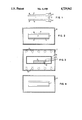
- FIG. 1 is a simplified edge view of a web to which liquid precursors containing dopants is being applied to opposite faces of the web;
- FIG. 2 is a simplified view of the web of FIG. 1 in an oven for baking;
- FIG. 3 is a simplified face view of the doped web located in a pulse high intensity light device for undergoing the rapid heating step
- FIG. 4 is a simplified view of the web of FIG. 3 in an annealing oven.
- a predoped, P-type, dendritic silicon web 2 has a liquid precursor 4 containing an N-type dopant to one face of the web 2 and a liquid precursor 6 containing a P-type dopant is applied to the opposite face of the web 2.
- the liquid precursors may be applied in conventional fashion such as by using a foam brush 8, a meniscus coater or by a chemical vapor deposition method. Examples of the precursors which may be used are those which are commercially available, such as Allied Chemical Corp. P8 or Filmtronics, Inc. P2.5 for the precursor of the N-type, and Allied Chemical Corp. B150 for the P-type.
- the web 2 with the applied precursors 4 and 6 is then baked in an oven 10 (FIG. 2) to remove the excess solvent from the faces of the web.
- the oven 10 may be an air environment oven which is heated to approximately 200° C. and the web is heated at that temperature for, say, 20 minutes or so to remove the excess solvent.
- the next step in the process is the rapid heating of the doped web by a pulsed high intensity light in a mechanism 12 as schematically shown in FIG. 3.
- the rapid thermal heater 12 of FIG. 3 is a tungsten halogen system such as is commercially available, for example, from A. G. Associates of Palo Alto, Calif. As publicly disclosed by this entity, the tungsten halogen system uses banks of tungsten halogen lamps 14 positioned above and below the web which, in the A. G. Associates' heat pulsed mechanism is placed in a quartz tube 16 for promoting thermal efficiency.
- the web 2 is heated inside the mechanism 12 by pulsed high intensity light from the tungsten halogen lamps for a period of less than a minute at temperatures in a range from about 1000° C. to 1150° C. to simultaneously form junctions in both faces of the web.
- the preferred temperature and time for forming simultaneous junctions in both faces of the dendritic silicon web for use in solar cells is 950° C. to 1200° C. for about 5-15 seconds. This produces relatively shallow junctions which are preferable for solar cells. To obtain deeper junctions for other devices such as rectifiers and transistors, etc., the time and temperature may be increased proportionately.
- thermocouple 18 may be embedded in web material 20 thermally similar to the web 20, as suggested by A. G. Associates. It will be apparent that other temperature measurement and control system may also be used in carrying out the invention.
- the doping which takes place in the rapid thermal processing occurs more quickly than a period of time which would permit cross-over of the dopant from one face of the web to the other face of the web and thereby permit contamination.
- the inventive process only a single step is required in the doping so that the complicated and expensive two-step process of the conventional prior art is avoided, along with the cleaning and masking.
- the annealing is known to be able to take out defects in the web which are frozen in during too rapid cooling of the web.
- the annealing is done to provide for higher efficiencies for solar cells and to provide for higher carrier lifetimes for other semiconductors.
- the annealing may take place in an air environment oven 22 of FIG. 4 and in which the web 2 is heated in air at 750° C. to 850° C. for anywhere from 10 to 60 minutes.
Landscapes
- Physics & Mathematics (AREA)
- Engineering & Computer Science (AREA)
- High Energy & Nuclear Physics (AREA)
- Condensed Matter Physics & Semiconductors (AREA)
- General Physics & Mathematics (AREA)
- Manufacturing & Machinery (AREA)
- Computer Hardware Design (AREA)
- Microelectronics & Electronic Packaging (AREA)
- Power Engineering (AREA)
- Optics & Photonics (AREA)
- Health & Medical Sciences (AREA)
- Toxicology (AREA)
- Electromagnetism (AREA)
- Photovoltaic Devices (AREA)
Priority Applications (5)
| Application Number | Priority Date | Filing Date | Title |
|---|---|---|---|
| US06/843,486 US4729962A (en) | 1986-03-24 | 1986-03-24 | Semiconductor junction formation by directed heat |
| FR8616556A FR2596201A1 (fr) | 1986-03-24 | 1986-11-27 | Procede de fabrication de jonctions semi-conductrices et produits ainsi obtenus |
| GB8628541A GB2188481B (en) | 1986-03-24 | 1986-11-28 | Method of forming semiconductor junctions |
| DE19863640713 DE3640713A1 (de) | 1986-03-24 | 1986-11-28 | Verfahren zur bildung von halbleiteruebergaengen |
| JP61316136A JP2610853B2 (ja) | 1986-03-24 | 1986-12-26 | 半導体の接合形成方法 |
Applications Claiming Priority (1)
| Application Number | Priority Date | Filing Date | Title |
|---|---|---|---|
| US06/843,486 US4729962A (en) | 1986-03-24 | 1986-03-24 | Semiconductor junction formation by directed heat |
Publications (1)
| Publication Number | Publication Date |
|---|---|
| US4729962A true US4729962A (en) | 1988-03-08 |
Family
ID=25290132
Family Applications (1)
| Application Number | Title | Priority Date | Filing Date |
|---|---|---|---|
| US06/843,486 Expired - Fee Related US4729962A (en) | 1986-03-24 | 1986-03-24 | Semiconductor junction formation by directed heat |
Country Status (5)
| Country | Link |
|---|---|
| US (1) | US4729962A (fr) |
| JP (1) | JP2610853B2 (fr) |
| DE (1) | DE3640713A1 (fr) |
| FR (1) | FR2596201A1 (fr) |
| GB (1) | GB2188481B (fr) |
Cited By (6)
| Publication number | Priority date | Publication date | Assignee | Title |
|---|---|---|---|---|
| US5278097A (en) * | 1989-07-31 | 1994-01-11 | Texas Instruments Incorporated | Method of making doped silicon spheres |
| US5395794A (en) * | 1993-04-22 | 1995-03-07 | Sklyarevich; Vladislav E. | Method of treating semiconductor materials |
| US5399523A (en) * | 1991-03-26 | 1995-03-21 | Siemens Aktiengesellscaft | Method for the rapid thermal processing of a semiconductor wafer by irradiation |
| WO1996008043A1 (fr) * | 1994-09-09 | 1996-03-14 | Georgia Tech Research Corporation | Procedes pour produire a bas prix des cellules solaires en silicium a grand rendement |
| US5527389A (en) * | 1992-08-07 | 1996-06-18 | Ase Americas, Inc. | Apparatus for forming diffusion junctions in solar cell substrates |
| US6143633A (en) * | 1995-10-05 | 2000-11-07 | Ebara Solar, Inc. | In-situ diffusion of dopant impurities during dendritic web growth of crystal ribbon |
Families Citing this family (2)
| Publication number | Priority date | Publication date | Assignee | Title |
|---|---|---|---|---|
| DE4331937A1 (de) * | 1993-09-16 | 1994-03-17 | Ulrich Prof Dr Mohr | Verfahren zur Eindiffusion von Dotanten in Halbleiterfestkörper |
| US20180025912A1 (en) * | 2015-02-25 | 2018-01-25 | Toray Industries, Inc. | P-type impurity-diffusing composition, method for manufacturing semiconductor device using said composition, solar cell, and method for manufacturing said solar cell |
Citations (9)
| Publication number | Priority date | Publication date | Assignee | Title |
|---|---|---|---|---|
| US3940289A (en) * | 1975-02-03 | 1976-02-24 | The United States Of America As Represented By The Secretary Of The Navy | Flash melting method for producing new impurity distributions in solids |
| US4273950A (en) * | 1979-05-29 | 1981-06-16 | Photowatt International, Inc. | Solar cell and fabrication thereof using microwaves |
| JPS5948402A (ja) * | 1982-09-14 | 1984-03-19 | Asahi Chem Ind Co Ltd | 携帯用殺虫マツト |
| US4443493A (en) * | 1980-04-28 | 1984-04-17 | Fairchild Camera And Instrument Corp. | Laser induced flow glass materials |
| US4482393A (en) * | 1979-12-17 | 1984-11-13 | Sony Corporation | Method of activating implanted ions by incoherent light beam |
| US4514440A (en) * | 1983-12-12 | 1985-04-30 | Allied Corporation | Spin-on dopant method |
| US4539431A (en) * | 1983-06-06 | 1985-09-03 | Sera Solar Corporation | Pulse anneal method for solar cell |
| US4619036A (en) * | 1984-09-28 | 1986-10-28 | Texas Instruments Incorporated | Self-aligned low-temperature emitter drive-in |
| US4621411A (en) * | 1984-09-28 | 1986-11-11 | Texas Instruments Incorporated | Laser-enhanced drive in of source and drain diffusions |
Family Cites Families (9)
| Publication number | Priority date | Publication date | Assignee | Title |
|---|---|---|---|---|
| JPS5552221A (en) * | 1978-10-12 | 1980-04-16 | Toshiba Corp | Impurity dispersion method and its device |
| JPS55127016A (en) * | 1979-03-26 | 1980-10-01 | Hitachi Ltd | Manufacturing of semiconductor device |
| FR2507822A1 (fr) * | 1979-05-29 | 1982-12-17 | Photowatt International | Procede de fabrication de cellules solaires et cellules solaires correspondantes |
| CA1177148A (fr) * | 1981-10-06 | 1984-10-30 | Robert J. Mcintyre | Reseau de photodiodes a avalanche |
| US4571366A (en) * | 1982-02-11 | 1986-02-18 | Owens-Illinois, Inc. | Process for forming a doped oxide film and doped semiconductor |
| JPS58186933A (ja) * | 1982-04-23 | 1983-11-01 | Sharp Corp | 半導体素子の製造方法 |
| JPS58223320A (ja) * | 1982-06-22 | 1983-12-24 | Ushio Inc | 不純物拡散方法 |
| DE3340874A1 (de) * | 1983-11-11 | 1985-05-23 | Telefunken electronic GmbH, 7100 Heilbronn | Verfahren zum herstellen einer solarzelle |
| US4521441A (en) * | 1983-12-19 | 1985-06-04 | Motorola, Inc. | Plasma enhanced diffusion process |
-
1986
- 1986-03-24 US US06/843,486 patent/US4729962A/en not_active Expired - Fee Related
- 1986-11-27 FR FR8616556A patent/FR2596201A1/fr active Pending
- 1986-11-28 GB GB8628541A patent/GB2188481B/en not_active Expired
- 1986-11-28 DE DE19863640713 patent/DE3640713A1/de not_active Ceased
- 1986-12-26 JP JP61316136A patent/JP2610853B2/ja not_active Expired - Lifetime
Patent Citations (9)
| Publication number | Priority date | Publication date | Assignee | Title |
|---|---|---|---|---|
| US3940289A (en) * | 1975-02-03 | 1976-02-24 | The United States Of America As Represented By The Secretary Of The Navy | Flash melting method for producing new impurity distributions in solids |
| US4273950A (en) * | 1979-05-29 | 1981-06-16 | Photowatt International, Inc. | Solar cell and fabrication thereof using microwaves |
| US4482393A (en) * | 1979-12-17 | 1984-11-13 | Sony Corporation | Method of activating implanted ions by incoherent light beam |
| US4443493A (en) * | 1980-04-28 | 1984-04-17 | Fairchild Camera And Instrument Corp. | Laser induced flow glass materials |
| JPS5948402A (ja) * | 1982-09-14 | 1984-03-19 | Asahi Chem Ind Co Ltd | 携帯用殺虫マツト |
| US4539431A (en) * | 1983-06-06 | 1985-09-03 | Sera Solar Corporation | Pulse anneal method for solar cell |
| US4514440A (en) * | 1983-12-12 | 1985-04-30 | Allied Corporation | Spin-on dopant method |
| US4619036A (en) * | 1984-09-28 | 1986-10-28 | Texas Instruments Incorporated | Self-aligned low-temperature emitter drive-in |
| US4621411A (en) * | 1984-09-28 | 1986-11-11 | Texas Instruments Incorporated | Laser-enhanced drive in of source and drain diffusions |
Non-Patent Citations (3)
| Title |
|---|
| Kato et al., Jour. Electrochem. Soc. (Jul. 1985), p. 1730. * |
| Sedwick, Jour. Electrochem. Soc. 130 (1983), 484. * |
| USAMI et al., 18th Photovoltiaic . . . Conf., Las Vegas, Nevada, Oct. 1985. * |
Cited By (7)
| Publication number | Priority date | Publication date | Assignee | Title |
|---|---|---|---|---|
| US5278097A (en) * | 1989-07-31 | 1994-01-11 | Texas Instruments Incorporated | Method of making doped silicon spheres |
| US5399523A (en) * | 1991-03-26 | 1995-03-21 | Siemens Aktiengesellscaft | Method for the rapid thermal processing of a semiconductor wafer by irradiation |
| US5527389A (en) * | 1992-08-07 | 1996-06-18 | Ase Americas, Inc. | Apparatus for forming diffusion junctions in solar cell substrates |
| US5395794A (en) * | 1993-04-22 | 1995-03-07 | Sklyarevich; Vladislav E. | Method of treating semiconductor materials |
| WO1996008043A1 (fr) * | 1994-09-09 | 1996-03-14 | Georgia Tech Research Corporation | Procedes pour produire a bas prix des cellules solaires en silicium a grand rendement |
| US5510271A (en) * | 1994-09-09 | 1996-04-23 | Georgia Tech Research Corporation | Processes for producing low cost, high efficiency silicon solar cells |
| US6143633A (en) * | 1995-10-05 | 2000-11-07 | Ebara Solar, Inc. | In-situ diffusion of dopant impurities during dendritic web growth of crystal ribbon |
Also Published As
| Publication number | Publication date |
|---|---|
| JPS62226671A (ja) | 1987-10-05 |
| JP2610853B2 (ja) | 1997-05-14 |
| DE3640713A1 (de) | 1987-10-08 |
| GB2188481B (en) | 1989-12-20 |
| GB8628541D0 (en) | 1987-01-07 |
| FR2596201A1 (fr) | 1987-09-25 |
| GB2188481A (en) | 1987-09-30 |
Similar Documents
| Publication | Publication Date | Title |
|---|---|---|
| US4482393A (en) | Method of activating implanted ions by incoherent light beam | |
| US4041278A (en) | Heating apparatus for temperature gradient zone melting | |
| KR101078708B1 (ko) | 가열원들의 조합제들을 이용한 펄스 처리 반도체 가열방법들 | |
| Fulks et al. | Rapid isothermal annealing of ion implantation damage using a thermal radiation source | |
| US4001047A (en) | Temperature gradient zone melting utilizing infrared radiation | |
| US4661177A (en) | Method for doping semiconductor wafers by rapid thermal processing of solid planar diffusion sources | |
| US20020017311A1 (en) | Apparatus and method for rapid photo-thermal surface treatment | |
| JPS6411712B2 (fr) | ||
| US4729962A (en) | Semiconductor junction formation by directed heat | |
| EP1886339A4 (fr) | Procede et appareil permettant l'hydrogenaton d'un film mince de silicium sur du verre | |
| JPH0263293B2 (fr) | ||
| US4514440A (en) | Spin-on dopant method | |
| JPH0377657B2 (fr) | ||
| JPS59211221A (ja) | イオン注入した半導体の熱処理方法 | |
| Wilson et al. | Fast diffusion of As in polycrystalline silicon during rapid thermal annealing | |
| Borisenko et al. | Incoherent light annealing of phosphorus‐doped polycrystalline silicon | |
| JPH06508957A (ja) | 固体ドーパントソースと急速熱処理を使用してシリコンウェーハをドープする方法と装置 | |
| Komatsu et al. | Infrared radiation annealing for extended‐defect reduction in As‐implanted Si crystals | |
| Bentini | Solid state annealing of ion implanted silicon by incoherent light pulses and multiscan electron beam | |
| Gelpey et al. | Rapid annealing using the water-wall arc lamp | |
| JPH0198223A (ja) | シリコンウェーハの不純物拡散方法 | |
| JPH07142754A (ja) | 多結晶シリコン素子の製造方法 | |
| Hammond et al. | Design and fabrication of a high-damage threshold infrared Smartt interferometer | |
| Campbell | Flat-plate solar array project process development area: Process research of non-CZ silicon material | |
| Mercier et al. | Rapid Isothermal Fusion of BPSG Films |
Legal Events
| Date | Code | Title | Description |
|---|---|---|---|
| AS | Assignment |
Owner name: WESTINGHOUSE ELECTRIC CORPORATION, WESTINGHOUSE BU Free format text: ASSIGNMENT OF ASSIGNORS INTEREST.;ASSIGNOR:CAMPBELL, ROBERT B.;REEL/FRAME:004531/0472 Effective date: 19860310 |
|
| AS | Assignment |
Owner name: UNITED STATES OF AMERICA, AS REPRESENTED BY THE DE Free format text: ASSIGNMENT OF ASSIGNORS INTEREST. SUBJECT TO LICENSE RECITED;ASSIGNOR:WESTINGHOUSE ELECTRIC CORPORATION;REEL/FRAME:004705/0495 Effective date: 19870225 Owner name: UNITED STATES OF AMERICA, AS REPRESENTED BY THE DE Free format text: ASSIGNMENT OF ASSIGNORS INTEREST;ASSIGNOR:WESTINGHOUSE ELECTRIC CORPORATION;REEL/FRAME:004705/0495 Effective date: 19870225 |
|
| FPAY | Fee payment |
Year of fee payment: 4 |
|
| FEPP | Fee payment procedure |
Free format text: PAYER NUMBER DE-ASSIGNED (ORIGINAL EVENT CODE: RMPN); ENTITY STATUS OF PATENT OWNER: LARGE ENTITY Free format text: PAYOR NUMBER ASSIGNED (ORIGINAL EVENT CODE: ASPN); ENTITY STATUS OF PATENT OWNER: LARGE ENTITY |
|
| FPAY | Fee payment |
Year of fee payment: 8 |
|
| REMI | Maintenance fee reminder mailed | ||
| LAPS | Lapse for failure to pay maintenance fees | ||
| FP | Lapsed due to failure to pay maintenance fee |
Effective date: 20000308 |
|
| STCH | Information on status: patent discontinuation |
Free format text: PATENT EXPIRED DUE TO NONPAYMENT OF MAINTENANCE FEES UNDER 37 CFR 1.362 |