US4684801A - Signal preconditioning for touch entry device - Google Patents
Signal preconditioning for touch entry device Download PDFInfo
- Publication number
- US4684801A US4684801A US06/835,015 US83501586A US4684801A US 4684801 A US4684801 A US 4684801A US 83501586 A US83501586 A US 83501586A US 4684801 A US4684801 A US 4684801A
- Authority
- US
- United States
- Prior art keywords
- digital
- analog
- signal
- light
- array
- Prior art date
- Legal status (The legal status is an assumption and is not a legal conclusion. Google has not performed a legal analysis and makes no representation as to the accuracy of the status listed.)
- Expired - Fee Related
Links
Images


Classifications
-
- G—PHYSICS
- G06—COMPUTING OR CALCULATING; COUNTING
- G06F—ELECTRIC DIGITAL DATA PROCESSING
- G06F3/00—Input arrangements for transferring data to be processed into a form capable of being handled by the computer; Output arrangements for transferring data from processing unit to output unit, e.g. interface arrangements
- G06F3/01—Input arrangements or combined input and output arrangements for interaction between user and computer
- G06F3/03—Arrangements for converting the position or the displacement of a member into a coded form
- G06F3/041—Digitisers, e.g. for touch screens or touch pads, characterised by the transducing means
- G06F3/042—Digitisers, e.g. for touch screens or touch pads, characterised by the transducing means by opto-electronic means
- G06F3/0421—Digitisers, e.g. for touch screens or touch pads, characterised by the transducing means by opto-electronic means by interrupting or reflecting a light beam, e.g. optical touch-screen
-
- G—PHYSICS
- G01—MEASURING; TESTING
- G01V—GEOPHYSICS; GRAVITATIONAL MEASUREMENTS; DETECTING MASSES OR OBJECTS; TAGS
- G01V8/00—Prospecting or detecting by optical means
- G01V8/10—Detecting, e.g. by using light barriers
- G01V8/20—Detecting, e.g. by using light barriers using multiple transmitters or receivers
-
- H—ELECTRICITY
- H03—ELECTRONIC CIRCUITRY
- H03K—PULSE TECHNIQUE
- H03K17/00—Electronic switching or gating, i.e. not by contact-making and –breaking
- H03K17/94—Electronic switching or gating, i.e. not by contact-making and –breaking characterised by the way in which the control signals are generated
- H03K17/941—Electronic switching or gating, i.e. not by contact-making and –breaking characterised by the way in which the control signals are generated using an optical detector
Definitions
- Detection systems comprising a plurality of light emitting and detecting pairs located around the periphery of an irradiated field have been employed in a number of applications.
- infrared detector fields can be used as a safety interlock or an anti-intrusion system for preventing access to a certain area or as a safety barrier around a machine.
- One ever increasing use of such systems is as a touch input device to an electronic display.
- an array of infrared light emitters and detectors can be positioned around the periphery of an electronic display such as a CRT or a flat panel display.
- a number of such systems employ an X-Y matrix of emitters and detectors with associated emitters and detectors being axially aligned in pairs.
- a touch input system would be characterized as a far-looking application. Near-looking applications are those applications in which the emitter and detector are located in close proximity. The majority of the applications for conventional infrared opto devices emitters and detectors employ a separation of only a few centimeters. Many touch input systems position the emitters and detectors more than a foot apart, and some have a spacing of several feet. In near looking applications in which the opto devices are closely spaced, the total power output of the devices is more critical than the on-axis intensity.
- LEDs produced in the same process may range in light output by a factor of up to 4 to 1.
- Conventional phototransistors may range in sensitivity by the same factor. Therefore, when randomly paired together to form emitter/detector pairs, the output signals can vary over a range of 16 to 1 or even greater. This wide range of output signal can create difficulties in processing the output signals to determine broken beams.
- Careful preselection of available opto devices is one method of obtaining acceptable performance for touch input systems. Many of the opto devices from any manufacturing batch must be excluded as totally unacceptable for use in touch input systems. Thus, devices at the low end of the distribution must be totally eliminated. This preselection is based on total power output rather than on-axis intensity so that even the "better" opto devices may not be suitable for use in touch input systems. Thus, devices which may pass a selection process based on total power output may fail when the alignment problems associated with mounting the devices are combined with low on-axis intensity. Random pairing of devices will result in some devices producing below minimum output signals. Generally, the opto devices in a touch input matrix are mounted on printed circuit boards, and the complete assembly is tested.
- touch input systems employing signal preconditioning in the manner described herein can be used to compensate for environmental contaminates such as dirt or dust which reduce the output signal of opto pairs.
- Signal preconditioning also allows for special treatment at the edges of an opto matrix device, where reflection has traditionally been a problem.
- Signal preconditioning also permits a reduction in the LED drive current, allowing the selection of low current and lower cost multiplexing devices. In addition, lower LED drive current will extend the life of the LEDs. Low drive current also reduces the effect of thermal shock on LEDs.
- Signal preconditioning will also allow the selection of the devices to be independent of the matrix size and dimensions and will permit the devices to be used in higher ambient light environments. Furthermore, maintenance of touch input systems will be improved since replacement of failed opto devices will not require a selection process to insure suitable system operation.
- An input detection system for detecting the intrusion of an opaque element, such as a stylus, into an irradiated field employs signal preconditioning or programmable amplification of the output of each detector in the opto matrix array.
- the preferred embodiment of this invention comprises a touch input system suitable for use in conjunction with an electronic display. Upon the introduction of a stylus, such as the operator's finger, into an invisible infrared irradiated field formed by an array of infrared emitters and detectors, the position of the stylus relative to the display can be determined. In this manner, information can be communicated directly through the display to a host computer controlling both the display and the scanning operation of the opto matrix touch input system.
- X and Y arrays of light emitting infrared LEDs are located on two sides of a frame. Similar X and Y arrays of infrared detectors, such as phototransistors, are located on the opposite sides of the array.
- the emitters and detectors are disposed in axially aligned emitter/detector pairs. Although the emitter and detector packages are axially aligned, the problems inherent with conventional opto devices do not insure that the light emitted and received from devices in the same pair are axially aligned. Only mechanical alignment of the device packages themselves can be established.
- the emitter/detector array is employed in conjunction with a microprocessor computing system, which in the preferred embodiment of the invention, controls the sequential activation of the emitter/detector pairs and can communicate with a host computer controlling the display.
- An analog signal from the infrared detectors is converted to a digital signal for input into the microprocessor.
- the analog signal input into the analog to digital converter or converting circuitry is preconditioned to remove signal variations due to inconsistencies in the conventional emitters and detectors.
- a programmable amplifier responsive to the microprocessor preconditions the analog signals sequentially received from the light detecting phototransistors.
- the signals originally received from the photodetectors are individually amplified prior to input into the analog to digital converter to insure that all signals input into the analog to digital converter and output from the analog to digital converter to the microprocessor are essentially constant or are at least within a prescribed normalized range.
- FIG. 4 demonstrates variation in signal strength corresponding to the emitters shown in FIG. 5.
- FIG. 5 shows the matrix of X and Y emitters.
- FIG. 6 shows a matrix of X and Y detectors in the form of phototransistors.
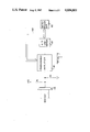
- FIG. 8 shows a portion of the programmable amplification circuit employed in the preferred embodiment of this invention, including an analog multiplexer-demultiplexer used as an analog switch and a sample and hold circuit.
- FIG. 9 shows the remainder of the programmable amplification means consisting of a dual digital to analog converter and a difference amplifier.
- FIG. 10 shows an analog to digital converter receiving preconditioned signals from the programmable amplifier and inputing a digitized signal into a digital microprocessor.
- an operator 16 can simply choose one of several alternative inputs displayed at various locations on a screen, and can perform other interactions with the display 12, such as cursor control.
- cursor control By using infrared emitters and detectors, the beam pattern established within the irradiated field will not optically interfere with the electronic display.
- a touch input system of this type can be employed either as an alternative to or in addition to a conventional keyboard 14.
- FIG. 2 shows a conventional optical matrix 20 comprising a plurality of emitters and detectors located around the periphery of an intermediate irradiated field.
- emitters are located along two sides of the rectangular matrix.
- Corresponding detectors are located along the opposite sides.
- a plurality of X emitters, X1, X2, . . . XN, are located along the lower surface of the opto matrix frame 20.
- These X emitters comprise conventional infrared light emitting diodes and are generally positioned on predetermined centerlines along the lower periphery of the frame.
- a plurality of Y emitters, Y1, Y2, . . . YN are located along the left side of the opto matrix frame 20.
- These Y emitters also comprise conventional infrared light emitting diodes and are spaced apart on the same centerlines.
- the X and Y emitters individually transmit beams within the irradiated field forming a grid of infrared beams
- a plurality of photodetectors, X1', X2', . . . XN', comprising a linear array of photodetectors are positioned along the top of frame 20.
- these X photodetectors, X1', X2', . . . XN' each comprise conventional infrared phototransistors.
- a similar linear array of Y photodetectors, Y1', Y2', . . . YN', are positioned along the right side of frame 20.
- emitter X1 and photodetector X1' are axially aligned as shown in FIG. 2.
- the opto matrix frame 20 comprises a printed circuit board having the emitters and detectors affixed thereto on precise centerlines. Even though associated emitter/detector pairs are axially aligned, the light incident on each detector cannot be confined to the light emitted from corresponding LED. As shown in FIG.
- FIG. 2 assumes that the light beams emitted from emitters such as X1 and Y1 are precisely centered around the axis of alignment between associated emitters and detectors. However, with conventional LEDs, such alignment cannot be maintained.
- FIG. 3 shows three side by side light emitting LEDs 101, 102, and 103. These LEDs 101, 102, and 103 can represent the light emitting patterns of LEDs arbitrarily distributed at any point within the emitter arrays. Although the emitters 101, 102, and 103 would be mechanically aligned along respective axis 101A, 102A, and 103A, the light emission pattern for each of these emitters would not be the same.
- the central emitter 102 shows a light emitting device having an on-axis optical dispersion. Light is evenly distributed around axis 102A as illustrated by a light envelope 102B. The strongest signal from LED 102 is coincident with the axis 102A and would, therefore, normally be incident upon a corresponding photodetector also aligned along axis 102A. LED 101, however, shows a conventional LED in which the optical intensity is not aligned with the geometrical axis 101A of the LED. Again, the envelope 101B, representative of the light emitted from LED 101, is along the axis 101A' rather than the axis 101A.
- the other axis of the infrared LED matrix is enabled using a 54LS145 4-line to 10-line binary coded decimal converter active low decoder U20.
- Decoder U20 is activated by the microprocessor through input signal lines BA, BB, BC, and BD. If only a single row and a single column is selected, only the single LED having that specific row and column address within the LED matrix will be activated in response to unique signals from the microprocessor.
- the matrix of photodetectors X1', X2', . . . XN' and Y1', Y2', . . . YN' are configured in a matrix as shown in FIG. 6 in a fashion similar to the emitter matrix. As shown in example of FIG. 6, the photodetectors are positioned in six rows and eight columns. Again, each individual phototransistor is sequentially selected by addressing the appropriate row and column corresponding to the unique address of the selected photodetector. Selection of the individual photodetectors is again controlled by the microprocesor.
- That quiescent voltage level, which is labeled QCSIG is fed in the common IO pin of device U11.
- the signal detected on each selected photodetector will be riding on top of the quiescent level on QCSIG.
- the signal QCSIG feeds one port of an AD7528 dual digital to analog converter U5 shown in FIG. 9.
- the photosignal at QCSIG also drives an IO input pin of a 54HC 40 53 analog multiplexer-demultiplexer U8 shown in FIG. 8.
- FIG. 7 is a schematic showing the elements for preconditioning a signal prior to transmission of that signal to an analog to digital converter.
- the signals QC0 to QC7 output from the photodetectors and input into the analog multiplexer U11 are output into a programmable amplifier 40.
- the amplified signals are in turn transmitted to an analog to digital converter 60.
- the digital signals from the analog to digital converter 60 are then transmitted to a microprocessor computing means 80.
- the microprocessor compares the digital signals received from A-D converter 60 with a normalized range of signals for each photodetector. If the signals transmitted to microprocessor 80 do not fall within a prescribed normalized range, the signal is transmitted along bus 100 to programmable amplifier 40 to provide amplification for each of the signals.
- FIG. 8 shows an analog switch and a hold circuit which comprises a part of the programmable amplifier 40 shown in FIG. 7.
- the analog multiplexer-demultiplexer U8, into which the photosignal QCSIG is input, is used as an analog switch.
- switch U8 When switch U8 is closed, the voltage on QCSIG resides on capacitor C33. With switch U8 closed, which occurs when LCSELD goes high, the signal that was on QCSIG will remain on C33 until the switch is again open.
- the TLC274A opamp U6 serves as a high impedance buffer for a capacitor C33.
- the output QCREF of the high impedance buffer and QCSIG are in turn input into an AD7528 non-buffered ladder-type dual digital to analog converter (DAC) U5.
- the dual digital to analog converter is used to feed a TLC274A opamp U7.
- This device is configured as a differential amplifier with a gain determined by the dual digital to analog converter and resistors R3 and R6. Appropriate selection of the values of resistors R3 and R6 gives an approximate range of gain of 1 to 256.
- the output AIN of the differential amplifier U7 shown in FIG. 9, is in turn input into an AD7576 analog to digital converter U9. This analog to digital converter converts the analog signal into a digital level value is read by the microprocessor 80.
Landscapes
- Engineering & Computer Science (AREA)
- Theoretical Computer Science (AREA)
- General Engineering & Computer Science (AREA)
- Physics & Mathematics (AREA)
- General Physics & Mathematics (AREA)
- Life Sciences & Earth Sciences (AREA)
- Human Computer Interaction (AREA)
- General Life Sciences & Earth Sciences (AREA)
- Geophysics (AREA)
- Position Input By Displaying (AREA)
- Length Measuring Devices By Optical Means (AREA)
- Geophysics And Detection Of Objects (AREA)
- Electronic Switches (AREA)
Priority Applications (6)
| Application Number | Priority Date | Filing Date | Title |
|---|---|---|---|
| US06/835,015 US4684801A (en) | 1986-02-28 | 1986-02-28 | Signal preconditioning for touch entry device |
| EP86309970A EP0239705B1 (de) | 1986-02-28 | 1986-12-19 | Signalvorbereitung für einen berührungsaktiven Bildschirm |
| DE8686309970T DE3680521D1 (de) | 1986-02-28 | 1986-12-19 | Signalvorbereitung fuer einen beruehrungsaktiven bildschirm. |
| JP62045105A JPS62206404A (ja) | 1986-02-28 | 1987-02-27 | タツチ式入力装置のための信号前処理 |
| SG100894A SG100894G (en) | 1986-02-28 | 1994-07-23 | Signal preconditioning for touch entry device |
| HK128394A HK128394A (en) | 1986-02-28 | 1994-11-17 | Signal preconditioning for touch entry device |
Applications Claiming Priority (1)
| Application Number | Priority Date | Filing Date | Title |
|---|---|---|---|
| US06/835,015 US4684801A (en) | 1986-02-28 | 1986-02-28 | Signal preconditioning for touch entry device |
Publications (1)
| Publication Number | Publication Date |
|---|---|
| US4684801A true US4684801A (en) | 1987-08-04 |
Family
ID=25268357
Family Applications (1)
| Application Number | Title | Priority Date | Filing Date |
|---|---|---|---|
| US06/835,015 Expired - Fee Related US4684801A (en) | 1986-02-28 | 1986-02-28 | Signal preconditioning for touch entry device |
Country Status (5)
| Country | Link |
|---|---|
| US (1) | US4684801A (de) |
| EP (1) | EP0239705B1 (de) |
| JP (1) | JPS62206404A (de) |
| DE (1) | DE3680521D1 (de) |
| HK (1) | HK128394A (de) |
Cited By (52)
| Publication number | Priority date | Publication date | Assignee | Title |
|---|---|---|---|---|
| US4855590A (en) * | 1987-06-25 | 1989-08-08 | Amp Incorporated | Infrared touch input device having ambient compensation |
| US4899138A (en) * | 1987-01-10 | 1990-02-06 | Pioneer Electronic Corporation | Touch panel control device with touch time and finger direction discrimination |
| US4905174A (en) * | 1987-09-07 | 1990-02-27 | Alps Electric Co., Ltd. | Optical coordinate input apparatus |
| US4904857A (en) * | 1986-01-13 | 1990-02-27 | Nippondenso Co., Ltd. | Electric control system for photoelectric touch input apparatus |
| WO1990003014A1 (en) * | 1988-09-02 | 1990-03-22 | Amp Incorporated | Touch entry system with ambient compensation and programmable amplification |
| US4916308A (en) * | 1988-10-17 | 1990-04-10 | Tektronix, Inc. | Integrated liquid crystal display and optical touch panel |
| US5025411A (en) * | 1986-12-08 | 1991-06-18 | Tektronix, Inc. | Method which provides debounced inputs from a touch screen panel by waiting until each x and y coordinates stop altering |
| US5107253A (en) * | 1989-11-13 | 1992-04-21 | Tektronix, Inc. | Stylus position detection system for optical touch panel |
| US5138468A (en) * | 1990-02-02 | 1992-08-11 | Dz Company | Keyless holographic lock |
| US5164714A (en) * | 1988-06-20 | 1992-11-17 | Amp Incorporated | Modulated touch entry system and method with synchronous detection |
| US5194863A (en) * | 1989-04-10 | 1993-03-16 | International Business Machines Corporation | Touch panel display |
| USD338656S (en) | 1991-07-02 | 1993-08-24 | Tusk, Incorporated | Workslate computer unit |
| US5341133A (en) * | 1991-05-09 | 1994-08-23 | The Rowland Institute For Science, Inc. | Keyboard having touch sensor keys for conveying information electronically |
| US5577848A (en) * | 1992-08-24 | 1996-11-26 | Bowen; James H. | Light controlled touch pad for cursor and selection control on a computer display |
| US5577733A (en) * | 1994-04-08 | 1996-11-26 | Downing; Dennis L. | Targeting system |
| US5605406A (en) * | 1992-08-24 | 1997-02-25 | Bowen; James H. | Computer input devices with light activated switches and light emitter protection |
| US5635724A (en) * | 1995-06-07 | 1997-06-03 | Intecolor | Method and apparatus for detecting the location of an object on a surface |
| US5796389A (en) * | 1994-08-22 | 1998-08-18 | International Game Technology | Reduced noise touch screen apparatus and method |
| GB2359233A (en) * | 1999-11-24 | 2001-08-15 | Namco Ltd | Controlling an on-screen display using received light pattern detection apparatus |
| US6278443B1 (en) * | 1998-04-30 | 2001-08-21 | International Business Machines Corporation | Touch screen with random finger placement and rolling on screen to control the movement of information on-screen |
| US6316777B1 (en) * | 1999-04-02 | 2001-11-13 | Indigo Systems Corporation | Constant power snapshot microemitter array with integral digital interface, isolated substrate current return, and linearized signal response |
| US6597347B1 (en) | 1991-11-26 | 2003-07-22 | Itu Research Inc. | Methods and apparatus for providing touch-sensitive input in multiple degrees of freedom |
| US20040135107A1 (en) * | 2003-01-15 | 2004-07-15 | Bennewitz Hans Jurgen | Light image sensor test of opto-electronics for in-circuit test |
| US20050152146A1 (en) * | 2002-05-08 | 2005-07-14 | Owen Mark D. | High efficiency solid-state light source and methods of use and manufacture |
| US20050230600A1 (en) * | 2004-03-30 | 2005-10-20 | Olson Steven J | LED array having array-based LED detectors |
| US20050231713A1 (en) * | 2004-04-19 | 2005-10-20 | Owen Mark D | Imaging semiconductor structures using solid state illumination |
| US20060188198A1 (en) * | 2004-12-09 | 2006-08-24 | Rpo Pty Limited | Optical power distribution devices |
| US20060216865A1 (en) * | 2004-03-18 | 2006-09-28 | Phoseon Technology, Inc. | Direct cooling of leds |
| US20070030678A1 (en) * | 2003-10-31 | 2007-02-08 | Phoseon Technology, Inc. | Series wiring of highly reliable light sources |
| US20070051964A1 (en) * | 2004-04-12 | 2007-03-08 | Owen Mark D | High density led array |
| US20070080956A1 (en) * | 2005-10-07 | 2007-04-12 | Integrated Digital Technologies, Inc. | Interactive Display Devices And Methods Of Making The Same |
| US20070109790A1 (en) * | 2003-10-31 | 2007-05-17 | Phoseon Technology, Inc. | Collection optics for led array with offset hemispherical or faceted surfaces |
| US20070154823A1 (en) * | 2005-12-30 | 2007-07-05 | Phoseon Technology, Inc. | Multi-attribute light effects for use in curing and other applications involving photoreactions and processing |
| US20080087796A1 (en) * | 2006-09-25 | 2008-04-17 | Integrated Digital Technologies, Inc. | Photo detector array with thin-film resistor-capacitor network |
| US7461949B2 (en) | 2002-05-08 | 2008-12-09 | Phoseon Technology, Inc. | Methods and systems relating to solid state light sources for use in industrial processes |
| USRE40891E1 (en) | 1991-11-26 | 2009-09-01 | Sandio Technology Corp. | Methods and apparatus for providing touch-sensitive input in multiple degrees of freedom |
| US7638808B2 (en) | 2004-03-18 | 2009-12-29 | Phoseon Technology, Inc. | Micro-reflectors on a substrate for high-density LED array |
| US20100020040A1 (en) * | 2004-10-22 | 2010-01-28 | New York University | Multi-touch sensing light emitting diode display and method for using the same |
| US20110018840A1 (en) * | 2005-10-07 | 2011-01-27 | Integrated Digital Technologies, Inc. | Touch screen system |
| US20110069038A1 (en) * | 2005-10-07 | 2011-03-24 | Sen-Shyong Fann | Interactive display panel |
| US20110090194A1 (en) * | 2005-10-07 | 2011-04-21 | Yang-Hui Chang | Pixel array and display panel having the same |
| US20110157095A1 (en) * | 2008-08-07 | 2011-06-30 | Owen Drumm | Optical Control System With Feedback Control |
| US20110157096A1 (en) * | 2008-08-07 | 2011-06-30 | Owen Drumm | Method and Apparatus For Detecting A Multitouch Event In An Optical Touch-Sensitive Device |
| US8264468B1 (en) | 2007-06-19 | 2012-09-11 | Imaging Systems Technology, Inc. | Touch system for blue screen |
| US8330730B1 (en) | 2007-09-04 | 2012-12-11 | Imaging Systems Technology, Inc. | Calibrating of interactive touch system for image compositing |
| US8461512B2 (en) | 2008-08-07 | 2013-06-11 | Rapt Ip Limited | Optical control system with modulated emitters |
| US9170683B2 (en) | 2011-07-22 | 2015-10-27 | Rapt Ip Limited | Optical coupler for use in an optical touch sensitive device |
| EP2866520A4 (de) * | 2012-06-26 | 2015-12-16 | Institucion Universitaria Colegio Mayor De Antioquia | Multiplex-led-leuchte mit extrem niedrigen energieverbrauch |
| US9524060B2 (en) | 2012-07-13 | 2016-12-20 | Rapt Ip Limited | Low power operation of an optical touch-sensitive device for detecting multitouch events |
| US9552104B2 (en) | 2008-08-07 | 2017-01-24 | Rapt Ip Limited | Detecting multitouch events in an optical touch-sensitive device using touch event templates |
| US11625128B2 (en) | 2020-04-03 | 2023-04-11 | 1004335 Ontario Inc. | Optical touch sensor systems and optical detectors with noise mitigation |
| US11893188B2 (en) | 2018-05-18 | 2024-02-06 | 1004335 Ontario Inc. | Optical touch sensor devices and systems |
Families Citing this family (6)
| Publication number | Priority date | Publication date | Assignee | Title |
|---|---|---|---|---|
| JPH01314324A (ja) * | 1988-06-14 | 1989-12-19 | Sony Corp | タッチパネル装置 |
| EP0450203A3 (en) * | 1989-04-10 | 1991-11-21 | International Business Machines Corporation | Touch panel display |
| EP0438057B1 (de) * | 1990-01-16 | 1996-10-23 | Carroll Touch Incorporated | Infrarotberührungsempfindliche Eingabevorrichtung und Lichterzeugeraktivierungsschaltung |
| CH681756A5 (de) * | 1990-11-12 | 1993-05-14 | Beat Decoi | |
| WO2000029870A1 (de) * | 1998-11-16 | 2000-05-25 | Siemens Aktiengesellschaft | Optischer näherungsschalter |
| US7423227B2 (en) * | 2003-09-04 | 2008-09-09 | Avago Technologies Ecbu Ip Pte Ltd | Apparatus for optical navigation |
Citations (3)
| Publication number | Priority date | Publication date | Assignee | Title |
|---|---|---|---|---|
| US4459476A (en) * | 1982-01-19 | 1984-07-10 | Zenith Radio Corporation | Co-ordinate detection system |
| US4590410A (en) * | 1979-05-31 | 1986-05-20 | Joensson Bert Ove | Object sensing apparatus |
| US4591710A (en) * | 1983-07-11 | 1986-05-27 | Electro Mechanical Systems, Inc. | Ambient light and electromagnetic noise reduction circuit |
Family Cites Families (6)
| Publication number | Priority date | Publication date | Assignee | Title |
|---|---|---|---|---|
| US4097731A (en) * | 1977-06-02 | 1978-06-27 | Burroughs Corporation | Automatic gain control for photosensing devices |
| US4243879A (en) * | 1978-04-24 | 1981-01-06 | Carroll Manufacturing Corporation | Touch panel with ambient light sampling |
| CA1187959A (en) * | 1981-11-06 | 1985-05-28 | Kalervo Virtanen | Signalling device for vehicles |
| US4559452A (en) * | 1982-06-02 | 1985-12-17 | Fujitsu Limited | Apparatus for detecting edge of semitransparent plane substance |
| JPS5970990A (ja) * | 1982-10-18 | 1984-04-21 | Ricoh Co Ltd | 調光方法 |
| DE3408261A1 (de) * | 1984-03-07 | 1985-09-19 | Hansa Metallwerke Ag, 7000 Stuttgart | Annaeherungsschalter sowie steuerschaltungsanordnung hierfuer |
-
1986
- 1986-02-28 US US06/835,015 patent/US4684801A/en not_active Expired - Fee Related
- 1986-12-19 DE DE8686309970T patent/DE3680521D1/de not_active Expired - Fee Related
- 1986-12-19 EP EP86309970A patent/EP0239705B1/de not_active Expired
-
1987
- 1987-02-27 JP JP62045105A patent/JPS62206404A/ja active Pending
-
1994
- 1994-11-17 HK HK128394A patent/HK128394A/en not_active IP Right Cessation
Patent Citations (3)
| Publication number | Priority date | Publication date | Assignee | Title |
|---|---|---|---|---|
| US4590410A (en) * | 1979-05-31 | 1986-05-20 | Joensson Bert Ove | Object sensing apparatus |
| US4459476A (en) * | 1982-01-19 | 1984-07-10 | Zenith Radio Corporation | Co-ordinate detection system |
| US4591710A (en) * | 1983-07-11 | 1986-05-27 | Electro Mechanical Systems, Inc. | Ambient light and electromagnetic noise reduction circuit |
Cited By (93)
| Publication number | Priority date | Publication date | Assignee | Title |
|---|---|---|---|---|
| US4904857A (en) * | 1986-01-13 | 1990-02-27 | Nippondenso Co., Ltd. | Electric control system for photoelectric touch input apparatus |
| US5025411A (en) * | 1986-12-08 | 1991-06-18 | Tektronix, Inc. | Method which provides debounced inputs from a touch screen panel by waiting until each x and y coordinates stop altering |
| US4899138A (en) * | 1987-01-10 | 1990-02-06 | Pioneer Electronic Corporation | Touch panel control device with touch time and finger direction discrimination |
| US4855590A (en) * | 1987-06-25 | 1989-08-08 | Amp Incorporated | Infrared touch input device having ambient compensation |
| US4905174A (en) * | 1987-09-07 | 1990-02-27 | Alps Electric Co., Ltd. | Optical coordinate input apparatus |
| US5164714A (en) * | 1988-06-20 | 1992-11-17 | Amp Incorporated | Modulated touch entry system and method with synchronous detection |
| US4988983A (en) * | 1988-09-02 | 1991-01-29 | Carroll Touch, Incorporated | Touch entry system with ambient compensation and programmable amplification |
| WO1990003014A1 (en) * | 1988-09-02 | 1990-03-22 | Amp Incorporated | Touch entry system with ambient compensation and programmable amplification |
| US4916308A (en) * | 1988-10-17 | 1990-04-10 | Tektronix, Inc. | Integrated liquid crystal display and optical touch panel |
| US5194863A (en) * | 1989-04-10 | 1993-03-16 | International Business Machines Corporation | Touch panel display |
| US5107253A (en) * | 1989-11-13 | 1992-04-21 | Tektronix, Inc. | Stylus position detection system for optical touch panel |
| US5138468A (en) * | 1990-02-02 | 1992-08-11 | Dz Company | Keyless holographic lock |
| US5341133A (en) * | 1991-05-09 | 1994-08-23 | The Rowland Institute For Science, Inc. | Keyboard having touch sensor keys for conveying information electronically |
| USD338656S (en) | 1991-07-02 | 1993-08-24 | Tusk, Incorporated | Workslate computer unit |
| US6597347B1 (en) | 1991-11-26 | 2003-07-22 | Itu Research Inc. | Methods and apparatus for providing touch-sensitive input in multiple degrees of freedom |
| USRE40891E1 (en) | 1991-11-26 | 2009-09-01 | Sandio Technology Corp. | Methods and apparatus for providing touch-sensitive input in multiple degrees of freedom |
| US5605406A (en) * | 1992-08-24 | 1997-02-25 | Bowen; James H. | Computer input devices with light activated switches and light emitter protection |
| US5577848A (en) * | 1992-08-24 | 1996-11-26 | Bowen; James H. | Light controlled touch pad for cursor and selection control on a computer display |
| US5988645A (en) * | 1994-04-08 | 1999-11-23 | Downing; Dennis L. | Moving object monitoring system |
| US5577733A (en) * | 1994-04-08 | 1996-11-26 | Downing; Dennis L. | Targeting system |
| US5796389A (en) * | 1994-08-22 | 1998-08-18 | International Game Technology | Reduced noise touch screen apparatus and method |
| US6476798B1 (en) | 1994-08-22 | 2002-11-05 | International Game Technology | Reduced noise touch screen apparatus and method |
| US6734843B2 (en) | 1994-08-22 | 2004-05-11 | Igt | Reduced noise touch screen apparatus and method |
| US5635724A (en) * | 1995-06-07 | 1997-06-03 | Intecolor | Method and apparatus for detecting the location of an object on a surface |
| US6278443B1 (en) * | 1998-04-30 | 2001-08-21 | International Business Machines Corporation | Touch screen with random finger placement and rolling on screen to control the movement of information on-screen |
| US6316777B1 (en) * | 1999-04-02 | 2001-11-13 | Indigo Systems Corporation | Constant power snapshot microemitter array with integral digital interface, isolated substrate current return, and linearized signal response |
| GB2359233A (en) * | 1999-11-24 | 2001-08-15 | Namco Ltd | Controlling an on-screen display using received light pattern detection apparatus |
| US6798402B1 (en) | 1999-11-24 | 2004-09-28 | Namco, Ltd. | Received-light pattern detection apparatus |
| US20050152146A1 (en) * | 2002-05-08 | 2005-07-14 | Owen Mark D. | High efficiency solid-state light source and methods of use and manufacture |
| US10401012B2 (en) | 2002-05-08 | 2019-09-03 | Phoseon Technology, Inc. | High efficiency solid-state light source and methods of use and manufacture |
| US8496356B2 (en) | 2002-05-08 | 2013-07-30 | Phoseon Technology, Inc. | High efficiency solid-state light source and methods of use and manufacture |
| US8192053B2 (en) | 2002-05-08 | 2012-06-05 | Phoseon Technology, Inc. | High efficiency solid-state light source and methods of use and manufacture |
| US7461949B2 (en) | 2002-05-08 | 2008-12-09 | Phoseon Technology, Inc. | Methods and systems relating to solid state light sources for use in industrial processes |
| US6956226B2 (en) * | 2003-01-15 | 2005-10-18 | Hewlett-Packard Development Company, L.P. | Light image sensor test of opto-electronics for in-circuit test |
| US20040135107A1 (en) * | 2003-01-15 | 2004-07-15 | Bennewitz Hans Jurgen | Light image sensor test of opto-electronics for in-circuit test |
| US7524085B2 (en) | 2003-10-31 | 2009-04-28 | Phoseon Technology, Inc. | Series wiring of highly reliable light sources |
| US8523387B2 (en) | 2003-10-31 | 2013-09-03 | Phoseon Technology, Inc. | Collection optics for LED array with offset hemispherical or faceted surfaces |
| US20070030678A1 (en) * | 2003-10-31 | 2007-02-08 | Phoseon Technology, Inc. | Series wiring of highly reliable light sources |
| US20070109790A1 (en) * | 2003-10-31 | 2007-05-17 | Phoseon Technology, Inc. | Collection optics for led array with offset hemispherical or faceted surfaces |
| US7819550B2 (en) | 2003-10-31 | 2010-10-26 | Phoseon Technology, Inc. | Collection optics for led array with offset hemispherical or faceted surfaces |
| US20110063840A1 (en) * | 2003-10-31 | 2011-03-17 | Phoseon Technology, Inc. | Collection optics for led array with offset hemispherical or faceted surfaces |
| US7235878B2 (en) | 2004-03-18 | 2007-06-26 | Phoseon Technology, Inc. | Direct cooling of LEDs |
| US7285445B2 (en) | 2004-03-18 | 2007-10-23 | Phoseon Technology, Inc. | Direct cooling of LEDs |
| US8637332B2 (en) | 2004-03-18 | 2014-01-28 | Phoseon Technology, Inc. | Micro-reflectors on a substrate for high-density LED array |
| US20060216865A1 (en) * | 2004-03-18 | 2006-09-28 | Phoseon Technology, Inc. | Direct cooling of leds |
| US20100052002A1 (en) * | 2004-03-18 | 2010-03-04 | Phoseon Technology, Inc. | Micro-reflectors on a substrate for high-density led array |
| US7638808B2 (en) | 2004-03-18 | 2009-12-29 | Phoseon Technology, Inc. | Micro-reflectors on a substrate for high-density LED array |
| US20050230600A1 (en) * | 2004-03-30 | 2005-10-20 | Olson Steven J | LED array having array-based LED detectors |
| WO2005094390A3 (en) * | 2004-03-30 | 2006-11-30 | Phoseon Technology Inc | Led array having array-based led detectors |
| US7816638B2 (en) | 2004-03-30 | 2010-10-19 | Phoseon Technology, Inc. | LED array having array-based LED detectors |
| US20070051964A1 (en) * | 2004-04-12 | 2007-03-08 | Owen Mark D | High density led array |
| US8077305B2 (en) | 2004-04-19 | 2011-12-13 | Owen Mark D | Imaging semiconductor structures using solid state illumination |
| US20050231713A1 (en) * | 2004-04-19 | 2005-10-20 | Owen Mark D | Imaging semiconductor structures using solid state illumination |
| US20100020040A1 (en) * | 2004-10-22 | 2010-01-28 | New York University | Multi-touch sensing light emitting diode display and method for using the same |
| US9787324B2 (en) * | 2004-10-22 | 2017-10-10 | New York University | Multi-touch sensing light emitting diode display and method for using the same |
| US20090233003A1 (en) * | 2004-11-08 | 2009-09-17 | Phoseon Technology, Inc. | Methods and systems relating to light sources for use in industrial processes |
| US9281001B2 (en) | 2004-11-08 | 2016-03-08 | Phoseon Technology, Inc. | Methods and systems relating to light sources for use in industrial processes |
| US7421167B2 (en) | 2004-12-09 | 2008-09-02 | Rpo Pty Limited | Optical power distribution devices |
| US20060188198A1 (en) * | 2004-12-09 | 2006-08-24 | Rpo Pty Limited | Optical power distribution devices |
| US9064772B2 (en) | 2005-10-07 | 2015-06-23 | Integrated Digital Technologies, Inc. | Touch screen system having dual touch sensing function |
| US20110069038A1 (en) * | 2005-10-07 | 2011-03-24 | Sen-Shyong Fann | Interactive display panel |
| US8575536B2 (en) | 2005-10-07 | 2013-11-05 | Integrated Digital Technologies Inc. | Pixel array and touch sensing display panel having the same |
| US20070080956A1 (en) * | 2005-10-07 | 2007-04-12 | Integrated Digital Technologies, Inc. | Interactive Display Devices And Methods Of Making The Same |
| US8537149B2 (en) | 2005-10-07 | 2013-09-17 | Integrated Digital Technologies, Inc. | Pixel array and display panel having the same |
| US20110018840A1 (en) * | 2005-10-07 | 2011-01-27 | Integrated Digital Technologies, Inc. | Touch screen system |
| US20110096026A1 (en) * | 2005-10-07 | 2011-04-28 | Sen-Shyong Fann | Pixel array and display panel having the same |
| US20110090194A1 (en) * | 2005-10-07 | 2011-04-21 | Yang-Hui Chang | Pixel array and display panel having the same |
| US8748796B2 (en) | 2005-10-07 | 2014-06-10 | Integrated Digital Technologies, Inc. | Interactive display panel having touch-sensing functions |
| US7935917B2 (en) | 2005-10-07 | 2011-05-03 | Integrated Digital Technologies, Inc. | Photo detector device having multiple photosensitive transistors |
| US20090179243A1 (en) * | 2005-10-07 | 2009-07-16 | Integrated Digital Technologies, Inc. | Photo detector array |
| US7642527B2 (en) | 2005-12-30 | 2010-01-05 | Phoseon Technology, Inc. | Multi-attribute light effects for use in curing and other applications involving photoreactions and processing |
| US20070154823A1 (en) * | 2005-12-30 | 2007-07-05 | Phoseon Technology, Inc. | Multi-attribute light effects for use in curing and other applications involving photoreactions and processing |
| US20080087796A1 (en) * | 2006-09-25 | 2008-04-17 | Integrated Digital Technologies, Inc. | Photo detector array with thin-film resistor-capacitor network |
| EP1903788B1 (de) * | 2006-09-25 | 2011-09-07 | Integrated Digital Technologies | Photodetektoranordnung |
| US7960679B2 (en) | 2006-09-25 | 2011-06-14 | Integrated Digital Technologies, Inc. | Photo detector array with thin-film resistor-capacitor network for use with a display device |
| US8264468B1 (en) | 2007-06-19 | 2012-09-11 | Imaging Systems Technology, Inc. | Touch system for blue screen |
| US8330730B1 (en) | 2007-09-04 | 2012-12-11 | Imaging Systems Technology, Inc. | Calibrating of interactive touch system for image compositing |
| US20110157095A1 (en) * | 2008-08-07 | 2011-06-30 | Owen Drumm | Optical Control System With Feedback Control |
| US10067609B2 (en) | 2008-08-07 | 2018-09-04 | Rapt Ip Limited | Detecting multitouch events in an optical touch-sensitive device using touch event templates |
| US9086762B2 (en) | 2008-08-07 | 2015-07-21 | Rapt Ip Limited | Optical control system with modulated emitters |
| US9335864B2 (en) | 2008-08-07 | 2016-05-10 | Rapt Ip Limited | Method and apparatus for detecting a multitouch event in an optical touch-sensitive device |
| US8350831B2 (en) | 2008-08-07 | 2013-01-08 | Rapt Ip Limited | Method and apparatus for detecting a multitouch event in an optical touch-sensitive device |
| US8426799B2 (en) | 2008-08-07 | 2013-04-23 | Rapt Ip Limited | Optical control system with feedback control |
| US20110157096A1 (en) * | 2008-08-07 | 2011-06-30 | Owen Drumm | Method and Apparatus For Detecting A Multitouch Event In An Optical Touch-Sensitive Device |
| US9552104B2 (en) | 2008-08-07 | 2017-01-24 | Rapt Ip Limited | Detecting multitouch events in an optical touch-sensitive device using touch event templates |
| US8461512B2 (en) | 2008-08-07 | 2013-06-11 | Rapt Ip Limited | Optical control system with modulated emitters |
| US9170683B2 (en) | 2011-07-22 | 2015-10-27 | Rapt Ip Limited | Optical coupler for use in an optical touch sensitive device |
| EP2866520A4 (de) * | 2012-06-26 | 2015-12-16 | Institucion Universitaria Colegio Mayor De Antioquia | Multiplex-led-leuchte mit extrem niedrigen energieverbrauch |
| US9916041B2 (en) | 2012-07-13 | 2018-03-13 | Rapt Ip Limited | Low power operation of an optical touch-sensitive device for detecting multitouch events |
| US9524060B2 (en) | 2012-07-13 | 2016-12-20 | Rapt Ip Limited | Low power operation of an optical touch-sensitive device for detecting multitouch events |
| US11893188B2 (en) | 2018-05-18 | 2024-02-06 | 1004335 Ontario Inc. | Optical touch sensor devices and systems |
| US11625128B2 (en) | 2020-04-03 | 2023-04-11 | 1004335 Ontario Inc. | Optical touch sensor systems and optical detectors with noise mitigation |
| US11630536B2 (en) | 2020-04-03 | 2023-04-18 | 1004335 Ontario Inc. | Optical touch sensor systems and optical detectors with noise mitigation |
Also Published As
| Publication number | Publication date |
|---|---|
| EP0239705A1 (de) | 1987-10-07 |
| EP0239705B1 (de) | 1991-07-24 |
| JPS62206404A (ja) | 1987-09-10 |
| DE3680521D1 (de) | 1991-08-29 |
| HK128394A (en) | 1994-11-25 |
Similar Documents
| Publication | Publication Date | Title |
|---|---|---|
| US4684801A (en) | Signal preconditioning for touch entry device | |
| KR0128736B1 (ko) | 터치입력 시스템 | |
| US4703316A (en) | Touch panel input apparatus | |
| EP0095948B1 (de) | Detektieren der Kanten von Gegenständen | |
| CA1225723A (en) | Touch sensitive device | |
| US4311990A (en) | Photo-optical keyboards | |
| US4737631A (en) | Filter of photoelectric touch panel with integral spherical protrusion lens | |
| US3648050A (en) | Optoelectronic data entry means having plurality of control means to direct part of radiation in channel from radiation source to output channel | |
| JPH0231415B2 (de) | ||
| US8400406B1 (en) | IR touch | |
| US5886776A (en) | Laser beam receiver circuit | |
| SE457151B (sv) | Anordning foer optisk avkaenning av foeremaal | |
| US9865764B2 (en) | Image capture device with integrated illumination and method for producing the device | |
| JPH0612512B2 (ja) | 光学式タッチパネルの受光素子の感度調整方法 | |
| JPS6416902A (en) | Tactile sensor | |
| US6100822A (en) | Optical sensing system using multiple detectors at various positions for generating position signals | |
| US9013450B1 (en) | IR touch | |
| EP0438057B1 (de) | Infrarotberührungsempfindliche Eingabevorrichtung und Lichterzeugeraktivierungsschaltung | |
| US3223845A (en) | Optical transducer for measuring distance | |
| JPS6165760A (ja) | 生産指示装置 | |
| RU2003100999A (ru) | Устройство для ввода информации | |
| JPS5963808A (ja) | 増幅回路 | |
| JPS6376012A (ja) | 座標位置入力装置 | |
| JP2603362Y2 (ja) | 非接触型位置検出装置 | |
| JPH0315920A (ja) | 座標入力装置 |
Legal Events
| Date | Code | Title | Description |
|---|---|---|---|
| AS | Assignment |
Owner name: CARROLL TOUCH, INC., TEXAS Free format text: ASSIGNMENT OF ASSIGNORS INTEREST;ASSIGNORS:CARROLL, ARTHUR B.;HOUGH, STEWART E.;HUNTER, PAUL R.;AND OTHERS;SIGNING DATES FROM 19860305 TO 19860306;REEL/FRAME:004549/0982 Owner name: CARROLL TOUCH, INC., PO BOX 1309, ROUND ROCK, TEXA Free format text: ASSIGNMENT OF ASSIGNORS INTEREST.;ASSIGNORS:CARROLL, ARTHUR B.;HOUGH, STEWART E.;HUNTER, PAUL R.;AND OTHERS;REEL/FRAME:004549/0982;SIGNING DATES FROM 19860305 TO 19860306 |
|
| FEPP | Fee payment procedure |
Free format text: PAYOR NUMBER ASSIGNED (ORIGINAL EVENT CODE: ASPN); ENTITY STATUS OF PATENT OWNER: LARGE ENTITY |
|
| FPAY | Fee payment |
Year of fee payment: 4 |
|
| FEPP | Fee payment procedure |
Free format text: PAYOR NUMBER ASSIGNED (ORIGINAL EVENT CODE: ASPN); ENTITY STATUS OF PATENT OWNER: LARGE ENTITY Free format text: PAYER NUMBER DE-ASSIGNED (ORIGINAL EVENT CODE: RMPN); ENTITY STATUS OF PATENT OWNER: LARGE ENTITY |
|
| FPAY | Fee payment |
Year of fee payment: 8 |
|
| REMI | Maintenance fee reminder mailed | ||
| LAPS | Lapse for failure to pay maintenance fees | ||
| FP | Lapsed due to failure to pay maintenance fee |
Effective date: 19990804 |
|
| STCH | Information on status: patent discontinuation |
Free format text: PATENT EXPIRED DUE TO NONPAYMENT OF MAINTENANCE FEES UNDER 37 CFR 1.362 |