US4635232A - Semiconductor memory device - Google Patents
Semiconductor memory device Download PDFInfo
- Publication number
- US4635232A US4635232A US06/477,880 US47788083A US4635232A US 4635232 A US4635232 A US 4635232A US 47788083 A US47788083 A US 47788083A US 4635232 A US4635232 A US 4635232A
- Authority
- US
- United States
- Prior art keywords
- main memory
- transistor
- memory word
- gate
- word line
- Prior art date
- Legal status (The legal status is an assumption and is not a legal conclusion. Google has not performed a legal analysis and makes no representation as to the accuracy of the status listed.)
- Expired - Lifetime
Links
Images






Classifications
-
- G—PHYSICS
- G11—INFORMATION STORAGE
- G11C—STATIC STORES
- G11C29/00—Checking stores for correct operation ; Subsequent repair; Testing stores during standby or offline operation
- G11C29/70—Masking faults in memories by using spares or by reconfiguring
- G11C29/78—Masking faults in memories by using spares or by reconfiguring using programmable devices
- G11C29/785—Masking faults in memories by using spares or by reconfiguring using programmable devices with redundancy programming schemes
-
- G—PHYSICS
- G11—INFORMATION STORAGE
- G11C—STATIC STORES
- G11C29/00—Checking stores for correct operation ; Subsequent repair; Testing stores during standby or offline operation
- G11C29/70—Masking faults in memories by using spares or by reconfiguring
- G11C29/78—Masking faults in memories by using spares or by reconfiguring using programmable devices
- G11C29/83—Masking faults in memories by using spares or by reconfiguring using programmable devices with reduced power consumption
Definitions
- the present invention relates to semiconductor memory devices with improved production yields.
- One of the successful measures employs a memory device with a redundancy function. Specifically, an auxiliary memory is used in addition to a main memory. When the main memory contains an error bit cell, a drive or select line, on which bit cells including the error bit are arranged, is selected and all of the bit cells including the error bit cell are replaced with the correct bit cells arrayed on a select line of the auxiliary memory.
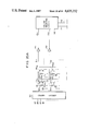
- FIG. 1 shows in block form an example of such a semiconductor memory device.
- reference numeral 1 designates an address buffer whose output is applied to a main address decoder 2 and an auxiliary decoder 3.
- the output signal from the main address decoder 2 is applied to a main memory 4 to select one of the row lines in the main memory 4. Subsequently, data may be written, by a write signal, into specified memory bit cells connected to the selected row line. Similarly, the data may be read out therefrom by a read signal.
- the main address decoder 2 is controlled by an output signal from the auxiliary address decoder 3.
- the decoder output of the auxiliary address decoder 3 is applied to an auxiliary memory 5. The signal selects one row line of the auxiliary memory 5.
- auxiliary address decoder 3 is programmed so as to produce an output signal representing an address of a memory area containing an error bit cell in the main memory.
- a control signal generating circuit 6 generates a control signal for the auxiliary memory 5 when an error bit cell is found in the main memory 4.
- the control signal controls the auxiliary address decoder 3 so as to replace a specific number of bit cells including the error bit cell with the corresponding number of correct bit cells in the auxiliary memory 5.
- the specific number of bit cells are those arrayed on a select or drive line, having the error bit cell connected thereto, of the main or auxiliary memory.
- This circuit 6 is composed of a nonvolatile memory, so programmed that it drives the auxiliary address decoder 3 to access the auxiliary memory 5 when the error bit cell is found.
- the control signal generating circuit 6 drives the auxiliary address decoder 3 to access the auxiliary memory 5, and at the same time to stop the operation of the main address decoder 2. In this way, the error bit cell in the main memory 4 is replaced with the correct bit cell of the auxiliary memory 5.
- FIGS. 2A and 2B show practical circuit diagrams of two examples of the control signal generator 6.
- a fuse element F made of polysilicon or the like is inserted between a potential source VD and an output terminal Out.
- An enhancement type MOS transistor 7 is connected between the output terminal Out and a ground.
- a depletion type MOS transistor 8 is inserted between the output terminal Out and a ground.
- a programming signal P is applied to the gate of the MOS transistor 7.
- the gate of the MOS transistor 8 is connected to a ground.
- the potential source VD and the output terminal Out have a programming enhancement type MOS transistor 7 and a depletion type MOS transistor 8, which are connected in parallel therebetween.
- a fuse element F is inserted between the output terminal Out and a ground.
- a programming signal P is applied to the gate of the MOS transistor 7 and the gate of the MOS transistor 8 is connected to the output terminal Out.
- the signal at the output terminal Out, or the control signal from the control signal generator 6, is logical "1", for example, and at this time the decoding operation of the auxiliary address decoder 3 stops.
- the decoding operation is performed only when the signal at the output terminal Out is logical "0".
- FIG. 3 shows a circuit diagram of an example of the auxiliary address decoder 3 when the control signal generator 6 is not used.
- the auxiliary address decoder 3 is comprised of a depletion type MOS transistor 9 for a load, a plurality of enhancement type MOS transistors 10 for driving the auxiliary memory whose gates are coupled with an address signal or data A 0 , A 0 , . . . , A n , A n , and a plurality of fuse elements F B inserted between each of the transistors 10 and the transistor 9.
- auxiliary address decoder 3 in order to access the auxiliary memory 5, a plurality of fuse elements F B must be burned out, which are selected according to the code of the address signal applied thereto.
- a laser beam or Joule heat is used to burn out these fuse elements.
- This burning means has some problems, however: welded material attached to its peripheral circuit reduces the reliability of the memory device, the failure of burning causes erroneous programming, and reliability on the burned locations is poor. In this respect, it is evident that the fewer the burning locations of the fuse elements, the better.
- memory capacity has increased together with the number of bits of an address input signal. Accordingly, the number of fuse elements burned out in the auxiliary memory also increases. For this reason, there is a pressing need to solve the above problems.
- This invention has been created in light of the above, and its object is to provide a semiconductor memory device which permits switching of the main memory over to the auxiliary memory if the main memory has an error bit cell by a simple operation, and thus permits improvement of the yield.
- a semiconductor memory device comprising:
- selecting means connected between said auxiliary memory and said decoder for selecting said auxiliary memory according to the output of said decoder;
- control means for controlling said selecting means.
- a semiconductor memory device comprising:
- circuit means operable according to the outputs of said column and row decoders to select said auxiliary memory when said main memory has an error bit cell.
- FIG. 1 is a block diagram showing a prior art semiconductor memory device having an auxiliary memory
- FIGS. 2A and 2B are circuit diagrams showing respective arrangements of a control signal generator incorporated in the semiconductor memory device shown in FIG. 1;
- FIG. 3 is a circuit diagram showing a decoder circuit for an auxiliary memory in the prior art
- FIG. 4 is a schematic representation of one embodiment of the semiconductor memory device according to the invention.
- FIG. 5 is a circuit diagram showing a modification of a control circuit used in the embodiment of FIG. 4;
- FIG. 6 is a circuit diagram showing a modification of the control circuit of FIG. 5 having an additional function of reducing power consumption
- FIG. 7 is a circuit diagram showing a further modification of the control circuit in the embodiment of FIG. 4 having an additional function of reducing power consumption;
- FIG. 8 is a circuit diagram showing a circuit arrangement, which includes the control circuit of the embodiment of FIG. 4 and a circuit for burning out a fuse element;
- FIG. 9 is a circuit diagram showing a circuit arrangement, which includes the control circuit of the embodiment of FIG. 4 and has the functions of burning out a fuse element and reducing power consumption;
- FIG. 10 is a circuit diagram showing a buffer circuit in the embodiment of FIG. 4;
- FIG. 11 is a schematic representation of a different embodiment of the semiconductor device according to the invention.
- FIG. 12 is a circuit diagram showing a modification of a control circuit in the embodiment of FIG. 4;
- FIG. 13 is a circuit diagram showing an inverter in the embodiment of FIG. 11;
- FIG. 14 is a circuit diagram showing a buffer circuit in the embodiment of FIG. 11;
- FIG. 15 is a circuit diagram showing a circuit arrangement including the control circuit in the embodiment of FIG. 11;
- FIG. 16 is a circuit diagram showing a modification of the circuit arrangement of FIG. 15;
- FIG. 17 is a schematic representation of a further embodiment of the semiconductor memory device according to the invention.
- FIG. 18 is a circuit diagram showing a buffer circuit in the embodiment of FIG. 17;
- FIG. 19 is a circuit, diagram showing a buffer circuit in the embodiment of FIG. 17;
- FIGS. 20A and 20B are schematic representations of a still further embodiment of the semiconductor memory device according to the invention.
- FIG. 21 is a circuit diagram showing an auxiliary memory selecting circuit in the embodiment of FIG. 20;
- FIG. 22 is view showing a modification of a circuit arrangement including a control circuit in the embodiment of FIG. 20;
- FIG. 23 is a circuit diagram showing an auxiliary memory selecting circuit suited for use with the circuit arrangement of FIG. 22;
- FIG. 24 is a circuit diagram showing a buffer circuit in the embodiment of FIG. 20.
- FIGS. 25, 26 and 27 are circuit diagrams showing respective modifications of a control circuit in the embodiment of FIG. 20.
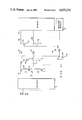
- FIG. 4 shows an embodiment of the semiconductor memory device according to the invention.
- reference numeral 11 designates a decoder which decodes an address input signal a 0 , a 0 , a 1 , a 1 , . . . to select one of the output lines R 1 , R 2 , . . .
- the output lines R 1 , R 2 , . . . are connected to the input terminal of respective buffer circuits A 1 , A 2 , . . .
- the output terminal of the buffer circuits A 1 , A 2 , . . . is connected to a main memory 18 through respective drive lines W 1 , W 2 , . . . thereof.
- the output lines R 1 , R 2 , . . . are also connected through respective enhancement type transistors 12 1 , 12 2 , . . . to the input terminal of a further buffer circuit A R1 and the drain of a depletion type MOS transistor 13.
- the source and gate of the transistor 13 are connected to a reference potential source VS (e.g., ground).
- the output terminal of the buffer circuit A R1 is connected through a buffer circuit A R2 to an auxiliary memory 19.
- Control circuits C 1 , C 2 , . . . on-off control the respective transistors 12 1 , 12 2 , . . .
- the control circuit C 1 includes depletion type MOS transistors 14 1 and 15 1 , an enhancement type MOS transistor 16 1 and a fuse element P 1 , consisting of polysilicon, for example.
- the transistors 15 1 and 16 1 form an inverter.
- the drain-source path of the depletion type MOS transistor 14 1 is connected at one terminal through the fuse element P 1 to a potential source VD and at the other terminal to the reference potential source VS. Its gate is also connected to the reference potential source VS.
- the inverter consisting of the transistors 15 1 and 16 1 is connected between the potential source VD and reference potential source VS. Its input terminal, i.e., the gate of the transistor 16 1 , is connected to the junction between the fuse element P 1 and transistor 14 1 .
- Its output terminal i.e., the junction between the transistors 15 1 and 16 1 , is connected to the gate of the transistor 12 1 .
- the control circuit C 2 and also the other control circuits (not shown) that are connected to their respective output lines have the same construction as the control circuit C 1 .
- the following description concerning the control circuit applies to each control circuit, but only the control circuit C 1 will be described for the sake of simplicity.
- the parts corresponding to those in the control circuit C 1 are designated by like reference numerals and symbols with a different suffix.
- the drive lines W 1 , W 2 , . . . are connected through respective transistors 17 1 , 17 2 , . . . to the reference potential source VS.
- the gate of the transistors 17 1 , 17 2 , . . . is connected to the output terminal of the buffer circuit A R1 .
- the control circuit C 1 has two different output levels depending upon whether the fuse element P 1 remains intact or is burned out.
- the transistor 12 1 is controlled according to the state of the fuse element P 1 . It is now assumed that the fuse element P 1 connected between the potential source VD and transistor 14 1 remains intact. In this case, the junction between the fuse element P 1 and transistor 14 1 is at the "1" level. Thus, the transistor 16 1 is "on", so that the inverter consisting of the transistors 15 1 and 16 1 , i.e., the control circuit C 1 , provides a "0" level output to hold the transistor 12 1 "off".
- the inverter i.e., the control circuit C 1
- the control circuit C 1 provides a "1" level output to turn on the transistor 12 1 .
- the output of the control circuit C 1 is at either one of the two levels depending upon whether the fuse element P 1 connected between the potential source VD and transistor 14 1 remains intact or it is burned out, and the transistor 12 1 is on-off controlled according to the state of the fuse element P 1 .
- the fuse elements P 1 , P 2 , . . . in the respective control circuits C 1 , C 2 , . . . connected between the potential source VD and the respective transistors 14 1 , 14 2 , . . . are not burned out but remain intact.
- the transistors 12 1 , 12 2 , . . . are thus "off", so that the outputs of the decoder are applied through the respective buffer circuits A 1 , A 2 , . . . to the main memory 18.
- the main memory 18 is thus selected and rendered operative. In this case, since the transistors 12 1 , 12 2 , . . .
- the junction B 1 between each of the transistors 12 1 , 12 2 , . . . and transistor 13 is held at the reference potential VS (i.e., at the "0" level) through the transistor 13.
- the output level of the buffer circuits A R1 and A R2 is thus "0" (i.e., level VS), and the auxiliary memory 19, which is not selected, remains inoperative.
- the fuse element P 1 in the circuit C 1 is burned out, for instance by irradiating it with a laser beam.
- the gate of the transistor 16 1 is held at the "0" level through the transistor 14 1 , thus keeping the transistor 16 1 "off".
- the gate of the transistor 12 1 is thus held at the source potential level VD (e.g., 5 volts) through the transistor 15 1 , thus keeping the transistor 12 1 "on”.
- the decoder output line R 1 is thus connected to the point B 1 .
- the point B 1 is also set to the "1" level by the transistor 12 1 .
- the buffer circuits A R1 and A R2 thus both provide a "1" level output.
- the auxiliary memory 19 is thus selected and rendered operative.
- the resistance of the transistor is set to a sufficiently high value to allow the point B 1 to go to the "1" level.
- the transistors 17 1 , 17 2 , . . . are turned on by the "1" level output of the buffer circuit A R1 , and thus, the main memory 18 is not selected.
- the auxiliary memory 19 can be substituted for the main memory 18 by burning out a single fuse element such as the fuse element P 1 in the control circuit C 1 , for instance by irradiating the same with a laser beam.
- FIG. 4 has a single auxiliary memory
- similar effects of the invention can also be obtained in cases where there are two auxiliary memories.
- the transistors 12 1 , 12 2 , . . . , transistor 13, circuits C 1 , C 2 , . . . , buffer circuits A R1 and A R2 and transistors 17 1 , 17 2 , . . . may be provided in duplicate.
- FIG. 5 shows a different example of the control circuit C 1 . While in the circuit C 1 shown in FIG. 4 the fuse element P 1 is adapted to be burned out with, for example, a laser beam, in the circuit of FIG. 5 a high resistance polysilicon element 21 is laser annealed, i.e., rendered in the low resistance state by irradiation with a laser beam, thereby causing a change of the output level of the circuit to "1".
- the high resistance polysilicon element 21 has one terminal connected through a depletion type MOS transistor 22 to the potential source VD, and the other terminal connected to the reference potential source VS.
- the gate of the transistor 22 is connected to the junction between the transistor 22 and high resistance polysilicon element 21.
- the gate of the transistor 22 is also connected to the gate of the transistor 16 1 .
- the circuit further includes an inverter, which consists of a depletion type MOS transistor 15 1 and an enhancement type MOS transistor 16 1 and is connected between the potential source VD and reference potential source VS.
- the output terminal of the inverter i.e., the junction between the MOS transistor 15 1 and 16 1 , is connected to the gate of the transistor 12 1 .
- the high resistance polysilicon element 21 remains intact unless the memory bit cells connected to the drive line W 1 of the main memory 18 include an error bit cell.
- the junction between the transistor 22 and the high resistance polysilicon element 21 is held at the "1" level.
- the transistor 16 1 is “on” to hold the gate of the transistor 12 1 at the "0" level, and hence, hold the transistor 12 1 "on”.
- the decoder output line R 1 is thus held apart from the point B 1 .
- the high resistance polysilicon 21 is changed to the low resistance state by laser annealing, for instance. In this state, the gate of the transistor 16 1 is held at the "0" level to hold the transistor 16 1 "off”.
- the gate potential on the transistor 12 1 is thus held at the "1" level through the transistor 15 1 , so that the transistor 12 1 is “off”.
- the auxiliary memory 19 is thus selected in this case in the manner as described before in connection with FIG. 4.
- FIG. 6 shows a modification of the circuit of FIG. 5 for reducing power consumption.
- the decoder output on the output line R 1 is fed to the gate of transistors 31 and 32 so that the circuit is only operated when the decoder output level becomes "1". More specifically, in the circuit of FIG. 6 the transistor 31 is connected between the potential source VD and transistor 15 1 while the transistor 32 is connected between the high resistance polysilicon element 21 and reference potential source VS. These transistors have their gates connected to the output line R 1 .
- This circuit is only rendered operative when the transistors 31 and 32 are turned on with a change of the decoder output appearing on the output line R 1 to the "1" level.
- the decoder output is "0"
- the transistors 31 and 32 are "off” so that the circuit is inoperative. In other words, unless the output line R 1 is selected, no current flows through the circuit. Thus, power consumption can be reduced.
- FIG. 7 shows a further modification of the control circuit C 1 in the memory device of FIG. 4.
- This circuit like the circuit of FIG. 6, includes two additional MOS transistors 41 and 42.
- the decoder output is applied to the gates of these transistors 41 and 42, and thereby the power consumption in the control circuit C 1 can be reduced.
- the additional MOS transistor 41 is connected between the transistor 14 1 and reference potential source VS, while the additional MOS transistor 42 is connected between the transistor 15 1 and potential source VD, with the gates of these MOS transistors 41 and 42 being connected to the output line R 1 of the decoder 11.
- the circuit is rendered operative only when the transistors 41 and 42 are turned on with a change of the output of the decoder 11 to the "1" level and is inoperative otherwise, i.e., when the decoder output is "0". In other words, unless the output line R 1 is selected, no current flows through the circuit, so that power consumption can be reduced.
- FIG. 8 shows a further modification of the control circuit C 1 shown in FIG. 4.
- a polysilicon fuse element P 1 is adapted to be burned out by Joule heat from a generated current.
- This circuit has an advantage over the circuit shown in FIG. 4, in which the fuse element P 1 is burned out by irradiation with a laser beam, in that a semiconductor memory device which uses this circuit can be sealed in a casing.
- This circuit uses two MOS transistors 51 and 52 in addition to the control circuit C 1 in the memory device of FIG. 4. These MOS transistors are connected in series between the polysilicon fuse element P 1 and reference potential source VS. The gate of the transistor 51 is connected to the output line R 1 of the decoder 11.
- a signal P for controlling the MOS transistor 52 is applied to the gate thereof.
- the address input signal to the decoder 11 is set to that locus which represents the address of the error bit cell.
- a "1" output is provided from the decoder to the output line R 1 to turn on the transistor 51.
- the signal P is set to "1" to turn on the transistor 52. Current is thus caused to flow through the fuse element P 1 and transistors 51 and 52.
- the fuse element P 1 is then burned out by Joule heat generated at this time.
- FIG. 9 shows a still further modification of the control circuit C 1 , the fuse element P 1 of which is again adapted to be burned out by a generated current.
- MOS transistors 61 to 67 are provided in addition to the circuit of FIG. 7.
- transistors 41 and 42 are provided for reducing power consumption.
- the transistor 41 in this circuit unlike the circuit of FIG. 7, is provided between the fuse element P 1 and transistor 14 1 . This, however, is a mere structural change, and there is no change in operation at all.
- the MOS transistor 61 which is a depletion type
- the MOS transistor 62 which is an enhancement type
- the MOS transistor 63 is connected between the transistor 62 and reference potential source VD.
- the input terminal of the inverter I 61 consisting of the transistors 61 and 62, i.e., the gate of the transistor 62, is connected to the output line R 1 of the decoder 11.
- a control signal P for on-off controlling the transistor 63 is applied to the gate thereof.
- the MOS transistor 65 which is a depletion type, and MOS transistor 64, which is an enhancement type, form another inverter I 65 connected between a high potential source VP and reference potential source VS.
- the MOS transistor 66 is connected between the input terminal of the inverter I 65 consisting of the transistors 64 and 65, i.e., the junction between the transistors 64 and 65, and the reference potential source VS.
- a complementary control signal P to the control signal P applied to the gate of the transistor 63 is applied to the gate of the transistor 66.
- the MOS transistor 67 is connected between the junction between the transistor 41 and fuse element P 1 and the reference potential source VS.
- the gate of the transistor 67 is connected to the input terminal of the second stage inverter I 65 , i.e., the junction between the transistors 64 and 65.
- the level of the high potential source VP may be set to approximately 15 volts. The use of such a high potential source allows a large current to burn out the fuse element P 1 even if the size of the transistor, through which the burn-out current flows, is small. Thus, it permits increasing the packing density of the device.
- the address input signal to the decoder 11 is set to select the output line R 1 like the example of FIG. 8.
- the transistor 62 is turned on.
- the signal P is set to "1" to turn on the transistor 63.
- the potential on the gate of the transistor 64 is thus changed to the "0" level to turn off the transistor 64.
- the transistor 66 remains “off” since the signal P is "0".
- the gate of the transistor 67 is thus raised to the high potential VP to turn on the transistor 67. Current is thus caused to flow through the transistor 67 into the fuse element P 1 , whereby the fuse element P 1 is burned out by Joule heat.
- the resistance of the transistor 67 at this point is very low since its gate is at the high potential VP. Thus, a large current can reliably burn out the fuse element P 1 even if the transistor 67 is small.
- the high potential source VP is used only when burning out the fuse, and after the burn-out operation the gate of the transistor 67 is brought to the "0" level to turn off the transistor 67. With the fuse element P 1 burned out, the gate of the transistor 16 1 is now at the reference potential to hold the transistor 16 1 "off". In this state, when the output line R 1 of the decoder 11 is selected, the output of the inverter consisting of the transistors 15 1 and 16 1 goes to the "1" level to turn on the transistor 12 1 . The auxiliary memory 19 is thus substituted for the main memory 18.
- FIG. 10 shows an example of the buffer circuit A 1 provided between the output line R 1 and drive line W 1 in the memory device of FIG. 4.
- the circuit has MOS transistors 71 to 78.
- the transistors 71 and 72 which are depletion type and enhancement type, respectively, are connected in series between the potential source VD and reference potential source VS to form an inverter I 71 .
- the input terminal of the inverter I 71 i.e., the gate of the transistor 72, is connected to the junction B 1 between the transistors 12 1 and 13 in the memory device of FIG. 4.
- the transistor 73 which is a depletion type, and transistors 74 and 75, which are enhancement type, are connected in series in the mentioned order between the potential source VD and reference potential source VS.
- the transistors 73 and 74 form an inverter I 73 .
- the transistors 76 to 78 are connected in series in the mentioned order between the potential source VD and reference potential source VS.
- the output terminal of the inverter consisting of the transistors 71 and 72 i.e., the junction between the transistors 71 and 72, is connected to the gate of each of the transistors 75 and 76.
- the gates of the transistors 74 and 77 are connected to the output line R 1 of the decoder 11.
- the output terminal of the inverter I 73 consisting of the transistors 73 and 74, i.e., the junction between the transistors 73 and 74, is connected to the gate of the transistor 78.
- the junction between the transistors 77 and 78 is connected to the drive line W 1 connected to the main memory 18.
- the inverter I 71 consisting of the transistors 71 and 72 provides a "1" output, that is, a "1" input is applied to the gate of each of the transistors 75 and 76 to hold these transistors 75 and 76 "on".
- the buffer circuit thus provides a signal at a level corresponding to the level of the output line R 1 to the drive line W 1 . If the level of the output line R 1 becomes "1", the transistors 74 and 73 are turned on.
- the output of the inverter I 73 consisting of the transistors 73 and 74 becomes “0" to turn off the transistor 78.
- a "1" level signal is thus provided from the junction between the transistors 77 and 78. If the level of the output line R 1 becomes “0”, the transistors 74 and 77 are both turned off. With the transistor 74 turned off, the output of the inverter I 73 consisting of the transistors 73 and 74 becomes “1” to turn on the transistor 78. A "0" level signal is thus provided from the junction between the transistors 77 and 78.
- the inverter I 71 consisting of the transistors 71 and 72 provides a "0" level output. That is, a "0" level input is applied to the gate of each of the transistors 75 and 76 to keep the transistors 75 and 76 “off".
- the buffer circuit A 1 thus provides a "0" level output irrespective of the level of the output line R 1 . More particularly, with the transistors 75 and 76 turned off, the buffer circuit A 1 provides a "0" level signal at all times and is not influenced by whether the level of the output line R 1 is "0" or "1".
- a transistor circuit for selecting the auxiliary memory is provided between the decoder and auxiliary memory and on-off controlled depending upon whether a single fuse element assembled in the control circuit is burned out or not or whether a high resistance polysilicon element assembled in the control circuit is rendered in a low resistance state or not.
- the operation of selecting the auxiliary memory can be readily accomplished with high reliability.
- FIG. 11 shows a different embodiment of the memory device according to the invention.
- control circuit C 1 includes a high resistance polysilicon element R P1 and a MOS transistor 111 1 having one terminal connected through the high resistance polysilicon element R P1 to a potential source VD and the other terminal connected to a reference potential terminal VS.
- MOS transistors 112 and 113 connected in series between the reference potential source VS and junction B 1 are used in lieu of the MOS transistor 12 1 in the embodiment of FIG. 4.
- this embodiment does not include the buffer circuits A R1 and A R2 as in the embodiment of FIG. 4. Instead, it uses an inverter I 114 , which has its input terminal connected to the junction B 1 and its output terminal connected to the gates of transistors 17 1 , 17 2 , . . . , and another inverter I 115 , which has its input terminal connected to the junction B 1 and its output terminal connected to auxiliary memory 19.
- the junction between the high resistance polysilicon element R P1 and transistor 111 1 is held at a "0" level so long as the high resistance polysilicon element R P1 remains as such, i.e., is in a high resistance state.
- the gate potential on the transistor 113 is at the "0" level so that the transistor 113 is "off”.
- the junction is at the "1" level.
- the gate potential on the transistor 113 is at the "1" level so that the transistor 113 is "on”.
- the memory bit cells connected to the drive line W 1 do not include any error bit cell.
- the high resistance polysilicon element R P1 is held as such, i.e., in the high resistance state.
- the control circuit C 1 provides a "0" level output so that the transistor 113 is “off”.
- the junction B 1 is thus held at the source potential VD through the transistor 114, that is, it is held at the "1" level.
- the output level of the inverter I 115 connected to the auxiliary memory 19 is thus "0", so that the auxiliary memory 19 is not selected.
- the control circuit C 1 provides a "1" level output to hold the transistor 113 "on".
- the output line R 1 of the decoder 11 becomes “1” level
- the gate potential level on the transistor 112 becomes “1” to turn on the transistor 112.
- the transistors 112 and 113 are both “on”, so that the level on the junction B 1 becomes “0".
- the inverter I 115 thus provides a "1" level output to select the auxiliary memory 19.
- the output of the inverter I 114 is also changed to "1" to turn on the transistors 17 1 , 17 2 , . . .
- the drive line W 1 is thus brought to the reference potential source level VS, thus the main memory 18 is not selected.
- FIG. 12 shows a modification of the control circuit C 1 in the memory device of FIG. 11.
- a polysilicon fuse element P is used in lieu of the high resistance polysilicon element R P1 in FIG. 11.
- the polysilicon fuse element P is connected at one terminal through a depletion type MOS transistor 116 to the potential source VD and at the other terminal to the reference potential source VS.
- the junction between the polysilicon fuse element P and transistor 116 is connected to the gate of the transistor 113 in the memory device of FIG. 11. In this circuit, so long as the polysilicon fuse element P is held without being burned out, the output level remains "0". On the other hand, when the fuse element P is burned out, it becomes "1".
- the polysilicon fuse element P may be burned out by irradiating it with a laser beam, for instance.
- FIG. 13 shows an example of the inverter I 115 in the memory device of FIG. 11.
- This circuit includes an inverter I 117 , which consists of a depletion type MOS transistor 117 and an enhancement type MOS transistor 118, these transistors being connected in series between the potential source VD and a reference potential source VS, and two series MOS transistors 119 and 120 connected in the mentioned order between the potential source VD and reference potential source VS.
- the input terminal of the inverter I 117 i.e., the gate of the transistor 118, and the gate of the transistor 120 connected to the reference potential source VS are both connected to the junction B 1 in the memory device of FIG. 11.
- the gate of the transistor 119 connected to the potential source VD is connected to the output terminal of the inverter I 117 , i.e., the junction between the transistors 117 and 118.
- the junction between the transistors 119 and 120 is connected to the auxiliary memory 19.
- FIG. 14 shows an example of the buffer circuit A 1 in the memory device of FIG. 11.
- This circuit reduces power consumption in addition to its buffer function. It includes an inverter I 121 , which consists of a depletion type MOS transistor 121, and an enhancement type MOS transistor 122, these transistors being connected in series between the potential source VD and reference potential source VS. It also includes transistors 123 to 125 connected in series in the mentioned order between the potential source VD and reference potential source VS. It further includes a MOS transistor 126 having one terminal connected through the inverter I 121 to the potential source VD and the other terminal connected to the reference potential source VS.
- the gate of the transistor 122 in the inverter I 121 and the gate of the second transistor 124 in the series MOS transistor circuit are connected to the output line R 1 .
- the gate of the third transistor 125 in the series MOS transistor circuit is connected to the output terminal of the inverter I 121 , i.e., the junction between the transistors 121 and 122.
- the transistors 126 and 123 are provided for reducing power consumption, and their gate is connected to the junction B 1 in the memory device of FIG. 11.
- the gate potential level on the transistors 123 and 126 is “1” so that these transistors 123 and 126 are “on”.
- the output signal of the buffer circuit A 1 is thus at a level corresponding to the input signal level.
- the gate potential level on the transistor 122 in the inverter I 121 and the second transistor 124 in the series MOS transistor circuit becomes "1" to turn on the transistors 122 and 124.
- the buffer circuit A 1 provides an output signal at the same level as the input signal level.
- the output line R 1 is not selected, i.e., when the level thereof is changed to "0"
- the gate level of the transistors 122 and 124 becomes “0” to turn off these transistors.
- the output level of the inverter I 121 becomes "1" to turn on the transistor 125.
- the buffer circuit A 1 thus provides an output signal at the same level as the input signal level of "0". As has been shown, the output level of the buffer circuit A 1 corresponds to the input level while the transistors 123 and 126 are "on”.
- the auxiliary memory 19 When the auxiliary memory 19 is in the selected state, i.e., when the potential level at the junction B 1 in the memory device of FIG. 11 is "0", the gate potential level on the transistors 123 and 126 is “0" so that these transistors 123 and 126 are “off". In this case, the output level of the buffer circuit A 1 is "0" irrespective of the input level.
- the inverter I 121 provides a "1" level output irrespective of the level of the output line R 1 so that the transistor 125 is held “on”. Therefore, the junction between the transistors 124 and 125 is kept apart from the potential VD irrespective of the level of the output line R 1 . The output level of the buffer circuit A 1 is thus held at "0" irrespective of the input level.
- the buffer circuit A 1 described above functions to inhibit the selection of the level of the drive line of the main memory 18, while the transistors 123 and 126 function to reduce power consumption while the main memory 18 is in the non-selected state. Where this buffer circuit is used, the transistors 17 1 , 17 2 , . . . in the memory device of FIG. 11 are unnecessary.
- FIG. 15 shows a modification of the circuit consisting of the control circuit C 1 and transistors 112 1 and 113 1 in the memory device of FIG. 11.
- a high resistance polysilicon element C 1 and a depletion type MOS transistor 127 having one terminal connected to the potential source VD and the other terminal connected to the reference potential source VS are used in lieu of the control circuit C 1 in the memory device of FIG. 11.
- the circuit further includes an inverter I 128 , which consists of a depletion type MOS transistor 128 and an enhancement type MOS transistor 124, these transistors being connected in series between the potential source VD and reference potential source VS, and another inverter I 120 , which consists of a depletion type MOS transistor 130 and an enhancement type MOS transistor 131, these transistors being connected in series between the potential source VD and reference potential source VS. It further includes a MOS transistor 132, which has one terminal connected to the reference potential source VS, the other terminal connected to the junction B 1 shown in FIG. 11 and the gate connected to the output terminal of the inverter I 128 , i.e., the junction between the transistors 128 and 129.
- MOS transistor 132 which has one terminal connected to the reference potential source VS, the other terminal connected to the output terminal of the inverter I 128 and the gate connected to the output terminal of the inverter I 130 , i.e., the junction between the transistors 130 and 131.
- the circuit consisting of the inverters I 128 and I 130 and MOS transistors 132 and 133 has the same function as the circuit consisting of the transistors 112 and 113 in the memory device of FIG. 11.
- the gate of the inverter I 128 is connected to the output terminal of the control circuit C 1 .
- the gate of the transistor 131 of the inverter I 130 is connected to the output line R 1 of the decoder 11 of the memory device of FIG. 11.
- the high resistance polysilicon element R P in the control circuit C 1 is kept in this state.
- the gate potential on the transistor 129 is thus “1” so that this transistor is “on”.
- the transistor 132 which is connected between the potential source VS and junction B 1 is thus "off”. Therefore, when the output line R 1 of the decoder 11 is selected in this state, the main memory 18 is selected while the auxiliary memory 19 is not selected. If the memory bit cells connected to the drive line W 1 include an error bit cell, the high resistance polysilicon element R P is changed to the low resistance state by laser annealing.
- the gate potential level on the transistor 129 is changed to "0" so that the transistor 129 is turned off.
- the output line R 1 is selected to the "1" level
- the transistor 131 of the inverter I 130 is turned on.
- the output level of the inverter I 130 becomes “0” to turn off the transistor 133.
- the gate potential level on the transistor 132 thus becomes “1” so that this transistor is turned off.
- a "0" level output is provided from the junction B 1 , so that the auxiliary memory 19 is not selected.
- FIG. 16 shows a further modification of the circuit consisting of the control circuit C 1 and transistors 112 1 and 113 1 in the memory device of FIG. 11.
- a high resistance polysilicon element R P and a depletion type MOS transistor 134 having one terminal connected through the high resistance polysilicon element R P to the potential source VD and the other terminal connected to the reference potential source VS and used in lieu of the control circuit C 1 in the memory device of FIG. 11.
- the circuit further includes a MOS transistor 135 connected between the high resistance polysilicon element R P and potential source VD.
- the gate of the transistor 135 is connected to the output line R 1 of the decoder 11.
- the junction between the high resistance polysilicon element R P and transistor 134 is connected to the gate of the MOS transistor 136.
- the transistor 136 is connected at one terminal to the junction B 1 and at the other terminal to the reference potential source VS.
- the high resistance polysilicon element R P remains in the high resistance state.
- the gate potential level on the transistor 136 is thus "0" so that this transistor 136 is "off".
- the drive line W 1 i.e., the main memory 18 is selected while the auxiliary memory 19 is not selected.
- the high resistance polysilicon element R P is thus rendered in the low resistance state by laser annealing. In this state, the transistor 136 operates depending upon the operation of the transistor 135.
- FIG. 17 shows a further embodiment of the memory device according to the invention.
- like parts to those in the preceding embodiments of FIGS. 4 and 11 are designated by like reference numerals and symbols.
- a buffer circuit A 3 is used in lieu of the circuit consisting of the transistors 112 1 and 113 1 in the preceding embodiment of FIG. 11, while the same circuit as the control circuit C 1 in the embodiment of FIG. 11 is used.
- the buffer circuit A 3 has its input terminals connected to the output line R 1 of the decoder 11 and the output terminal of the control circuit C 1 respectively. Its output terminal is connected through buffer circuit A 4 to auxiliary memory 19, and also connected to the gate of each of transistors 17 1 , 17 2 , . . .
- the junction between the output of the buffer circuit A 3 and the input terminal of each of the buffer circuits A 4 and A 5 is indicated at B 2 .
- the main memory 18 is thus selected.
- the control circuit C 1 If there is an error bit cell connected to the drive line W 1 , in which case the high resistance polysilicon element R P is rendered in the low resistance state, the control circuit C 1 provides a "1" level output. In this case, the buffer circuit A 3 changes the level on the junction B 2 according to the level on the output line R 1 of the decoder 11 to access the auxiliary memory 19.
- FIG. 18 shows an example of the buffer circuit A 3 .
- This circuit includes an inverter I 211 consisting of a depletion type MOS transistor 211 and an enhancement type MOS transistor 212, these transistors being connected in series between the potential source VD and reference potential source VS, and MOS transistors 213 to 216 connected in series in the mentioned order between the potential source VD and reference potential source VS from the side of the potential source VD.
- the gate of the transistor 212 in the inverter I 211 and the gate of the second transistor 214 in the series MOS transistor circuit are connected to the output line R 1 of the decoder 11.
- the gate of each of the transistors 213 and 215 in the series MOS transistor circuit is connected to the output terminal E of the control circuit C 1 .
- the output terminal of the inverter I 211 i.e., the junction between the transistors 211 and 212, is connected to the gate of the fourth transistor 216 in the series MOS transistor circuit.
- the junction between the transistors 124 and 125 of the series MOS transistor circuit constitutes the output terminal of the buffer circuit A 3 .
- the output level of the control circuit C 1 is "0"
- the gate level on the first and third transistors 213 and 215 of the series MOS transistor circuit is "0" to hold these transistors 213 and 215 "off".
- the level of the junction B 2 is not affected at all by the level of the output line R 1 of the decoder 11.
- the output level of the control circuit C 1 is "1"
- the gate level on the first and third transistors 213 and 215 in the series MOS transistor circuit is "1" to hold these transistors 213 and 215 "on”.
- the level of the output line R 1 of the decoder 11 is changed according to the level of the junction B 2 . More specifically, when the output line R 1 is selected so that its level becomes “1”, the transistor 212 in the inverter I 211 and the second transistor 214 of the series MOS transistor circuit are turned on. With the transistor 212 turned on, the output level of the inverter I 211 becomes “0" to turn off the transistor 216. The output level of the buffer circuit A 3 thus becomes “1”. A “1" level output is thus provided from the junction B 2 . This "1" level signal is fed through the buffer device A 4 in the memory device of FIG. 17 to the auxiliary memory 19. The auxiliary memory 19 is thus selected and rendered operative. The "1" level signal from the buffer circuit A 3 is also fed through the buffer circuit A 5 to the gate of each of the transistors 17 1 , 17 2 , . . . to turn on these transistors.
- FIG. 19 shows an example of the buffer circuit A 2 in the memory device of FIG. 17.
- This circuit includes an inverter I 217 consisting of a depletion type MOS transistor 217 and an enhancement type MOS transistor 218, these transistors being connected in series between the potential source VD and reference potential source VS. It also includes another inverter I 219 consisting of a depletion type MOS transistor 219 and an enhancement type MOS transistor 220, these transistors being connected in series between the potential source VD and reference potential source VS. It further includes a MOS transistor 221 connected between the inverter I 219 and reference potential source VS and transistors 222 to 224 connected in series in the given order between the potential source VD and reference potential source VS.
- the gate of the transistor 218 in the inverter I 217 is connected to the junction B 2 in the memory device of FIG. 17.
- the gate of the transistor 220 in the inverter I 219 and the gate of the second transistor 223 in the series MOS transistor are connected to the output line R 1 of the decoder 11.
- the gate of the transistor 221 and the gate of the first transistor 222 in the series MOS transistor circuit are connected to the output terminal of the inverter I 217 , i.e., the junction between the transistors 217 and 218.
- the gate of the third transistor 224 in the series MOS transistor circuit is connected to the output terminal of the inverter I 219 , i.e., the junction between the transistors 219 and 220.
- the junction between the transistors 223 and 224 constitutes the output terminal of the buffer circuit A 2 .
- the selection of the output line R 1 of the decoder 11 to the "1" level sets the junction B 2 to the "0" level.
- the transistor 218 of the inverter I 217 is turned off to change the output level of the inverter I 217 to "1".
- the gate potential level on the transistors 221 and 222 thus becomes “1” to turn on these transistors 221 and 222.
- the transistors 220 and 223 are turned on.
- the buffer circuit A 2 thus provides an output at the same level as the input level, i.e., "1".
- the main memory 18 is thus selected and rendered operative. If the memory bit cells connected to the drive line W 1 include an error bit cell, with the selection of the output line R 1 to the "1" level the level of the junction B 2 becomes “1". As a result, the transistor 218 in the inverter I 217 is turned on. The output level of the inverter I 217 thus becomes "0" to turn off the transistors 221 and 222. In this case, the buffer circuit A 2 provides a "0" level output so that the main memory 19 is not selected and rendered inoperative. In this example, the transistors 221 and 222 are used in lieu of the transistor 17 1 in the embodiment of FIG. 17. Where this buffer circuit is used, the transistor 17 1 in the memory device of FIG. 17 is thus unnecessary.
- a transistor circuit is provided between the decoder and auxiliary memory and is on-off controlled according to whether or not a single polysilicon fuse element incorporated in its on-off control circuit is burned out or whether a single high resistance polysilicon element in the on-off control circuit is changed to the low resistance state.
- the auxiliary memory can thus be readily and reliably selected and rendered operative.
- FIGS. 20A and 20B show a further embodiment of the memory device according to the invention.
- the invention is applied to both row and column line circuits.
- parts similar to those in the preceding embodiments are designated by like reference numerals and symbols.
- a column decoder 311 decodes address input signals a 0 , a 0 , a 1 , a 1 , . . . to select one of its output lines R 11 , R 12 , . . .
- a row decoder 312 similarly decodes address input signals A 0 , A 0 , A 1 , A 1 , . . . to select one of its output lines R 21 , R 22 , . . .
- the output lines R 11 , R 12 , . . . of the column decoder 311 are connected through respective buffer circuits A 11 , A 12 , . . . to corresponding column selecting lines CS 1 , CS 2 , . . .
- the column selecting circuit 313 is connected to column lines C 1 , C 2 , . . . which are common to a main memory 18 and an auxiliary memory 19.
- the output lines R 21 , R 22 , . . . of the row decoder 312 are connected through respective buffer circuits A 21 , A 22 , . . . to corresponding drive lines R L1 , R L2 , . . . of the main memory 18.
- the row decoder 312 are each provided with a transistor circuit consisting of transistors generally designated at 112 and 113. These output lines are also provided with respective control circuits C 11 , C 12 , . . . , each of which includes a high resistance polysilicon element generally designated at R P for controlling the transistor 113 and a depletion type MOS transistor generally designated at 111.
- the construction of the transistor circuits and control circuits C 11 , C 12 , . . . is substantially the same as in the embodiment of FIG. 11, so the component elements are designated by the same reference numerals and symbols with a suffix.
- the output lines leading from the respective transistors 112 11 , 112 13 , . . . are commonly connected via a line Y 1 to an auxiliary memory selecting circuit 314.
- the output lines leading from the transistors 112 12 , 112 14 , . . . are commonly connected via a line Y 2 to the auxiliary memory selecting circuit 314.
- the output lines leading from the transistors 112 21 , 112 23 , . . . are commonly connected via a line X 1 to the auxiliary memory selecting circuit 314.
- the output lines leading from the transistors 112 22 , 112 24 , . . . are connected via a line X 2 to the auxiliary memory selecting circuit 314.
- the auxiliary memory selecting circuit 314 has its output terminal connected to a drive line R L0 of the auxiliary memory 19.
- the drive lines R L1 , R L2 , . . . of the main memory 18 are connected through respective MOS transistors 315 1 , 315 2 , . . . to a reference potential source VS.
- the gate of each of the transistors 315 1 , 315 2 , . . . is connected to the output terminal of the auxiliary memory selecting circuit 314.
- the column decoder 311 can select one of the column lines CS 1 , CS 2 , . . . and set it to the "1" level according to the address input signals a 0 , a 0 , a 1 , a 1 , . . .
- the column selecting circuit 313 selects the corresponding column line. For example, when the column selecting line CS 1 is set to the "1" level, the corresponding column line C 1 is selected. Data is read out from a memory bit cell at the intersection between the selected drive and column lines.
- the memory bit cell selected by the column line C 1 and drive line R L2 is an error bit cell.
- the high resistance polysilicon elements R P11 , and R P23 in the respective control circuits C 11 and C 23 are changed a low resistance state by laser annealing, for instance.
- the gate potential on the transistors 113 11 and 113 23 is changed to "1" so that these transistors are turned on.
- the level of the lines X 1 and Y 1 is determined by the state of the transistors 112 11 , 112 23 ; the level of the line Y 1 is “0” if the transistor 112 11 is “on” and “1” if the transistor 112 11 is “off”, and the level on the line X 1 is “0” if the transistor 112 23 is “on” and “1” if the transistor 112 23 is “off”. It is now assumed that the column line C 1 and drive line R L2 are selected and set to the "1" level by the respective column and row decoders 311 and 312 with the high resistance polysilicon elements R P11 and R P23 in the low resistance state.
- the transistors 112 11 and 112 23 are both turned on to set the lines Y 1 and X 1 to the "0" level. With the lines X 1 and Y 1 both set to the "0" level, the auxiliary memory selecting circuit 314 provides a "1" level signal to the output line R L0 . The auxiliary memory 19 is thus selected and rendered operative.
- the "1" level output of the auxiliary memory selecting circuit 314 is also applied to the gate of the transistors 315 1 , 315 2 , . . .
- the main memory 18 is not selected and rendered inoperative when the auxiliary memory 19 is selected and rendered operative.
- the high resistance polysilicon elements corresponding to that error bit cell among those R P12 , R P14 , . . . and R P22 , R P24 , . . . connected to the lines Y 2 and X 2 are rendered in the low resistance state.
- the level of both the lines X 2 and Y 2 becomes "0".
- the output level of the auxiliary memory selecting circuit 314 thus becomes "1" to select the auxiliary memory 19.
- the auxiliary memory selecting circuit 314 provides a "1" level signal to select the auxiliary memory 19 only when the level of both the lines X 1 and Y 1 or the level of both the lines X 2 and Y 2 becomes "0".
- the memory bit cells of the auxiliary memory 19 are arranged such that the row lines thereof can be selected by the auxiliary memory selecting circuit 314.
- FIG. 21 shows an example of the auxiliary memory selecting circuit 314 in the memory device of FIGS. 20A and 20B.
- This circuit includes a depletion type MOS transistor 431 having one terminal connected to potential source VD, MOS transistors 432 and 433 each having one terminal connected through the transistor 431 to the potential source VD and the other terminal connected to the reference potential source VS, a depletion type MOS transistor 435 having one terminal connected to the potential source VD, and MOS transistors 434 and 436 each having one terminal connected through the transistor 435 to the potential source VD and the other terminal connected to the reference potential source VS.
- the transistors 431, 432 and 433 constitute a NOR gate.
- the transistors 434, 435 and 436 constitute another NOR gate.
- the transistors 437, 438 and 439 constitute a still another NOR gate.
- the gate of the transistor 432 is connected to the signal line X 1 in the memory device of FIG. 20.
- the gate of the transistor 433 is connected to the signal line Y 1 .
- the gate of the transistor 438 is connected to the signal line X 2 .
- the gate of the transistor 439 is connected to the signal line Y 2 .
- the gate of the transistor is connected to the junction between the transistors 432 and 433.
- the gate of the transistor 436 is connected to the junction between the transistors 438 and 439.
- the gate of the transistor 441 is connected to the junction between the transistors 435 and each of the transistors 434 and 436.
- the gate of the transistor 442 is connected to the output terminal of the inverter I 440 , i.e., the junction between the transistors 440 and 441.
- the junction between the transistors 442 and 443 constitutes the output terminal of this auxiliary memory selecting circuit 314, and is connected to the drive line R L0 .
- the junction between the transistor 435 and each of the transistors 434 and 436 constitutes a node N.
- the level of one or both of the signal lines X 1 and Y 1 is “1". Also, the level of one or both of the signal lines X 2 and Y 2 is “1".
- the gate of the transistors 434 and 436 is thus at the “0" level so that these transistors are “off”.
- the gate of the transistors 441 and 443, i.e., the node N is thus at the "1" level so that these transistors are "on”.
- the gate level of the transistor 442 is "0" to render the transistor 442 turned off.
- the output of the auxiliary memory selecting circuit 314 is at the "0" level to keep the drive line R L0 at the "0" level.
- the auxiliary memory 19 is thus not selected and rendered inoperative.
- FIG. 22 shows a modification of the circuit consisting of the high resistance polysilicon element R P and transistors 111, 112 and 113 in the memory device of FIG. 22.
- a single high resistance polysilicon element 451 is used instead of the circuit in the construction of FIG. 22 noted above.
- the high resistance polysilicon element 451 is connected at one terminal to the output line R 11 of the decoder 311 and at the other terminal to a signal line X 1 complementary to the signal line X 1 . If the memory bit cells connected to the column line C 1 of the main memory 18 include an error bit cell, the high resistance polysilicon element 451 is changed to the low resistance state by laser annealing, for example.
- FIG. 23 shows an example of the auxiliary memory selecting circuit 114 in the memory device of FIGS. 20A and 20B incorporating the construction of FIG. 22.
- the circuit includes a NAND gate I 461 having a depletion type MOS transistor 461 and enhancement type MOS transistors 462 and 463, these transistors being connected in series between the potential source VD and reference potential source VS. It also includes another NAND gate I 464 having a depletion type MOS transistor 464 and enhancement type MOS transistors 465 and 466, these transistors being connected in series between the potential source VD and reference potential source VS. It further includes a third NAND gate I 467 having a depletion type MOS transistor 467 and enhancement type MOS transistors 468 and 469, these transistors being connected in series between the potential source VD and reference potential source VS.
- inverter I 470 having a depletion type MOS transistor 470 and an enhancement type MOS transistor 471, these transistors being connected in series between the potential source VD and reference potential source VS. It further includes two MOS transistors 472 and 473 connected in series between the potential source VD and reference potential source VS.
- the transistors 462, 463, 465 and 466 have their gates respectively connected to signal lines X 1 , Y 1 , X 2 and Y 2 .
- the gate of the transistor 468 is connected to the output terminal of the NAND gate I 461 , i.e., the junction between the transistors 461 and 462.
- the gate of the transistor 469 is connected to the output terminal of the NAND gate I 464 , i.e., the junction between the transistors 464 and 465.
- the gate of the transistor 471 is connected to the output terminal of the NAND gate I 467 , i.e., the junction between the transistors 467 and 468.
- the gate of the transistor 472 is connected to the output terminal of the NAND gate I 467 .
- the gate of the transistor 473 is connected to the output terminal of the inverter I 479 , i.e., the junction between the transistors 470 and 471.
- the junction between the transistors 472 and 473 constitutes the output terminal of this auxiliary memory selecting circuit 314.
- FIG. 24 shows an example of the buffer circuit A 21 in the memory device of FIG. 20.
- the circuit includes a NAND gate I 481 having a depletion type MOS transistor 481 and enhancement type MOS transistors 482 and 483, these transistors being connected in series in the mentioned order between the potential source VD and reference potential source VS from the side of the potential source VD. It also includes MOS transistors 484 to 486 connected in series between the potential source VD and reference potential source VS. The gate of each of the transistors 482 and 485 is connected to the output line R 21 .
- the output terminal of the NAND gate I 481 i.e., the junction between the transistors 481 and 482, is connected to the gate of the transistor 486.
- each of the transistors 483 and 484 is connected to the node N in the circuit of FIG. 21.
- the junction between the transistors 485 and 486 constitutes the output terminal of this buffer circuit A 21 , and is connected to the drive line R L1 .
- the buffer circuit A 21 provides a "1" level output if the level of the output line R 21 is “1", while it provides a "0" level output if the output line level is "0".
- the transistors 483 and 484 are turned on.
- the transistors 482 and 485 are turned on. With the transistor 482 turned on, the gate level of the transistor 486 becomes “0” to turn off the transistor 486.
- the output level of the buffer circuit A 21 thus becomes “1”.
- the transistors 482 and 485 are turned off. With the transistor 482 turned off, the gate level of the transistor 486 becomes “1” to turn on the transistor 486.
- the output level of the buffer circuit A 21 thus becomes “0".
- FIGS. 25, 26 and 27 show circuits which use a polysilicon fuse element which can be used in place of the high resistance polysilicon element R P in the memory device of FIGS. 20A and 20B.
- a fuse element is connected at one terminal to the reference potential source VS and at the other terminal through a depletion type MOS transistor 492 to the potential source VD.
- the junction between the fuse element 491 and transistor 492 constitutes the output terminal of this circuit. If the memory bit cells connected to the column line C 1 of the main memory 18 include an error bit cell, the fuse element 491 is burned out by irradiation thereof with a laser beam, for instance. With the fuse element 491 burned out, a "1" level output is provided.
- a fuse element 495 is connected at one terminal through a depletion type MOS transistor 494 to the potential source VD.
- the other terminal of the fuse element 495 is connected to the reference potential source VS through an enhancement type MOS transistor 493-1 and a depletion type MOS transistor 493-2 parallel connected each other.
- a pulse P is applied to the gate of the transistor 494.
- the gate of the transistor 493-1 is connected to the output line R 11 of the decoder 311.
- the gate of the transistor 493-2 is connected to the potential source VD. If the bit memory cells connected to the column line C 1 include an error bit cell, the fuse element 495 is burned out. It is burned out when address input signals designating the address of the error bit cell are generated.
- the transistor 493 is turned on.
- the pulse signal P 1 is set to "1", thus turning on the transistor 494.
- a large current is thus caused to flow through the fuse element 495 and it is burned out by Joule heat at this time.
- a "1" level signal is provided.
- a "0" level signal is provided through the transistor 493-2.
- a polysilicon fuse element 497 is connected at one terminal to a high potential source VP and at the other terminal through a depletion type MOS transistor 496 to the reference potential source VS.
- the junction between the fuse element 497 and transistor 496 is connected through an inverter 498 to the output terminal.
- the gate of the transistor 496 is connected to the output line R 11 of the decoder 311. If the memory bit cells connected to the column line C 1 of the main memory 18 include an error bit cell, the fuse element 497 is burned out. This is done when address input signals designating the error bit cell are input. To be more specific, when these address input signals are input, the transistor 496 is turned on.
- the voltage of the potential source VP is made about 15 V to cause a large current to flow through the fuse element 497, whereby the fuse element 497 is burned out.
- the voltage of the potential source VP is returned to the potential VD and the input level applied to the inverter 498 is "0" so that the output level thereof is "0".
- a transistor circuit is provided between the column decoder and auxiliary memory and is on-off controlled depending upon whether a single polysilicon fuse element incorporated in the control circuit is burned out or not or a single high resistance polysilicon element in the control circuit is changed to the low resistance state or not.
- a similar transistor circuit is provided between the row decoder and auxiliary memory and is similarly on-off controlled.
- the auxiliary memory can be readily and reliably selected and rendered operative.
- the invention it is possible to provide a semiconductor memory device with which the auxiliary memory can be easily and simply accessed, and which improves both the reliability and the probability of access to the auxiliary memory.
Landscapes
- Static Random-Access Memory (AREA)
- Dram (AREA)
- Techniques For Improving Reliability Of Storages (AREA)
- Read Only Memory (AREA)
- For Increasing The Reliability Of Semiconductor Memories (AREA)
Applications Claiming Priority (2)
| Application Number | Priority Date | Filing Date | Title |
|---|---|---|---|
| JP57047723A JPS58164099A (ja) | 1982-03-25 | 1982-03-25 | 半導体メモリ− |
| JP57-47723 | 1982-03-25 |
Publications (1)
| Publication Number | Publication Date |
|---|---|
| US4635232A true US4635232A (en) | 1987-01-06 |
Family
ID=12783238
Family Applications (1)
| Application Number | Title | Priority Date | Filing Date |
|---|---|---|---|
| US06/477,880 Expired - Lifetime US4635232A (en) | 1982-03-25 | 1983-03-23 | Semiconductor memory device |
Country Status (4)
| Country | Link |
|---|---|
| US (1) | US4635232A (de) |
| EP (1) | EP0090332B1 (de) |
| JP (1) | JPS58164099A (de) |
| DE (1) | DE3382252D1 (de) |
Cited By (12)
| Publication number | Priority date | Publication date | Assignee | Title |
|---|---|---|---|---|
| US4783781A (en) * | 1985-07-12 | 1988-11-08 | Fujitsu Limited | Semiconductor memory device having redundancy configuration with read circuit for defective memory address |
| US4839864A (en) * | 1987-03-09 | 1989-06-13 | Mitsubishi Denki Kabushiki Kaisha | Semiconductor memory device comprising programmable redundancy circuit |
| US4855621A (en) * | 1987-03-16 | 1989-08-08 | Siemens Aktiengesellschaft | Multi-stage, integrated decoder device having redundancy test enable |
| US4858192A (en) * | 1987-07-29 | 1989-08-15 | Kabushiki Kaisha Toshiba | Semiconductor memory device with redundancy circuit |
| US4996670A (en) * | 1989-09-28 | 1991-02-26 | International Business Machines Corporation | Zero standby power, radiation hardened, memory redundancy circuit |
| US5022002A (en) * | 1987-07-14 | 1991-06-04 | Kabushiki Kaisha Toshiba | Programmable ROM having a reduced number of power source terminals |
| US5173905A (en) * | 1990-03-29 | 1992-12-22 | Micron Technology, Inc. | Parity and error correction coding on integrated circuit addresses |
| US5359563A (en) * | 1991-03-29 | 1994-10-25 | International Business Machines Corporation | Memory system with adaptable redundancy |
| US5428572A (en) * | 1990-04-23 | 1995-06-27 | Kabushiki Kaisha Toshiba | Program element for use in redundancy technique for semiconductor memory device |
| US5495445A (en) * | 1994-05-31 | 1996-02-27 | Townsend And Townsend And Crew | Redundancy scheme for memory circuits |
| US5581513A (en) * | 1995-04-19 | 1996-12-03 | Cirrus Logic, Inc. | Continuous page random access memory and systems and methods using the same |
| US5737511A (en) * | 1996-06-13 | 1998-04-07 | United Microelectronics Corporation | Method of reducing chip size by modifying main wordline repair structure |
Families Citing this family (6)
| Publication number | Priority date | Publication date | Assignee | Title |
|---|---|---|---|---|
| JPS60191500A (ja) * | 1984-03-08 | 1985-09-28 | Sharp Corp | 冗長回路 |
| JPS60195797A (ja) * | 1984-03-16 | 1985-10-04 | Mitsubishi Electric Corp | 半導体記憶装置の冗長回路 |
| JPS60201598A (ja) * | 1984-03-23 | 1985-10-12 | Fujitsu Ltd | 半導体集積回路 |
| US4654830A (en) * | 1984-11-27 | 1987-03-31 | Monolithic Memories, Inc. | Method and structure for disabling and replacing defective memory in a PROM |
| FR2576132B1 (fr) * | 1985-01-15 | 1990-06-29 | Eurotechnique Sa | Memoire en circuit integre |
| US5635854A (en) * | 1994-05-24 | 1997-06-03 | Philips Electronics North America Corporation | Programmable logic integrated circuit including verify circuitry for classifying fuse link states as validly closed, validly open or invalid |
Citations (4)
| Publication number | Priority date | Publication date | Assignee | Title |
|---|---|---|---|---|
| US4365319A (en) * | 1979-11-13 | 1982-12-21 | Fujitsu Limited | Semiconductor memory device |
| US4392211A (en) * | 1979-06-25 | 1983-07-05 | Fujitsu Limited | Semiconductor memory device technical field |
| US4485459A (en) * | 1982-09-20 | 1984-11-27 | Fairchild Camera & Instrument Corp. | Redundant columns for byte wide memories |
| US4538245A (en) * | 1982-04-12 | 1985-08-27 | Seeq Technology, Inc. | Enabling circuit for redundant word lines in a semiconductor memory array |
Family Cites Families (4)
| Publication number | Priority date | Publication date | Assignee | Title |
|---|---|---|---|---|
| US3758761A (en) * | 1971-08-17 | 1973-09-11 | Texas Instruments Inc | Self-interconnecting/self-repairable electronic systems on a slice |
| US3940740A (en) * | 1973-06-27 | 1976-02-24 | Actron Industries, Inc. | Method for providing reconfigurable microelectronic circuit devices and products produced thereby |
| JPS5685934A (en) * | 1979-12-14 | 1981-07-13 | Nippon Telegr & Teleph Corp <Ntt> | Control signal generating circuit |
| US4346459A (en) * | 1980-06-30 | 1982-08-24 | Inmos Corporation | Redundancy scheme for an MOS memory |
-
1982
- 1982-03-25 JP JP57047723A patent/JPS58164099A/ja active Pending
-
1983
- 1983-03-22 DE DE8383102837T patent/DE3382252D1/de not_active Expired - Lifetime
- 1983-03-22 EP EP83102837A patent/EP0090332B1/de not_active Expired
- 1983-03-23 US US06/477,880 patent/US4635232A/en not_active Expired - Lifetime
Patent Citations (4)
| Publication number | Priority date | Publication date | Assignee | Title |
|---|---|---|---|---|
| US4392211A (en) * | 1979-06-25 | 1983-07-05 | Fujitsu Limited | Semiconductor memory device technical field |
| US4365319A (en) * | 1979-11-13 | 1982-12-21 | Fujitsu Limited | Semiconductor memory device |
| US4538245A (en) * | 1982-04-12 | 1985-08-27 | Seeq Technology, Inc. | Enabling circuit for redundant word lines in a semiconductor memory array |
| US4485459A (en) * | 1982-09-20 | 1984-11-27 | Fairchild Camera & Instrument Corp. | Redundant columns for byte wide memories |
Non-Patent Citations (2)
| Title |
|---|
| Kokkonen et al., "Redundancy Techniques for Fast Static RAMs", ISSCC Digest of Technical Papers, pp. 80-81, Feb. 18, 1981. |
| Kokkonen et al., Redundancy Techniques for Fast Static RAMs , ISSCC Digest of Technical Papers, pp. 80 81, Feb. 18, 1981. * |
Cited By (13)
| Publication number | Priority date | Publication date | Assignee | Title |
|---|---|---|---|---|
| US4783781A (en) * | 1985-07-12 | 1988-11-08 | Fujitsu Limited | Semiconductor memory device having redundancy configuration with read circuit for defective memory address |
| US4839864A (en) * | 1987-03-09 | 1989-06-13 | Mitsubishi Denki Kabushiki Kaisha | Semiconductor memory device comprising programmable redundancy circuit |
| US4855621A (en) * | 1987-03-16 | 1989-08-08 | Siemens Aktiengesellschaft | Multi-stage, integrated decoder device having redundancy test enable |
| US5022002A (en) * | 1987-07-14 | 1991-06-04 | Kabushiki Kaisha Toshiba | Programmable ROM having a reduced number of power source terminals |
| US4858192A (en) * | 1987-07-29 | 1989-08-15 | Kabushiki Kaisha Toshiba | Semiconductor memory device with redundancy circuit |
| US4996670A (en) * | 1989-09-28 | 1991-02-26 | International Business Machines Corporation | Zero standby power, radiation hardened, memory redundancy circuit |
| US5173905A (en) * | 1990-03-29 | 1992-12-22 | Micron Technology, Inc. | Parity and error correction coding on integrated circuit addresses |
| US5428572A (en) * | 1990-04-23 | 1995-06-27 | Kabushiki Kaisha Toshiba | Program element for use in redundancy technique for semiconductor memory device |
| US5359563A (en) * | 1991-03-29 | 1994-10-25 | International Business Machines Corporation | Memory system with adaptable redundancy |
| US5495445A (en) * | 1994-05-31 | 1996-02-27 | Townsend And Townsend And Crew | Redundancy scheme for memory circuits |
| US5572471A (en) * | 1994-05-31 | 1996-11-05 | Townsend And Townsend Khourie And Crew | Redundancy scheme for memory circuits |
| US5581513A (en) * | 1995-04-19 | 1996-12-03 | Cirrus Logic, Inc. | Continuous page random access memory and systems and methods using the same |
| US5737511A (en) * | 1996-06-13 | 1998-04-07 | United Microelectronics Corporation | Method of reducing chip size by modifying main wordline repair structure |
Also Published As
| Publication number | Publication date |
|---|---|
| EP0090332A2 (de) | 1983-10-05 |
| EP0090332B1 (de) | 1991-04-17 |
| JPS58164099A (ja) | 1983-09-28 |
| EP0090332A3 (en) | 1987-03-25 |
| DE3382252D1 (de) | 1991-05-23 |
Similar Documents
| Publication | Publication Date | Title |
|---|---|---|
| KR0158484B1 (ko) | 불휘발성 반도체 메모리의 행리던던씨 | |
| US5124948A (en) | Mask ROM with spare memory cells | |
| US4639895A (en) | Semiconductor memory device | |
| US4935899A (en) | Semiconductor memory device with redundant memory cells | |
| EP0090332A2 (de) | Halbleiterspeicheranordnung | |
| US4365319A (en) | Semiconductor memory device | |
| KR950004872B1 (ko) | 정규 메모리 셀 어레이와 동시에 억세스가능한 용장 메모리 셀 컬럼을 갖고 있는 반도체 메모리 디바이스 | |
| US4603404A (en) | Semiconductor memory device with redundant cells | |
| JP2777083B2 (ja) | 半導体メモリ装置の冗長プログラム方法及び回路 | |
| EP0031386B1 (de) | Halbleiter-speichervorrichtung | |
| US6650567B1 (en) | Nonvolatile semiconductor memories with a NAND logic cell structure | |
| US4648075A (en) | Redundancy circuit for a semiconductor memory device | |
| US5388076A (en) | Semiconductor memory device | |
| US4538247A (en) | Redundant rows in integrated circuit memories | |
| JPH05307898A (ja) | 半導体メモリ装置 | |
| JPH0135439B2 (de) | ||
| US4975881A (en) | Semiconductor memory device provided with an improved redundant decoder | |
| US6285603B1 (en) | Repair circuit of semiconductor memory device | |
| EP0090331B1 (de) | Halbleiterspeicheranordnung | |
| US4875212A (en) | Memory device with integrated error detection and correction | |
| US5513137A (en) | Flash memory having transistor redundancy | |
| JPH07254294A (ja) | メモリセルプログラミング用集積回路 | |
| JPH0438080B2 (de) | ||
| US5319599A (en) | Redundancy circuit for semiconductor memory device | |
| US6545920B2 (en) | Defective address storage scheme for memory device |
Legal Events
| Date | Code | Title | Description |
|---|---|---|---|
| AS | Assignment |
Owner name: TOKYO SHIBAURA DENKI KABUSHIKI KAISHA 72 HORIKAWA- Free format text: ASSIGNMENT OF ASSIGNORS INTEREST.;ASSIGNORS:IWAHASHI, HIROSHI;MASUOKA, FUJIO;REEL/FRAME:004109/0806;SIGNING DATES FROM 19830308 TO 19830309 |
|
| STCF | Information on status: patent grant |
Free format text: PATENTED CASE |
|
| FEPP | Fee payment procedure |
Free format text: PAYOR NUMBER ASSIGNED (ORIGINAL EVENT CODE: ASPN); ENTITY STATUS OF PATENT OWNER: LARGE ENTITY |
|
| FPAY | Fee payment |
Year of fee payment: 4 |
|
| FPAY | Fee payment |
Year of fee payment: 8 |
|
| FPAY | Fee payment |
Year of fee payment: 12 |