US4320499A - System for multi-level data transmission by means of an angle-modulated carrier having a constant amplitude - Google Patents
System for multi-level data transmission by means of an angle-modulated carrier having a constant amplitude Download PDFInfo
- Publication number
- US4320499A US4320499A US06/129,796 US12979680A US4320499A US 4320499 A US4320499 A US 4320499A US 12979680 A US12979680 A US 12979680A US 4320499 A US4320499 A US 4320499A
- Authority
- US
- United States
- Prior art keywords
- signal
- level
- phase
- carrier
- receiver
- Prior art date
- Legal status (The legal status is an assumption and is not a legal conclusion. Google has not performed a legal analysis and makes no representation as to the accuracy of the status listed.)
- Expired - Lifetime
Links
- 230000005540 biological transmission Effects 0.000 title abstract description 23
- 238000001228 spectrum Methods 0.000 abstract description 28
- 230000003321 amplification Effects 0.000 abstract description 3
- 238000003199 nucleic acid amplification method Methods 0.000 abstract description 3
- 238000010586 diagram Methods 0.000 description 41
- 238000000034 method Methods 0.000 description 23
- 230000004044 response Effects 0.000 description 20
- 230000006870 function Effects 0.000 description 14
- 230000003595 spectral effect Effects 0.000 description 14
- 238000004891 communication Methods 0.000 description 10
- 238000012546 transfer Methods 0.000 description 10
- 238000005070 sampling Methods 0.000 description 9
- 230000008859 change Effects 0.000 description 8
- 238000010276 construction Methods 0.000 description 7
- 238000001514 detection method Methods 0.000 description 6
- 239000000969 carrier Substances 0.000 description 5
- 230000001427 coherent effect Effects 0.000 description 4
- 238000012545 processing Methods 0.000 description 4
- 230000009467 reduction Effects 0.000 description 4
- 230000010363 phase shift Effects 0.000 description 3
- NAWXUBYGYWOOIX-SFHVURJKSA-N (2s)-2-[[4-[2-(2,4-diaminoquinazolin-6-yl)ethyl]benzoyl]amino]-4-methylidenepentanedioic acid Chemical compound C1=CC2=NC(N)=NC(N)=C2C=C1CCC1=CC=C(C(=O)N[C@@H](CC(=C)C(O)=O)C(O)=O)C=C1 NAWXUBYGYWOOIX-SFHVURJKSA-N 0.000 description 2
- 238000006243 chemical reaction Methods 0.000 description 2
- 230000007423 decrease Effects 0.000 description 2
- 230000014509 gene expression Effects 0.000 description 2
- 230000008929 regeneration Effects 0.000 description 2
- 238000011069 regeneration method Methods 0.000 description 2
- 239000007787 solid Substances 0.000 description 2
- 230000001360 synchronised effect Effects 0.000 description 2
- 230000007704 transition Effects 0.000 description 2
- 238000013519 translation Methods 0.000 description 2
- 230000003247 decreasing effect Effects 0.000 description 1
- 230000003111 delayed effect Effects 0.000 description 1
- 230000000694 effects Effects 0.000 description 1
- 238000001914 filtration Methods 0.000 description 1
- 238000010587 phase diagram Methods 0.000 description 1
- 238000010561 standard procedure Methods 0.000 description 1
Images

Classifications
-
- H—ELECTRICITY
- H04—ELECTRIC COMMUNICATION TECHNIQUE
- H04L—TRANSMISSION OF DIGITAL INFORMATION, e.g. TELEGRAPHIC COMMUNICATION
- H04L27/00—Modulated-carrier systems
- H04L27/18—Phase-modulated carrier systems, i.e. using phase-shift keying
- H04L27/22—Demodulator circuits; Receiver circuits
- H04L27/227—Demodulator circuits; Receiver circuits using coherent demodulation
- H04L27/2275—Demodulator circuits; Receiver circuits using coherent demodulation wherein the carrier recovery circuit uses the received modulated signals
-
- H—ELECTRICITY
- H04—ELECTRIC COMMUNICATION TECHNIQUE
- H04L—TRANSMISSION OF DIGITAL INFORMATION, e.g. TELEGRAPHIC COMMUNICATION
- H04L27/00—Modulated-carrier systems
- H04L27/18—Phase-modulated carrier systems, i.e. using phase-shift keying
- H04L27/20—Modulator circuits; Transmitter circuits
- H04L27/2032—Modulator circuits; Transmitter circuits for discrete phase modulation, e.g. in which the phase of the carrier is modulated in a nominally instantaneous manner
- H04L27/2035—Modulator circuits; Transmitter circuits for discrete phase modulation, e.g. in which the phase of the carrier is modulated in a nominally instantaneous manner using a single or unspecified number of carriers
Definitions
- the invention relates to a system for the transmission of n-level data signals from a transmitter to a receiver, the transmitter comprising a carrier oscillator and a modulator connected thereto for generating an angle-modulated carrier having a substantially constant amplitude and a continuous phase.
- radio communication systems preferably utilize modulation methods which require a modulated carrier signal of a substantially constant amplitude (envelope), which means the use of angle modulation.
- a further requirement for the modulation methods to be used in radio communication systems is that the receiver must also be capable of a reliable detection of the data signals, whether or not unknown frequency shifts between transmitter and receiver occur.
- the detection methods used in the receiver must result in an error probability as a function of the signal-to-noise ratio which degrades as little as possible with respect to the error probability for an optimum baseband transmission of the data signals.
- coherent demodulation in the receiver and--in view of the required efficient use of power and bandwidth--the carrier and clock signal references required in the receiver must be capable of being recovered from the transmitted modulated carrier signal itself.
- PSK Phase-Shift-Keying
- the PSK-method is used in its basic form, it results in a modulated carrier signal of a constant amplitude and the data signals can be detected in an optimum manner by means of orthogonal coherent demodulation, it being possible to recover the carrier and clock signal references required therefor from the transmitted PSK signal itself.
- this PSK-method has many properties which are desirable for efficient data transmission over radio links.
- the power density spectrum of the PSK signal is, however, relatively wide and the level of the spectral side lobes decreases only slowly for an increasing frequency spacing from the carrier frequency, so that interferences having an impermissibly high level can be produced in adjacent radio transmission channels.
- the system according to the invention is characterized in that the n-level data signals are converted into intermediate k-level signals having more levels than the n-level data signals (k>n), at least one of the n-level data signals having associated therewith two symbols of the intermediate k-level signal and that the k-levels of the intermediate multi-level signal correspond with the phase variations of the carrier signal in one symbol interval of the sequence ranging from -(k-1) ⁇ /n to +(k-1) ⁇ /n in increments of 2 ⁇ /n in a one-to-one relationship and that the receiver is formed by a differential n-phase receiver which is arranged for detecting in each symbol interval one out of n different phase variations in multiples of 2 ⁇ /n.
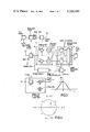
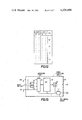
- FIG. 1 shows a block diagram of a known data transmission system with phase modulation
- FIG. 2 shows a block diagram of a known modulation stage
- FIG. 3 shows the pulse shape of a data symbol
- FIG. 4 shows a phase diagram
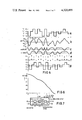
- FIG. 5a-5g show time diagrams
- FIG. 6 shows the power spectrum of a modulated signal
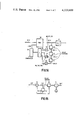
- FIG. 7 shows a block diagram of a modulation stage in accordance with the invention
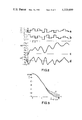
- FIG. 8a-8d show time diagrams
- FIG. 9 shows the power spectrum of a modulated signal.
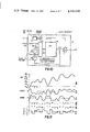
- FIG. 10 shows a block diagram of a firt level converter for use in a system according to the invention.
- FIGS. 11a-11f show time diagrams
- FIG. 12 shows a memory table for the level converter of FIG. 10,
- FIG. 13 shows a block diagram of a differential phase receiver
- FIG. 14 shows a block diagram of a universal level converter for use in a system according to the invention
- FIG. 15 shows a block diagram of a third level converter for use in a system according to the invention
- FIGS. 16a-16c show time diagrams.
- FIG. 1 shows a general block diagram of a system for transmission of multi-level data signals from a transmitter 1 to receiver 2.
- Transmitter 1 comprises a data signal source 3 which is synchronized by a clock signal source 4.
- the multi-level data signals derived from source 3 and having a symbol frequency 1/T are applied to a modulation stage 5 having a carrier oscillator 6 for generating an angle-modulated carrier signal having a substantially constant amplitude and a continuous phase.
- This modulated signal is applied to the transmission channel via an output circuit 7, wherein, as necessary, power amplification and translation to a desired radio frequency band are effected.
- receiver 2 this modulated signal is derived from the transmission channel via an input circuit 8, wherein as necessary, amplification and translation to the original frequency band is effected.
- the received modulated signal is applied to an orthogonal demodulation stage 9, comprising two product demodulators 10, 11 and two low-pass filters 12, 13, connected respectively thereto. These demodulators 10, 11 are fed by two reference carriers having a phase difference of ⁇ /2 rad.
- Two demodulated signals which are applied to a regeneration circuit 14 having two sampling circuits 15, 16 controlled by a reference clock signal, then appear at the output of low-pass filters 12 and 13, respectively.
- the samples of these two demodulated signals, thus obtained, are applied to a signal processing circuit 17 to obtain the original multi-level data signals, which are passed on to a data signal sink 18.
- receiver 2 comprises a carrier circuit 19 and a clock circuit 20 to recover the required carrier and clock signal references from the transmitted modulated signal itself.
- carrier circuit 19 which is connected directly to input circuit 8 is predominantly determined by the detection method used in the demodulation stage 9.
- differential detection the two reference carriers for each symbol interval are derived from the transmitted modulated signal in the preceding symbol interval; carrier circuit 19 can then be constructed in the manner described in Reference D(1), paragraph 10.3 and Reference D(2), paragraph 9.2.3.
- coherent detection the two reference carriers are derived from a local carrier generator whose phase is lcked onto the (non-modulated) carrier associated with the transmitted modulated signal.
- Reference D(8) comprises a construction of clock circuit 20 suitable for the present use.
- modulation stage 5 in transmitter 1 can be constructed in accordance with the functional block diagram of FIG. 2.
- This modulation stage 5 comprises a linear phase modulator 21, which is fed by carrier oscillator 6 having a constant frequency equal to the desired carrier frequency f c , the data signals of source 3 being applied to this phase modulator 21 via a filter 22 having a prescribed impulse response h(t) of a limited duration.
- phase modulator 21 has a gain factor of ⁇ /4 rad. per unit of amplitude.
- a PSK signal appears having a constant amplitude which can be expressed as:
- Time diagram a shows the 4-level data signal of source 3 to be transmitted, wherein the quaternary values "0", “1", “2” and “3” as well as the voltage values -3, -1, +1 and +3, corresponding therewith are shown.
- a PSK signal defined by formula 2
- the phase ⁇ (t) of which is shown in time diagram b for the case ⁇ (0) - ⁇ /4 rad.
- this PSK signal is multiplied by the two reference carriers, namely by sin (w c t) in demodulator 10 and by cos (w c t) in demodulator 11.
- the low-pass filters, 12, 13 can be optimized in a conventional manner (cf. reference D(5), page 981).
- the sequence of signal samples shown in time diagrams e and f appear at the output of sampling circuits 15, 16 respectively.
- Signal processing circuit 17 is arranged so that the polarity of its output value is equal to that of the signal sample at the output of circuit 16 and that the magnitude of its output value is equal to 1 for a positive polarity of the signal sample at the output of circuit 15 and equal to 3 for a negative polarity of the last-mentioned signal sample.
- the result is a regenerated 4-level data signal, which is shown in time diagram g and which--neglecting a constant delay for T/2--corresponds to the 4-level data signal to be transmitted in time diagram a.
- the described PSK system has many properties which are desirable for satisfying the above-mentioned requirements for efficient data transmission over radio links.
- the spectrum of this PSK signal at the output of modulation stage 5 is still rather wide, as appears from FIG. 6, wherein the normalised spectral power density p/T as a function of the normalised frequency
- FIG. 6 the normalised spectral power density p/T as a function of the normalised frequency
- the prior art PSK system described above furnishes an angle-modulated carrier having a constant envelope, the phase of which can assume in the centre of the symbol intervals one of the four possible values -3 ⁇ /4, - ⁇ /4, + ⁇ /4, +3 ⁇ /4.
- Such a carrier can be amplified in non-linear transmitter output stages (class-C) without the spectrum being increased.
- phase variation is added to the four possible phase changes - ⁇ /2, 0, + ⁇ /2, + ⁇ .
- a phase variation can be obtained that the spectrum is made narrower. This is based on the recognition that less power is generated outside the main lobe of the spectrum using a slight curvature of the phase variation (second tone derivative of the phase).
- the value of ⁇ (m) is determined by the preceding values ⁇ (m-1) and ⁇ (m-2)--and therefore the values k(m-1) and k(m-2)--in accordance with the rules of the following Table 2.
- the modulation stage 5 for generating an angle-modulated carrier signal having a phase ⁇ (t) in accordance with the above rules can be effected in several ways.
- modulation stage 5 is constructed as a frequency modulation stage having an ideal voltage-controlled oscillator (VCO) 6, the rest frequency f o of which is always equal to the desired carrier frequency f o and the gain constant K o of which is equal to ⁇ /2 rad. per amplitude unit per symbol interval T.
- VCO voltage-controlled oscillator
- a premodulation circuit 23 comprising the cascade arrangement of a level converter 24 for converting the 4-level data signal into a 5-level data signal and a low-pass filter 25 having a response which satisfies the third Nyquist criterion.
- This level converter 24 is arranged so that the incoming 4-level data symbols a(m) are converted into intermediate data symbols k(m) having 5 levels, the relationship of which to the 4 levels of a(m) is given in the Tables 1 and 2.
- modulation stage 5 shown in FIG. 7 will now be explained for the case in which the data symbols k(m) at the output of converter 24 appear in the form of rectangular voltage pulses having a pulse width T and a polarity and a pulse height which correspond to the values k(m).
- low-pass filter 25 has the narrowest possible bandwidth (cf. Reference D(1), pages 65), so that in view of the rectangular pulse shape chosen here filter 25 has during a period of time T of the data symbols a transfer function H(w) which is given by: ##EQU2##
- Time diagram a of FIG. 8 shows the same 4-level data signal of source 3 in FIG. 1 to be transmitted as the time diagram a of FIG. 5.
- an, intermediate 5-level data signal which is shown in time diagram b, occurs at the output of level converter 24.
- Applying this 5-level data signal b to the voltage-controlled oscillator 6 in FIG. 7 via filter 25 results in an angle-modulated carrier signal of a constant amplitude which can be expressed in the form:
- time diagram d in FIG. 8 shows the phase ⁇ (t) of the modulated signal at the output of modulation stage 5 in FIG. 2 on application of data signal a, or in other words, the phase ⁇ (t) when using the PSK method already described (see time diagram b in FIG. 5).
- the phase ⁇ (t) at the output of the voltage-controlled oscillator 6 is proportional to the integral of its input voltage u(t), so that it applies that ##EQU3## wherein, as mentioned above,
- filter 25 satisfies the third Nyquist criterion, so that it holds that ##EQU4## wherein v(t) is the output voltage of level converter 24 which, for the time interval [(mT, (m+1)T] is equal to the constant value k(m). On the basis of these formulae it holds for the phase change ⁇ (m) that
- phase ⁇ (t) for instants t within the relevant time interval [mT, (m+1)T] depends on the specific choice of filter 25, which satisfies the third Nyquist criterion. Even for the choice made here for the narrowest possible bandwidth for filter 25, the pulse response h(t) appears to have its most significant values in a central interval of the length eT, so that the form of the phase ⁇ (t) within the time intervals [mT, (m+1)T] is predominantly determined by the filtered version of the data symbols k(m) and, to a lesser extent, by the filtered version of the data symbols k(m-1) and k(m+1).
- the present modulated carrier signal has a frequency spectrum which has a narrower main lobe as well as considerably less power for frequencies outside this main lobe, than the frequency spectrum of the known PSK signal (cf. FIG. 6).
- FIG. 9 wherein for the present case the normalised spectral power density P/T as a function of the normalised frequency
- FIG. 9 shows that for frequencies f which are about twice the symbol frequency 1/T removed from the carrier frequency f c the level of the spectral power density relative to that for the carrier frequency f c is approximately 60 dB lower.
- this level is only approximately 30 dB lower for the same frequencies when the known PSK modulation stage of FIG. 2 is used, than the level for the carrier frequency f c , as shown by FIG. 6.
- the use of these measures therefore implies that for radio communication systems having the above-mentioned channel spacing of 25 kHz and 4 -level data signals having a symbol frequency of 8 kHz, the interferences in the two adjacent transmission channels have a level which is sufficiently low for the major part of the practical applications in the radio frequency range.
- modulation stage 5 which, as shown in FIG. 7 comprises a level converter 24 and a low-pass filter 25.
- level converter 24 can be constructed in many different manners, an implementation in digital techniques has many practical advantages.
- FIG. 10 shows by way of example a digital level converter 24 of a simple construction.
- the 4-level data symbols a(m) of source 3 in FIG. 1 are applied to level converter 24 in the form of 2-bit words which represent the 4 possible level "0", “1", “2", “3” of a(m).
- the value k(m) depends on the data symbol a(m) as well as on the two preceding values k(m-1) and k(m-2).
- this address A(m) is an 8-bit word which is assembled by means of an address circuit 30 from the words a(m), k(m-1) and k(m-2) in the manner shown in FIG.
- the first two bits represent data symbol a(m), the next three bits the values k(m-1) and the last three bits the value k(m-2).
- the control signals having frequency 1/T for addressing circuit 30, store 26 and digital-to-analog converter 27 originate from a time control circuit 31, which is synchronized with clock signal source 4 in FIG. 1. From the above Tables 1 and 2 it can be derived in a simple manner which 3-bit words must be stored in the storage locations.
- the rules in Table 2 then indicate which of these values, +2 or -2, must be chosen.
- the transfer function of this transversal filter forms a good and a very good approximation, respectively, of H'(w) in accordance with formula (10).
- a simple low-pass filter is connected to the output of the digital transversalfilter in order to suppress unwanted signals at the output sampling frequency and multiples thereof.
- low-pass filter 25 in FIG. 7 has the narrowest possible bandwidth, but this filter may also have a larger bandwidth.
- a transfer function having an impulse response which satisfies the third Nyquist criterion can be converted into a transfer function N 1 (w) having an impulse response which satisfies the first Nyquist criterion.
- the transfer function H(w) of filter 25 can be described in a more general form as: ##EQU6##
- Rhos Rhakukan's characteristics
- N 1 (w) N 1 (w)
- a Racos characteristic consists of a portion having a constant amplitude and a portion having a sinusoidal decreasing amplitude and can be defined by a parameter ⁇ which indicates for how much the width of the frequency band exceeds the minimum Nyquist width ⁇ /T.
- N 1 (w) for a Racos-characteristic can be written as: ##EQU7##
- the influence of the width of the frequency band of H(w), defined by formula (11) on the spectrum at the output of modulation stage 5 in FIG. 7 can then be checked by varying the parameter ⁇ of N 1 (w) in accordance with formula (12).
- ⁇ furnish an improved reduction of the power outside the band of the spectral main lobe.
- premodulation circuit 23 can now be fully realised in digital techniques by combining the above-mentioned digital construction of low-pass filter 25 with that of level converter 24 of FIG. 10, it then being possible to omit the digital-to-analog converter 27 at the output of level converter 24 in FIG. 10 and the analog-to-digital converter at the input of the digital transversal filter, because the 3-bit words k(m) read from store 26 in FIG. 10 can be directly processed in such a digital filter.
- the modulated carrier signal at the output of modulation stage 5 in FIG. 7 can be processed in the receiver 2 of FIG. 1.
- time diagram f shows the regenerated 4-level data signal at the output of signal processing circuit 17 which, not considering a constant delay for a symbol interval, corresponds to the 4-level data signal to be transmitted, as shown in time diagram a of FIG. 8.
- both values ⁇ (m) correspond to the same level "0" of the data symbol a(m).
- the Table in FIG. 12 shows these combinations and the corresponding levels of a(m).
- FIG. 13 shows a signal processing circuit 17 having a simple construction which is based on the above-mentioned considerations.
- This simple construction has been obtained by using a digital store 32 in the form of a ROM, wherein two-bit words, representing possible levels "0", “1", “2” and "3" of data signal a(m) are stored in the storage locations, these 2-bit words being read at the symbol rate 1/T and being converted into the corresponding voltage values of the data symbols a(m) by means of a digital-to-analog converter 33.
- the control signals, having frequency 1/T, for addressing circuit 34, store 32 and digital-to-analog converter 33 are obtained from a time control circuit 37 which is connected to clock circuit 20 in FIG. 1.
- the error probability as a function of the signal-to-noise ratio appears to be substantially equal in the present case to the error probability for the case when the known PSK modulation stage 5 of FIG. 2 is used.
- the use of the level converter shown in FIG. 10 results in a data transmission system which has the same desired communication properties as the known PSK systems, but which can use the available frequency spectrum in a more efficient manner than these known PSK systems owing to the remarkable reduction of the power outside the frequency band of the spectral main lobe which, in addition, is narrower than in the described example.
- a smooth variation of the phase versus the time, the second time derivative of the phase being as small as possible, is advantageous to obtain a narrow spectrum of the phase modulated signal.
- a third view may be that the phase must be kept constant as long as possible or, in other words, that the deviations of the phase or the value of the slopes in the phase variation must be kept as small as possible.
- the rule following therefrom, taking the three preceding symbol intervals into considerations, is shown in the following Table 4.
- the four-level data signal a(m) is converted into a seven-level signal k(m) and a certain phase shift is associated with each of the seven values of k(m).
- the phase shifts associated with the data symbol "2" are equal modulo -2 ⁇ .
- the symbols "0" and "3" so that a conventional prior art differential phase receiver can derive the symbols a(m) in an unambiguous manner from the phase variations ⁇ (m).
- Affecting the phase variation can be done in accordance with the above-mentioned three views, which result in the rules laid down in the following Tables 6-8.
- Table 9 shows a seven-level code wherein two opposite phase shifts of equal values are associated with each data symbol.
- phase variation from the beginning of the symbol interval can be determined.
- this phase variation amounts to + ⁇ /4 or -3 ⁇ /4 and - ⁇ /4 or +3 ⁇ /4, respectively, which phase variations are different on a modulo-2 ⁇ basis.
- a universal level converter for converting a four-level signal into a seven-level signal in accordance with the rules of Table 6, 7 or 8 is illustrated in FIG. 14. In accordance with which rules the conversion will take place will depend on the values of the coefficients a, b and c.
- the level converter comprises a ROM store 38. Applied to this store are the data symbols a(m) in the form of 2-bit words and the 2-bit words c(m), which are obtained from a comparator 39. These two 2-bit words together constitute a 4-bit address for the ROM-store. The associated value k(m) is stored at this address, for example in the form of a 3-bit word.
- the values c(m) indicate whether the expressions for f, -g or h exceed zero, are smaller than zero, or are equal to zero.
- This information is derived as follows.
- the words k(m) read from the ROM store are delayed in the delay sections 40, 41 and 42 for a time delay of one symbol interval.
- the words stored in the sections are multiplied by the above-mentioned coefficients a, b and c in the multipliers 43, 44 and 45 and thereafter added together in adder 46.
- Comparator 39 detects whether the sum exceeds zero, is smaller than zero or is equal to zero.
- the content of the ROM store 38 is specified in Table 10. It is the same for the three Tables 6, 7 and 8 when expression g in Table 7 is replaced by -g.
- the words k(m) read from the store are applied to D/A converter 47, which produces the analog seven-level signal at its output.
- D/A converter 47 which produces the analog seven-level signal at its output.
- a code in accordance with the following Table 11 with a special sequence of the symbols a(m), but in all further respects the same as the code of Table 5, can be generated by the coding circuit shown in FIG. 15.
- the four-level symbols a(m) are applied to a modulo-4 adder 48 wherein the value of the symbol b(m-1) which appears at the output of the delay section 49 is modulo-4 substracted from the value of the symbol a(m).
- the symbol b(m) appearing at the output of adder 48 is applied to delay section 49 and to the linear adder 50, wherein the symbol b(m-1) is added to the symbol b(m).
- the output signal of adder 50 is a seven-level signal having the signal levels from 0 to 6.
- the linear adder 51 adds a signal having the level -3 to the output signal of adder 50.
- the result is a seven-level signal k(m) having the levels from -3 to +3, to which the symbols a(m) are added--in accordance with Table 11--in an unambiguous manner.
- the values of the symbols a(m) can be derived from the values of k(m) by adding the value +3 modulo -4 to these values.
- phase variations ⁇ (m) associated with the symbols k(m) are determined such, that for two levels which do not differ on a modulo-4 basis (such as -1 and +3) the phase variations (- ⁇ /2, +3 ⁇ /2) do not differ on a modulo-2 basis.
- a customary phase receiver does not make any distinction between two phases which differ for 2 ⁇ , so that in this receiver no additional modulo -4 operation is necessary to derive the symbols a(m) from the phase variations ⁇ (m).
- the symbols k(m) are applied to a VCO (voltage-controlled oscillator) (FIG. 7) in such a manner that a surface unit of the multi-level signal (amplitude step 1 and a length of a symbol interval T) results in a phase variation of the oscillator signal of ⁇ /2.
- VCO voltage-controlled oscillator
- the advantageous operation of the coding circuit shown in FIG. 15 can be explained as follows.
- the probability of the occurrence of a phase variation of 0, ⁇ /2, ⁇ , 3 ⁇ /2 radians into the positive or the negative direction for a random sequence of input symbols a(m) amounts, for the device shown in FIG. 15, to, in this order, 1/4, 3/8, 1/4 and 1/8.
- the phase variations having the highest value occur with the least probability. This is an important factor for reducing the spectrum of the angle-modulated signal.
- a further factor is that the transfer characteristic of the network, formed by adder 50 and delay section 49 has a maximum at direct current. This means that the network has the tendency to counter changes in the output signal. For the phase variation this means the tendency to maintain the average slope.
- FIG. 16 wherein a pseudo-random sequence of symbols a(m) is shown in line a, the sequence of output symbols k(m) of the coding device of FIG. 15 in line b and wherein time diagram c illustrates the phase variation, assuming that the phase changes linearly in a symbol interval. From time diagram c it is seen that the phase undulates with few waves of a great amplitude and, in general, a uniform phase variation, the variations in the peaks and valleys excepted.
- phase variations are 0, 2 ⁇ /3 and 4 ⁇ /3 radians and a choice between a positive phase variation and a negative phase variation can be created for two of the levels.
Applications Claiming Priority (2)
| Application Number | Priority Date | Filing Date | Title |
|---|---|---|---|
| NL7901865 | 1979-03-08 | ||
| NL7901865A NL7901865A (nl) | 1979-03-08 | 1979-03-08 | Systeem voor multiniveau datatransmissie met behulp van een hoekgemoduleerde draaggolf van constante amplitude. |
Publications (1)
| Publication Number | Publication Date |
|---|---|
| US4320499A true US4320499A (en) | 1982-03-16 |
Family
ID=19832772
Family Applications (1)
| Application Number | Title | Priority Date | Filing Date |
|---|---|---|---|
| US06/129,796 Expired - Lifetime US4320499A (en) | 1979-03-08 | 1980-03-12 | System for multi-level data transmission by means of an angle-modulated carrier having a constant amplitude |
Country Status (14)
| Country | Link |
|---|---|
| US (1) | US4320499A (nl) |
| JP (1) | JPS55123263A (nl) |
| AU (1) | AU530112B2 (nl) |
| BE (1) | BE882111A (nl) |
| BR (1) | BR8001323A (nl) |
| CA (1) | CA1159112A (nl) |
| CH (1) | CH650117A5 (nl) |
| DE (1) | DE3008567C2 (nl) |
| DK (1) | DK152240C (nl) |
| FR (1) | FR2451136B1 (nl) |
| GB (1) | GB2044048B (nl) |
| IT (1) | IT1130303B (nl) |
| NL (1) | NL7901865A (nl) |
| SE (1) | SE450679B (nl) |
Cited By (12)
| Publication number | Priority date | Publication date | Assignee | Title |
|---|---|---|---|---|
| US4509017A (en) * | 1981-09-28 | 1985-04-02 | E-Systems, Inc. | Method and apparatus for pulse angle modulation |
| US4528526A (en) * | 1983-05-31 | 1985-07-09 | Motorola, Inc. | PSK modulator with noncollapsable output for use with a PLL power amplifier |
| US4583238A (en) * | 1982-05-10 | 1986-04-15 | Societe Anonyme Dite: Sintra-Alcatel | Synchronous data transmission system using a carrier modulated by an envelope of constant amplitude |
| US4672632A (en) * | 1984-02-03 | 1987-06-09 | Motorola, Inc. | Optimized communications system and method employing channel synthesis and phase lock detection |
| US4706261A (en) * | 1982-08-13 | 1987-11-10 | Hazeltine Corporation | Differential phase modulation |
| US4737968A (en) * | 1985-10-25 | 1988-04-12 | Phillips Petroleum Company | QPSK transmission system having phaselocked tracking filter for spectrum shaping |
| US4742533A (en) * | 1987-01-02 | 1988-05-03 | Motorola, Inc. | Soft decision digital communication apparatus |
| US4752953A (en) * | 1983-05-27 | 1988-06-21 | M/A-Com Government Systems, Inc. | Digital audio scrambling system with pulse amplitude modulation |
| US4809298A (en) * | 1985-08-30 | 1989-02-28 | Fujitsu Limited | Radio data transmission system |
| US4856025A (en) * | 1985-12-26 | 1989-08-08 | Matsushita Electric Industrial Co., Ltd. | Method of digital signal transmission |
| US20140369444A1 (en) * | 2013-06-17 | 2014-12-18 | Samsung Electronics Co., Ltd. | Transmitter, receiver, and wireless communication method thereof |
| US20150016570A1 (en) * | 2011-02-18 | 2015-01-15 | Panasonic Intellectual Property Corporation Of America | Method of signal generation and signal generating device |
Families Citing this family (2)
| Publication number | Priority date | Publication date | Assignee | Title |
|---|---|---|---|---|
| NL8402318A (nl) * | 1984-07-23 | 1986-02-17 | Philips Nv | Inrichting voor het genereren van een hoekgemoduleerd draaggolfsignaal van constante amplitude in responsie op datasignalen. |
| JPS61113346A (ja) * | 1984-11-08 | 1986-05-31 | Kyosan Electric Mfg Co Ltd | 位相偏移変調方式 |
Citations (2)
| Publication number | Priority date | Publication date | Assignee | Title |
|---|---|---|---|---|
| US3818135A (en) * | 1971-09-24 | 1974-06-18 | A Tannhauser | Circuitry for transmission of phase difference modulated data signals |
| US4109101A (en) * | 1975-06-04 | 1978-08-22 | Nippon Electric Company, Ltd. | Correlative converter between a 2n -ary code sequence and a 2n+1 -phase carrier pulse sequence |
Family Cites Families (2)
| Publication number | Priority date | Publication date | Assignee | Title |
|---|---|---|---|---|
| US3128342A (en) * | 1961-06-28 | 1964-04-07 | Bell Telephone Labor Inc | Phase-modulation transmitter |
| NL157472B (nl) * | 1968-10-02 | 1978-07-17 | Philips Nv | Ontvanger voor de ontvangst van in een voorgeschreven overdrachtsband gelegen informatiepulssignalen. |
-
1979
- 1979-03-08 NL NL7901865A patent/NL7901865A/nl not_active Application Discontinuation
-
1980
- 1980-02-28 CA CA000346636A patent/CA1159112A/en not_active Expired
- 1980-03-03 FR FR8004711A patent/FR2451136B1/fr not_active Expired
- 1980-03-05 SE SE8001700A patent/SE450679B/sv not_active IP Right Cessation
- 1980-03-05 DK DK095080A patent/DK152240C/da not_active IP Right Cessation
- 1980-03-05 CH CH1749/80A patent/CH650117A5/de not_active IP Right Cessation
- 1980-03-05 BR BR8001323A patent/BR8001323A/pt unknown
- 1980-03-05 IT IT20371/80A patent/IT1130303B/it active
- 1980-03-05 AU AU56167/80A patent/AU530112B2/en not_active Ceased
- 1980-03-05 GB GB8007491A patent/GB2044048B/en not_active Expired
- 1980-03-06 DE DE3008567A patent/DE3008567C2/de not_active Expired
- 1980-03-06 BE BE0/199697A patent/BE882111A/fr not_active IP Right Cessation
- 1980-03-08 JP JP2861680A patent/JPS55123263A/ja active Pending
- 1980-03-12 US US06/129,796 patent/US4320499A/en not_active Expired - Lifetime
Patent Citations (2)
| Publication number | Priority date | Publication date | Assignee | Title |
|---|---|---|---|---|
| US3818135A (en) * | 1971-09-24 | 1974-06-18 | A Tannhauser | Circuitry for transmission of phase difference modulated data signals |
| US4109101A (en) * | 1975-06-04 | 1978-08-22 | Nippon Electric Company, Ltd. | Correlative converter between a 2n -ary code sequence and a 2n+1 -phase carrier pulse sequence |
Cited By (21)
| Publication number | Priority date | Publication date | Assignee | Title |
|---|---|---|---|---|
| US4509017A (en) * | 1981-09-28 | 1985-04-02 | E-Systems, Inc. | Method and apparatus for pulse angle modulation |
| US4583238A (en) * | 1982-05-10 | 1986-04-15 | Societe Anonyme Dite: Sintra-Alcatel | Synchronous data transmission system using a carrier modulated by an envelope of constant amplitude |
| US4706261A (en) * | 1982-08-13 | 1987-11-10 | Hazeltine Corporation | Differential phase modulation |
| US4752953A (en) * | 1983-05-27 | 1988-06-21 | M/A-Com Government Systems, Inc. | Digital audio scrambling system with pulse amplitude modulation |
| US4528526A (en) * | 1983-05-31 | 1985-07-09 | Motorola, Inc. | PSK modulator with noncollapsable output for use with a PLL power amplifier |
| US4672632A (en) * | 1984-02-03 | 1987-06-09 | Motorola, Inc. | Optimized communications system and method employing channel synthesis and phase lock detection |
| US4809298A (en) * | 1985-08-30 | 1989-02-28 | Fujitsu Limited | Radio data transmission system |
| US4737968A (en) * | 1985-10-25 | 1988-04-12 | Phillips Petroleum Company | QPSK transmission system having phaselocked tracking filter for spectrum shaping |
| US4856025A (en) * | 1985-12-26 | 1989-08-08 | Matsushita Electric Industrial Co., Ltd. | Method of digital signal transmission |
| US4742533A (en) * | 1987-01-02 | 1988-05-03 | Motorola, Inc. | Soft decision digital communication apparatus |
| US10225123B2 (en) | 2011-02-18 | 2019-03-05 | Sun Patent Trust | Method of signal generation and signal generating device |
| US20150016570A1 (en) * | 2011-02-18 | 2015-01-15 | Panasonic Intellectual Property Corporation Of America | Method of signal generation and signal generating device |
| US9667333B2 (en) * | 2011-02-18 | 2017-05-30 | Sun Patent Trust | Method of signal generation and signal generating device |
| US10009207B2 (en) | 2011-02-18 | 2018-06-26 | Sun Patent Trust | Method of signal generation and signal generating device |
| US10476720B2 (en) | 2011-02-18 | 2019-11-12 | Sun Patent Trust | Method of signal generation and signal generating device |
| US11063805B2 (en) | 2011-02-18 | 2021-07-13 | Sun Patent Trust | Method of signal generation and signal generating device |
| US11240084B2 (en) | 2011-02-18 | 2022-02-01 | Sun Patent Trust | Method of signal generation and signal generating device |
| US11943032B2 (en) | 2011-02-18 | 2024-03-26 | Sun Patent Trust | Method of signal generation and signal generating device |
| US9847894B2 (en) * | 2013-06-17 | 2017-12-19 | Samsung Electronics Co., Ltd. | Transmitter, receiver, and wireless communication method thereof |
| US20140369444A1 (en) * | 2013-06-17 | 2014-12-18 | Samsung Electronics Co., Ltd. | Transmitter, receiver, and wireless communication method thereof |
| US10516558B2 (en) | 2013-06-17 | 2019-12-24 | Samsung Electronics Co., Ltd. | Transmitter, receiver, and wireless communication method thereof |
Also Published As
| Publication number | Publication date |
|---|---|
| IT1130303B (it) | 1986-06-11 |
| SE450679B (sv) | 1987-07-13 |
| IT8020371A0 (it) | 1980-03-05 |
| CH650117A5 (de) | 1985-06-28 |
| BE882111A (fr) | 1980-09-08 |
| DE3008567C2 (de) | 1985-08-22 |
| DK152240C (da) | 1988-07-04 |
| DE3008567A1 (de) | 1980-09-18 |
| BR8001323A (pt) | 1980-11-04 |
| CA1159112A (en) | 1983-12-20 |
| AU530112B2 (en) | 1983-06-30 |
| JPS55123263A (en) | 1980-09-22 |
| AU5616780A (en) | 1980-09-11 |
| SE8001700L (sv) | 1980-09-09 |
| GB2044048A (en) | 1980-10-08 |
| DK152240B (da) | 1988-02-08 |
| GB2044048B (en) | 1983-04-20 |
| FR2451136A1 (fr) | 1980-10-03 |
| DK95080A (da) | 1980-09-09 |
| NL7901865A (nl) | 1980-09-10 |
| FR2451136B1 (fr) | 1988-06-24 |
Similar Documents
| Publication | Publication Date | Title |
|---|---|---|
| US4229821A (en) | System for data transmission by means of an angle-modulated carrier of constant amplitude | |
| US4686688A (en) | Arrangement for generating an angle-modulated carrier signal of a constant amplitude in response to data signals | |
| US4320499A (en) | System for multi-level data transmission by means of an angle-modulated carrier having a constant amplitude | |
| FI80175C (fi) | Digitalt telekommunikationssystem, daer anvaends kvadraturmodulerade baervaogssignaler. | |
| US5459749A (en) | Multi-level superposed amplitude-modulated baseband signal processor | |
| US4338579A (en) | Frequency shift offset quadrature modulation and demodulation | |
| US4890302A (en) | Circuit for extracting carrier signals | |
| US4324001A (en) | Synchronizer for MSK burst communications | |
| EP0034383A1 (en) | Coherent receiver for angle-modulated data signals | |
| US4531221A (en) | Premodulation filter for generating a generalized tamed frequency modulated signal | |
| US4313205A (en) | Carrier synchronization and symbol synchronization for offset-QPSK burst communications | |
| US4672634A (en) | Arrangement for generating an angle-modulated carrier signal of constant amplitude in response to data signals | |
| US6996191B1 (en) | Efficient accurate controller for envelope feedforward power amplifiers | |
| US4603393A (en) | Demodulator for constant envelope and continuous phase signals which are angle modulated by a train of binary symbols | |
| US5825810A (en) | MSK spread-spectrum receiver which allows CDMA operations | |
| US6148040A (en) | Precoded gaussian minimum shift keying carrier tracking loop | |
| US4674105A (en) | Digital signal processor | |
| Chung et al. | Generalized tamed frequency modulation | |
| US5404379A (en) | Timing recovery method and system | |
| US5173924A (en) | Method for equalizing received burst signal | |
| US4726038A (en) | Digital communication system | |
| EP0614582A1 (en) | Digital demodulator for preamble-less burst communications | |
| JPH06311507A (ja) | 差動符号化4分位相遷移変調方法及びその装置 | |
| JP3178138B2 (ja) | フレーム同期回路及びフレーム同期方法 | |
| Steber | PSK demodulation (Part 1) |
Legal Events
| Date | Code | Title | Description |
|---|---|---|---|
| AS | Assignment |
Owner name: U.S. PHILIPS CORPORATION, 100 EAST 42ND ST., NEW Y Free format text: ASSIGNMENT OF ASSIGNORS INTEREST.;ASSIGNORS:MUILWIJK, DIRK;DEKKER, CORNELIS B.;DE JAGER, FRANK;REEL/FRAME:003912/0400;SIGNING DATES FROM 19800813 TO 19810313 |
|
| STCF | Information on status: patent grant |
Free format text: PATENTED CASE |