US20120249174A1 - Contact probe and semiconductor device socket including contact probe - Google Patents
Contact probe and semiconductor device socket including contact probe Download PDFInfo
- Publication number
- US20120249174A1 US20120249174A1 US13/231,016 US201113231016A US2012249174A1 US 20120249174 A1 US20120249174 A1 US 20120249174A1 US 201113231016 A US201113231016 A US 201113231016A US 2012249174 A1 US2012249174 A1 US 2012249174A1
- Authority
- US
- United States
- Prior art keywords
- plunger
- contact probe
- contacting member
- sub
- sharp
- Prior art date
- Legal status (The legal status is an assumption and is not a legal conclusion. Google has not performed a legal analysis and makes no representation as to the accuracy of the status listed.)
- Granted
Links
Images


Classifications
-
- G—PHYSICS
- G01—MEASURING; TESTING
- G01R—MEASURING ELECTRIC VARIABLES; MEASURING MAGNETIC VARIABLES
- G01R1/00—Details of instruments or arrangements of the types included in groups G01R5/00 - G01R13/00 and G01R31/00
- G01R1/02—General constructional details
- G01R1/06—Measuring leads; Measuring probes
- G01R1/067—Measuring probes
-
- H—ELECTRICITY
- H01—ELECTRIC ELEMENTS
- H01R—ELECTRICALLY-CONDUCTIVE CONNECTIONS; STRUCTURAL ASSOCIATIONS OF A PLURALITY OF MUTUALLY-INSULATED ELECTRICAL CONNECTING ELEMENTS; COUPLING DEVICES; CURRENT COLLECTORS
- H01R11/00—Individual connecting elements providing two or more spaced connecting locations for conductive members which are, or may be, thereby interconnected, e.g. end pieces for wires or cables supported by the wire or cable and having means for facilitating electrical connection to some other wire, terminal, or conductive member, blocks of binding posts
- H01R11/11—End pieces or tapping pieces for wires, supported by the wire and for facilitating electrical connection to some other wire, terminal or conductive member
- H01R11/18—End pieces terminating in a probe
-
- G—PHYSICS
- G01—MEASURING; TESTING
- G01R—MEASURING ELECTRIC VARIABLES; MEASURING MAGNETIC VARIABLES
- G01R1/00—Details of instruments or arrangements of the types included in groups G01R5/00 - G01R13/00 and G01R31/00
- G01R1/02—General constructional details
- G01R1/04—Housings; Supporting members; Arrangements of terminals
- G01R1/0408—Test fixtures or contact fields; Connectors or connecting adaptors; Test clips; Test sockets
- G01R1/0433—Sockets for IC's or transistors
- G01R1/0483—Sockets for unleaded IC's having matrix type contact fields, e.g. BGA or PGA devices; Sockets for unpackaged, naked chips
-
- G—PHYSICS
- G01—MEASURING; TESTING
- G01R—MEASURING ELECTRIC VARIABLES; MEASURING MAGNETIC VARIABLES
- G01R1/00—Details of instruments or arrangements of the types included in groups G01R5/00 - G01R13/00 and G01R31/00
- G01R1/02—General constructional details
- G01R1/06—Measuring leads; Measuring probes
- G01R1/067—Measuring probes
- G01R1/06711—Probe needles; Cantilever beams; "Bump" contacts; Replaceable probe pins
- G01R1/06716—Elastic
- G01R1/06722—Spring-loaded
-
- G—PHYSICS
- G01—MEASURING; TESTING
- G01R—MEASURING ELECTRIC VARIABLES; MEASURING MAGNETIC VARIABLES
- G01R1/00—Details of instruments or arrangements of the types included in groups G01R5/00 - G01R13/00 and G01R31/00
- G01R1/02—General constructional details
- G01R1/06—Measuring leads; Measuring probes
- G01R1/067—Measuring probes
- G01R1/06711—Probe needles; Cantilever beams; "Bump" contacts; Replaceable probe pins
- G01R1/06733—Geometry aspects
- G01R1/06738—Geometry aspects related to tip portion
-
- G—PHYSICS
- G01—MEASURING; TESTING
- G01R—MEASURING ELECTRIC VARIABLES; MEASURING MAGNETIC VARIABLES
- G01R31/00—Arrangements for testing electric properties; Arrangements for locating electric faults; Arrangements for electrical testing characterised by what is being tested not provided for elsewhere
- G01R31/26—Testing of individual semiconductor devices
-
- H—ELECTRICITY
- H01—ELECTRIC ELEMENTS
- H01R—ELECTRICALLY-CONDUCTIVE CONNECTIONS; STRUCTURAL ASSOCIATIONS OF A PLURALITY OF MUTUALLY-INSULATED ELECTRICAL CONNECTING ELEMENTS; COUPLING DEVICES; CURRENT COLLECTORS
- H01R13/00—Details of coupling devices of the kinds covered by groups H01R12/70 or H01R24/00 - H01R33/00
- H01R13/02—Contact members
- H01R13/22—Contacts for co-operating by abutting
- H01R13/24—Contacts for co-operating by abutting resilient; resiliently-mounted
- H01R13/2407—Contacts for co-operating by abutting resilient; resiliently-mounted characterized by the resilient means
- H01R13/2421—Contacts for co-operating by abutting resilient; resiliently-mounted characterized by the resilient means using coil springs
-
- H—ELECTRICITY
- H01—ELECTRIC ELEMENTS
- H01R—ELECTRICALLY-CONDUCTIVE CONNECTIONS; STRUCTURAL ASSOCIATIONS OF A PLURALITY OF MUTUALLY-INSULATED ELECTRICAL CONNECTING ELEMENTS; COUPLING DEVICES; CURRENT COLLECTORS
- H01R13/00—Details of coupling devices of the kinds covered by groups H01R12/70 or H01R24/00 - H01R33/00
- H01R13/02—Contact members
- H01R13/22—Contacts for co-operating by abutting
- H01R13/24—Contacts for co-operating by abutting resilient; resiliently-mounted
- H01R13/2464—Contacts for co-operating by abutting resilient; resiliently-mounted characterized by the contact point
- H01R13/2485—Contacts for co-operating by abutting resilient; resiliently-mounted characterized by the contact point for contacting a ball
-
- H—ELECTRICITY
- H01—ELECTRIC ELEMENTS
- H01R—ELECTRICALLY-CONDUCTIVE CONNECTIONS; STRUCTURAL ASSOCIATIONS OF A PLURALITY OF MUTUALLY-INSULATED ELECTRICAL CONNECTING ELEMENTS; COUPLING DEVICES; CURRENT COLLECTORS
- H01R33/00—Coupling devices specially adapted for supporting apparatus and having one part acting as a holder providing support and electrical connection via a counterpart which is structurally associated with the apparatus, e.g. lamp holders; Separate parts thereof
- H01R33/74—Devices having four or more poles, e.g. holders for compact fluorescent lamps
- H01R33/76—Holders with sockets, clips, or analogous contacts adapted for axially-sliding engagement with parallely-arranged pins, blades, or analogous contacts on counterpart, e.g. electronic tube socket
-
- H—ELECTRICITY
- H10—SEMICONDUCTOR DEVICES; ELECTRIC SOLID-STATE DEVICES NOT OTHERWISE PROVIDED FOR
- H10P—GENERIC PROCESSES OR APPARATUS FOR THE MANUFACTURE OR TREATMENT OF DEVICES COVERED BY CLASS H10
- H10P74/00—Testing or measuring during manufacture or treatment of wafers, substrates or devices
Definitions
- the present disclosure relates to a contact probe and a semiconductor device socket including the contact probe.
- a semiconductor device socket is provided with a contact probe as a connector for electrically connecting a semiconductor device such as an integrated circuit (IC) package having solder balls or solder bumps as electrodes to a testing circuit board of a testing instrument.
- the contact probe provided in such a semiconductor device socket includes: a plunger for contacting a solder ball of an IC package; and a coil spring for exerting, on the plunger, elastic urging force for bringing the contact probe in contact with the solder ball at given pressure (refer to Japanese Patent Application Publication No. JP-A-2004-152495 and Japanese Patent Application Publication No. JP-A-2003-167001, for example).
- the contact probe is provided with a contacting member having plural sharp contact portions.
- the contacting member is provided at the tip of a plate-like plunger (refer to JP-A-2004-152495) or a cylindrical plunger (refer to JP-A-2003-167001) having a given shape which is produced by punching (pressing) sheet metal.
- the contacting member of the plunger is brought into point contact with and sticks into an electrode by elastic urging force of the coil spring, whereby the oxide coating of the electrode is broken and good contact is obtained.
- An electrode of a semiconductor device is in various forms such as a bump formed of a substantially spherical solder ball or a flat-plate-like pad.
- the substantially spherical solder ball as a bump is not necessarily a complete sphere and varies in position and size.
- the plural contact portions of a contacting member of a plunger contact the solder ball uniformly; the manner of contact tends to vary to render the contact unstable.
- the surface of the solder is not only covered with an oxide coating but also foreign substances may be stuck to the surface.
- solder or foreign substances may be transferred from the electrode to the contacting member of the plunger. In this case, it is difficult to remove such a solder or foreign substances stuck to the contacting member.
- oxide coatings may also be formed on the surfaces of solder fragments transferred to the contacting member of the plunger. Such oxide coatings may increase the contact resistance, making it impossible to maintain a good electrical connection.
- Illustrative aspects of the present invention provide a contact probe which makes it possible to test a semiconductor device smoothly and properly by bringing a contacting member into stable contact with an electrode of the semiconductor device by suppressing the increase of the contact resistance between the electrode and the contacting member, as well as also providing to a semiconductor device socket including the contact probe.
- a contact probe includes: a plunger; a top contacting member which is provided at a tip end of the plunger and is brought into contact with an electrode of a semiconductor device; a bottom contacting member which is brought into contact with an electrode of a testing board; and an elastic member for urging the top contacting member and the bottom contacting member in opposite directions away from each other, wherein the plunger is formed into a cylindrical shape and includes a through-hole which penetrates through the plunger in an axial direction thereof, wherein the top contacting member includes a plurality of mountain-shaped sharp portions which are formed at the tip end of the plunger, and wherein each of the sharp portions is asymmetrical with respect to a straight line that passes through a peak of the sharp portion and extends along an axial direction of the plunger, and is bent toward a center line of the plunger.
- FIG. 1 is a perspective view showing a contact probe according to a first exemplary embodiment of the present invention.
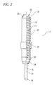
- FIG. 2 is a side view in which a half part of the contact probe of FIG. 1 is shown in cross-section.
- FIG. 3 is an exploded view showing the contact probe shown in FIG. 1 .
- FIGS. 4A and 4B are a plan view and a side view, respectively, of a plunger which constitutes the contact probe shown in FIG. 1 .
- FIG. 5 is a perspective view, as viewed obliquely from above, of the plunger which constitutes the contact probe shown in FIG. 1 .
- FIGS. 6A to 6C are cross-sectional views showing example shapes of each sharp portion of a top contacting member of the plunger.
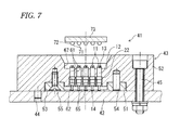
- FIG. 7 is a cross-sectional view showing an example configuration of a semiconductor device socket according to the first exemplary embodiment.
- FIG. 8 is a cross-sectional view showing an operation of the semiconductor device socket shown in FIG. 7 .
- FIGS. 9A to 9C are side views showing how a solder ball comes into contact with a top contacting member.
- FIG. 10 is a cross-sectional view showing the top contacting member of the plunger and showing how each sharp portion of the top contacting member is bent.
- FIGS. 11A to 11E are perspective views showing a manufacturing process of the plunger by cutting.
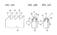
- FIGS. 12A to 12C are views showing a manufacturing process of the plunger by press working in which FIG. 12A is a plan view of a metal sheet and FIGS. 12B and 12C are perspective views of the plunger.
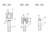
- FIGS. 13A to 13C are side views showing how the top contacting member of the plunger is formed.
- FIGS. 14A to 14C are cross-sectional views showing how a coil spring and a sub-plunger are attached to the plunger.
- FIGS. 15A and 15B are views showing a manufacturing process of a plunger of a contact probe according to another exemplary embodiment of the present invention in which FIG. 15A is a plan view of a metal sheet and FIG. 15B is a perspective view of a manufactured plunger.
- FIG. 16 is a side view in which a half part of the contact probe further according to another exemplary embodiment is shown in cross-section.
- FIGS. 17A to 17E are perspective views showing plungers of contact probes according to further exemplary embodiments of the present invention, respectively.
- the contact probe 11 is provided with a plunger 12 which is made of a conductive metal material.
- the plunger 12 has a top contacting member 13 at its tip, which is the top of the plunger 12 .
- the contact probe 11 has a bottom contacting member 14 at the bottom thereof.
- the plunger 12 is a cylinder having a through-hole 15 , which extends in an axial direction thereof.
- a sub-plunger 16 is provided under the plunger 12 .
- the sub-plunger 16 is made of a conductive metal material and the bottom end portion of the sub-plunger 16 is formed as the bottom contacting member 14 .
- a coil spring (elastic member) 17 whose outer diameter is slightly smaller than a diameter of the through-hole 15 of the plunger 12 is housed in the through-hole 15 .
- the coil spring 17 is made of spring steel, and produces an elastic force that urges the sub-plunger 16 downward against the bottom end portion the plunger 12 .
- the top contacting member 13 of the plunger 12 and the bottom contacting member 14 of the sub-plunger 16 are urged by the coil spring 17 in opposite directions away from each other.
- the top contacting member 13 which is provided at the tip of the plunger 12 , includes a plurality of (in this exemplary embodiment, four) mountain-shaped sharp portions 25 .
- Each sharp portion 25 has ridges 27 a and 27 b formed on both sides of a peak 26 .
- each sharp portion 25 is asymmetrical with respect to a straight line A, which is parallel with the axial line of the plunger 12 , passing through the peak 26 .
- the ridges 27 a and 27 b of each sharp portion 25 have different lengths. More specifically, the ridge 27 b is shorter than the ridge 27 a.
- the cylindrical plunger 12 is formed with a flange 22 , which extends in a circumferential direction of the plunger 12 and projects outward.
- each sharp portion 25 of the top contacting member 13 is bent toward a center line of the plunger 12 .
- a diameter of a circle passing through the peaks 26 of the respective sharp potions 25 is smaller than that of the through-hole 15 of the plunger 12 , and is also smaller than an outer diameter of the coil spring 17 . Therefore, the top end of the coil spring 17 is in contact with inner surfaces of the sharp portions 25 (see FIG. 2 ) and is thereby prevented from losing contact with the top end of the plunger 12 .
- each sharp portion 25 may become thinner gradually toward the peak 26 .
- each sharp portion 25 may be gradually curved inward.
- a narrow portion 29 whose diameter decreases gradually downward may be formed at the bottom of the plunger 12 .
- the sub-plunger 16 has a cylindrical rod portion 31 and a flange 32 , which is formed at a middle position, in the axial direction, of the rod portion 31 .
- the bottom end portion of the rod portion 31 is the bottom contacting member 14 .
- An outer diameter of the rod portion 31 is slightly smaller than an inner diameter of the coil spring 17
- an outer diameter of the flange 32 is larger than the inner diameter of the coil spring 17 and is slightly smaller than the diameter of the through-hole 15 of the plunger 12 .
- An upper portion of the rod portion 31 of the sub-plunger 16 is inserted in the coil spring 17 , and the flange 32 is in contact with the coil spring 17 .
- the sub-plunger 16 is housed in the through-hole 15 of the plunger 12 , and is urged by the urging force of the coil spring 17 and thereby engages with the narrow portion 29 of the plunger 12 so as not to lose contact with the plunger 12 at its bottom end.
- the coil spring 17 is housed in the through-hole 15 of the plunger 12 in a compressed state.
- the plunger 12 and the sub-plunger 16 are urged by the coil spring 17 in opposite directions away from each other.
- the top contacting member 13 and the bottom contacting member 14 are thus urged by the coil spring 17 in opposite directions away from each other.
- the semiconductor device socket 41 has a probe housing block 43 , is positioned with respect to a testing board 42 by a positioning pin 44 , and is fixed to the testing board 42 with a fastening bolt 45 .
- the probe housing block 43 includes a contacting member arrangement board 51 and a socket board 52 both of which are insulators.
- the socket board 52 is formed with an arrangement board housing recess 53 on the bottom surface side.
- the contacting member arrangement board 51 is fitted in the arrangement board housing recess 53 , positioned with respect to the socket board 52 by a positioning pin 54 , and fixed (screwed) to the socket board 52 with a screw 55 .
- the socket board 52 is formed with plural probe housing holes 61 which house respective contact probes 11 , which are inserted from below the probe housing holes 61 .
- Each probe housing hole 61 is formed with a step 62 at a middle position in an axial direction thereof.
- the portion, above the step 62 , of each probe housing hole 61 is smaller in diameter than the flange 22 and the position, below the step 62 , of each probe housing hole 61 is slightly larger in diameter than the flange 22 .
- the contacting member arrangement board 51 which is fixed to the socket board 52 , is formed with plural contacting member holding holes 65 so as to correspond to the respective probe housing holes 61 .
- the bottom contacting members 14 of the contact probes 11 housed in the probe housing holes 61 are inserted in the contacting member holding holes 65 , respectively.
- the bottom contacting members 14 of the contact probes 11 are held by the respective contacting member holding holes 65 and thereby set at given positions of the testing board 42 .
- the testing board 42 is provided with electrodes (not shown) at the positions where the bottom contacting members 14 of the contact probes 11 are located, whereby each of the electrodes is in electrical contact with a respective one of the bottom contacting members 14 of the contact probes 11 .
- the socket board 52 is formed with a socket recess 67 on the top surface side thereof.
- a semiconductor device 73 which has a bottom surface formed with plural electrodes 72 having solder balls 71 , can be inserted into the socket recess 67 from above.
- the semiconductor device 73 When testing the semiconductor device 73 using the above-configured semiconductor device socket 41 , the semiconductor device 73 is inserted into the socket recess 67 of the socket board 52 . In this state, as shown in FIG. 8 , the semiconductor device 73 is pressed downward by a pressing member 75 . As a result, the semiconductor device 73 is pressed down in the socket recess 67 , and, as shown in FIG. 9A , the solder ball 71 of each electrode 72 approaches the top contacting member 13 of the corresponding contact probe 11 . Then, as shown in FIG. 9B , each solder ball 71 is pressed against and comes into contact with the corresponding top contacting member 13 .
- Each sharp portion 25 of the top contacting member 13 of each contact probe 11 is formed in a mountain-shape and, as shown in FIGS. 1 and 4B , is asymmetrical with respect to the straight line A that passes through the peak 26 and extends parallel with the axial line of the plunger 12 . Therefore, the peak portion of each sharp portion 25 slightly digs into the solder ball 71 , which is being pressed against the top contacting member 13 . As a result, the solder ball 71 is displaced in a direction that crosses the axial direction along each longer ridge 27 a. Thus, as shown in FIG. 9B , the solder ball 71 and each sharp portion 25 slide slightly with respect to each other when being pressed against each other.
- each sharp portion 25 is bent toward the center line of the plunger 12 , as shown in FIG. 10 , each sharp portion 25 is elastically deformed inward (indicated by an arrow in FIG. 10 ) due to being pressed by the solder ball 71 . If the solder ball 71 and the contact probe 11 are deviated from each other, a sharp portion 25 that receives a heavier load than the other sharp portions 25 is elastically deformed inward more than the other sharp portions 25 , whereby differences of the distances between the solder ball 71 and the sharp portions 25 are absorbed and the sharp portions 25 come to contact the solder ball 71 uniformly. In this manner, electrical continuity is established reliably between the electrodes 72 of the semiconductor device 73 and the electrodes of the testing board 42 via the contact probes 11 , which enables a test of the semiconductor device 73 .
- each sharp portion 25 of the top contacting member 13 is formed in a mountain-shape so as to be asymmetrical with respect to the straight line A that passes through the peak 26 and extends along the axial line of the plunger 12 .
- This causes a solder ball 71 to slide along the longer ridge 27 a of each sharp portion 25 and to be brought into line contact with the longer ridge 27 a.
- electrical continuity is established reliably and stably between an active solder portion of the solder ball 71 and each sharp portion 25 of the top contacting member 13 .
- Each sharp portion 25 is bent toward the center line of the plunger 12 and hence is apt to be deformed toward the center side. Therefore, even if a solder ball 71 and a contact probe 11 are deviated from each other, the sharp portions 25 are elastically deformed, whereby differences of the distances between the solder ball 71 and the sharp portions 25 are absorbed and the sharp portions 25 come to contact the solder ball 71 uniformly.
- each sharp portion 25 is shaped so as to decrease in thickness toward the peak 26 , each sharp portion 25 is more apt to be deformed elastically, which can allow the sharp portions 25 to contact a solder ball 71 with a higher level of uniformity.
- the semiconductor device socket 41 including the contact probes 11 can reliably establish electrical continuity between the electrodes 72 of the semiconductor device 73 and the electrodes of the testing board 42 via the contact probes 11 , and hence can maintain high reliability of a number of tests carried out on semiconductor devices 73 .
- the contact probe 11 can be manufactured relatively easily by forming the plunger 12 by cutting or press working and attaching the coil spring 17 and the sub-plunger 16 to the plunger 12 .
- an exemplary manufacturing method of the contact probe 11 will be outlined below.
- the plunger 12 may be formed using cutting. Specifically, as shown in FIG. 11 a , a cylindrical body 81 , which will become the plunger 12 , is formed by first using a lathe or the like to form a through-hole 15 , which the coil spring 17 can be inserted into, at one end of a metal rod made of a copper or iron-based material. The thickness of the cylindrical body 81 is set to be such a value that the resulting plunger 12 will be strong enough to endure the load that will act on the plunger 12 during testing of a semiconductor device 73 . As shown in FIG. 11B , the top contacting member 13 of the plunger 12 is then formed by cutting the tip portion of the cylindrical body 81 into a tapered shape. As shown in FIG. 11C , a V-shaped cut 82 is then formed by cutting the tapered tip portion of the cylindrical body 81 .
- V-shaped cuts 82 are then formed at plural positions while the cylindrical body 81 is rotated for form the plurality of mountain-shaped sharp portions 25 of the plunger.
- Each sharp portion 25 is formed so as to be asymmetrical with respect to the straight line A (see FIGS. 1 and 4B ) that passes through the peak 26 and that extends along the axial line of the cylindrical body 81 .
- each sharp portion 25 is bent toward the center line of the cylindrical body 81 .
- the rod is cut to form the cylindrical body 81 and the cylindrical body 81 is subjected to various kinds of surface treatment such as nickel plating or gold plating depending on the material to complete the formation of the plunger 12 .
- the plunger 12 may also be formed using press working. Specifically, as shown in FIG. 12A , first a metal sheet 85 made of a copper or iron-based material is punched using metal dies and a pressing machine or the like. The thickness of the metal sheet 85 is set to be such a value that the resulting plunger 12 will be strong enough to endure the load that will act on the plunger 12 during testing of a semiconductor device 73 . By such press working, plural V-shaped cuts 86 are formed in one side end portion of the metal sheet 85 to form the mountain-shaped sharp potions 25 . Each sharp portion 25 is shaped so as to be asymmetrical with respect to the vertical line (as viewed in FIG. 12A ) passing through its peak.
- a cylindrical body having a through-hole 15 into which the coil spring 17 can be inserted is formed by bending the metal sheet 85 .
- each sharp portion 25 is bent toward the center line of the cylindrical body for form the tip portion.
- the cylindrical body is subjected to various kinds of surface treatment such as nickel plating or gold plating depending on the material to complete the formation of the plunger 12 .
- a forming jig 91 is used to bend the sharp portions 25 toward the center line of the plunger 12 to form the top contacting member 13 of the plunger 12 .
- the forming jig 91 is formed with a forming recess 92 which has a tapered wall 93 which gradually narrows toward the inside end thereof.
- the top portion of the plunger 12 is pressed into the forming recess 92 of the forming jig 91 , whereby the tip sharp potions 25 of the plunger 12 are bent so as to conform to the tapered wall 93 of the forming recess 92 .
- the plunger 12 having the sharp portions 25 that are bent toward the center line of the plunger 12 is obtained as shown in FIG. 13C .
- An assembling jig 95 shown in FIG. 14A is used to attach the coil spring 17 and the sub-plunger 16 to the thus-manufactured plunger 12 .
- the assembling jig 95 is formed with a crimping recess 96 which has a crimping wall 97 which narrows gradually toward the bottom end thereof. Further, a holding recess 98 is formed at a bottom of the assembling jig 95 .
- the coil spring 17 and the sub-plunger 16 are inserted in order into the through-hole 15 of the plunger 12 from below. Then, as shown in FIG. 14B , the sub-plunger 16 is pressed into the crimping recess 96 of the assembling jig 95 , whereby the bottom contacting member 14 of the sub-plunger 16 comes into contact with the bottom surface of the holding recess 98 and is thereby prevented from moving downward further. As a result, the sub-plunger 16 goes into the through-hole 15 of the plunger 12 while compressing the coil spring 17 .
- the contact probe 11 can be manufactured easily by either cutting or press working. Therefore, the contact probe 11 can be manufactured efficiently by selecting an optimum working method for a production situation such as small-quantity production or mass production. Furthermore, cost increase etc. due to production of unnecessary dies can be prevented.
- each sharp portion 25 of the contact probe 11 is not limited to the shapes described in the first exemplary embodiment.
- FIGS. 15A and 15B show sharp portions 25 A having a different shape.
- ridges 27 a and 27 b are located on the same single side with respect to a straight line A that passes through a peak 26 and extends along the axial line of the plunger 12 .
- the sharp portion 25 A can be elastically deformed more easily by a load that acts on the sharp portion 25 A in testing a semiconductor device 73 . Therefore, the contact probe 11 can contact a solder ball 71 with an even higher level of uniformity.
- a plurality of V-shaped cuts 86 are formed by punching in one side end portion of a metal sheet 85 to form mountain-shaped sharp potions 25 A.
- Each sharp portion 25 A is shaped so as to be asymmetrical with respect to the straight line A passing through its peak 26 and so that the ridges 27 a and 27 b are located on the same single side of the straight line A.
- a cylindrical body having a through-hole 15 into which the coil spring 17 can be inserted is formed by bending the metal sheet 85 .
- FIG. 16 shows a contact probe 11 A in which a bottom end portion of a coil spring 17 A serves as a bottom contacting member 14 (the sub-plunger 16 is not used).
- a rod-like portion 17 a is formed such that the winding diameter is reduced and one-pitch portions are in close contact with each other in the axial direction. Further, the rod-like portion 17 a projects through the bottom opening of the plunger 12 . In the contact probe 11 A, a bottom end portion of the rod-like portion 17 a serves as the bottom contacting member 14 . The thus-configured contact probe 11 A enables cost reduction because the number of components is reduced.
- the number of sharp portions 25 constituting the top contacting member 13 of the plunger 12 is not limited to four; satisfactory results may be obtained as long as a plurality of sharp portions 25 are provided.
- FIG. 17A shows a top contacting member 13 B in which two sharp portions 25 are opposed to each other
- FIG. 17B shows a top contacting member 13 C in which three sharp portions 25 are arranged at equal intervals in a circumferential direction of the plunger 12 .
- FIG. 17C shows a top contacting member 13 D in which five sharp portions 25 are arranged at equal intervals in the circumferential direction of the plunger 12
- FIG. 17D shows a top contacting member 13 E in which six sharp portions 25 are arranged at equal intervals in the circumferential direction
- FIG. 17E shows a top contacting member 13 F in which eight sharp portions 25 are arranged at equal intervals in the circumferential direction.
Landscapes
- Physics & Mathematics (AREA)
- General Physics & Mathematics (AREA)
- Engineering & Computer Science (AREA)
- Computer Hardware Design (AREA)
- Microelectronics & Electronic Packaging (AREA)
- Geometry (AREA)
- Measuring Leads Or Probes (AREA)
- Testing Of Individual Semiconductor Devices (AREA)
Abstract
Description
- This application claims priority from Japanese Patent Application No. 2011-073345, filed on Mar. 29, 2011, the entire contents of which are hereby incorporated by reference.
- The present disclosure relates to a contact probe and a semiconductor device socket including the contact probe.
- A semiconductor device socket is provided with a contact probe as a connector for electrically connecting a semiconductor device such as an integrated circuit (IC) package having solder balls or solder bumps as electrodes to a testing circuit board of a testing instrument. The contact probe provided in such a semiconductor device socket includes: a plunger for contacting a solder ball of an IC package; and a coil spring for exerting, on the plunger, elastic urging force for bringing the contact probe in contact with the solder ball at given pressure (refer to Japanese Patent Application Publication No. JP-A-2004-152495 and Japanese Patent Application Publication No. JP-A-2003-167001, for example).
- In order to establish a good electrical connection between an electrode and a contact probe, it is necessary to remove an oxide coating formed on a surface of the electrode. Therefore, the contact probe is provided with a contacting member having plural sharp contact portions. The contacting member is provided at the tip of a plate-like plunger (refer to JP-A-2004-152495) or a cylindrical plunger (refer to JP-A-2003-167001) having a given shape which is produced by punching (pressing) sheet metal. The contacting member of the plunger is brought into point contact with and sticks into an electrode by elastic urging force of the coil spring, whereby the oxide coating of the electrode is broken and good contact is obtained.
- An electrode of a semiconductor device is in various forms such as a bump formed of a substantially spherical solder ball or a flat-plate-like pad. In particular, the substantially spherical solder ball as a bump is not necessarily a complete sphere and varies in position and size. As a result, it is rare that the plural contact portions of a contacting member of a plunger contact the solder ball uniformly; the manner of contact tends to vary to render the contact unstable. Furthermore, the surface of the solder is not only covered with an oxide coating but also foreign substances may be stuck to the surface. In order to bring a contacting member in stable contact with an active solder, it is necessary to cause the contacting member to bury into an electrode by applying strong pressure to the contacting member. However, this may damage the electrode.
- When the sharp contacting member of the plunger is caused to bury into the solder ball of the electrode by contact pressure, solder or foreign substances may be transferred from the electrode to the contacting member of the plunger. In this case, it is difficult to remove such a solder or foreign substances stuck to the contacting member. In particular, when contacting operations are performed repeatedly, oxide coatings may also be formed on the surfaces of solder fragments transferred to the contacting member of the plunger. Such oxide coatings may increase the contact resistance, making it impossible to maintain a good electrical connection.
- Illustrative aspects of the present invention provide a contact probe which makes it possible to test a semiconductor device smoothly and properly by bringing a contacting member into stable contact with an electrode of the semiconductor device by suppressing the increase of the contact resistance between the electrode and the contacting member, as well as also providing to a semiconductor device socket including the contact probe.
- According to a first aspect of the invention, a contact probe includes: a plunger; a top contacting member which is provided at a tip end of the plunger and is brought into contact with an electrode of a semiconductor device; a bottom contacting member which is brought into contact with an electrode of a testing board; and an elastic member for urging the top contacting member and the bottom contacting member in opposite directions away from each other, wherein the plunger is formed into a cylindrical shape and includes a through-hole which penetrates through the plunger in an axial direction thereof, wherein the top contacting member includes a plurality of mountain-shaped sharp portions which are formed at the tip end of the plunger, and wherein each of the sharp portions is asymmetrical with respect to a straight line that passes through a peak of the sharp portion and extends along an axial direction of the plunger, and is bent toward a center line of the plunger.
- Other aspects and advantages of the invention will be apparent from the following description, the drawings and the claims.
-
FIG. 1 is a perspective view showing a contact probe according to a first exemplary embodiment of the present invention. -
FIG. 2 is a side view in which a half part of the contact probe ofFIG. 1 is shown in cross-section. -
FIG. 3 is an exploded view showing the contact probe shown inFIG. 1 . -
FIGS. 4A and 4B are a plan view and a side view, respectively, of a plunger which constitutes the contact probe shown inFIG. 1 . -
FIG. 5 is a perspective view, as viewed obliquely from above, of the plunger which constitutes the contact probe shown inFIG. 1 . -
FIGS. 6A to 6C are cross-sectional views showing example shapes of each sharp portion of a top contacting member of the plunger. -
FIG. 7 is a cross-sectional view showing an example configuration of a semiconductor device socket according to the first exemplary embodiment. -
FIG. 8 is a cross-sectional view showing an operation of the semiconductor device socket shown inFIG. 7 . -
FIGS. 9A to 9C are side views showing how a solder ball comes into contact with a top contacting member. -
FIG. 10 is a cross-sectional view showing the top contacting member of the plunger and showing how each sharp portion of the top contacting member is bent. -
FIGS. 11A to 11E are perspective views showing a manufacturing process of the plunger by cutting. -
FIGS. 12A to 12C are views showing a manufacturing process of the plunger by press working in whichFIG. 12A is a plan view of a metal sheet andFIGS. 12B and 12C are perspective views of the plunger. -
FIGS. 13A to 13C are side views showing how the top contacting member of the plunger is formed. -
FIGS. 14A to 14C are cross-sectional views showing how a coil spring and a sub-plunger are attached to the plunger. -
FIGS. 15A and 15B are views showing a manufacturing process of a plunger of a contact probe according to another exemplary embodiment of the present invention in whichFIG. 15A is a plan view of a metal sheet andFIG. 15B is a perspective view of a manufactured plunger. -
FIG. 16 is a side view in which a half part of the contact probe further according to another exemplary embodiment is shown in cross-section. -
FIGS. 17A to 17E are perspective views showing plungers of contact probes according to further exemplary embodiments of the present invention, respectively. - A contact probe and a semiconductor device socket including the contact probe according to a first exemplary embodiment of the present invention will hereinafter be described with reference to the drawings. As shown in
FIG. 1 , thecontact probe 11 according to the first exemplary embodiment is provided with aplunger 12 which is made of a conductive metal material. Theplunger 12 has a top contactingmember 13 at its tip, which is the top of theplunger 12. Thecontact probe 11 has abottom contacting member 14 at the bottom thereof. - As shown in
FIGS. 2 and 3 , theplunger 12 is a cylinder having a through-hole 15, which extends in an axial direction thereof. Asub-plunger 16 is provided under theplunger 12. Thesub-plunger 16 is made of a conductive metal material and the bottom end portion of thesub-plunger 16 is formed as thebottom contacting member 14. - In the
contact probe 11, a coil spring (elastic member) 17 whose outer diameter is slightly smaller than a diameter of the through-hole 15 of theplunger 12 is housed in the through-hole 15. Thecoil spring 17 is made of spring steel, and produces an elastic force that urges the sub-plunger 16 downward against the bottom end portion theplunger 12. As a result, thetop contacting member 13 of theplunger 12 and thebottom contacting member 14 of the sub-plunger 16 are urged by thecoil spring 17 in opposite directions away from each other. - As shown in
FIGS. 4A , 4B andFIG. 5 , thetop contacting member 13, which is provided at the tip of theplunger 12, includes a plurality of (in this exemplary embodiment, four) mountain-shapedsharp portions 25. Eachsharp portion 25 hasridges peak 26. As shown inFIG. 4B , eachsharp portion 25 is asymmetrical with respect to a straight line A, which is parallel with the axial line of theplunger 12, passing through thepeak 26. As a result, theridges sharp portion 25 have different lengths. More specifically, theridge 27 b is shorter than theridge 27 a. As shown inFIGS. 1 to 5 , thecylindrical plunger 12 is formed with aflange 22, which extends in a circumferential direction of theplunger 12 and projects outward. - As shown in
FIG. 6A , eachsharp portion 25 of the top contactingmember 13 is bent toward a center line of theplunger 12. As a result, a diameter of a circle passing through thepeaks 26 of the respectivesharp potions 25 is smaller than that of the through-hole 15 of theplunger 12, and is also smaller than an outer diameter of thecoil spring 17. Therefore, the top end of thecoil spring 17 is in contact with inner surfaces of the sharp portions 25 (seeFIG. 2 ) and is thereby prevented from losing contact with the top end of theplunger 12. As shown inFIG. 6B , eachsharp portion 25 may become thinner gradually toward thepeak 26. As shown inFIG. 6C , eachsharp portion 25 may be gradually curved inward. As shown inFIG. 2 , anarrow portion 29 whose diameter decreases gradually downward may be formed at the bottom of theplunger 12. - As shown in
FIGS. 2 and 3 , the sub-plunger 16 has acylindrical rod portion 31 and aflange 32, which is formed at a middle position, in the axial direction, of therod portion 31. The bottom end portion of therod portion 31 is thebottom contacting member 14. An outer diameter of therod portion 31 is slightly smaller than an inner diameter of thecoil spring 17, and an outer diameter of theflange 32 is larger than the inner diameter of thecoil spring 17 and is slightly smaller than the diameter of the through-hole 15 of theplunger 12. An upper portion of therod portion 31 of the sub-plunger 16 is inserted in thecoil spring 17, and theflange 32 is in contact with thecoil spring 17. The sub-plunger 16 is housed in the through-hole 15 of theplunger 12, and is urged by the urging force of thecoil spring 17 and thereby engages with thenarrow portion 29 of theplunger 12 so as not to lose contact with theplunger 12 at its bottom end. - In the
contact probe 11 having the above configuration, thecoil spring 17 is housed in the through-hole 15 of theplunger 12 in a compressed state. As a result, theplunger 12 and the sub-plunger 16 are urged by thecoil spring 17 in opposite directions away from each other. Thetop contacting member 13 and thebottom contacting member 14 are thus urged by thecoil spring 17 in opposite directions away from each other. - Next, a semiconductor device socket having plural contact probes 11 will be described. As shown in
FIG. 7 , thesemiconductor device socket 41 has aprobe housing block 43, is positioned with respect to atesting board 42 by apositioning pin 44, and is fixed to thetesting board 42 with afastening bolt 45. - The
probe housing block 43 includes a contactingmember arrangement board 51 and asocket board 52 both of which are insulators. Thesocket board 52 is formed with an arrangementboard housing recess 53 on the bottom surface side. The contactingmember arrangement board 51 is fitted in the arrangementboard housing recess 53, positioned with respect to thesocket board 52 by apositioning pin 54, and fixed (screwed) to thesocket board 52 with ascrew 55. - The
socket board 52 is formed with pluralprobe housing holes 61 which house respective contact probes 11, which are inserted from below the probe housing holes 61. Eachprobe housing hole 61 is formed with astep 62 at a middle position in an axial direction thereof. The portion, above thestep 62, of eachprobe housing hole 61 is smaller in diameter than theflange 22 and the position, below thestep 62, of eachprobe housing hole 61 is slightly larger in diameter than theflange 22. As a result, when acontact probe 11 is inserted into aprobe housing hole 61 from below, theflange 22 of theplunger 12 is engaged with thestep 62 and thecontact probe 11 is thereby prevented from moving upward. - The contacting
member arrangement board 51, which is fixed to thesocket board 52, is formed with plural contactingmember holding holes 65 so as to correspond to the respective probe housing holes 61. Thebottom contacting members 14 of the contact probes 11 housed in theprobe housing holes 61 are inserted in the contactingmember holding holes 65, respectively. As a result, thebottom contacting members 14 of the contact probes 11 are held by the respective contactingmember holding holes 65 and thereby set at given positions of thetesting board 42. Thetesting board 42 is provided with electrodes (not shown) at the positions where thebottom contacting members 14 of the contact probes 11 are located, whereby each of the electrodes is in electrical contact with a respective one of thebottom contacting members 14 of the contact probes 11. - The
socket board 52 is formed with asocket recess 67 on the top surface side thereof. Asemiconductor device 73, which has a bottom surface formed withplural electrodes 72 havingsolder balls 71, can be inserted into thesocket recess 67 from above. - When testing the
semiconductor device 73 using the above-configuredsemiconductor device socket 41, thesemiconductor device 73 is inserted into thesocket recess 67 of thesocket board 52. In this state, as shown inFIG. 8 , thesemiconductor device 73 is pressed downward by a pressingmember 75. As a result, thesemiconductor device 73 is pressed down in thesocket recess 67, and, as shown inFIG. 9A , thesolder ball 71 of eachelectrode 72 approaches thetop contacting member 13 of thecorresponding contact probe 11. Then, as shown inFIG. 9B , eachsolder ball 71 is pressed against and comes into contact with the correspondingtop contacting member 13. - When the
solder ball 71 is pressed against thetop contacting member 13 of thecontact probe 11, axial compressing force acts on thecontact probe 11, whereby thecoil spring 17 is compressed. As a result, the elastic force of thecoil spring 17 is increased and the elastic force of thecoil spring 17 presses thebottom contacting member 14 of thecontact probe 11 against the corresponding electrode of thetesting board 42. - Each
sharp portion 25 of the top contactingmember 13 of eachcontact probe 11 is formed in a mountain-shape and, as shown inFIGS. 1 and 4B , is asymmetrical with respect to the straight line A that passes through thepeak 26 and extends parallel with the axial line of theplunger 12. Therefore, the peak portion of eachsharp portion 25 slightly digs into thesolder ball 71, which is being pressed against thetop contacting member 13. As a result, thesolder ball 71 is displaced in a direction that crosses the axial direction along eachlonger ridge 27 a. Thus, as shown inFIG. 9B , thesolder ball 71 and eachsharp portion 25 slide slightly with respect to each other when being pressed against each other. Even if the surface of thesolder ball 71 or eachsharp portion 25 is covered with an oxide coating or stuck with foreign substances, the oxide coating or the foreign substances are removed as thesolder ball 71 and eachsharp portion 25 slide with respect to each other. As a result, an active solder portion of thesolder ball 71 and a part (indicated by an arrow inFIG. 5 ) of thelonger ridge 27 a of eachsharp portion 25 of the top contactingmember 13 are brought into line contact with each other, whereby electrical continuity is reliably and stably established between them. - Since each
sharp portion 25 is bent toward the center line of theplunger 12, as shown inFIG. 10 , eachsharp portion 25 is elastically deformed inward (indicated by an arrow inFIG. 10 ) due to being pressed by thesolder ball 71. If thesolder ball 71 and thecontact probe 11 are deviated from each other, asharp portion 25 that receives a heavier load than the othersharp portions 25 is elastically deformed inward more than the othersharp portions 25, whereby differences of the distances between thesolder ball 71 and thesharp portions 25 are absorbed and thesharp portions 25 come to contact thesolder ball 71 uniformly. In this manner, electrical continuity is established reliably between theelectrodes 72 of thesemiconductor device 73 and the electrodes of thetesting board 42 via the contact probes 11, which enables a test of thesemiconductor device 73. - As described above, in the
contact probe 11 according to the exemplary embodiment, eachsharp portion 25 of the top contactingmember 13 is formed in a mountain-shape so as to be asymmetrical with respect to the straight line A that passes through thepeak 26 and extends along the axial line of theplunger 12. This causes asolder ball 71 to slide along thelonger ridge 27 a of eachsharp portion 25 and to be brought into line contact with thelonger ridge 27 a. As a result, electrical continuity is established reliably and stably between an active solder portion of thesolder ball 71 and eachsharp portion 25 of the top contactingmember 13. - Each
sharp portion 25 is bent toward the center line of theplunger 12 and hence is apt to be deformed toward the center side. Therefore, even if asolder ball 71 and acontact probe 11 are deviated from each other, thesharp portions 25 are elastically deformed, whereby differences of the distances between thesolder ball 71 and thesharp portions 25 are absorbed and thesharp portions 25 come to contact thesolder ball 71 uniformly. - In particular, where each
sharp portion 25 is shaped so as to decrease in thickness toward thepeak 26, eachsharp portion 25 is more apt to be deformed elastically, which can allow thesharp portions 25 to contact asolder ball 71 with a higher level of uniformity. - The
semiconductor device socket 41 including the contact probes 11 can reliably establish electrical continuity between theelectrodes 72 of thesemiconductor device 73 and the electrodes of thetesting board 42 via the contact probes 11, and hence can maintain high reliability of a number of tests carried out onsemiconductor devices 73. - The
contact probe 11 according to the exemplary embodiment can be manufactured relatively easily by forming theplunger 12 by cutting or press working and attaching thecoil spring 17 and the sub-plunger 16 to theplunger 12. Next, an exemplary manufacturing method of thecontact probe 11 will be outlined below. - (1) Regarding a Formation of the
Plunger 12 - The
plunger 12 may be formed using cutting. Specifically, as shown inFIG. 11 a, acylindrical body 81, which will become theplunger 12, is formed by first using a lathe or the like to form a through-hole 15, which thecoil spring 17 can be inserted into, at one end of a metal rod made of a copper or iron-based material. The thickness of thecylindrical body 81 is set to be such a value that the resultingplunger 12 will be strong enough to endure the load that will act on theplunger 12 during testing of asemiconductor device 73. As shown inFIG. 11B , thetop contacting member 13 of theplunger 12 is then formed by cutting the tip portion of thecylindrical body 81 into a tapered shape. As shown inFIG. 11C , a V-shapedcut 82 is then formed by cutting the tapered tip portion of thecylindrical body 81. - As shown in
FIG. 11D , V-shapedcuts 82 are then formed at plural positions while thecylindrical body 81 is rotated for form the plurality of mountain-shapedsharp portions 25 of the plunger. Eachsharp portion 25 is formed so as to be asymmetrical with respect to the straight line A (seeFIGS. 1 and 4B ) that passes through thepeak 26 and that extends along the axial line of thecylindrical body 81. - Then, as shown in
FIG. 11E , eachsharp portion 25 is bent toward the center line of thecylindrical body 81. Then, the rod is cut to form thecylindrical body 81 and thecylindrical body 81 is subjected to various kinds of surface treatment such as nickel plating or gold plating depending on the material to complete the formation of theplunger 12. - The
plunger 12 may also be formed using press working. Specifically, as shown inFIG. 12A , first ametal sheet 85 made of a copper or iron-based material is punched using metal dies and a pressing machine or the like. The thickness of themetal sheet 85 is set to be such a value that the resultingplunger 12 will be strong enough to endure the load that will act on theplunger 12 during testing of asemiconductor device 73. By such press working, plural V-shapedcuts 86 are formed in one side end portion of themetal sheet 85 to form the mountain-shapedsharp potions 25. Eachsharp portion 25 is shaped so as to be asymmetrical with respect to the vertical line (as viewed inFIG. 12A ) passing through its peak. - Then, as shown in
FIG. 12B , a cylindrical body having a through-hole 15 into which thecoil spring 17 can be inserted is formed by bending themetal sheet 85. Then, as shown inFIG. 12C , eachsharp portion 25 is bent toward the center line of the cylindrical body for form the tip portion. Then, the cylindrical body is subjected to various kinds of surface treatment such as nickel plating or gold plating depending on the material to complete the formation of theplunger 12. - (2) Regarding a Bending Process of the
Sharp Portion 25 - As shown in
FIG. 13A , a formingjig 91 is used to bend thesharp portions 25 toward the center line of theplunger 12 to form thetop contacting member 13 of theplunger 12. The formingjig 91 is formed with a formingrecess 92 which has a taperedwall 93 which gradually narrows toward the inside end thereof. - Then, as shown in
FIG. 13B , the top portion of theplunger 12 is pressed into the formingrecess 92 of the formingjig 91, whereby the tipsharp potions 25 of theplunger 12 are bent so as to conform to the taperedwall 93 of the formingrecess 92. As a result, theplunger 12 having thesharp portions 25 that are bent toward the center line of theplunger 12 is obtained as shown inFIG. 13C . - (3) Regarding an Attaching Process
- An assembling
jig 95 shown inFIG. 14A is used to attach thecoil spring 17 and the sub-plunger 16 to the thus-manufacturedplunger 12. The assemblingjig 95 is formed with a crimpingrecess 96 which has a crimpingwall 97 which narrows gradually toward the bottom end thereof. Further, a holdingrecess 98 is formed at a bottom of the assemblingjig 95. - To attach the
coil spring 17 and the sub-plunger 16 to theplunger 12 using the assemblingjig 95, first, thecoil spring 17 and the sub-plunger 16 are inserted in order into the through-hole 15 of theplunger 12 from below. Then, as shown inFIG. 14B , the sub-plunger 16 is pressed into the crimpingrecess 96 of the assemblingjig 95, whereby thebottom contacting member 14 of the sub-plunger 16 comes into contact with the bottom surface of the holdingrecess 98 and is thereby prevented from moving downward further. As a result, the sub-plunger 16 goes into the through-hole 15 of theplunger 12 while compressing thecoil spring 17. - When the sub-plunger 16 is pressed further into the crimping
recess 96, a bottom portion of theplunger 12 is bent so as to conform to the crimpingwall 97 of the crimpingrecess 96. As a result, as shown inFIG. 14C , the bottom portion of theplunger 12 is caulked into anarrow portion 29. Thecontact probe 11 in which thecoil spring 17 and the sub-plunger 16 are attached to theplunger 12 is thus completed. - As described above, the
contact probe 11 can be manufactured easily by either cutting or press working. Therefore, thecontact probe 11 can be manufactured efficiently by selecting an optimum working method for a production situation such as small-quantity production or mass production. Furthermore, cost increase etc. due to production of unnecessary dies can be prevented. - The shape of each
sharp portion 25 of thecontact probe 11 is not limited to the shapes described in the first exemplary embodiment.FIGS. 15A and 15B showsharp portions 25A having a different shape. In each mountain-shapedsharp portion 25A,ridges peak 26 and extends along the axial line of theplunger 12. With acontact probe 11 having a top contacting member 13A which includes thesharp portion 25A having the above-described shape, thesharp portion 25A can be elastically deformed more easily by a load that acts on thesharp portion 25A in testing asemiconductor device 73. Therefore, thecontact probe 11 can contact asolder ball 71 with an even higher level of uniformity. - To manufacture a
plunger 12 having thesharp portions 25A, first, as shown inFIG. 15A , a plurality of V-shapedcuts 86 are formed by punching in one side end portion of ametal sheet 85 to form mountain-shapedsharp potions 25A. Eachsharp portion 25A is shaped so as to be asymmetrical with respect to the straight line A passing through itspeak 26 and so that theridges FIG. 15B , a cylindrical body having a through-hole 15 into which thecoil spring 17 can be inserted is formed by bending themetal sheet 85. - Although the
contact probe 11 according to the first exemplary embodiment is provided with the sub-plunger 16 having thebottom contacting member 14, a contact probe not having the sub-plunger 16 can also be provided.FIG. 16 shows a contact probe 11A in which a bottom end portion of acoil spring 17A serves as a bottom contacting member 14 (the sub-plunger 16 is not used). - More specifically, at a bottom portion of the
coil spring 17A, a rod-like portion 17 a is formed such that the winding diameter is reduced and one-pitch portions are in close contact with each other in the axial direction. Further, the rod-like portion 17 a projects through the bottom opening of theplunger 12. In the contact probe 11A, a bottom end portion of the rod-like portion 17 a serves as thebottom contacting member 14. The thus-configured contact probe 11A enables cost reduction because the number of components is reduced. - The number of
sharp portions 25 constituting thetop contacting member 13 of theplunger 12 is not limited to four; satisfactory results may be obtained as long as a plurality ofsharp portions 25 are provided. As examples of top contacting members each having less-than-foursharp portions 25,FIG. 17A shows a top contactingmember 13B in which twosharp portions 25 are opposed to each other, andFIG. 17B shows a top contactingmember 13C in which threesharp portions 25 are arranged at equal intervals in a circumferential direction of theplunger 12. - As examples of top contacting members each having more-than-four
sharp portions 25,FIG. 17C shows a top contactingmember 13D in which fivesharp portions 25 are arranged at equal intervals in the circumferential direction of theplunger 12,FIG. 17D shows a top contactingmember 13E in which sixsharp portions 25 are arranged at equal intervals in the circumferential direction, andFIG. 17E shows a top contactingmember 13F in which eightsharp portions 25 are arranged at equal intervals in the circumferential direction. - While the aspects of the present inventive concept have been shown and described with reference to certain exemplary embodiments thereof, it will be understood by those skilled in the art that various changes in form and details may be made therein without departing from the spirit and scope of the invention as defined by the attached claims.
Claims (17)
Applications Claiming Priority (2)
| Application Number | Priority Date | Filing Date | Title |
|---|---|---|---|
| JPP2011-073345 | 2011-03-29 | ||
| JP2011073345A JP5083430B2 (en) | 2011-03-29 | 2011-03-29 | Contact probe and socket for semiconductor device provided with the same |
Publications (2)
| Publication Number | Publication Date |
|---|---|
| US20120249174A1 true US20120249174A1 (en) | 2012-10-04 |
| US9105994B2 US9105994B2 (en) | 2015-08-11 |
Family
ID=46926372
Family Applications (1)
| Application Number | Title | Priority Date | Filing Date |
|---|---|---|---|
| US13/231,016 Active 2033-12-31 US9105994B2 (en) | 2011-03-29 | 2011-09-13 | Contact probe and semiconductor device socket including contact probe |
Country Status (5)
| Country | Link |
|---|---|
| US (1) | US9105994B2 (en) |
| JP (1) | JP5083430B2 (en) |
| KR (1) | KR101288274B1 (en) |
| CN (1) | CN102738626B (en) |
| TW (1) | TWI452301B (en) |
Cited By (9)
| Publication number | Priority date | Publication date | Assignee | Title |
|---|---|---|---|---|
| US20140340106A1 (en) * | 2013-04-18 | 2014-11-20 | Isc Co., Ltd. | Probe member for pogo pin |
| US9726693B2 (en) | 2013-04-18 | 2017-08-08 | Isc Co., Ltd. | Probe member for pogo pin |
| US9880198B2 (en) | 2013-02-11 | 2018-01-30 | Lenovo Enterprise Solutions (Singapore) Pte. Ltd. | High bandwidth signal probe tip |
| CN109983346A (en) * | 2016-11-21 | 2019-07-05 | 恩普乐股份有限公司 | Electrical contact and socket for electric component |
| CN109975585A (en) * | 2019-03-15 | 2019-07-05 | 华为技术有限公司 | A kind of mounting structure of test device, testing needle and testing needle |
| CN113892036A (en) * | 2019-06-10 | 2022-01-04 | 欧姆龙株式会社 | Probe, inspection tool, and inspection unit |
| EP4306968A1 (en) * | 2022-07-12 | 2024-01-17 | Yamaichi Electronics Co., Ltd. | Contact pin and inspection socket for integrated circuits |
| USD1030689S1 (en) * | 2022-04-29 | 2024-06-11 | Point Engineering Co., Ltd. | Semiconductor probe pin |
| USD1051865S1 (en) * | 2022-04-29 | 2024-11-19 | Point Engineering Co., Ltd. | Semiconductor probe pin |
Families Citing this family (21)
| Publication number | Priority date | Publication date | Assignee | Title |
|---|---|---|---|---|
| US9748686B1 (en) * | 2016-02-15 | 2017-08-29 | Texas Instruments Incorporated | BGA spring probe pin design |
| JP6881972B2 (en) * | 2016-12-27 | 2021-06-02 | 株式会社エンプラス | Sockets for electrical contacts and electrical components |
| CN110462408B (en) | 2017-03-30 | 2022-04-12 | 日本发条株式会社 | Contact probe and probe unit |
| TWI639206B (en) | 2018-01-16 | 2018-10-21 | 中美矽晶製品股份有限公司 | Detecting system and method for dtecting through-hole electrodes of semiconductor device |
| CN110118883B (en) * | 2018-02-07 | 2024-07-05 | 台湾中华精测科技股份有限公司 | Probe card device and signal transmission piece thereof |
| KR101911496B1 (en) * | 2018-04-13 | 2018-12-28 | 황동원 | Socket device for testing a semiconductor device |
| JP7116798B2 (en) | 2018-10-31 | 2022-08-10 | ユニテクノ株式会社 | test socket |
| JP7226520B2 (en) * | 2019-02-27 | 2023-02-21 | 株式会社村田製作所 | Probe elements and probe units |
| JP7620385B2 (en) * | 2019-04-25 | 2025-01-23 | オムロン株式会社 | Probe pins, inspection jigs and inspection units |
| JP2021038999A (en) * | 2019-09-03 | 2021-03-11 | 東京エレクトロン株式会社 | Electric connection device, inspection device, and electric connection method between contact object and contact piece |
| JP6923821B2 (en) * | 2019-09-06 | 2021-08-25 | 山一電機株式会社 | Contact probe and inspection socket equipped with it |
| JP2021056158A (en) | 2019-10-01 | 2021-04-08 | 株式会社日本マイクロニクス | Electric contactor, electric connection structure, and electric connection device |
| KR102080832B1 (en) * | 2019-10-02 | 2020-02-24 | 황동원 | Spring contact and test socket with the spring contact |
| JP7335507B2 (en) * | 2019-12-10 | 2023-08-30 | 山一電機株式会社 | test socket |
| CN111579837B (en) * | 2020-05-18 | 2022-09-20 | 武汉精毅通电子技术有限公司 | Probe and connector suitable for high-current high-speed signal test |
| KR102305453B1 (en) * | 2020-10-27 | 2021-09-30 | (주) 네스텍코리아 | Electric connection pin |
| JP7602112B2 (en) * | 2020-11-17 | 2024-12-18 | 山一電機株式会社 | Inspection Socket |
| JP2022116470A (en) * | 2021-01-29 | 2022-08-10 | 株式会社村田製作所 | Probe device |
| TWI829074B (en) * | 2021-06-29 | 2024-01-11 | 美科樂電子股份有限公司 | Probe holder structure |
| JP7557656B2 (en) * | 2022-02-18 | 2024-09-27 | ヌヴォトンテクノロジージャパン株式会社 | Probe unit, inspection device, inspection system, inspection method, and method for manufacturing semiconductor laser device |
| KR102758383B1 (en) * | 2023-05-03 | 2025-01-22 | 주식회사 티에스이 | Test socket |
Citations (1)
| Publication number | Priority date | Publication date | Assignee | Title |
|---|---|---|---|---|
| US6377059B2 (en) * | 1999-02-19 | 2002-04-23 | Delaware Capital Formation, Inc. | Crown shaped contact barrel configuration for spring probe |
Family Cites Families (10)
| Publication number | Priority date | Publication date | Assignee | Title |
|---|---|---|---|---|
| JP2003167001A (en) | 2001-11-29 | 2003-06-13 | Yamaichi Electronics Co Ltd | Contact probe for socket for electronic component and socket for electronic component using the same |
| JP2004061180A (en) * | 2002-07-25 | 2004-02-26 | Rhythm Watch Co Ltd | Contact probes |
| JP4021275B2 (en) * | 2002-08-07 | 2007-12-12 | 株式会社ヨコオ | Contact probe |
| JP3768183B2 (en) | 2002-10-28 | 2006-04-19 | 山一電機株式会社 | IC socket for narrow pitch IC package |
| JP3902119B2 (en) * | 2002-11-18 | 2007-04-04 | オータックス株式会社 | Socket for electronic parts |
| JP4857046B2 (en) * | 2006-08-02 | 2012-01-18 | 株式会社エンプラス | Electrical contact and socket for electrical parts |
| JP4857047B2 (en) * | 2006-08-03 | 2012-01-18 | 株式会社エンプラス | Electrical contact, method for forming first contact member of electrical contact, and socket for electrical component |
| JP2009052913A (en) * | 2007-08-23 | 2009-03-12 | Yamaichi Electronics Co Ltd | Coaxial contact and coaxial multicore connector |
| JP2009180549A (en) * | 2008-01-29 | 2009-08-13 | Renesas Technology Corp | Contact pin |
| JP2010127901A (en) * | 2008-12-01 | 2010-06-10 | Alps Electric Co Ltd | Probe card and method of manufacturing the same |
-
2011
- 2011-03-29 JP JP2011073345A patent/JP5083430B2/en active Active
- 2011-09-13 US US13/231,016 patent/US9105994B2/en active Active
-
2012
- 2012-02-22 TW TW101105780A patent/TWI452301B/en active
- 2012-03-20 KR KR1020120028190A patent/KR101288274B1/en active Active
- 2012-03-29 CN CN201210088742.5A patent/CN102738626B/en active Active
Patent Citations (1)
| Publication number | Priority date | Publication date | Assignee | Title |
|---|---|---|---|---|
| US6377059B2 (en) * | 1999-02-19 | 2002-04-23 | Delaware Capital Formation, Inc. | Crown shaped contact barrel configuration for spring probe |
Non-Patent Citations (2)
| Title |
|---|
| Machine English translation of Japanese Patent Application Publication to Inventors Ichimura, Y. and Saito, M., JP 2009-052913 A, 12 March 2009. Translation of pages 2-17 created on 10 April 2014. * |
| Machine English translation of Japanese Patent Application Publication to Inventors Kodama, T et al., JP 2004-061180 A, 26 February 2004. Translation of pages 2-8 created on 10 April 2014. * |
Cited By (10)
| Publication number | Priority date | Publication date | Assignee | Title |
|---|---|---|---|---|
| US9880198B2 (en) | 2013-02-11 | 2018-01-30 | Lenovo Enterprise Solutions (Singapore) Pte. Ltd. | High bandwidth signal probe tip |
| US20140340106A1 (en) * | 2013-04-18 | 2014-11-20 | Isc Co., Ltd. | Probe member for pogo pin |
| US9310395B2 (en) * | 2013-04-18 | 2016-04-12 | Isc Co., Ltd. | Probe member for pogo pin |
| US9726693B2 (en) | 2013-04-18 | 2017-08-08 | Isc Co., Ltd. | Probe member for pogo pin |
| CN109983346A (en) * | 2016-11-21 | 2019-07-05 | 恩普乐股份有限公司 | Electrical contact and socket for electric component |
| CN109975585A (en) * | 2019-03-15 | 2019-07-05 | 华为技术有限公司 | A kind of mounting structure of test device, testing needle and testing needle |
| CN113892036A (en) * | 2019-06-10 | 2022-01-04 | 欧姆龙株式会社 | Probe, inspection tool, and inspection unit |
| USD1030689S1 (en) * | 2022-04-29 | 2024-06-11 | Point Engineering Co., Ltd. | Semiconductor probe pin |
| USD1051865S1 (en) * | 2022-04-29 | 2024-11-19 | Point Engineering Co., Ltd. | Semiconductor probe pin |
| EP4306968A1 (en) * | 2022-07-12 | 2024-01-17 | Yamaichi Electronics Co., Ltd. | Contact pin and inspection socket for integrated circuits |
Also Published As
| Publication number | Publication date |
|---|---|
| TW201243338A (en) | 2012-11-01 |
| JP5083430B2 (en) | 2012-11-28 |
| TWI452301B (en) | 2014-09-11 |
| US9105994B2 (en) | 2015-08-11 |
| JP2012207994A (en) | 2012-10-25 |
| CN102738626A (en) | 2012-10-17 |
| KR101288274B1 (en) | 2013-07-26 |
| KR20120112044A (en) | 2012-10-11 |
| CN102738626B (en) | 2015-01-14 |
Similar Documents
| Publication | Publication Date | Title |
|---|---|---|
| US9105994B2 (en) | Contact probe and semiconductor device socket including contact probe | |
| US7559806B2 (en) | Electrical contact | |
| JP6011103B2 (en) | Contact probe and socket for semiconductor device provided with the same | |
| US9140722B2 (en) | Contact and connector | |
| KR101641923B1 (en) | A contact probe | |
| US20160154024A1 (en) | Inspection unit | |
| KR102189635B1 (en) | Electrical probe with rotatable plunger | |
| US7626408B1 (en) | Electrical spring probe | |
| JP6881972B2 (en) | Sockets for electrical contacts and electrical components | |
| JP2008275421A (en) | Probe pin and socket using the same | |
| JP5156973B1 (en) | Anisotropic conductive member | |
| US11280808B2 (en) | IC socket | |
| JP2016217910A (en) | Contact probe and electrical connection device including the same | |
| JP2012145593A (en) | Probe pin and socket using the same | |
| US11162979B2 (en) | Plate spring-type connecting pin | |
| KR102172785B1 (en) | Lance contact pin for burn-in test socket using lancing press and method of manufacturing the same | |
| US10770818B2 (en) | Electrical contact and electric component socket | |
| JP2009186210A (en) | Contact probe | |
| KR102002036B1 (en) | Contact probe and method for producing the same | |
| TWI878490B (en) | Contact pin and socket | |
| KR101398550B1 (en) | A contact probe and method for producting the same | |
| TWI745750B (en) | Electrical connection piece and electrical connection device | |
| JP2013195282A (en) | Contact probe, semiconductor element socket provided with contact probe, and method for manufacturing contact probe | |
| JP5647868B2 (en) | Electrical contact and socket for electrical parts | |
| JP2013130516A (en) | Contact probe and semiconductor element socket provided with the same |
Legal Events
| Date | Code | Title | Description |
|---|---|---|---|
| AS | Assignment |
Owner name: YAMAICHI ELECTRONICS., CO. LTD., JAPAN Free format text: ASSIGNMENT OF ASSIGNORS INTEREST;ASSIGNORS:SUZUKI, KATSUMI;SUZUKI, TAKEYUKI;REEL/FRAME:026893/0227 Effective date: 20110729 |
|
| STCF | Information on status: patent grant |
Free format text: PATENTED CASE |
|
| MAFP | Maintenance fee payment |
Free format text: PAYMENT OF MAINTENANCE FEE, 4TH YEAR, LARGE ENTITY (ORIGINAL EVENT CODE: M1551); ENTITY STATUS OF PATENT OWNER: LARGE ENTITY Year of fee payment: 4 |
|
| MAFP | Maintenance fee payment |
Free format text: PAYMENT OF MAINTENANCE FEE, 8TH YEAR, LARGE ENTITY (ORIGINAL EVENT CODE: M1552); ENTITY STATUS OF PATENT OWNER: LARGE ENTITY Year of fee payment: 8 |