US11862996B2 - Pulsed level shift and inverter circuits for GaN devices - Google Patents
Pulsed level shift and inverter circuits for GaN devices Download PDFInfo
- Publication number
- US11862996B2 US11862996B2 US17/811,797 US202217811797A US11862996B2 US 11862996 B2 US11862996 B2 US 11862996B2 US 202217811797 A US202217811797 A US 202217811797A US 11862996 B2 US11862996 B2 US 11862996B2
- Authority
- US
- United States
- Prior art keywords
- transistor
- circuit
- level shift
- signal
- gate
- Prior art date
- Legal status (The legal status is an assumption and is not a legal conclusion. Google has not performed a legal analysis and makes no representation as to the accuracy of the status listed.)
- Active
Links
- JMASRVWKEDWRBT-UHFFFAOYSA-N Gallium nitride Chemical group [Ga]#N JMASRVWKEDWRBT-UHFFFAOYSA-N 0.000 claims description 71
- 229910002601 GaN Inorganic materials 0.000 claims description 68
- 239000000758 substrate Substances 0.000 claims description 14
- XUIMIQQOPSSXEZ-UHFFFAOYSA-N Silicon Chemical compound [Si] XUIMIQQOPSSXEZ-UHFFFAOYSA-N 0.000 claims description 13
- 229910052710 silicon Inorganic materials 0.000 claims description 13
- 239000010703 silicon Substances 0.000 claims description 13
- 239000004065 semiconductor Substances 0.000 claims description 10
- 238000007667 floating Methods 0.000 claims description 3
- 238000006243 chemical reaction Methods 0.000 abstract description 14
- 239000003990 capacitor Substances 0.000 description 79
- 238000000034 method Methods 0.000 description 11
- 230000004044 response Effects 0.000 description 10
- 230000007704 transition Effects 0.000 description 9
- 230000008569 process Effects 0.000 description 8
- 239000000463 material Substances 0.000 description 7
- 229910052751 metal Inorganic materials 0.000 description 6
- 239000002184 metal Substances 0.000 description 6
- 230000001052 transient effect Effects 0.000 description 6
- 238000013461 design Methods 0.000 description 5
- 230000001360 synchronised effect Effects 0.000 description 5
- PMHQVHHXPFUNSP-UHFFFAOYSA-M copper(1+);methylsulfanylmethane;bromide Chemical compound Br[Cu].CSC PMHQVHHXPFUNSP-UHFFFAOYSA-M 0.000 description 4
- 230000005669 field effect Effects 0.000 description 4
- 150000004767 nitrides Chemical class 0.000 description 4
- 229910010271 silicon carbide Inorganic materials 0.000 description 4
- HBMJWWWQQXIZIP-UHFFFAOYSA-N silicon carbide Chemical compound [Si+]#[C-] HBMJWWWQQXIZIP-UHFFFAOYSA-N 0.000 description 4
- 230000008878 coupling Effects 0.000 description 3
- 238000010168 coupling process Methods 0.000 description 3
- 238000005859 coupling reaction Methods 0.000 description 3
- 238000010586 diagram Methods 0.000 description 3
- 238000005516 engineering process Methods 0.000 description 3
- 230000001965 increasing effect Effects 0.000 description 3
- 239000012212 insulator Substances 0.000 description 3
- 229910002704 AlGaN Inorganic materials 0.000 description 2
- 229910045601 alloy Inorganic materials 0.000 description 2
- 239000000956 alloy Substances 0.000 description 2
- NWAIGJYBQQYSPW-UHFFFAOYSA-N azanylidyneindigane Chemical compound [In]#N NWAIGJYBQQYSPW-UHFFFAOYSA-N 0.000 description 2
- 239000000919 ceramic Substances 0.000 description 2
- 230000008859 change Effects 0.000 description 2
- 239000002131 composite material Substances 0.000 description 2
- 239000004020 conductor Substances 0.000 description 2
- 230000001934 delay Effects 0.000 description 2
- 230000003111 delayed effect Effects 0.000 description 2
- 230000001976 improved effect Effects 0.000 description 2
- 230000001939 inductive effect Effects 0.000 description 2
- 230000003071 parasitic effect Effects 0.000 description 2
- 230000009467 reduction Effects 0.000 description 2
- 230000001105 regulatory effect Effects 0.000 description 2
- 229910052594 sapphire Inorganic materials 0.000 description 2
- 239000010980 sapphire Substances 0.000 description 2
- 230000009471 action Effects 0.000 description 1
- 230000000295 complement effect Effects 0.000 description 1
- 150000001875 compounds Chemical class 0.000 description 1
- 238000012937 correction Methods 0.000 description 1
- 230000001627 detrimental effect Effects 0.000 description 1
- 238000011982 device technology Methods 0.000 description 1
- 230000000694 effects Effects 0.000 description 1
- 238000004100 electronic packaging Methods 0.000 description 1
- 230000036039 immunity Effects 0.000 description 1
- 150000002739 metals Chemical class 0.000 description 1
- 238000000465 moulding Methods 0.000 description 1
- 238000004806 packaging method and process Methods 0.000 description 1
- 238000002161 passivation Methods 0.000 description 1
- 230000002265 prevention Effects 0.000 description 1
- 230000000630 rising effect Effects 0.000 description 1
- 230000035945 sensitivity Effects 0.000 description 1
- 238000012546 transfer Methods 0.000 description 1
- 230000001960 triggered effect Effects 0.000 description 1
Images


Classifications
-
- H—ELECTRICITY
- H02—GENERATION; CONVERSION OR DISTRIBUTION OF ELECTRIC POWER
- H02J—CIRCUIT ARRANGEMENTS OR SYSTEMS FOR SUPPLYING OR DISTRIBUTING ELECTRIC POWER; SYSTEMS FOR STORING ELECTRIC ENERGY
- H02J7/00—Circuit arrangements for charging or depolarising batteries or for supplying loads from batteries
-
- H—ELECTRICITY
- H01—ELECTRIC ELEMENTS
- H01L—SEMICONDUCTOR DEVICES NOT COVERED BY CLASS H10
- H01L23/00—Details of semiconductor or other solid state devices
- H01L23/48—Arrangements for conducting electric current to or from the solid state body in operation, e.g. leads, terminal arrangements ; Selection of materials therefor
- H01L23/488—Arrangements for conducting electric current to or from the solid state body in operation, e.g. leads, terminal arrangements ; Selection of materials therefor consisting of soldered or bonded constructions
- H01L23/495—Lead-frames or other flat leads
- H01L23/49503—Lead-frames or other flat leads characterised by the die pad
-
- H—ELECTRICITY
- H01—ELECTRIC ELEMENTS
- H01L—SEMICONDUCTOR DEVICES NOT COVERED BY CLASS H10
- H01L23/00—Details of semiconductor or other solid state devices
- H01L23/48—Arrangements for conducting electric current to or from the solid state body in operation, e.g. leads, terminal arrangements ; Selection of materials therefor
- H01L23/488—Arrangements for conducting electric current to or from the solid state body in operation, e.g. leads, terminal arrangements ; Selection of materials therefor consisting of soldered or bonded constructions
- H01L23/495—Lead-frames or other flat leads
- H01L23/49541—Geometry of the lead-frame
- H01L23/49562—Geometry of the lead-frame for devices being provided for in H01L29/00
-
- H—ELECTRICITY
- H01—ELECTRIC ELEMENTS
- H01L—SEMICONDUCTOR DEVICES NOT COVERED BY CLASS H10
- H01L23/00—Details of semiconductor or other solid state devices
- H01L23/48—Arrangements for conducting electric current to or from the solid state body in operation, e.g. leads, terminal arrangements ; Selection of materials therefor
- H01L23/488—Arrangements for conducting electric current to or from the solid state body in operation, e.g. leads, terminal arrangements ; Selection of materials therefor consisting of soldered or bonded constructions
- H01L23/495—Lead-frames or other flat leads
- H01L23/49575—Assemblies of semiconductor devices on lead frames
-
- H—ELECTRICITY
- H01—ELECTRIC ELEMENTS
- H01L—SEMICONDUCTOR DEVICES NOT COVERED BY CLASS H10
- H01L23/00—Details of semiconductor or other solid state devices
- H01L23/52—Arrangements for conducting electric current within the device in operation from one component to another, i.e. interconnections, e.g. wires, lead frames
- H01L23/522—Arrangements for conducting electric current within the device in operation from one component to another, i.e. interconnections, e.g. wires, lead frames including external interconnections consisting of a multilayer structure of conductive and insulating layers inseparably formed on the semiconductor body
- H01L23/528—Geometry or layout of the interconnection structure
-
- H—ELECTRICITY
- H01—ELECTRIC ELEMENTS
- H01L—SEMICONDUCTOR DEVICES NOT COVERED BY CLASS H10
- H01L23/00—Details of semiconductor or other solid state devices
- H01L23/58—Structural electrical arrangements for semiconductor devices not otherwise provided for, e.g. in combination with batteries
- H01L23/62—Protection against overvoltage, e.g. fuses, shunts
-
- H—ELECTRICITY
- H01—ELECTRIC ELEMENTS
- H01L—SEMICONDUCTOR DEVICES NOT COVERED BY CLASS H10
- H01L25/00—Assemblies consisting of a plurality of individual semiconductor or other solid state devices ; Multistep manufacturing processes thereof
- H01L25/03—Assemblies consisting of a plurality of individual semiconductor or other solid state devices ; Multistep manufacturing processes thereof all the devices being of a type provided for in the same subgroup of groups H01L27/00 - H01L33/00, or in a single subclass of H10K, H10N, e.g. assemblies of rectifier diodes
- H01L25/04—Assemblies consisting of a plurality of individual semiconductor or other solid state devices ; Multistep manufacturing processes thereof all the devices being of a type provided for in the same subgroup of groups H01L27/00 - H01L33/00, or in a single subclass of H10K, H10N, e.g. assemblies of rectifier diodes the devices not having separate containers
- H01L25/07—Assemblies consisting of a plurality of individual semiconductor or other solid state devices ; Multistep manufacturing processes thereof all the devices being of a type provided for in the same subgroup of groups H01L27/00 - H01L33/00, or in a single subclass of H10K, H10N, e.g. assemblies of rectifier diodes the devices not having separate containers the devices being of a type provided for in group H01L29/00
- H01L25/072—Assemblies consisting of a plurality of individual semiconductor or other solid state devices ; Multistep manufacturing processes thereof all the devices being of a type provided for in the same subgroup of groups H01L27/00 - H01L33/00, or in a single subclass of H10K, H10N, e.g. assemblies of rectifier diodes the devices not having separate containers the devices being of a type provided for in group H01L29/00 the devices being arranged next to each other
-
- H—ELECTRICITY
- H01—ELECTRIC ELEMENTS
- H01L—SEMICONDUCTOR DEVICES NOT COVERED BY CLASS H10
- H01L27/00—Devices consisting of a plurality of semiconductor or other solid-state components formed in or on a common substrate
- H01L27/02—Devices consisting of a plurality of semiconductor or other solid-state components formed in or on a common substrate including semiconductor components specially adapted for rectifying, oscillating, amplifying or switching and having at least one potential-jump barrier or surface barrier; including integrated passive circuit elements with at least one potential-jump barrier or surface barrier
- H01L27/0203—Particular design considerations for integrated circuits
- H01L27/0248—Particular design considerations for integrated circuits for electrical or thermal protection, e.g. electrostatic discharge [ESD] protection
-
- H—ELECTRICITY
- H01—ELECTRIC ELEMENTS
- H01L—SEMICONDUCTOR DEVICES NOT COVERED BY CLASS H10
- H01L27/00—Devices consisting of a plurality of semiconductor or other solid-state components formed in or on a common substrate
- H01L27/02—Devices consisting of a plurality of semiconductor or other solid-state components formed in or on a common substrate including semiconductor components specially adapted for rectifying, oscillating, amplifying or switching and having at least one potential-jump barrier or surface barrier; including integrated passive circuit elements with at least one potential-jump barrier or surface barrier
- H01L27/04—Devices consisting of a plurality of semiconductor or other solid-state components formed in or on a common substrate including semiconductor components specially adapted for rectifying, oscillating, amplifying or switching and having at least one potential-jump barrier or surface barrier; including integrated passive circuit elements with at least one potential-jump barrier or surface barrier the substrate being a semiconductor body
- H01L27/08—Devices consisting of a plurality of semiconductor or other solid-state components formed in or on a common substrate including semiconductor components specially adapted for rectifying, oscillating, amplifying or switching and having at least one potential-jump barrier or surface barrier; including integrated passive circuit elements with at least one potential-jump barrier or surface barrier the substrate being a semiconductor body including only semiconductor components of a single kind
- H01L27/085—Devices consisting of a plurality of semiconductor or other solid-state components formed in or on a common substrate including semiconductor components specially adapted for rectifying, oscillating, amplifying or switching and having at least one potential-jump barrier or surface barrier; including integrated passive circuit elements with at least one potential-jump barrier or surface barrier the substrate being a semiconductor body including only semiconductor components of a single kind including field-effect components only
- H01L27/088—Devices consisting of a plurality of semiconductor or other solid-state components formed in or on a common substrate including semiconductor components specially adapted for rectifying, oscillating, amplifying or switching and having at least one potential-jump barrier or surface barrier; including integrated passive circuit elements with at least one potential-jump barrier or surface barrier the substrate being a semiconductor body including only semiconductor components of a single kind including field-effect components only the components being field-effect transistors with insulated gate
- H01L27/0883—Combination of depletion and enhancement field effect transistors
-
- H—ELECTRICITY
- H01—ELECTRIC ELEMENTS
- H01L—SEMICONDUCTOR DEVICES NOT COVERED BY CLASS H10
- H01L29/00—Semiconductor devices adapted for rectifying, amplifying, oscillating or switching, or capacitors or resistors with at least one potential-jump barrier or surface barrier, e.g. PN junction depletion layer or carrier concentration layer; Details of semiconductor bodies or of electrodes thereof ; Multistep manufacturing processes therefor
- H01L29/02—Semiconductor bodies ; Multistep manufacturing processes therefor
- H01L29/06—Semiconductor bodies ; Multistep manufacturing processes therefor characterised by their shape; characterised by the shapes, relative sizes, or dispositions of the semiconductor regions ; characterised by the concentration or distribution of impurities within semiconductor regions
- H01L29/10—Semiconductor bodies ; Multistep manufacturing processes therefor characterised by their shape; characterised by the shapes, relative sizes, or dispositions of the semiconductor regions ; characterised by the concentration or distribution of impurities within semiconductor regions with semiconductor regions connected to an electrode not carrying current to be rectified, amplified or switched and such electrode being part of a semiconductor device which comprises three or more electrodes
- H01L29/1025—Channel region of field-effect devices
- H01L29/1029—Channel region of field-effect devices of field-effect transistors
- H01L29/1033—Channel region of field-effect devices of field-effect transistors with insulated gate, e.g. characterised by the length, the width, the geometric contour or the doping structure
-
- H—ELECTRICITY
- H01—ELECTRIC ELEMENTS
- H01L—SEMICONDUCTOR DEVICES NOT COVERED BY CLASS H10
- H01L29/00—Semiconductor devices adapted for rectifying, amplifying, oscillating or switching, or capacitors or resistors with at least one potential-jump barrier or surface barrier, e.g. PN junction depletion layer or carrier concentration layer; Details of semiconductor bodies or of electrodes thereof ; Multistep manufacturing processes therefor
- H01L29/02—Semiconductor bodies ; Multistep manufacturing processes therefor
- H01L29/12—Semiconductor bodies ; Multistep manufacturing processes therefor characterised by the materials of which they are formed
- H01L29/20—Semiconductor bodies ; Multistep manufacturing processes therefor characterised by the materials of which they are formed including, apart from doping materials or other impurities, only AIIIBV compounds
- H01L29/2003—Nitride compounds
-
- H—ELECTRICITY
- H01—ELECTRIC ELEMENTS
- H01L—SEMICONDUCTOR DEVICES NOT COVERED BY CLASS H10
- H01L29/00—Semiconductor devices adapted for rectifying, amplifying, oscillating or switching, or capacitors or resistors with at least one potential-jump barrier or surface barrier, e.g. PN junction depletion layer or carrier concentration layer; Details of semiconductor bodies or of electrodes thereof ; Multistep manufacturing processes therefor
- H01L29/40—Electrodes ; Multistep manufacturing processes therefor
- H01L29/402—Field plates
-
- H—ELECTRICITY
- H01—ELECTRIC ELEMENTS
- H01L—SEMICONDUCTOR DEVICES NOT COVERED BY CLASS H10
- H01L29/00—Semiconductor devices adapted for rectifying, amplifying, oscillating or switching, or capacitors or resistors with at least one potential-jump barrier or surface barrier, e.g. PN junction depletion layer or carrier concentration layer; Details of semiconductor bodies or of electrodes thereof ; Multistep manufacturing processes therefor
- H01L29/40—Electrodes ; Multistep manufacturing processes therefor
- H01L29/41—Electrodes ; Multistep manufacturing processes therefor characterised by their shape, relative sizes or dispositions
- H01L29/417—Electrodes ; Multistep manufacturing processes therefor characterised by their shape, relative sizes or dispositions carrying the current to be rectified, amplified or switched
- H01L29/41725—Source or drain electrodes for field effect devices
- H01L29/41758—Source or drain electrodes for field effect devices for lateral devices with structured layout for source or drain region, i.e. the source or drain region having cellular, interdigitated or ring structure or being curved or angular
-
- H—ELECTRICITY
- H02—GENERATION; CONVERSION OR DISTRIBUTION OF ELECTRIC POWER
- H02M—APPARATUS FOR CONVERSION BETWEEN AC AND AC, BETWEEN AC AND DC, OR BETWEEN DC AND DC, AND FOR USE WITH MAINS OR SIMILAR POWER SUPPLY SYSTEMS; CONVERSION OF DC OR AC INPUT POWER INTO SURGE OUTPUT POWER; CONTROL OR REGULATION THEREOF
- H02M1/00—Details of apparatus for conversion
- H02M1/08—Circuits specially adapted for the generation of control voltages for semiconductor devices incorporated in static converters
- H02M1/088—Circuits specially adapted for the generation of control voltages for semiconductor devices incorporated in static converters for the simultaneous control of series or parallel connected semiconductor devices
-
- H—ELECTRICITY
- H02—GENERATION; CONVERSION OR DISTRIBUTION OF ELECTRIC POWER
- H02M—APPARATUS FOR CONVERSION BETWEEN AC AND AC, BETWEEN AC AND DC, OR BETWEEN DC AND DC, AND FOR USE WITH MAINS OR SIMILAR POWER SUPPLY SYSTEMS; CONVERSION OF DC OR AC INPUT POWER INTO SURGE OUTPUT POWER; CONTROL OR REGULATION THEREOF
- H02M3/00—Conversion of dc power input into dc power output
- H02M3/02—Conversion of dc power input into dc power output without intermediate conversion into ac
- H02M3/04—Conversion of dc power input into dc power output without intermediate conversion into ac by static converters
- H02M3/10—Conversion of dc power input into dc power output without intermediate conversion into ac by static converters using discharge tubes with control electrode or semiconductor devices with control electrode
- H02M3/145—Conversion of dc power input into dc power output without intermediate conversion into ac by static converters using discharge tubes with control electrode or semiconductor devices with control electrode using devices of a triode or transistor type requiring continuous application of a control signal
- H02M3/155—Conversion of dc power input into dc power output without intermediate conversion into ac by static converters using discharge tubes with control electrode or semiconductor devices with control electrode using devices of a triode or transistor type requiring continuous application of a control signal using semiconductor devices only
- H02M3/156—Conversion of dc power input into dc power output without intermediate conversion into ac by static converters using discharge tubes with control electrode or semiconductor devices with control electrode using devices of a triode or transistor type requiring continuous application of a control signal using semiconductor devices only with automatic control of output voltage or current, e.g. switching regulators
- H02M3/157—Conversion of dc power input into dc power output without intermediate conversion into ac by static converters using discharge tubes with control electrode or semiconductor devices with control electrode using devices of a triode or transistor type requiring continuous application of a control signal using semiconductor devices only with automatic control of output voltage or current, e.g. switching regulators with digital control
-
- H—ELECTRICITY
- H02—GENERATION; CONVERSION OR DISTRIBUTION OF ELECTRIC POWER
- H02M—APPARATUS FOR CONVERSION BETWEEN AC AND AC, BETWEEN AC AND DC, OR BETWEEN DC AND DC, AND FOR USE WITH MAINS OR SIMILAR POWER SUPPLY SYSTEMS; CONVERSION OF DC OR AC INPUT POWER INTO SURGE OUTPUT POWER; CONTROL OR REGULATION THEREOF
- H02M3/00—Conversion of dc power input into dc power output
- H02M3/02—Conversion of dc power input into dc power output without intermediate conversion into ac
- H02M3/04—Conversion of dc power input into dc power output without intermediate conversion into ac by static converters
- H02M3/10—Conversion of dc power input into dc power output without intermediate conversion into ac by static converters using discharge tubes with control electrode or semiconductor devices with control electrode
- H02M3/145—Conversion of dc power input into dc power output without intermediate conversion into ac by static converters using discharge tubes with control electrode or semiconductor devices with control electrode using devices of a triode or transistor type requiring continuous application of a control signal
- H02M3/155—Conversion of dc power input into dc power output without intermediate conversion into ac by static converters using discharge tubes with control electrode or semiconductor devices with control electrode using devices of a triode or transistor type requiring continuous application of a control signal using semiconductor devices only
- H02M3/156—Conversion of dc power input into dc power output without intermediate conversion into ac by static converters using discharge tubes with control electrode or semiconductor devices with control electrode using devices of a triode or transistor type requiring continuous application of a control signal using semiconductor devices only with automatic control of output voltage or current, e.g. switching regulators
- H02M3/158—Conversion of dc power input into dc power output without intermediate conversion into ac by static converters using discharge tubes with control electrode or semiconductor devices with control electrode using devices of a triode or transistor type requiring continuous application of a control signal using semiconductor devices only with automatic control of output voltage or current, e.g. switching regulators including plural semiconductor devices as final control devices for a single load
- H02M3/1584—Conversion of dc power input into dc power output without intermediate conversion into ac by static converters using discharge tubes with control electrode or semiconductor devices with control electrode using devices of a triode or transistor type requiring continuous application of a control signal using semiconductor devices only with automatic control of output voltage or current, e.g. switching regulators including plural semiconductor devices as final control devices for a single load with a plurality of power processing stages connected in parallel
-
- H—ELECTRICITY
- H02—GENERATION; CONVERSION OR DISTRIBUTION OF ELECTRIC POWER
- H02M—APPARATUS FOR CONVERSION BETWEEN AC AND AC, BETWEEN AC AND DC, OR BETWEEN DC AND DC, AND FOR USE WITH MAINS OR SIMILAR POWER SUPPLY SYSTEMS; CONVERSION OF DC OR AC INPUT POWER INTO SURGE OUTPUT POWER; CONTROL OR REGULATION THEREOF
- H02M3/00—Conversion of dc power input into dc power output
- H02M3/02—Conversion of dc power input into dc power output without intermediate conversion into ac
- H02M3/04—Conversion of dc power input into dc power output without intermediate conversion into ac by static converters
- H02M3/10—Conversion of dc power input into dc power output without intermediate conversion into ac by static converters using discharge tubes with control electrode or semiconductor devices with control electrode
- H02M3/145—Conversion of dc power input into dc power output without intermediate conversion into ac by static converters using discharge tubes with control electrode or semiconductor devices with control electrode using devices of a triode or transistor type requiring continuous application of a control signal
- H02M3/155—Conversion of dc power input into dc power output without intermediate conversion into ac by static converters using discharge tubes with control electrode or semiconductor devices with control electrode using devices of a triode or transistor type requiring continuous application of a control signal using semiconductor devices only
- H02M3/156—Conversion of dc power input into dc power output without intermediate conversion into ac by static converters using discharge tubes with control electrode or semiconductor devices with control electrode using devices of a triode or transistor type requiring continuous application of a control signal using semiconductor devices only with automatic control of output voltage or current, e.g. switching regulators
- H02M3/158—Conversion of dc power input into dc power output without intermediate conversion into ac by static converters using discharge tubes with control electrode or semiconductor devices with control electrode using devices of a triode or transistor type requiring continuous application of a control signal using semiconductor devices only with automatic control of output voltage or current, e.g. switching regulators including plural semiconductor devices as final control devices for a single load
- H02M3/1588—Conversion of dc power input into dc power output without intermediate conversion into ac by static converters using discharge tubes with control electrode or semiconductor devices with control electrode using devices of a triode or transistor type requiring continuous application of a control signal using semiconductor devices only with automatic control of output voltage or current, e.g. switching regulators including plural semiconductor devices as final control devices for a single load comprising at least one synchronous rectifier element
-
- H—ELECTRICITY
- H03—ELECTRONIC CIRCUITRY
- H03K—PULSE TECHNIQUE
- H03K17/00—Electronic switching or gating, i.e. not by contact-making and –breaking
- H03K17/10—Modifications for increasing the maximum permissible switched voltage
- H03K17/102—Modifications for increasing the maximum permissible switched voltage in field-effect transistor switches
-
- H—ELECTRICITY
- H03—ELECTRONIC CIRCUITRY
- H03K—PULSE TECHNIQUE
- H03K19/00—Logic circuits, i.e. having at least two inputs acting on one output; Inverting circuits
- H03K19/0175—Coupling arrangements; Interface arrangements
- H03K19/0185—Coupling arrangements; Interface arrangements using field effect transistors only
- H03K19/018507—Interface arrangements
-
- H—ELECTRICITY
- H03—ELECTRONIC CIRCUITRY
- H03K—PULSE TECHNIQUE
- H03K3/00—Circuits for generating electric pulses; Monostable, bistable or multistable circuits
- H03K3/01—Details
- H03K3/012—Modifications of generator to improve response time or to decrease power consumption
-
- H—ELECTRICITY
- H03—ELECTRONIC CIRCUITRY
- H03K—PULSE TECHNIQUE
- H03K3/00—Circuits for generating electric pulses; Monostable, bistable or multistable circuits
- H03K3/02—Generators characterised by the type of circuit or by the means used for producing pulses
- H03K3/353—Generators characterised by the type of circuit or by the means used for producing pulses by the use, as active elements, of field-effect transistors with internal or external positive feedback
- H03K3/356—Bistable circuits
- H03K3/356017—Bistable circuits using additional transistors in the input circuit
-
- H—ELECTRICITY
- H01—ELECTRIC ELEMENTS
- H01L—SEMICONDUCTOR DEVICES NOT COVERED BY CLASS H10
- H01L2224/00—Indexing scheme for arrangements for connecting or disconnecting semiconductor or solid-state bodies and methods related thereto as covered by H01L24/00
- H01L2224/01—Means for bonding being attached to, or being formed on, the surface to be connected, e.g. chip-to-package, die-attach, "first-level" interconnects; Manufacturing methods related thereto
- H01L2224/42—Wire connectors; Manufacturing methods related thereto
- H01L2224/47—Structure, shape, material or disposition of the wire connectors after the connecting process
- H01L2224/48—Structure, shape, material or disposition of the wire connectors after the connecting process of an individual wire connector
- H01L2224/481—Disposition
- H01L2224/48135—Connecting between different semiconductor or solid-state bodies, i.e. chip-to-chip
- H01L2224/48137—Connecting between different semiconductor or solid-state bodies, i.e. chip-to-chip the bodies being arranged next to each other, e.g. on a common substrate
-
- H—ELECTRICITY
- H01—ELECTRIC ELEMENTS
- H01L—SEMICONDUCTOR DEVICES NOT COVERED BY CLASS H10
- H01L2224/00—Indexing scheme for arrangements for connecting or disconnecting semiconductor or solid-state bodies and methods related thereto as covered by H01L24/00
- H01L2224/01—Means for bonding being attached to, or being formed on, the surface to be connected, e.g. chip-to-package, die-attach, "first-level" interconnects; Manufacturing methods related thereto
- H01L2224/42—Wire connectors; Manufacturing methods related thereto
- H01L2224/47—Structure, shape, material or disposition of the wire connectors after the connecting process
- H01L2224/48—Structure, shape, material or disposition of the wire connectors after the connecting process of an individual wire connector
- H01L2224/481—Disposition
- H01L2224/48151—Connecting between a semiconductor or solid-state body and an item not being a semiconductor or solid-state body, e.g. chip-to-substrate, chip-to-passive
- H01L2224/48221—Connecting between a semiconductor or solid-state body and an item not being a semiconductor or solid-state body, e.g. chip-to-substrate, chip-to-passive the body and the item being stacked
- H01L2224/48245—Connecting between a semiconductor or solid-state body and an item not being a semiconductor or solid-state body, e.g. chip-to-substrate, chip-to-passive the body and the item being stacked the item being metallic
- H01L2224/48247—Connecting between a semiconductor or solid-state body and an item not being a semiconductor or solid-state body, e.g. chip-to-substrate, chip-to-passive the body and the item being stacked the item being metallic connecting the wire to a bond pad of the item
-
- H—ELECTRICITY
- H01—ELECTRIC ELEMENTS
- H01L—SEMICONDUCTOR DEVICES NOT COVERED BY CLASS H10
- H01L2224/00—Indexing scheme for arrangements for connecting or disconnecting semiconductor or solid-state bodies and methods related thereto as covered by H01L24/00
- H01L2224/01—Means for bonding being attached to, or being formed on, the surface to be connected, e.g. chip-to-package, die-attach, "first-level" interconnects; Manufacturing methods related thereto
- H01L2224/42—Wire connectors; Manufacturing methods related thereto
- H01L2224/47—Structure, shape, material or disposition of the wire connectors after the connecting process
- H01L2224/48—Structure, shape, material or disposition of the wire connectors after the connecting process of an individual wire connector
- H01L2224/481—Disposition
- H01L2224/48151—Connecting between a semiconductor or solid-state body and an item not being a semiconductor or solid-state body, e.g. chip-to-substrate, chip-to-passive
- H01L2224/48221—Connecting between a semiconductor or solid-state body and an item not being a semiconductor or solid-state body, e.g. chip-to-substrate, chip-to-passive the body and the item being stacked
- H01L2224/48245—Connecting between a semiconductor or solid-state body and an item not being a semiconductor or solid-state body, e.g. chip-to-substrate, chip-to-passive the body and the item being stacked the item being metallic
- H01L2224/48257—Connecting between a semiconductor or solid-state body and an item not being a semiconductor or solid-state body, e.g. chip-to-substrate, chip-to-passive the body and the item being stacked the item being metallic connecting the wire to a die pad of the item
-
- H—ELECTRICITY
- H01—ELECTRIC ELEMENTS
- H01L—SEMICONDUCTOR DEVICES NOT COVERED BY CLASS H10
- H01L2224/00—Indexing scheme for arrangements for connecting or disconnecting semiconductor or solid-state bodies and methods related thereto as covered by H01L24/00
- H01L2224/01—Means for bonding being attached to, or being formed on, the surface to be connected, e.g. chip-to-package, die-attach, "first-level" interconnects; Manufacturing methods related thereto
- H01L2224/42—Wire connectors; Manufacturing methods related thereto
- H01L2224/47—Structure, shape, material or disposition of the wire connectors after the connecting process
- H01L2224/49—Structure, shape, material or disposition of the wire connectors after the connecting process of a plurality of wire connectors
- H01L2224/491—Disposition
- H01L2224/4912—Layout
- H01L2224/49171—Fan-out arrangements
-
- H—ELECTRICITY
- H01—ELECTRIC ELEMENTS
- H01L—SEMICONDUCTOR DEVICES NOT COVERED BY CLASS H10
- H01L2924/00—Indexing scheme for arrangements or methods for connecting or disconnecting semiconductor or solid-state bodies as covered by H01L24/00
-
- H—ELECTRICITY
- H01—ELECTRIC ELEMENTS
- H01L—SEMICONDUCTOR DEVICES NOT COVERED BY CLASS H10
- H01L2924/00—Indexing scheme for arrangements or methods for connecting or disconnecting semiconductor or solid-state bodies as covered by H01L24/00
- H01L2924/0001—Technical content checked by a classifier
- H01L2924/0002—Not covered by any one of groups H01L24/00, H01L24/00 and H01L2224/00
-
- H—ELECTRICITY
- H02—GENERATION; CONVERSION OR DISTRIBUTION OF ELECTRIC POWER
- H02M—APPARATUS FOR CONVERSION BETWEEN AC AND AC, BETWEEN AC AND DC, OR BETWEEN DC AND DC, AND FOR USE WITH MAINS OR SIMILAR POWER SUPPLY SYSTEMS; CONVERSION OF DC OR AC INPUT POWER INTO SURGE OUTPUT POWER; CONTROL OR REGULATION THEREOF
- H02M1/00—Details of apparatus for conversion
- H02M1/0048—Circuits or arrangements for reducing losses
-
- H—ELECTRICITY
- H02—GENERATION; CONVERSION OR DISTRIBUTION OF ELECTRIC POWER
- H02M—APPARATUS FOR CONVERSION BETWEEN AC AND AC, BETWEEN AC AND DC, OR BETWEEN DC AND DC, AND FOR USE WITH MAINS OR SIMILAR POWER SUPPLY SYSTEMS; CONVERSION OF DC OR AC INPUT POWER INTO SURGE OUTPUT POWER; CONTROL OR REGULATION THEREOF
- H02M3/00—Conversion of dc power input into dc power output
- H02M3/02—Conversion of dc power input into dc power output without intermediate conversion into ac
- H02M3/04—Conversion of dc power input into dc power output without intermediate conversion into ac by static converters
- H02M3/10—Conversion of dc power input into dc power output without intermediate conversion into ac by static converters using discharge tubes with control electrode or semiconductor devices with control electrode
- H02M3/145—Conversion of dc power input into dc power output without intermediate conversion into ac by static converters using discharge tubes with control electrode or semiconductor devices with control electrode using devices of a triode or transistor type requiring continuous application of a control signal
- H02M3/155—Conversion of dc power input into dc power output without intermediate conversion into ac by static converters using discharge tubes with control electrode or semiconductor devices with control electrode using devices of a triode or transistor type requiring continuous application of a control signal using semiconductor devices only
-
- Y—GENERAL TAGGING OF NEW TECHNOLOGICAL DEVELOPMENTS; GENERAL TAGGING OF CROSS-SECTIONAL TECHNOLOGIES SPANNING OVER SEVERAL SECTIONS OF THE IPC; TECHNICAL SUBJECTS COVERED BY FORMER USPC CROSS-REFERENCE ART COLLECTIONS [XRACs] AND DIGESTS
- Y02—TECHNOLOGIES OR APPLICATIONS FOR MITIGATION OR ADAPTATION AGAINST CLIMATE CHANGE
- Y02B—CLIMATE CHANGE MITIGATION TECHNOLOGIES RELATED TO BUILDINGS, e.g. HOUSING, HOUSE APPLIANCES OR RELATED END-USER APPLICATIONS
- Y02B40/00—Technologies aiming at improving the efficiency of home appliances, e.g. induction cooking or efficient technologies for refrigerators, freezers or dish washers
-
- Y—GENERAL TAGGING OF NEW TECHNOLOGICAL DEVELOPMENTS; GENERAL TAGGING OF CROSS-SECTIONAL TECHNOLOGIES SPANNING OVER SEVERAL SECTIONS OF THE IPC; TECHNICAL SUBJECTS COVERED BY FORMER USPC CROSS-REFERENCE ART COLLECTIONS [XRACs] AND DIGESTS
- Y02—TECHNOLOGIES OR APPLICATIONS FOR MITIGATION OR ADAPTATION AGAINST CLIMATE CHANGE
- Y02B—CLIMATE CHANGE MITIGATION TECHNOLOGIES RELATED TO BUILDINGS, e.g. HOUSING, HOUSE APPLIANCES OR RELATED END-USER APPLICATIONS
- Y02B70/00—Technologies for an efficient end-user side electric power management and consumption
- Y02B70/10—Technologies improving the efficiency by using switched-mode power supplies [SMPS], i.e. efficient power electronics conversion e.g. power factor correction or reduction of losses in power supplies or efficient standby modes
Definitions
- the present invention relates generally to power conversion circuits and in particular to power conversion circuits utilizing one or more GaN-based semiconductor devices.
- FIG. 1 is a simplified schematic of a half bridge power conversion circuit according to an embodiment of the invention
- FIG. 2 is a simplified schematic of the circuits within the low side control circuit illustrated in FIG. 1 ;
- FIG. 3 is a schematic of the first level shift transistor illustrated in FIG. 1 ;
- FIG. 4 is a schematic of the level shift driver circuit illustrated in FIG. 1 ;
- FIG. 5 is a schematic of the blanking pulse generator circuit illustrated in FIG. 1 ;
- FIG. 6 is an example of waveforms within the blanking pulse generator illustrated in FIG. 5 ;
- FIG. 7 is a schematic of the bootstrap transistor drive circuit illustrated in FIG. 1 ;
- FIG. 8 is a block diagram for the low side transistor drive circuit illustrated in FIG. 1
- FIG. 9 is a schematic of the startup circuit illustrated in FIG. 1 ;
- FIG. 10 is series of diode connected GaN-based enhancement-mode transistors that may be used as a diode clamp in the schematic of FIG. 9 ;
- FIG. 11 is a schematic of the UVLO circuit illustrated in FIG. 1 ;
- FIG. 12 is a schematic of the bootstrap capacitor charging circuit illustrated in FIG. 1 ;
- FIG. 13 is a schematic of an alternative bootstrap capacitor charging circuit as compared to the circuit illustrated in FIG. 12 ;
- FIG. 14 is a schematic of the high side logic and control circuit illustrated in FIG. 1 ;
- FIG. 15 is a schematic of the first level shift receiver circuit illustrated in FIG. 14 ;
- FIG. 16 is a schematic of the second level shift receiver circuit illustrated in FIG. 14 ;
- FIG. 17 is a schematic of the pull up trigger circuit illustrated in FIG. 14 ;
- FIG. 18 is a schematic of the high side UVLO circuit illustrated in FIG. 14 ;
- FIG. 19 is a schematic of the high side transistor driver circuit illustrated in FIG. 14 ;
- FIG. 20 is a schematic of a high side reference voltage generation circuit illustrated in FIG. 14 ;
- FIG. 21 is a simplified schematic of a half bridge power conversion circuit according to another embodiment of the invention.
- FIG. 22 is a simplified schematic of the circuits within the low side control circuit illustrated in FIG. 21 ;
- FIG. 23 is a schematic of the first level shift transistor illustrated in FIG. 22 ;
- FIG. 24 is a schematic of the inverter/buffer circuit illustrated in FIG. 22 ;
- FIG. 25 is a schematic of the on pulse generator circuit illustrated in FIG. 22 ;
- FIG. 26 is a schematic of the off pulse generator circuit illustrated in FIG. 22 ;
- FIG. 27 is a schematic of the blanking pulse generator circuit illustrated in FIG. 22 ;
- FIG. 28 is a schematic of the low side transistor drive circuit illustrated in FIG. 22 ;
- FIG. 29 is a simplified schematic of the circuits within the high side control circuit illustrated in FIG. 21 ;
- FIG. 30 is a schematic of the level shift 1 receiver circuit illustrated in FIG. 29 ;
- FIG. 31 is a schematic of level shift 2 receiver circuit illustrated in FIG. 29 ;
- FIG. 32 is a schematic of the high side UVLO circuit illustrated in FIG. 29 ;
- FIG. 33 is a schematic of the high side transistor driver circuit illustrated in FIG. 29 ;
- FIG. 34 is a schematic of an electro-static discharge (ESD) clamp circuit according to an embodiment of the invention.
- FIG. 35 is a schematic of an electro-static discharge (ESD) clamp circuit according to an embodiment of the invention.
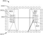
- FIG. 36 is an illustration of a portion of an electronic package according to an embodiment of the invention.
- FIG. 37 is an illustration of the electronic package of FIG. 36 .
- Certain embodiments of the present invention relate to half bridge power conversion circuits that employ one or more gallium nitride (GaN) devices. While the present invention can be useful for a wide variety of half bridge circuits, some embodiments of the invention are particularly useful for half bridge circuits designed to operate at high frequencies and/or high efficiencies with integrated driver circuits, integrated level shift circuits, integrated bootstrap capacitor charging circuits, integrated startup circuits and/or hybrid solutions using GaN and silicon devices, as described in more detail below.
- GaN gallium nitride
- circuit 100 may include a pair of complementary power transistors (also referred to herein as switches) that are controlled by one or more control circuits configured to regulate power delivered to a load.
- a high side power transistor is disposed on a high side device along with a portion of the control circuit and a low side power transistor is disposed on a low side device along with a portion of the control circuit, as described in more detail below.
- the integrated half bridge power conversion circuit 100 illustrated in FIG. 1 includes a low side GaN device 103 , a high side GaN device 105 a load 107 , a bootstrap capacitor 110 and other circuit elements, as illustrated and discussed in more detail below. Some embodiments may also have an external controller (not shown in FIG. 1 ) providing one or more inputs to circuit 100 to regulate the operation of the circuit. Circuit 100 is for illustrative purposes only and other variants and configurations are within the scope of this disclosure.
- low side GaN device 103 may have a GaN-based low side circuit 104 that includes a low side power transistor 115 having a low side control gate 117 .
- Low side circuit 104 may further include an integrated low side transistor driver 120 having an output 123 connected to low side transistor control gate 117 .
- side GaN device 105 may have a GaN-based high side circuit 106 that includes a high side power transistor 125 having a high side control gate 127 .
- High side circuit 106 may further include an integrated high side transistor driver 130 having an output 133 connected to high side transistor control gate 127 .
- a voltage source 135 (also known as a rail voltage) may be connected to a drain 137 of high side transistor 125 , and the high side transistor may be used to control power input into power conversion circuit 100 .
- High side transistor 125 may further have a source 140 that is coupled to a drain 143 of low side transistor 115 , forming a switch node 145 .
- Low side transistor 115 may have a source 147 connected to ground.
- low side transistor 115 and high side transistor 125 may be GaN-based enhancement-mode field effect transistors.
- low side transistor 115 and high side transistor 125 may be any other type of device including, but not limited to, GaN-based depletion-mode transistors, GaN-based depletion-mode transistors connected in series with silicon based enhancement-mode field-effect transistors having the gate of the depletion-mode transistor connected to the source of the silicon-based enhancement-mode transistor, silicon carbide based transistors or silicon-based transistors.
- high side device 105 and low side device 103 may be made from a GaN-based material.
- the GaN-based material may include a layer of GaN on a layer of silicon.
- the GaN based material may include, but not limited to, a layer of GaN on a layer of silicon carbide, sapphire or aluminum nitride.
- the GaN based layer may include, but not limited to, a composite stack of other III nitrides such as aluminum nitride and indium nitride and III nitride alloys such as AlGaN and InGaN.
- GaN-based low side circuit 104 and GaN-based high side circuit 106 may be disposed on a monolithic GaN-based device. In other embodiments GaN-based low side circuit 104 may be disposed on a first GaN-based device and GaN-based high side circuit 106 may be disposed on a second GaN-based device. In yet further embodiments GaN-based low side circuit 104 and GaN-based high side circuit 106 may be disposed on more than two GaN-based devices. In one embodiment, GaN-based low side circuit 104 and GaN-based high side circuit 106 may contain any number of active or passive circuit elements arranged in any configuration.
- Low side device 103 may include numerous circuits used for the control and operation of the low side device and high side device 105 .
- low side device 103 may include logic, control and level shift circuits (low side control circuit) 150 that controls the switching of low side transistor 115 and high side transistor 125 along with other functions, as discussed in more detail below.
- Low side device 103 may also include a startup circuit 155 , a bootstrap capacitor charging circuit 157 and a shield capacitor 160 , as also discussed in more detail below.
- low side control circuit 150 the circuits within low side control circuit 150 are functionally illustrated. Each circuit within low side control circuit 150 is discussed below, and in some cases is shown in more detail in FIGS. 3 - 14 .
- the primary function of low side control circuit 150 may be to receive one or more input signals, such as a PWM signal from a controller, and control the operation of low side transistor 115 , and high side transistor 125 .
- first and a second level shift transistors 203 , 205 may be employed to communicate with high side logic and control circuit 153 (see FIG. 1 ).
- first level shift transistor 203 may be a high voltage enhancement-mode GaN transistor.
- first level shift transistor 203 may be similar to low side transistor 115 (see FIG. 1 ) and high side transistor 125 , except it may be much smaller in size (e.g., first level shift transistor may be tens of microns in gate width with minimum channel length).
- first level shift transistor 203 may experience high voltage and high current at the same time (i.e. the device may operate at the high power portion of the device Safe Operating Area) for as long as high side transistor 125 (see FIG. 1 ) is on. Such conditions may cause relatively high power dissipation, thus some embodiments may involve design and device reliability considerations in the design of first level shift transistor 203 , as discussed in more detail below.
- a first level shift resistor 207 may be added in series with a source 210 of first level shift transistor 203 to limit gate 213 to source 210 voltage and consequently the maximum current through the first level shift transistor. Other methods may be employed to limit the current through first level shift transistor 203 , and are within the scope of this disclosure. Drain 215 of first level shift transistor 203 may be coupled to high side logic and control circuit 153 (see FIG. 1 ), as discussed in more detail below.
- first level shift transistor 203 may comprise a portion of an inverter circuit having a first input and a first output and configured to receive a first input logic signal at the first input terminal and in response, provide a first inverted output logic signal at the first output terminal, as discussed in more detail below.
- first input and the first inverted output logic signals can be referenced to different voltage potentials.
- first level shift resistor 207 may be capable of operating with the first inverted output logic signal referenced to a voltage that is more than 13 volts higher than a reference voltage for the first input logic signal. In other embodiments it may be capable of operating with the first inverted output logic signal referenced to a voltage that is more than 20 volts higher than a reference voltage for the first input logic signal, while in other embodiments it may be between 80-400 volts higher.
- first level shift resistor 207 may be replaced by any form of a current sink.
- source 210 of first level shift transistor 203 may be connected to a gate to source shorted depletion-mode device.
- the depletion-mode device may be fabricated by replacing the enhancement-mode gate stack with a high voltage field plate metal superimposed on top of the field dielectric layers. The thickness of the field dielectric and the work function of the metal may be used to determine the pinch-off voltage of the stack.
- first level shift resistor 207 may be replaced by a current sink.
- the current sink may use a reference current (Iref) that may be generated by startup circuit 155 (illustrated in FIG. 1 and discussed in more detail below).
- Iref reference current
- Both the depletion-mode transistor and current sink embodiments may result in a significant device area reduction compared to the resistor embodiment (i.e., because a relatively small depletion-mode transistor would suffice and Iref is already available from startup circuit 155 ).
- Second level shift transistor 205 may be designed similar to first level shift transistor 203 (e.g., in terms of voltage capability, current handling capability, thermal resistance, etc.). Second level shift transistor 205 may also be built with either an active current sink or a resistor, similar to first level shift transistor 203 . In one embodiment the primary difference with second level shift transistor 205 may be in its operation. In some embodiments the primary purpose of second level shift transistor 205 may be to prevent false triggering of high side transistor 125 (see FIG. 1 ) when low side transistor 115 turns off.
- false triggering can occur in a boost operation when low side transistor 115 turn off results in the load current flowing through high side transistor 125 while the transistor is operating in the third quadrant with its gate shorted to its source (i.e., in synchronous rectification mode).
- This condition may introduce a dv/dt condition at switch node (Vsw) 145 since the switch node was at a voltage close to ground when low side transistor 115 was on and then transitions to rail voltage 135 over a relatively short time period.
- first level shift node 305 see FIG.
- this condition may not be desirable because there may be no dead time control, and shoot through may occur from high side transistor 125 and low side transistor 115 being in a conductive state simultaneously.
- FIG. 3 illustrates one embodiment showing how first level shift transistor 203 may be electrically coupled to high side device 105 .
- First level shift transistor 203 located on low side device 103 , is illustrated along with a pull up resistor 303 that may be located on high side device 105 (see FIG. 1 ).
- first level shift transistor 203 may operate as a pull down transistor in a resistor pull up inverter.
- level shift driver circuit 217 when level shift driver circuit 217 (see FIG. 2 ) supplies a high gate signal (L 1 _DR) to first level shift transistor 203 , a first level shift node 305 gets pulled low which is inverted by high side logic and control circuit 153 (see FIG. 1 ). The inverted signal appears as a high state signal that turns on high side transistor 137 (see FIG. 1 ) which then pulls the voltage at switch node (Vsw) 145 close to rail voltage 135 .
- Vsw switch node
- first level shift transistor 203 when level shift driver circuit 217 (see FIG. 2 ) supplies a low gate signal to first level shift transistor 203 , a first level shift node 305 gets pulled to a high logic state which is inverted by high side logic and control circuit 153 (see FIG. 1 ). The inverted signal appears as a low logic state signal that turns off high side transistor 125 . This scheme may result in a non-inverted gate signal to high side transistor 125 .
- first level shift transistor 203 may be designed large enough to be able to pull down on first level shift node 305 , but not so large that its drain to source and drain to substrate (i.e., the semiconductor substrate) capacitances induce false triggering of high side logic and control circuit 153 .
- pull up resistor 303 may instead be an enhancement-mode transistor, a depletion-mode transistor or a reference current source element.
- pull up resistor 303 may be coupled between the drain and the positive terminal of a floating supply (e.g., a bootstrap capacitor, discussed in more detail below) that is referenced to a different voltage rail than ground.
- a floating supply e.g., a bootstrap capacitor, discussed in more detail below
- the first capacitance may be designed such that in response to a high dv/dt signal at switch node (Vsw) 145 (see FIG. 1 ), a large portion of the C*dv/dt current is allowed to conduct through the first capacitance ensuring that the voltage at first output terminal 305 tracks the voltage at the switch node (Vsw).
- shield capacitor 160 (see FIG. 1 ) may be designed to act as the first capacitor as described above.
- shield capacitor 160 may be used to create capacitance between first output terminal 305 and switch node (Vsw) 145 (see FIG. 1 ) in half bridge power conversion circuit 100 .
- shield capacitor 160 see FIG.
- shield capacitor 160 may be created by adding a conductive shield layer to the device and coupling the layer to switch node (Vsw) 145 . This structure may effectively create two capacitors. One capacitor is coupled between output terminal 305 and switch node (Vsw) 145 , and the other is coupled between the switch node and the substrate. The capacitance between output terminal 305 and the substrate is thereby practically eliminated.
- shield capacitor 160 (see FIG. 1 ) may be constructed on the low side chip 103 .
- Logic, control and level shifting circuit 150 may have other functions and circuits such as, but not limited to, a level shift driver circuit 217 , a low side transistor drive circuit 120 , a blanking pulse generator 223 , a bootstrap transistor drive circuit 225 and an under voltage lock out (UVLO) circuit 227 , as explained in separate figures with more detail below.
- a level shift driver circuit 217 may have other functions and circuits such as, but not limited to, a level shift driver circuit 217 , a low side transistor drive circuit 120 , a blanking pulse generator 223 , a bootstrap transistor drive circuit 225 and an under voltage lock out (UVLO) circuit 227 , as explained in separate figures with more detail below.
- UVLO under voltage lock out
- level shift driver circuit 217 may include a first inverter 405 and a second inverter 410 in a sequential chain. In further embodiments, since level shift driver circuit 217 may be driving a small gate width first level shift transistor 203 , there may be no need for a buffer stage.
- level shift driver circuit 217 is driven directly by the pulse-width modulated high side signal (PWM_HS) from the controller (not shown).
- the (PWM_HS) signal may be supplied by an external control circuit.
- the external control circuit may be an external controller that is in the same package with high side device 105 , low side device 103 , both devices, or packaged on its own.
- level shift driver circuit 217 may also include logic that controls when the level shift driver circuit communicates with first level shift transistor 203 (see FIG. 3 ).
- an optional low side under voltage lock out signal (LS_UVLO) may be generated by an under voltage lock out circuit within level shift driver circuit 217 . The low side under voltage lock out circuit can be used to turn off level shift driver circuit 217 if either (Vcc) or (Vdd) for the low side (Vdd_LS) go below a certain reference voltage, or a fraction of the reference voltage.
- level shift driver circuit 217 may generate a shoot through protection signal for the low side transistor (STP_LS) that is used to prevent shoot through arising from overlapping gate signals on low side transistor 115 and high side transistor 125 .
- the function of the (STP_LS) signal may be to ensure that low side driver circuit 120 (see FIG. 2 ) only communicates with the gate terminal of the low side transistor 115 when the gate signal to high side transistor 125 is low.
- the output of first inverter 405 may be used to generate the shoot through protection signal (STP_LS) for the low side transistor 115 .
- logic for UVLO and shoot-through protection may implemented by adding a multiple input NAND gate to first inverter 405 , where the inputs to the NAND gate are the (PWM_HS), (LS_UVLO) and (STP_HS) signals.
- first inverter 405 may only respond to the (PWM_HS) signal if both (STP_HS) and (LS_UVLO) signals are high.
- the STP_HS signal may be generated from the low side gate driver block 120 , as explained in separate figures with more detail.
- blanking pulse generator 223 may be used to generate a pulse signal that corresponds to the turn off transient of low side transistor 115 .
- This pulse signal may then turn on second level shift transistor 205 for the duration of the pulse, which triggers a control circuit on high side device 105 (see FIG. 1 ) to prevent false pull down of first level shift node 305 voltage.
- FIG. 5 illustrates a schematic of one embodiment of blanking pulse generator 223 .
- a low side transistor 115 gate signal (LS_GATE) is fed as an input to blanking pulse generator 223 .
- the (LS_GATE) signal is inverted by a first stage inverter 505 , then sent through an RC pulse generator 510 to generate a positive pulse.
- an inverted signal may be needed because the pulse corresponds to the falling edge of the (LS_GATE) signal.
- a capacitor 515 in RC pulse generator 510 circuit may be used as a high pass filter allowing the dv/dt at its input to appear across resistor 520 .
- capacitor 515 may charge slowly through resistor 520 , resulting in a slow decaying voltage waveform across the resistor.
- the pulse may then be sent through a second inverter 525 , a third inverter 530 and a buffer 535 to generate a square wave pulse for the blanking pulse (B_PULSE) signal.
- the duration of the pulse may be determined by the value of capacitor 515 and resistor 520 in RC pulse generator 510 .
- capacitor 515 may be constructed using a drain to source shorted enhancement-mode GaN transistor.
- example waveforms 600 within blanking pulse generator 223 are illustrated for one embodiment.
- Trace 605 shows a falling edge of the low side gate pulse (LS_GATE).
- Trace 610 shows the rising edge of first stage inverter 505 output.
- Trace 615 shows the output of RC pulse generator 510 and trace 620 shows the resulting blanking pulse (B_PULSE) signal that is an output of blanking pulse generator 223 .
- Bootstrap transistor drive circuit 225 includes inverter 730 , first buffer 735 and second buffer 745 .
- Bootstrap transistor drive circuit 225 may receive the (BOOTFET_DR_IN) signal from low side driver circuit 120 .
- the (BOOTFET_DR_IN) signal may be inverted with respect to the LS_GATE signal.
- Bootstrap transistor drive circuit 225 may be configured to provide a gate drive signal called (BOOTFET_DR) to a bootstrap transistor in bootstrap charging circuit 157 (see FIG. 1 ), discussed in more detail below.
- the (BOOTFET_DR) gate drive signal may be timed to turn on the bootstrap transistor when low side transistor 115 is turned on.
- bootstrap transistor drive circuit 225 is driven by (Vcc)
- the output of this circuit may have a voltage that goes from 0 volts in a low state to (Vcc)+6 volts in a high state.
- the bootstrap transistor is turned on after low side transistor 115 is turned on, and the bootstrap transistor is turned off before the low side transistor is turned off.
- the turn on transient of the (BOOTFET_DR) signal may be delayed by the introduction of a series delay resistor 705 to the input of second buffer 745 , that may be a gate of a transistor in a final buffer stage.
- the turn off transient of low side transistor 115 may be delayed by the addition of a series resistor to a gate of a final pull down transistor in low side drive circuit 120 .
- one or more capacitors may be used in bootstrap transistor drive circuit 225 , and support voltages of the order of (Vcc) which, for example, could be 20 volts, depending on the end user requirements and the design of the circuit.
- the one or more capacitors may be made with a field dielectric to GaN capacitor instead of a drain to source shorted enhancement-mode transistor.
- Low side transistor drive circuit 120 may have a first inverter 805 , a buffer 810 , a second inverter 815 , a second buffer 820 and a third buffer 825 .
- Third buffer 825 may provide the (LS_GATE) signal to low side transistor 115 (see FIG. 1 ).
- two inverter/buffer stages may be used because the input to the gate of low side transistor 115 (see FIG. 1 ) may be synchronous with (Vin).
- (Vin) in a high state may correspond to (Vgate) of low side transistor 115 in a high state and vice versa.
- certain portions of low side drive circuit 120 may have an asymmetric hysteresis.
- Some embodiments may include asymmetric hysteresis using a resistor divider 840 with a transistor pull down 850 .
- low side drive circuit 120 may receive the shoot through protection signal (STP_LS) from level shift driver circuit 217 .
- the purpose of the (STP_LS) signal may be similar to the (STP_HS) signal described previously.
- the (STP_LS) signal may ensure that low side transistor drive circuit 120 does not communicate with gate 117 (see FIG. 1 ) of low side transistor 115 when level shift driver circuit 217 output is at a high state.
- the output of the first inverter stage 805 may be used as the (STP_HS) signal for level shift drive circuit 217 and the (BOOTFET_DR_IN) signal for bootstrap transistor drive circuit 225 .
- low side transistor drive circuit 120 may employ multiple input NAND gates for the (LS_UVLO) signal received from UVLO circuit 227 (see FIG. 2 ). Further embodiments may employ a turn off delay resistor that may be in series with a gate of a final pull down transistor in final buffer stage 825 . The delay resistor may be used in some embodiments to make sure the bootstrap transistor is turned off before low side transistor 115 turns off.
- startup circuit 155 may be designed to have a multitude of functionalities as discussed in more detail below.
- startup circuit 155 may be used to provide an internal voltage (in this case START_Vcc) and provide enough current to support the circuits that are being driven by (Vcc). This voltage may remain on to support the circuits until (Vcc) is charged up to the required voltage externally from rail voltage 135 (V+).
- Startup circuit 155 may also provide a reference voltage (Vref) that may be independent of the startup voltage, and a reference current sink (Iref).
- a depletion-mode transistor 905 may act as the primary current source in the circuit.
- depletion-mode transistor 905 may be formed by a metal layer disposed over a passivation layer.
- depletion-mode transistor 905 may use a high voltage field plate (typically intrinsic to any high-voltage GaN technology) as the gate metal.
- a field dielectric may act as the gate insulator.
- the resultant gated transistor may be a depletion-mode device with a high channel pinch-off voltage (Vpinch) (i.e., pinch-off voltage is proportional to the field dielectric thickness).
- Vpinch pinch-off voltage
- Depletion-mode transistor 905 may be designed to block relatively high voltages between its drain (connected to V+) and its source. Such a connection may be known as a source follower connection. Depletion-mode transistor 905 may have a gate 906 coupled to ground, a source 907 coupled to a first node 911 and a drain 909 coupled to voltage source 135 .
- a series of identical diode connected enhancement-mode low-voltage transistors 910 may be in series with depletion-mode transistor 905 .
- Series of identical diode connected enhancement-mode low-voltage transistors 910 may be connected in series between a first node 911 and a second node 912 .
- One or more intermediate nodes 913 may be disposed between each of series of identical diode connected enhancement-mode low-voltage transistors 910 .
- the width to length ratio of the transistors may set the current drawn from (V+) as well as the voltage across each diode.
- series of identical diode connected enhancement-mode low-voltage transistors 910 may be designed as large channel length devices.
- series of identical diode connected enhancement-mode low-voltage transistors 910 may be replaced with one or more high value resistors.
- a current mirror 915 may be constructed from two enhancement-mode low-voltage transistors and used to generate a reference current sink (Iref).
- First current mirror transistor 920 may be diode connected and second current mirror transistor 925 may have a gate connected to the gate of the first current mirror transistor.
- the sources of first and second current mirror transistors 920 , 925 respectively may be coupled and tied to ground.
- a drain terminal of first current mirror transistor 920 may be coupled to second junction 912 and a source terminal of second current mirror transistor 925 may be used as a current sink terminal.
- This stack of current mirror 915 and series of identical diode connected enhancement-mode low-voltage transistors 910 may form what is known as a “source follower load” to depletion-mode transistor 905 .
- source 907 of the depletion-mode transistor may assume a voltage close to (Vpinch) when current is supplied to the “source follower load”.
- Vpinch the voltage drop across diode connected transistor 920 in current mirror 915 may be close to the threshold voltage of the transistor (Vth).
- Vth the threshold voltage of the transistor
- (Vpinch) 40 volts
- startup circuit 155 may generate a reference voltage signal (Vref).
- Vref reference voltage signal
- the circuit that generates (Vref) may be similar to the startup voltage generation circuit discussed above.
- a disable pull down transistor 935 may be connected across the gate to source of startup transistor 930 .
- startup transistor 930 When the disable signal is high, startup transistor 930 will be disabled.
- a pull down resistor 940 may be connected to the gate of disable transistor 935 to prevent false turn on of the disable transistor.
- a diode clamp 945 may be connected between the gate and the source terminals of startup transistor 930 to ensure that the gate to source voltage capabilities of the startup transistor are not violated during circuit operation (i.e., configured as gate overvoltage protection devices).
- diode clamp 945 may be made with a series of diode connected GaN-based enhancement-mode transistors 1050 , as illustrated in FIG. 10 .
- UVLO circuit 227 may have a differential comparator 1105 , a down level shifter 1110 and an inverter 1115 .
- UVLO circuit 227 may use (Vref) and (Iref) generated by startup circuit 155 (see FIG. 9 ) in a differential comparator/down level shifter circuit to generate the (LS_UVLO) signal that feeds into level shift driver circuit 217 (see FIG. 2 ) and low side transistor driver circuit 120 .
- UVLO circuit 227 can also be designed to have asymmetric hysteresis.
- the output of UVLO circuit 227 may be independent of threshold voltage.
- the gain can be increased by increasing the value of the current source and the pull up resistors in the differential comparator.
- the limit on the current and resistor may be set by (Vref).
- voltages (VA) and (VB), 1120 and 1125 may be proportional to (Vcc) or (Vdd_LS) and (Vref) as dictated by the resistor divider ratio on each input.
- Vcc voltages
- Vdd_LS voltages
- Vref voltages
- the output of the inverting terminal goes to a low state.
- the low state (Vth) since the current source creates a source follower configuration.
- (VA) 1120 ⁇ (VB) 1125 the output goes to a high state (Vref).
- down level shifter 1110 may be needed because the low voltage needs to be shifted down by one threshold voltage to ensure that the low input to the next stage is below (Vth).
- the down shifted output may be inverted by a simple resistor pull up inverter 1115 .
- the output of inverter 1115 is the (LS_UVLO) signal.
- bootstrap capacitor charging circuit 157 may include a parallel connection of a high voltage diode connected enhancement-mode transistor 1205 and a high voltage bootstrap transistor 1210 .
- high voltage diode connected enhancement-mode transistor 1205 and high voltage bootstrap transistor 1210 can be designed to share the same drain finger.
- the (BOOTFET_DR) signal may be derived from bootstrap transistor drive circuit 225 (see FIG. 2 ).
- high voltage bootstrap transistor 1210 may be turned on coincident with the turn on of low side transistor 115 (see FIG. 1 ).
- an alternative bootstrap diode and transistor circuit 1300 may be used in place of bootstrap diode and transistor circuit 157 discussed above in FIG. 12 .
- a depletion-mode device 1305 cascoded by an enhancement-mode low voltage GaN device 1310 may be connected as illustrated in schematic 1300 .
- a gate of depletion-mode device 1305 can be connected to ground to reduce the voltage stress on cascoded enhancement-mode device 1310 , depending upon the pinch-off voltage of the depletion-mode device.
- high side logic and control circuit 153 is illustrated in greater detail.
- high side driver 130 receives inputs from first level shift receiver 1410 and high side UVLO circuit 1415 and sends a (HS_GATE) signal to high side transistor 125 (see FIG. 1 ).
- a pull up trigger circuit 1425 is configured to receive the (LSHIFT_ 1 ) signal and control pull up transistor 1435 .
- second level shift receiver circuit 1420 is configured to control blanking transistor 1440 . Both the pull up transistor 1435 and blanking transistor 1440 may be connected in parallel with pull up resistor 1430 .
- Each circuit within high side logic and control circuit 153 is discussed below, and in some cases is shown in more detail in FIGS. 16 - 20 .
- first level shift receiver 1410 may convert the (L_SHIFT 1 ) signal to an (LS_HSG) signal that can be processed by high side transistor driver 130 (see FIG. 14 ) to drive high side transistor 125 (see FIG. 1 ).
- first level shift receiver 1410 may have three enhancement-mode transistors 1505 , 1510 , 1515 employed in a multiple level down shifter and a plurality of diode connected transistors 1520 acting as a diode clamp, as discussed in more detail below.
- first level shift receiver 1410 may down shift the (L_SHIFT 1 ) signal by 3*Vth (e.g., each enhancement-mode transistor 1505 , 1510 , 1515 may have a gate to source voltage close to Vth).
- the last source follower transistor e.g., in this case transistor 1515
- transistor 1515 may have a three diode connected transistor clamp 1520 across its gate to source.
- this arrangement may be used because its source voltage can only be as high as (Vdd_HS) (i.e., because its drain is connected to Vdd_HS) while its gate voltage can be as high as V (L_SHIFT1) ⁇ 2*Vth.
- the maximum gate to source voltage on last source follower transistor 1515 may be greater than the maximum rated gate to source voltage of the device technology.
- the output of final source follower transistor 1515 is the input to high side transistor drive 130 (see FIG. 1 ), (i.e., the output is the LS_HSG signal).
- fewer or more than three source follower transistors may be used.
- fewer or more than three diode connected transistors may be used in clamp 1520 .
- second level shift receiver 1420 may have a down level shift circuit 1605 and an inverter circuit 1610 .
- second level shift receiver 1420 may be constructed in a similar manner as first level shift receiver 1410 (see FIG. 15 ), except the second level shift receiver may have only one down level shifting circuit (e.g., enhancement-mode transistor 1615 ) and a follow on inverter circuit 1610 .
- down level shift circuit 1605 may receive the (L_SHIFT 2 ) signal from second level shift transistor 205 (see FIG. 2 ).
- inverter circuit 1610 may be driven by the (Vboot) signal, and the gate voltage of the pull up transistor of the inverter may be used as the (BLANK_FET) signal driving blanking transistor 1440 (see FIG. 14 ).
- the voltage may go from 0 volts in a low state to (Vboot+0.5*(Vboot ⁇ Vth)) in a high state.
- second level shift receiver 1420 may have a diode connected transistor clamp 1620 across the gate to source of source follower transistor 1615 .
- clamp 1620 may include fewer or more than three diode connected transistors.
- pull up trigger circuit 1425 may have a first inverter 1705 , a second inverter 1710 , an RC pulse generator 1715 and a gate to source clamp 1720 .
- pull up trigger circuit 1425 may receive the (L_SHIFT 1 ) signal as an input, and in response, generate a pulse as soon as the (L_SHIFT 1 ) voltage transitions to approximately the input threshold of first inverter 1705 .
- the generated pulse may be used as the (PULLUP_FET) signal that drives pull up transistor 1435 (see FIG. 14 ).
- Second inverter 1710 may be driven by (Vboot) instead of (Vdd_HS) because pull up transistor 1435 gate voltage may need to be larger than the (L_SHIFT 1 ) signal voltage.
- high side UVLO circuit 1415 may have down level shifter 1805 , a resistor pull up inverter with asymmetric hysteresis 1810 and a gate to source clamp 1815 .
- the (HS_UVLO) signal generated by high side UVLO circuit 1415 may aid in preventing circuit failure by turning off the (HS_GATE) signal generated by high side drive circuit 130 (see FIG. 14 ) when bootstrap capacitor 110 voltage goes below a certain threshold.
- bootstrap capacitor 110 voltage (i.e., a floating power supply voltage) is measured, and in response, a logic signal is generated and combined with the output signal (LS_HSG) from first level shift receiver 1410 which is then used as the input to the high side gate drive circuit 130 .
- the UVLO circuit is designed to engage when (Vboot) reduces to less than 4*Vth above switch node (Vsw) 145 voltage. In other embodiments a different threshold level may be used.
- high side UVLO circuit 1415 may down shift (Vboot) in down level shifter 1805 and transfer the signal to inverter with asymmetric hysteresis 1810 .
- the output of inverter with asymmetric hysteresis 1810 may generate the (HS_UVLO) signal which is logically combined with the output from the first level shift receiver 1410 to turn off high side transistor 125 (see FIG. 1 ).
- the hysteresis may be used to reduce the number of self-triggered turn on and turn off events of high side transistor 125 (see FIG. 1 ), that may be detrimental to the overall performance of half bridge circuit 100 .
- High side transistor driver 130 may have a first inverter stage 1905 followed by a high side drive stage 1910 .
- First inverter stage 1905 may invert the down shifted (LS_HSG) signal received from level shift 1 receiver 1410 (see FIG. 15 ). The downshifted signal may then be sent through high side drive stage 1910 .
- High side drive stage 1910 may generate the (HS_GATE) signal to drive high side transistor 125 (see FIG. 1 ).
- first inverter stage 1905 may contain a two input NOR gate that may ensure high side transistor 125 (see FIG. 1 ) is turned off when the (HS_UVLO) signal is in a high state.
- a reference voltage generation circuit 2000 may be used, to generate a high side reference voltage from a supply rail. Such a circuit maybe placed on the high side GaN device 105 for generating internal power supplies which are referenced to the switch node voltage 145 .
- circuit 2000 may be similar to startup circuit 155 in FIG. 9 .
- One difference in circuit 2000 may be the addition of a source follower capacitor 2010 connected between first node 2011 and second node 2012 .
- source follower capacitor 2010 may be needed to ensure that a well regulated voltage, which does not fluctuate with dv/dt appearing at the switch node (Vsw) 145 , develops between the first node 2011 and the second node 2012 .
- a reference voltage capacitor 2015 may be connected between a source of reference voltage transistor 2055 and second node 2012 .
- the drain of the reference voltage transistor 2055 may be connected to the (Vboot) node.
- reference voltage capacitor 2015 may be needed to ensure that (Vref) is well regulated and does not respond to high dv/dt conditions at switch node (Vsw) 145 (see FIG. 1 ).
- another difference in circuit 2000 may be that second node 2012 may be coupled to a constantly varying voltage, such as switch node (Vsw) 145 (see FIG. 1 ), rather than a ground connection through a current sink circuit 915 (see FIG. 9 ).
- (Vref) can be used as (Vdd_HS) in the half bridge circuit 100 .
- Another difference in circuit 2000 may be the addition of a high-voltage diode connected transistor 2025 (i.e., the gate of the transistor is coupled to the source of the transistor) coupled between depletion-mode transistor 2005 and series of identical diode connected enhancement-mode low-voltage transistors 2020 .
- high-voltage diode connected transistor 2025 may have source coupled to the source of depletion-mode transistor 2005 , a drain coupled to first node 2011 and a gate coupled to its source.
- High-voltage diode connected transistor 2025 may be used to ensure that source follower capacitor 2010 does not discharge when the voltage at the top plate of the source follower capacitor rises above (V+).
- source follower capacitor 2010 may be relatively small and may be integrated on a semiconductor substrate or within an electronic package.
- bootstrap capacitor 110 that may be added externally in a half bridge circuit.
- shield capacitor 160 may be connected from first level shift node 305 (see FIG. 3 ) and second level shift node (not shown) to switch node 145 to assist in reducing the false triggering discussed above.
- the larger the value of shield capacitor 160 the more immune the circuit will be to false triggering effects due to the parasitic capacitance to ground.
- shield capacitor 160 may be discharged through pull up resistor 303 (see FIG. 3 ) connected to first level shift node 305 . This may significantly slow down high side transistor 125 turn off process. In some embodiments this consideration may be used to set an upper limit on the value of shield capacitor 160 .
- an overvoltage condition on first level shift node 305 may be prevented by the use of a clamp circuit 161 (see FIG. 1 ) between the first level shift node and switch node 145 .
- clamp circuit 161 maybe composed of a diode connected transistor where a drain of the transistor is connected to first level shift node 305 (see FIG. 3 ) and a gate and a source are connected to switch node (Vsw) 145 (see FIG. 1 ).
- a second shield capacitor and a second clamp circuit may be placed between the second level shift node and switch node (Vsw) 145 (see FIG. 1 ).
- low side logic, control and level shift circuit 150 sends a high signal to low side transistor driver 120 .
- Low side transistor driver 120 then communicates through the (LS_GATE) signal to low side transistor 115 to turn it on. This will set the switch node voltage (Vsw) 145 close to 0 volts.
- Vsw switch node voltage
- the charging path has a parallel combination of a high voltage bootstrap diode 1205 (see FIG. 12 ) and transistor 1210 .
- the (BOOTFET_DR) signal provides a drive signal to bootstrap transistor 1210 (see FIG. 12 ) that provides a low resistance path for charging bootstrap capacitor 110 .
- Bootstrap diode 1205 may be used to ensure that there is a path for charging bootstrap capacitor 110 during startup when there is no low side transistor 115 gate drive signal (LS_GATE). During this time the (PWM_HS) signal should be low. If the (PWM_HS) signal is inadvertently turned on (i.e., in a high state) during this time the (STP_HS) signal generated from low side transistor driver 120 will prevent high side transistor 125 from turning on. If the (PWM_LS) signal is turned on while the (PWM_HS) signal is on, the (STP_LS) signal generated from level shift driver circuit 217 will prevent low side transistor 115 from turning on. Also, in some embodiments the (LS_UVLO) signal may prevent low side transistor 115 and high side transistor 125 from turning on when either (Vcc) or (Vdd_LS) goes below a preset threshold voltage level.
- low side gate signal (LS_GATE) to low side transistor 115 is also low.
- LS_GATE low side gate signal
- an inductive load will force either high side transistor 125 or low side transistor 115 to turn on in the synchronous rectifier mode, depending on direction of power flow. If high side transistor 125 turns on during the dead time (e.g., during boost mode operation), switch node (Vsw) 145 voltage may rise close to (V+) 135 (rail voltage).
- a dv/dt condition on switch node 145 may tend to pull first level shift node (LSHIFT_ 1 ) 305 (see FIG. 3 ) to a low state relative to switch node (Vsw) 145 , due to capacitive coupling to ground. This may turn on high side gate drive circuit 130 causing unintended triggering of high side transistor 125 . In one embodiment, this may result in no dead time which may harm half bridge circuit 100 with a shoot through condition. In further embodiments, to prevent this condition from occurring, blanking pulse generator 223 may sense the turn off transient of low side transistor 115 and send a pulse to turn on second level shift transistor 205 .
- Blanking transistor 1440 may then act as a pull up to prevent first level shift node (LSHIFT_ 1 ) 305 (see FIG. 3 ) from going to a low state relative to switch node (Vsw) 145 .
- level shift driver circuit 217 may send a high signal to the gate of first level shift transistor 203 (via the L 1 _DR signal from level shift driver circuit 217 ).
- the high signal will pull first level shift node (LSHIFT_ 1 ) 305 (see FIG. 3 ) low relative to switch node (Vsw) 145 which will result in a high signal at the input of high side transistor 125 , turning on high side transistor 125 .
- Switch node voltage (Vsw) 145 will remain close to (V+) 135 .
- bootstrap capacitor 110 may discharge through first level shift transistor 203 (which is in an on state during this time).
- bootstrap capacitor 110 voltage will go down to a low enough voltage that it will prevent high side transistor 125 from turning off when the (PWM_HS) signal goes low. In some embodiments this may occur because the maximum voltage the (L_SHIFT 1 ) signal can reach is (Vboot) which may be too low to turn off high side transistor 125 . In some embodiments, this situation may be prevented by high side UVLO circuit 1415 that forcibly turns off high side transistor 125 by sending a high input to high side gate drive circuit 130 when (Vboot) goes below a certain level.
- first level shift transistor 203 when the (PWM_HS) signal goes low, first level shift transistor 203 will also turn off (via the L 1 _DR signal from the level shift driver circuit 217 ). This will pull first level shift node (LSHIFT_ 1 ) 305 (see FIG. 3 ) to a high state.
- this process may be relatively slow because the high value pull up resistor 303 (see FIG. 3 ) (used to reduce power consumption in some embodiments) needs to charge all the capacitances attached to first level shift node (L_SHIFT 1 ) 305 (see FIG. 3 ) including the output capacitance (Coss) of first level shift transistor 213 and shield capacitor 160 . This may increase the turn off delay of high side transistor 125 .
- pull up trigger circuit 1425 may be used to sense when first level shift node (L_SHIFT 1 ) 305 (see FIG. 3 ) goes above (Vth). This condition may generate a (PULLUP_FET) signal that is applied to pull up transistor 1435 which, acting in parallel with pull up resistor 1430 , may considerably speed up the pull up of first level shift node (L_SHIFT 1 ) 305 (see FIG. 3 ) voltage, hastening the turn off process.
- PLLUP_FET first level shift node
- Half bridge circuit 2100 may have the same block diagram as circuit 100 illustrated in FIG. 1 , however the level shift transistors in circuit 2100 may operate with pulsed inputs, rather than a continuous signal, as described in more detail below.
- pulsed inputs may result in lower power dissipation, reduced stress on the level shift transistors and reduced switching time, as discussed in more detail below.
- one embodiment includes an integrated half bridge power conversion circuit 2100 employing a low side GaN device 2103 , a high side GaN device 2105 , a load 2107 , a bootstrap capacitor 2110 and other circuit elements, as discussed in more detail below. Some embodiments may also have an external controller (not shown in FIG. 21 ) providing one or more inputs to circuit 2100 to regulate the operation of the circuit. Circuit 2100 is for illustrative purposes only and other variants and configurations are within the scope of this disclosure.
- integrated half bridge power conversion circuit 2100 may include a low side circuit disposed on low side GaN device 2103 that includes a low side transistor 2115 having a low side control gate 2117 .
- the low side circuit may further include an integrated low side transistor driver 2120 having an output 2123 connected to a low side transistor control gate 2117 .
- the high side circuit may further include an integrated high side transistor driver 2130 having an output 2133 connected to high side transistor control gate 2127 .
- High side transistor 2125 may be used to control the power input into power conversion circuit 2100 and have a voltage source (V+) 2135 (sometimes called a rail voltage) connected to a drain 2137 of the high side transistor. High side transistor 2125 may further have a source 2140 that is coupled to a drain 2143 of low side transistor 2115 , forming a switch node (Vsw) 2145 . Low side transistor 2115 may have a source 2147 connected to ground. In one embodiment, low side transistor 2115 and high side transistor 2125 may be enhancement-mode field-effect transistors.
- low side transistor 2115 and high side transistor 2125 may be any other type of device including, but not limited to, GaN-based depletion-mode transistors, GaN-based depletion-mode transistors connected in series with silicon based enhancement-mode field-effect transistors having the gate of the depletion-mode transistor connected to the source of the silicon-based enhancement-mode transistor, silicon carbide based transistors or silicon-based transistors.
- high side device 2105 and low side device 2103 may be made from a GaN-based material.
- the GaN-based material may include a layer of GaN on a layer of silicon.
- the GaN based material may include, but not limited to, a layer of GaN on a layer of silicon carbide, sapphire or aluminum nitride.
- the GaN based layer may include, but not limited to, a composite stack of other III nitrides such as aluminum nitride and indium nitride and III nitride alloys such as AlGaN and InGaN
- Low side device 2103 may have numerous circuits used for the control and operation of the low side device and high side device 2105 .
- low side device 2103 may include a low side logic, control and level shift circuit (low side control circuit) 2150 that controls the switching of low side transistor 2115 and high side transistor 2125 along with other functions, as discussed in more detail below.
- Low side device 2103 may also include a startup circuit 2155 , a bootstrap capacitor charging circuit 2157 and a shield capacitor 2160 , as also discussed in more detail below.
- low side control circuit 2150 the circuits within low side control circuit 2150 are functionally illustrated. Each circuit within low side control circuit 2150 is discussed below, and in some cases is shown in more detail in FIGS. 23 - 28 .
- the primary function of low side control circuit 2150 may be to receive one or more input signals, such as a PWM signal from a controller, and control the operation of low side transistor 2115 , and high side transistor 2125 .
- First level shift transistor 2203 may be an “on” pulse level shift transistor, while second level shift transistor 2215 may be an “off” pulse level shift transistor.
- a pulse width modulated high side (PWM_HS) signal from a controller may be processed by inverter/buffer 2250 and sent on to an on pulse generator 2260 and an off pulse generator 2270 .
- On pulse generator 2260 may generate a pulse that corresponds to a low state to high state transient of the (PWM_HS) signal, thus turning on first level shift transistor 2203 during the duration of the pulse.
- Off pulse generator 2270 may similarly generate a pulse that corresponds to the high state to low state transition of the (PWM_HS) signal, thus turning on second level shift transistor 2205 for the duration of the off pulse.
- First and second level shift transistors 2203 , 2205 may operate as pull down transistors in resistor pull up inverter circuits. More specifically, turning on may mean the respective level shift node voltages get pulled low relative to switch node (Vsw) 2145 voltage, and turning off may result in the respective level shift nodes assuming the (Vboot) voltage. Since first and second level shift transistors 2203 , 2215 , respectively, are “on” only for the duration of the pulse, the power dissipation and stress level on these two devices may be less than half bridge circuit 100 illustrated in FIG. 1 .
- First and second resistors 2207 , 2208 may be added in series with the sources of first and second level shift transistors 2203 , 2215 , respectively to limit the gate to source voltage and consequently the maximum current through the transistors.
- First and second resistors 2207 , 2208 could be smaller than the source follower resistors in half bridge circuit 100 illustrated in FIG. 1 , which may help make the pull down action of first and second level shift transistors 2203 , 2215 faster, reducing the propagation delays to high side transistor 2125 .
- first and second resistors 2207 , 2208 could be replaced by any form of a current sink.
- One embodiment may connect the source of first and second level shift transistors 2203 , 2205 , respectively to a gate to source shorted depletion-mode device.
- One embodiment of a depletion-mode transistor formed in a high-voltage GaN technology may be to replace the enhancement-mode gate stack with one of the high-voltage field plate metals superimposed on top of the field dielectric layers. The thickness of the field dielectric and the work function of the metal may control the pinch-off voltage of the stack.
- first and second resistors 2207 , 2208 may be replaced by a current sink.
- a reference current (Iref) that is generated by startup circuit 2155 (see FIG. 21 ) may be used. Both the depletion-mode transistor and current sink embodiments may result in a significant die area reduction compared to the resistor option (i.e., because a small depletion transistor would suffice and Iref is already available).
- Bootstrap transistor drive circuit 2225 may be similar to bootstrap transistor drive circuit 225 illustrated in FIG. 2 above. Bootstrap transistor drive circuit 2225 may receive input from low side drive circuit 2220 (see FIG. 22 ) and provide a gate drive signal called (BOOTFET_DR) to the bootstrap transistor in bootstrap capacitor charging circuit 2157 (see FIG. 21 ), as discussed in more detail above.
- BOOTFET_DR gate drive signal
- first level shift transistor 2203 is illustrated along with a pull up resistor 2303 that may be located in high side device 2105 .
- first level shift transistor 2203 may operate as a pull down transistor in a resistor pull up inverter similar to first level shift transistor 203 illustrated in FIG. 3 .
- pull up resistor 2303 may be disposed in high side device 2105 (see FIG. 21 ).
- Second level shift transistor 2215 may have a similar configuration. In some embodiments there may be a first capacitance between the first output terminal (LS NODE) 2305 and switch node (Vsw) 2145 (see FIG.
- a shield capacitor 2160 may be configured to act as the first capacitor as described above. In further embodiments shield capacitor 2160 (see FIG.
- shield capacitor 2160 may be used to minimize the capacitance between first output terminal 2305 and a substrate of the semiconductor device. In further embodiments shield capacitor 2160 may be constructed on low side GaN device 2103 .
- inverter/buffer circuit 2250 may have a first inverter stage 2405 and a first buffer stage 2410 .
- inverter/buffer circuit 2250 may be driven directly by the (PWM_HS) signal from the controller (not shown).
- the output of first inverter stage 2405 may be the input signal (PULSE_ON) to on pulse generator 2260 (see FIG. 22 ) while the output of first buffer stage 2410 may be an input signal (PULSE_OFF) to off pulse generator 2270 .
- an optional (LS_UVLO) signal may be generated by sending a signal generated by UVLO circuit 2227 (see FIG. 22 ) in to a NAND gate disposed in first inverter stage 2405 .
- This circuit may be used to turn off the level shift operation if either (Vcc) or (Vdd_LS) go below a certain reference voltage (or a fraction of the reference voltage).
- inverter/buffer circuit 2250 may also generate a shoot through protection signal (STP_LS 1 ) for low side transistor 2115 (see FIG. 21 ) that may be applied to low side transistor gate drive circuit 2120 . This may turn off low side transistor gate drive circuit 2120 (see FIG. 21 ) when the (PWM_HS) signal is high, preventing shoot through.
- STP_LS 1 shoot through protection signal
- pulse generator 2260 may have a first inverter stage 2505 , a first buffer stage 2510 , an RC pulse generator 2515 , a second inverter stage 2520 a third inverter stage 2525 and a third buffer stage 2530 .
- the (PULSE_ON) signal input from inverter/buffer circuit 2250 may be first inverted and then transformed into an on pulse by RC pulse generator 2515 and a square wave generator. The result of this operation is the gate drive signal (LI_DR) that is transmitted to first level shift transistor 2203 (see FIG. 22 ).
- on pulse generator 2260 may comprise one or more logic functions, such as for example, a binary or combinatorial function.
- on pulse generator 2260 may have a multiple input NOR gate for the (STP_HS) signal.
- the (STP_HS) signal may have the same polarity as the (LS_GATE) signal. Therefore, if the (STP_HS) signal is high (corresponding to LS_GATE signal being high) the on pulse may not be generated because first inverter circuit 2505 in FIG. 25 will be pulled low which will deactivate pulse generator 2515 .
- RC pulse generator 2515 may include a clamp diode (not shown).
- the clamp diode may be added to ensure that RC pulse generator 2515 works for very small duty cycles for the (PWM_LS) signal.
- on pulse generator 2260 may be configured to receive input pulses in a range of 2 nanoseconds to 20 microseconds and to transmit pulses of substantially constant duration within the range.
- the clamp diode may turn on and short out a resistor in RC pulse generator 2515 (providing a very small capacitor discharge time) if the voltage across the clamp diode becomes larger than (Vth). This may significantly improve the maximum duty cycle of operation (with respect to the PWM_HS signal) of pulse generator circuit 2260 .
- off pulse generator 2270 may have an RC pulse generator 2603 , a first inverter stage 2605 , a second inverter stage 2610 and a first buffer stage 2615 .
- off pulse generator 2270 may receive an input signal (PULSE_OFF) from inverter/buffer circuit 2250 (see FIG. 22 ) that may be subsequently communicated to RC pulse generator 2603 .
- the pulse from RC pulse generator 2603 is sent through first inverter stage 2605 , second inverter stage 2610 and buffer stage 2615 .
- the pulse may then be sent as the (L 2 _DR) signal to second level shift transistor 2215 (see FIG. 22 ).
- a clamp diode may also be included in off pulse generator 2270 .
- the operating principle may be similar to the operating principle discussed above with regard to on pulse generator 2260 (see FIG. 25 ). Such operating principles may ensure that off pulse generator 2270 operates for very low on times of high side transistor 2125 (see FIG. 21 ) (i.e. the circuit will operate for relatively small duty cycles).
- off pulse generator 2270 may be configured to receive input pulses in a range of 2 nanoseconds to 20 microseconds and to transmit pulses of substantially constant duration within the range.
- an off level shift pulse can be shortened by an on input pulse to enable an off time of less than 50 nanoseconds on high side transistor 2125 .
- RC pulse generator 2603 may include a capacitor connected with a resistor divider network.
- the output from the resistor may be a signal (INV) that is sent to an inverter 2275 (see FIG. 22 ) that generates a shoot through protection signal (STP_LS 2 ) transmitted to low side driver circuit 2220 .
- off pulse generator 2270 may comprise one or more logic functions, such as for example, a binary or combinatorial function.
- the (STP_LS 2 ) signal is sent to a NAND logic circuit within low side driver circuit 2220 , similar to the (STP_LS 1 ) signal.
- these signals may be used to ensure that during the duration of the off pulse signal (PULSE_OFF), low side transistor 2115 (see FIG. 21 ) does not turn on (i.e., because high side transistor 2125 turns off during the off pulse).
- this methodology may be useful to compensate for a turn off propagation delay (i.e., the PULSE_OFF signal may enable shoot through protection), ensuring that low side transistor 2115 will only turn on after high side transistor 2125 gate completely turns off.
- a blanking pulse can be level shifted to high side device 2105 using second level shift transistor 2215 .
- a blanking pulse may be sent into a NOR input into first inverter stage 2605 .
- the blanking pulse may be used to inhibit false triggering due to high dv/dt conditions at switch node Vsw 2145 (see FIG. 20 ).
- no blanking pulse may be used to filter dv/dt induced or other unwanted level shift output pulses.
- blanking pulse generator 2223 may be a more simple design than used in half bridge circuit 100 illustrated in FIG. 1 because the square wave pulse generator is already part of off pulse generator 2270 .
- the (LS_GATE) signal is fed as the input to blanking pulse generator 2223 from low side gate drive circuit 2220 (see FIG. 22 ). This signal may be inverted and then sent through an RC pulse generator to generate a positive going pulse. In some embodiments, an inverted signal may be used because the pulse needs to correspond to the falling edge of the (LS_GATE) signal. The output of this may be used as the blanking pulse input (B_PULSE) to off pulse generator 2270 .
- low side transistor drive circuit 2220 may have a first inverter stage 2805 , a first buffer stage 2810 , a second inverter stage 2815 , a second buffer stage 2820 and a third buffer stage 2825 .
- two inverter/buffer stages may be used because the input to the gate of low side transistor 2115 is synchronous with the (PWM_LS) signal.
- a (PWM_LS) high state may correspond to a (LS_GATE) high state and vice versa.
- low side transistor drive circuit 2220 may also include an asymmetric hysteresis using a resistor divider with a transistor pull down similar to the scheme described in 120 (see FIG. 8 ).
- low side transistor drive circuit 2220 includes multiple input NAND gates for the (STP_LS 1 ) and (STP_LS 2 ) (shoot through prevention on low side transistor 2115 ) signals.
- the (STP_LS 1 ) and (STP_LS 2 ) signals may ensure that low side transistor drive circuit 2220 (see FIG. 22 ) does not communicate with low side transistor 2115 (see FIG. 21 ) when high side transistor 2125 is on. This technique may be used to avoid the possibility of shoot-through.
- NAND gates similar to the ones employed above in FIG. 28 ) for the (LS_UVLO) signal.
- One embodiment may include a turn off delay resistor in series with the gate of the final pull down transistor. This may be used to ensure the bootstrap transistor is turned off before low side transistor 2115 turns off.
- low side device 2103 may also include a startup circuit 2155 , bootstrap capacitor charging circuit 2157 , a shield capacitor 2160 , and a UVLO circuit 2227 that may be similar to startup circuit 155 , bootstrap capacitor charging circuit 157 , shield capacitor 160 and UVLO circuit 227 , respectively, as discussed above.
- high side logic and control circuit 2153 and how it interacts with high side transistor driver 2130 is illustrated in greater detail.
- high side logic and control circuit 2153 may operate in similar ways as high side logic and control circuit 153 , discussed above in FIG. 15 .
- high side logic and control circuit 2153 may operate in different ways, as discussed in more detail below.
- level shift 1 receiver circuit 2910 receives an (L_SHIFT 1 ) signal from first level shift transistor 2203 (see FIG. 22 ) that receives an on pulse at the low state to high state transition of the (PWM_HS) signal, as discussed above.
- level shift 1 receiver circuit 2910 drives a gate of pull up transistor 2960 (e.g., in some embodiments a low-voltage enhancement-mode GaN transistor).
- pull up transistor 2960 may then pull up a state storing capacitor 2955 voltage to a value close to (Vdd_HS) with respect to switch node (Vsw) 2145 voltage.
- state storing capacitor 2955 may be a latching storage logic circuit configured to change state in response to a first pulsed input signal and to change state in response to a second pulsed input signal.
- state storing capacitor 2955 may be replaced by any type of a latching circuit such as, but not limited to an RS flip-flop.
- level shift 2 receiver circuit 2920 may maintain pull down transistor 2965 (e.g., in some embodiments a low-voltage enhancement-mode GaN transistor) in an off state. This may cut off any discharge path for state storing capacitor 2955 .
- state storing capacitor 2955 may have a relatively small charging time constant and a relatively large discharge time constant.
- level shift 2 receiver 2920 may receive an (L_SHIFT 2 ) signal from second level shift transistor 2215 (see FIG. 22 ) that receives an off pulse at the high state to low state transition of the (PWM_HS) signal, as discussed above.
- level shift 2 receiver circuit 2920 drives a gate of pull down transistor 2965 (e.g., in some embodiments a low-voltage enhancement-mode GaN transistor).
- pull down transistor 2965 may then pull down (i.e., discharge) state storing capacitor 2955 voltage to a value close to switch node (Vsw) 2145 , that may consequently turn off high side transistor 2125 through high side transistor driver 2130 .
- first and second shield capacitors 2970 , 2975 may be connected from (L_SHIFT 1 ) and (L_SHIFT 2 ) nodes to help prevent false triggering during high dv/dt conditions at switch node (Vsw) 2145 (see FIG. 21 ).
- level shift 1 receiver 2910 may include a down level shifter 3005 , a first inverter 3010 , a second inverter 3015 , a first buffer 3020 , a third inverter 3025 , a second buffer 3030 and a third buffer 3135 .
- level shift 1 receiver 2910 down shifts (i.e., modulates) the (L_SHIFT 1 ) signal by a voltage of 3*Vth (e.g., using three enhancement-mode transistors where each may have a gate to source voltage close to Vth). In other embodiments a fewer or more downshift transistors may be used.
- the last source follower transistor may have a three diode connected transistor clamp across its gate to its source.
- this configuration may be used because its source voltage can only be as high as (Vdd_HS) (i.e., because its drain is connected to Vdd_HS) while its gate voltage can be as high as V (L_SHIFT 1 ) ⁇ 2*Vth.
- Vdd_HS source voltage
- L_SHIFT 1 gate voltage
- the maximum gate to source voltage on the final source follower transistor can be greater than the maximum rated gate to source voltage in the technology.
- first inverter 3010 may also have a NOR Gate for the high side under voltage lock out using the (UV_LS 1 ) signal generated by high side UVLO circuit 2915 .
- an output of level shift 1 receiver 2910 may be a (PU_FET) signal that is communicated to a gate of pull up transistor 2960 (see FIG. 29 ). This signal may have a voltage that goes from 0 volts in a low state to (Vdd_HS)+(Vdd_HS ⁇ Vth) in a high state. This voltage may remain on for the duration of the on pulse.
- level shift 2 receiver 2920 is illustrated in greater detail.
- level shift 2 receiver 2920 may be similar to level shift 1 receiver 2910 discussed above.
- level shift 2 receiver 2920 may include a blanking pulse generator 3105 , a down level shifter 3110 , a first inverter 3115 , a second inverter 3120 , a first buffer 3125 , an third inverter 3130 , a second buffer 3135 and a third buffer 3140 .
- blanking pulse generator 3105 may be used in addition to a 3*Vth down level shifter 3110 and multiple inverter/buffer stages.
- blanking pulse generator 3105 may be identical to level shift 2 receiver 1520 illustrated in FIG. 17 .
- level shift 2 receiver 2920 may receive (L_SHIFT 2 ) and (UV_LS 2 ) signals and in response, transmit a (PD_FET) signal to pull down transistor 2965 .
- first inverter 3115 may have a two input NAND gate for the (UV_LS 2 ) signal from high side UVLO circuit 2915 (see FIG. 29 ).
- high side UVLO circuit 2915 may include a down level shifter 3205 and a resistor pull up inverter stage 3210 .
- high side UVLO circuit 2915 may be configured to prevent circuit failure by turning off the (HS_GATE) signal to high side transistor 2125 (see FIG. 21 ) when bootstrap capacitor 2110 voltage goes below a certain threshold.
- high side UVLO circuit 2915 is designed to engage when (Vboot) reduces to a value less than 4*Vth below switch node (Vsw) 2145 voltage.
- the output of down level shifter 3205 may be a (UV_LS 2 ) signal transmitted to second level shift receiver 2920 and the output of resistor pull up inverter stage 3210 may be an (UV_LS 1 ) signal that is transmitted to first level shift receiver 2910 .
- high side UVLO circuit 2915 may be different from high side UVLO circuit 1415 for half bridge circuit 100 discussed above in FIGS. 14 and 18 , respectively.
- the (Vboot) signal may be down shifted by 3*Vth and transferred to resistor pull up inverter stage 3210 .
- level shift 2 receiver circuit 2920 controls the turn off process based on high side transistor 2125 (see FIG. 21 )
- directly applying a 3*Vth down shifted output to the NAND gate at the input of level shift 2 receiver circuit 2920 will engage the under voltage lock out.
- level shift 2 receiver circuit 2920 (see FIG. 29 ) tries to keep high side transistor 2125 (see FIG. 21 ) off
- level shift 1 receiver circuit 2910 may try to turn the high side transistor on.
- some embodiments may invert the output of the 3*Vth down shifted signal from high side UVLO circuit 2915 (see FIG. 29 ) and send it to a NOR input on level shift 1 receiver circuit 2910 . This may ensure that level shift 1 receiver circuit 2910 does not interfere with the UVLO induced turn off process.
- high side transistor driver 2130 may include a first inverter 3305 , a first buffer 3310 , a second inverter 3315 , a second buffer 3320 and a third buffer 3325 .
- high side transistor driver 2130 may be a more basic design than high side transistor driver 130 employed in half bridge circuit 100 illustrated in FIG. 1 .
- high side transistor driver 2130 receives an (S CAP) signal from state storage capacitor 2955 (see FIG. 29 ) and delivers a corresponding drive (HS_GATE) signal to high side transistor 2125 (see FIG. 21 ). More specifically, when the (S CAP) signal is in a high state, the (HS_GATE) signal is in a high state and vice versa.
- low side logic, control and level shift circuit 2150 may send a high signal to low side transistor driver 2120 which then communicates that signal to low side transistor 2115 to turn it on. This may set switch node (Vsw) 2145 voltage close to 0 volts.
- Vsw switch node
- when low side transistor 2115 turns on it may provide a path for bootstrap capacitor 2110 to charge.
- the charging path may have a parallel combination of a high-voltage bootstrap diode and transistor.
- bootstrap transistor drive circuit 2225 may provide a drive signal (BOOTFET_DR) to the bootstrap transistor that provides a low resistance path for charging bootstrap capacitor 2110 .
- the bootstrap diode may ensure that there is a path for charging bootstrap capacitor 2110 during startup when there is no low side gate drive signal (LS_GATE).
- LS_GATE low side gate drive signal
- the (PWM_HS) signal should be in a low state. If the (PWM_HS) signal is inadvertently turned on during this time, the (STP_HS) signal generated from low side driver circuit 2220 may prevent high side transistor 2125 from turning on.
- the (PWM_LS) signal is turned on while the (PWM_HS) signal is on, then the (STP_LS 1 ) and (STP_LS 2 ) signals generated from inverter/buffer 2250 and inverter 2275 , respectively will prevent low side transistor 2115 from turning on.
- the (LS_UVLO) signal may prevent low side gate 2117 and high side gate 2127 from turning on when either (Vcc) or (Vdd_LS) go below a predetermined voltage level.
- the (LS_GATE) signal to low side transistor 2115 may also be in a low state.
- the inductive load may force either high side transistor 2125 or low side transistor 2115 to turn on in the synchronous rectifier mode, depending on the direction of power flow. If high side transistor 2125 turns on during the dead time (e.g., in a boost mode), switch node (Vsw) 2145 voltage may rise close to (V+) 2135 (i.e., the rail voltage).
- This dv/dt condition on switch node (Vsw) 2145 may tend to pull the (L_SHIFT 1 ) node to a low state relative to the switch node (i.e., because of capacitive coupling to ground) which may turn on high side transistor driver 2130 causing unintended conduction of high side transistor 2125 .
- This condition may negate the dead time, causing shoot through.
- this condition may be prevented by using blanking pulse generator 2223 to sense the turn off transient of low side transistor 2115 and send a pulse to turn on second level shift transistor 2205 . This may pull the (L_SHIFT 2 ) signal to a low state which may then communicate with level shift 2 receiver circuit 2920 to generate a blanking pulse to drive blanking transistor 2940 . In one embodiment, blanking transistor 2940 may act as a pull up to prevent the (L_SHIFT 1 ) signal from going to a low state relative to switch node (Vsw) 2145 .
- an on pulse may be generated by on pulse generator 2260 .
- This may pull the (L_SHIFT 1 ) node voltage low for a brief period of time.
- this signal may be inverted by level shift 1 receiver circuit 2910 and a brief high signal will be sent to pull up transistor 2960 that will charge state storage capacitor 2955 to a high state. This may result in a corresponding high signal at the input of high side transistor driver 2130 which will turn on high side transistor 2125 .
- Switch node (Vsw) 2145 voltage may remain close to (V+) 2135 (i.e., the rail voltage). State storing capacitor 2955 voltage may remain at a high state during this time because there is no discharge path.
- bootstrap capacitor 2110 may discharge through first level shift transistor 2203 .
- bootstrap capacitor 2110 may not discharge as much as it would if first level shift transistor 2203 was on during the entire duration of the (PWM_HS) signal (as was the case in half bridge circuit 100 in FIG. 1 ). More specifically, in some embodiments this may result in the switching frequency at which the UVLO engages to be a relatively lower value than in half bridge circuit 100 in FIG. 1 .
- an off pulse may be generated by off pulse generator 2270 .
- This may pull the (L_SHIFT 2 ) node voltage low for a brief period of time.
- This signal may be inverted by level shift 2 receiver circuit 2920 and a brief high state signal may be sent to pull down transistor 2965 that will discharge state storing capacitor 2955 to a low state. This will result in a low signal at the input of high side transistor driver 2130 that will turn off high side transistor 2125 .
- state storing capacitor 2955 voltage may remain at a low state during this time because it has no discharge path.
- the turn off process in circuit 2100 since the turn off process in circuit 2100 does not involve charging level shift node capacitors through a high value pull up resistor, the turn off times may be relatively shorter than in half bridge circuit 100 in FIG. 1 .
- high side transistor 2125 turn on and turn off processes may be controlled by the turn on of substantially similar level shift transistors 2203 , 2205 , therefore the turn on and turn off propagation delays may be substantially similar. This may result in embodiments that have no need for a pull up trigger circuit and/or a pull up transistor as were both used in half bridge circuit 100 in FIG. 1 .
- one or more pins may employ an electro-static discharge (ESD) clamp circuit to protect the circuit.
- ESD electro-static discharge
- the following embodiments illustrate ESD clamp circuits that may be used on one or more pins in one or more embodiments disclosed herein, as well as other embodiments that may require ESD protection.
- the ESD clamp circuits disclosed herein may be employed on GaN-based devices.
- ESD clamp circuit 3400 may have a configuration employing one or more source follower stages 3405 made from enhancement-mode transistors. Each source follower stage 3405 may have a gate 3406 connected to a source 3407 of an adjacent source follower stage. In the embodiment illustrated in FIG. 34 , four source follower stages 3405 are employed, however in other embodiments fewer or more may be used. Resistors 3410 are coupled to sources 3407 of source follower stages 3405 .
- An ESD transistor 3415 is coupled to one or more source follower stages 3405 and may be configured to conduct a current greater than 500 mA when exposed to an overvoltage pulse, as discussed below.
- Resistors 3410 are disposed between source 3420 of ESD transistor 3415 and each source 3407 of source follower stages 3405 .
- Drains 3408 of source follower stages 3405 are connected to drain 3425 of ESD transistor 3415 .
- Source 3407 of the last source follower stage is coupled to gate 3430 of ESD transistor 3415 .
- a turn on voltage of ESD clamp circuit 3400 can be set by the total number of source follower stages 3405 .
- the last source follower stage is a transistor with a certain drain 3408 to source 3407 voltage and gate 3406 to source voltage the current through the final resistor 3410 may be relatively large and may result in a larger gate 3430 to source 3420 voltage across ESD transistor 3415 . This condition may result in a relatively large ESD current capability and in some embodiments an improved leakage performance compared to other ESD circuit configurations.
- ESD clamp circuit 3400 may have a plurality of degrees of freedom with regard to transistor sizes and resistor values. In some embodiments ESD clamp circuit 3400 may be able to be made smaller than other ESD circuit configurations. In other embodiments, the performance of ESD clamp circuit 3400 may be improved by incrementally increasing the size of source follower stages 3405 as they get closer to ESD transistor 3415 . In further embodiments, resistors 3410 can be replaced by depletion-mode transistors, reference current sinks or reference current sources, for example.
- ESD clamp circuit 3500 may have resistors in a different configuration, as discussed in more detail below.
- ESD clamp circuit 3500 may have a configuration employing one or more source follower stages 3505 made from one or more enhancement-mode transistors.
- Each source follower stage 3505 may have a gate 3506 connected to a source 3507 of an adjacent source follower stage.
- four source follower stages 3505 are employed, however in other embodiments fewer or more may be used.
- Resistors 3510 are coupled between sources 3507 of adjacent source follower stages 3505 .
- An ESD transistor 3515 is coupled to source follower stages 3505 with resistor 3510 disposed between source 3520 of ESD transistor 3515 and source 3507 of a source follower stage 3505 .
- Drains 3508 of source follower stages 3505 may be coupled together and to drain 3525 of ESD transistor 3515 .
- one or more semiconductor devices may be disposed in one or more electronic packages.
- Myriad packaging configurations and types of electronic packages are available and are within the scope of this disclosure.
- FIG. 36 illustrates one example of what is known as a quad-flat no-lead electronic package with two semiconductor devices within it.
- Electronic package 3600 may have a package base 3610 that has one or more die pads 3615 surrounded by one or more terminals 3620 .
- package base 3610 may comprise a leadframe while in other embodiments it may comprise an organic printed circuit board, a ceramic circuit or another material.
- first device 3620 is mounted to a first die pad 3615 and a second device 3625 is mounted to a second die pad 3627 .
- first and second devices 3620 , 3625 respectively may be mounted on an insulator (not shown) that is mounted to package base 3610 .
- the insulator may be a ceramic or other non-electrically conductive material.
- First and second devices 3620 , 3625 respectively are electrically coupled to terminals 3640 with wire bonds 3630 or any other type of electrical interconnect such as, for example, flip-chip bumps or columns that may be used in a flip-chip application.
- Wirebonds 3630 may extend between device bond pads 3635 to terminals 3640 , and in some cases to die pads 3615 , 3627 and in other cases to device bond pads 3635 on an adjacent device.
- Terminals 3640 and die attach pads 3615 and 3627 may be disposed on an external surface and configured to attach to a printed circuit board or other device.
- terminals 3640 and die attach pads 3615 and 3627 may only be accessible within the inside of electronic package 3600 and other connections may be disposed on the outside of the electronic package. More specifically, some embodiments may have internal electrical routing and there may not be a one to one correlation between internal and external connections.
- first and second devices 3620 , 3625 , respectively (see FIG. 36 ) and a top surface of package base 3610 may be encapsulated by a non-electrically conductive material, such as for example, a molding compound.
- a non-electrically conductive material such as for example, a molding compound.
- Myriad other electronic packages may be used such as, but not limited to, SOIC's, DIPS, MCM's and others.
- each device may be in a separate electronic package while other embodiments may have two or more electronic devices within a single package. Other embodiments may have one or more passive devices within one or more electronic packages.
Abstract
Description
Claims (8)
Priority Applications (6)
| Application Number | Priority Date | Filing Date | Title |
|---|---|---|---|
| US17/811,797 US11862996B2 (en) | 2014-09-16 | 2022-07-11 | Pulsed level shift and inverter circuits for GaN devices |
| US17/819,608 US11757290B2 (en) | 2014-09-16 | 2022-08-12 | Half-bridge circuit using flip-chip GaN power devices |
| US17/820,538 US11888332B2 (en) | 2014-09-16 | 2022-08-17 | Half-bridge circuit using monolithic flip-chip GaN power devices |
| US17/820,834 US11605955B2 (en) | 2014-09-16 | 2022-08-18 | Half-bridge circuit using GaN power devices |
| US17/820,829 US11545838B2 (en) | 2014-09-16 | 2022-08-18 | Half-bridge circuit using separately packaged GaN power devices |
| US18/064,209 US11770010B2 (en) | 2014-09-16 | 2022-12-09 | Half-bridge circuit using separately packaged GaN power devices |
Applications Claiming Priority (7)
| Application Number | Priority Date | Filing Date | Title |
|---|---|---|---|
| US201462051160P | 2014-09-16 | 2014-09-16 | |
| US201562127725P | 2015-03-03 | 2015-03-03 | |
| US14/667,523 US9401612B2 (en) | 2014-09-16 | 2015-03-24 | Pulsed level shift and inverter circuits for GaN devices |
| US15/219,248 US10135275B2 (en) | 2014-09-16 | 2016-07-25 | Pulsed level shift and inverter circuits for GaN devices |
| US16/151,695 US10530169B2 (en) | 2014-09-16 | 2018-10-04 | Pulsed level shift and inverter circuits for GaN devices |
| US16/699,081 US11404884B2 (en) | 2014-09-16 | 2019-11-28 | Pulsed level shift and inverter circuits for GaN devices |
| US17/811,797 US11862996B2 (en) | 2014-09-16 | 2022-07-11 | Pulsed level shift and inverter circuits for GaN devices |
Related Parent Applications (1)
| Application Number | Title | Priority Date | Filing Date |
|---|---|---|---|
| US16/699,081 Continuation US11404884B2 (en) | 2014-09-16 | 2019-11-28 | Pulsed level shift and inverter circuits for GaN devices |
Related Child Applications (4)
| Application Number | Title | Priority Date | Filing Date |
|---|---|---|---|
| US17/819,608 Continuation US11757290B2 (en) | 2014-09-16 | 2022-08-12 | Half-bridge circuit using flip-chip GaN power devices |
| US17/820,538 Continuation US11888332B2 (en) | 2014-09-16 | 2022-08-17 | Half-bridge circuit using monolithic flip-chip GaN power devices |
| US17/820,829 Continuation US11545838B2 (en) | 2014-09-16 | 2022-08-18 | Half-bridge circuit using separately packaged GaN power devices |
| US17/820,834 Continuation US11605955B2 (en) | 2014-09-16 | 2022-08-18 | Half-bridge circuit using GaN power devices |
Publications (2)
| Publication Number | Publication Date |
|---|---|
| US20230031402A1 US20230031402A1 (en) | 2023-02-02 |
| US11862996B2 true US11862996B2 (en) | 2024-01-02 |
Family
ID=55455753
Family Applications (26)
| Application Number | Title | Priority Date | Filing Date |
|---|---|---|---|
| US14/667,531 Active US9647476B2 (en) | 2014-09-16 | 2015-03-24 | Integrated bias supply, reference and bias current circuits for GaN devices |
| US14/667,523 Active US9401612B2 (en) | 2014-09-16 | 2015-03-24 | Pulsed level shift and inverter circuits for GaN devices |
| US14/667,319 Active US9859732B2 (en) | 2014-09-16 | 2015-03-24 | Half bridge power conversion circuits using GaN devices |
| US14/667,329 Active US9537338B2 (en) | 2014-09-16 | 2015-03-24 | Level shift and inverter circuits for GaN devices |
| US14/667,515 Active 2036-03-11 US9960620B2 (en) | 2014-09-16 | 2015-03-24 | Bootstrap capacitor charging circuit for GaN devices |
| US14/728,874 Active 2035-06-26 US9570927B2 (en) | 2014-09-16 | 2015-06-02 | Integrated level shifter |
| US14/737,259 Active 2036-01-12 US9716395B2 (en) | 2014-09-16 | 2015-06-11 | GaN circuit drivers for GaN circuit loads |
| US15/219,248 Active US10135275B2 (en) | 2014-09-16 | 2016-07-25 | Pulsed level shift and inverter circuits for GaN devices |
| US15/360,123 Active US9685869B1 (en) | 2014-09-16 | 2016-11-23 | Half bridge power conversion circuits using GaN devices |
| US15/431,632 Active US9722609B2 (en) | 2014-09-16 | 2017-02-13 | Integrated level shifter |
| US15/658,242 Active US10396579B2 (en) | 2014-09-16 | 2017-07-24 | GaN circuit drivers for GaN circuit loads |
| US15/838,026 Active US10277048B2 (en) | 2014-09-16 | 2017-12-11 | Half bridge power conversion circuits using GaN devices |
| US15/903,398 Active US10170922B1 (en) | 2014-09-16 | 2018-02-23 | GaN circuit drivers for GaN circuit loads |
| US15/961,723 Active US10333327B2 (en) | 2014-09-16 | 2018-04-24 | Bootstrap capacitor charging circuit for GaN devices |
| US16/151,695 Active US10530169B2 (en) | 2014-09-16 | 2018-10-04 | Pulsed level shift and inverter circuits for GaN devices |
| US16/212,370 Active US10944270B1 (en) | 2014-09-16 | 2018-12-06 | GaN circuit drivers for GaN circuit loads |
| US16/447,922 Active 2035-04-22 US10897142B2 (en) | 2014-09-16 | 2019-06-20 | Half bridge circuit with bootstrap capacitor charging circuit |
| US16/550,272 Active US10910843B2 (en) | 2014-09-16 | 2019-08-25 | GaN circuit drivers for GaN circuit loads |
| US16/699,081 Active 2035-12-20 US11404884B2 (en) | 2014-09-16 | 2019-11-28 | Pulsed level shift and inverter circuits for GaN devices |
| US17/151,285 Abandoned US20210143647A1 (en) | 2014-09-16 | 2021-01-18 | Half bridge circuit with bootstrap capacitor charging circuit |
| US17/811,797 Active US11862996B2 (en) | 2014-09-16 | 2022-07-11 | Pulsed level shift and inverter circuits for GaN devices |
| US17/819,608 Active US11757290B2 (en) | 2014-09-16 | 2022-08-12 | Half-bridge circuit using flip-chip GaN power devices |
| US17/820,538 Active US11888332B2 (en) | 2014-09-16 | 2022-08-17 | Half-bridge circuit using monolithic flip-chip GaN power devices |
| US17/820,834 Active US11605955B2 (en) | 2014-09-16 | 2022-08-18 | Half-bridge circuit using GaN power devices |
| US17/820,829 Active US11545838B2 (en) | 2014-09-16 | 2022-08-18 | Half-bridge circuit using separately packaged GaN power devices |
| US18/064,209 Active US11770010B2 (en) | 2014-09-16 | 2022-12-09 | Half-bridge circuit using separately packaged GaN power devices |
Family Applications Before (20)
| Application Number | Title | Priority Date | Filing Date |
|---|---|---|---|
| US14/667,531 Active US9647476B2 (en) | 2014-09-16 | 2015-03-24 | Integrated bias supply, reference and bias current circuits for GaN devices |
| US14/667,523 Active US9401612B2 (en) | 2014-09-16 | 2015-03-24 | Pulsed level shift and inverter circuits for GaN devices |
| US14/667,319 Active US9859732B2 (en) | 2014-09-16 | 2015-03-24 | Half bridge power conversion circuits using GaN devices |
| US14/667,329 Active US9537338B2 (en) | 2014-09-16 | 2015-03-24 | Level shift and inverter circuits for GaN devices |
| US14/667,515 Active 2036-03-11 US9960620B2 (en) | 2014-09-16 | 2015-03-24 | Bootstrap capacitor charging circuit for GaN devices |
| US14/728,874 Active 2035-06-26 US9570927B2 (en) | 2014-09-16 | 2015-06-02 | Integrated level shifter |
| US14/737,259 Active 2036-01-12 US9716395B2 (en) | 2014-09-16 | 2015-06-11 | GaN circuit drivers for GaN circuit loads |
| US15/219,248 Active US10135275B2 (en) | 2014-09-16 | 2016-07-25 | Pulsed level shift and inverter circuits for GaN devices |
| US15/360,123 Active US9685869B1 (en) | 2014-09-16 | 2016-11-23 | Half bridge power conversion circuits using GaN devices |
| US15/431,632 Active US9722609B2 (en) | 2014-09-16 | 2017-02-13 | Integrated level shifter |
| US15/658,242 Active US10396579B2 (en) | 2014-09-16 | 2017-07-24 | GaN circuit drivers for GaN circuit loads |
| US15/838,026 Active US10277048B2 (en) | 2014-09-16 | 2017-12-11 | Half bridge power conversion circuits using GaN devices |
| US15/903,398 Active US10170922B1 (en) | 2014-09-16 | 2018-02-23 | GaN circuit drivers for GaN circuit loads |
| US15/961,723 Active US10333327B2 (en) | 2014-09-16 | 2018-04-24 | Bootstrap capacitor charging circuit for GaN devices |
| US16/151,695 Active US10530169B2 (en) | 2014-09-16 | 2018-10-04 | Pulsed level shift and inverter circuits for GaN devices |
| US16/212,370 Active US10944270B1 (en) | 2014-09-16 | 2018-12-06 | GaN circuit drivers for GaN circuit loads |
| US16/447,922 Active 2035-04-22 US10897142B2 (en) | 2014-09-16 | 2019-06-20 | Half bridge circuit with bootstrap capacitor charging circuit |
| US16/550,272 Active US10910843B2 (en) | 2014-09-16 | 2019-08-25 | GaN circuit drivers for GaN circuit loads |
| US16/699,081 Active 2035-12-20 US11404884B2 (en) | 2014-09-16 | 2019-11-28 | Pulsed level shift and inverter circuits for GaN devices |
| US17/151,285 Abandoned US20210143647A1 (en) | 2014-09-16 | 2021-01-18 | Half bridge circuit with bootstrap capacitor charging circuit |
Family Applications After (5)
| Application Number | Title | Priority Date | Filing Date |
|---|---|---|---|
| US17/819,608 Active US11757290B2 (en) | 2014-09-16 | 2022-08-12 | Half-bridge circuit using flip-chip GaN power devices |
| US17/820,538 Active US11888332B2 (en) | 2014-09-16 | 2022-08-17 | Half-bridge circuit using monolithic flip-chip GaN power devices |
| US17/820,834 Active US11605955B2 (en) | 2014-09-16 | 2022-08-18 | Half-bridge circuit using GaN power devices |
| US17/820,829 Active US11545838B2 (en) | 2014-09-16 | 2022-08-18 | Half-bridge circuit using separately packaged GaN power devices |
| US18/064,209 Active US11770010B2 (en) | 2014-09-16 | 2022-12-09 | Half-bridge circuit using separately packaged GaN power devices |
Country Status (4)
| Country | Link |
|---|---|
| US (26) | US9647476B2 (en) |
| CN (1) | CN107005163B (en) |
| TW (11) | TWI793498B (en) |
| WO (4) | WO2016044474A1 (en) |
Families Citing this family (112)
| Publication number | Priority date | Publication date | Assignee | Title |
|---|---|---|---|---|
| TWI736050B (en) | 2014-08-20 | 2021-08-11 | 愛爾蘭商納維達斯半導體有限公司 | Power transistor with distributed gate |
| US9571093B2 (en) | 2014-09-16 | 2017-02-14 | Navitas Semiconductor, Inc. | Half bridge driver circuits |
| US9647476B2 (en) | 2014-09-16 | 2017-05-09 | Navitas Semiconductor Inc. | Integrated bias supply, reference and bias current circuits for GaN devices |
| US9613891B2 (en) | 2015-02-24 | 2017-04-04 | Navitas Semiconductor, Inc. | Electronic packages for flip chip devices |
| US10290623B2 (en) | 2015-04-16 | 2019-05-14 | Gan Systems Inc. | Gate input protection for devices and systems comprising high power E-mode GaN transistors |
| US9887637B1 (en) | 2015-06-16 | 2018-02-06 | Tagore Technology, Inc. | High speed programmable threshold gallium nitride power limiter |
| CN107925351B (en) * | 2015-07-15 | 2020-05-15 | 三菱电机株式会社 | Control circuit |
| US9774258B2 (en) * | 2015-08-10 | 2017-09-26 | Nxp Usa, Inc. | Zero-current crossing detection circuits |
| JP6370279B2 (en) * | 2015-09-09 | 2018-08-08 | 三菱電機株式会社 | Bootstrap compensation circuit and power module |
| EP3157153B1 (en) * | 2015-10-15 | 2021-12-22 | Nxp B.V. | Dc-dc converters having a half-bridge node, controllers therefor and methods of controlling the same |
| FI20150294A (en) * | 2015-10-23 | 2017-04-24 | Ari Paasio | Low power logic family |
| US10536140B1 (en) * | 2015-12-03 | 2020-01-14 | Navitas Semiconductor, Inc. | Half bridge and oscillator power integrated circuit |
| WO2017100657A1 (en) | 2015-12-11 | 2017-06-15 | Freebird Semiconductor Corporation | A voltage detection circuit |
| US10770452B2 (en) | 2015-12-30 | 2020-09-08 | Skyworks Solutions, Inc. | Apparatus and methods for electrical overstress protection |
| US9831867B1 (en) | 2016-02-22 | 2017-11-28 | Navitas Semiconductor, Inc. | Half bridge driver circuits |
| CN107123977B (en) | 2016-02-24 | 2019-04-19 | 比亚迪股份有限公司 | The driving circuit of transistor |
| US10062670B2 (en) | 2016-04-18 | 2018-08-28 | Skyworks Solutions, Inc. | Radio frequency system-in-package with stacked clocking crystal |
| US10243546B2 (en) * | 2016-05-25 | 2019-03-26 | Efficient Power Conversion Corporation | Enhancement mode FET gate driver IC |
| CN107437890B (en) * | 2016-05-25 | 2020-09-01 | 松下知识产权经营株式会社 | Power conversion circuit and power transmission system |
| TWI769160B (en) * | 2016-06-03 | 2022-07-01 | 美商英特矽爾美國有限公司 | Method, circuitry, and electronic system to soft start high power charge pumps |
| CN106067788B (en) * | 2016-06-15 | 2021-09-14 | 湖南工业大学 | High-frequency interference filtering circuit |
| CN106067790B (en) * | 2016-06-15 | 2021-09-14 | 湖南工业大学 | De-jittering circuit |
| US10394260B2 (en) * | 2016-06-30 | 2019-08-27 | Synaptics Incorporated | Gate boosting circuit and method for an integrated power stage |
| US9712058B1 (en) | 2016-08-29 | 2017-07-18 | Silanna Asia Pte Ltd | High speed tri-level input power converter gate driver |
| WO2018071756A1 (en) * | 2016-10-14 | 2018-04-19 | Waymo Llc | Ganfet as energy store for fast laser pulser |
| US10256605B2 (en) | 2016-10-14 | 2019-04-09 | Waymo Llc | GaNFET as energy store for fast laser pulser |
| US10181813B2 (en) * | 2016-10-27 | 2019-01-15 | Power Integrations, Inc. | Half-bridge inverter modules with advanced protection through high-side to low-side control block communication |
| JP6839280B2 (en) * | 2016-12-01 | 2021-03-03 | エフィシエント パワー コンヴァーション コーポレーション | Bootstrap Capacitor Overvoltage Management Circuit for Power Converters Based on GaN Transistors |
| US10637459B2 (en) | 2016-12-30 | 2020-04-28 | Delta Electronics, Inc. | Driving circuit and an under-voltage lockout circuit of a power circuit |
| US10666246B2 (en) | 2016-12-30 | 2020-05-26 | Delta Electronics, Inc. | Driving circuit and a desaturation circuit of a power circuit |
| US10608629B2 (en) | 2016-12-30 | 2020-03-31 | Delta Electronics, Inc. | Driving circuit of a power circuit |
| US9899908B1 (en) * | 2017-02-23 | 2018-02-20 | Integrated Device Technology, Inc. | High frequency wireless power rectifier startup circuit design |
| US10515924B2 (en) | 2017-03-10 | 2019-12-24 | Skyworks Solutions, Inc. | Radio frequency modules |
| US10386465B2 (en) | 2017-03-31 | 2019-08-20 | Velodyne Lidar, Inc. | Integrated LIDAR illumination power control |
| US10374601B2 (en) | 2017-05-04 | 2019-08-06 | Hamilton Sundstrand Corporation | Discrete input |
| US10476256B2 (en) | 2017-05-05 | 2019-11-12 | Hamilton Sundstrand Corporation | Ground/voltage open input |
| US10601300B2 (en) | 2017-05-19 | 2020-03-24 | Efficient Power Conversion Corporation | Integrated gallium nitride based DC-DC converter |
| TWI751335B (en) * | 2017-06-01 | 2022-01-01 | 日商艾普凌科有限公司 | Reference voltage circuit and semiconductor device |
| US10693468B2 (en) * | 2017-06-28 | 2020-06-23 | Texas Instruments Incorporated | Integrated circuit and process for family of digital logic functions |
| JP2019033583A (en) * | 2017-08-07 | 2019-02-28 | 株式会社東芝 | Transistor drive circuit and gate control circuit |
| CN107452316A (en) * | 2017-08-22 | 2017-12-08 | 京东方科技集团股份有限公司 | One kind selection output circuit and display device |
| CN107395183B (en) * | 2017-09-07 | 2024-02-27 | 北方电子研究院安徽有限公司 | Pulse high-current ignition switch circuit |
| CN107359787B (en) * | 2017-09-08 | 2019-04-12 | 电子科技大学 | A kind of gate driving circuit of adaptive dead zone time |
| US10965281B2 (en) * | 2017-09-25 | 2021-03-30 | Dialog Semiconductor (Uk) Limited | Circuit based on a III/V semiconductor and a method of operating the same |
| CN109787597A (en) * | 2017-11-13 | 2019-05-21 | 恩智浦有限公司 | Load switch gate protection circuit |
| US10193554B1 (en) | 2017-11-15 | 2019-01-29 | Navitas Semiconductor, Inc. | Capacitively coupled level shifter |
| US10778219B2 (en) | 2017-11-15 | 2020-09-15 | Navitas Semiconductor, Inc. | Level shifting in a GaN half bridge circuit |
| TWI637595B (en) * | 2017-11-17 | 2018-10-01 | 新唐科技股份有限公司 | Driver chip and driving method of half bridge circuit |
| US10218258B1 (en) * | 2018-01-09 | 2019-02-26 | Dialog Semiconductor (Uk) Limited | Apparatus and method for driving a power stage |
| US10523183B2 (en) * | 2018-01-31 | 2019-12-31 | Taiwan Semiconductor Manufacturing Co., Ltd. | Dynamic high voltage (HV) level shifter with temperature compensation for high-side gate driver |
| US10090751B1 (en) * | 2018-02-21 | 2018-10-02 | Ixys, Llc | Gate driver for switching converter having body diode power loss minimization |
| US10110221B1 (en) * | 2018-02-21 | 2018-10-23 | Navitas Semiconductor, Inc. | Power transistor control signal gating |
| US10505542B2 (en) * | 2018-03-20 | 2019-12-10 | Texas Instruments Incorporated | Integrated circuit with level shifter |
| US10439600B1 (en) * | 2018-04-27 | 2019-10-08 | Semiconductor Components Industries, Llc | Transceiver methods and systems with pulse generator based on a bootstrap capacitor |
| TWI654515B (en) * | 2018-05-16 | 2019-03-21 | 華邦電子股份有限公司 | Digital regulator |
| CN108768145B (en) * | 2018-05-25 | 2019-07-02 | 电子科技大学 | High speed half-bridge gate drive circuit suitable for GaN device for power switching |
| US10855273B2 (en) * | 2018-06-08 | 2020-12-01 | Zhanming LI | High-side gate driver for gallium nitride integrated circuits |
| CN108768146B (en) * | 2018-06-22 | 2020-03-06 | 矽力杰半导体技术(杭州)有限公司 | Power converter and control circuit and control method thereof |
| US10224817B1 (en) | 2018-07-19 | 2019-03-05 | Navitas Semiconductor, Inc. | Power transistor control signal gating |
| US10536070B1 (en) * | 2018-08-01 | 2020-01-14 | Infineon Technologies Ag | Driver for switching gallium nitride (GaN) devices |
| US10680069B2 (en) * | 2018-08-03 | 2020-06-09 | Infineon Technologies Austria Ag | System and method for a GaN-based start-up circuit |
| US10673426B2 (en) * | 2018-08-08 | 2020-06-02 | University Of Electronic Science And Technology Of China | Switch bootstrap charging circuit suitable for gate drive circuit of GaN power device |
| CN109004820B (en) * | 2018-08-08 | 2020-02-04 | 电子科技大学 | Switch bootstrap charging circuit suitable for high-speed grid driving of GaN power device |
| TWI732280B (en) * | 2018-08-28 | 2021-07-01 | 美商高效電源轉換公司 | CASCADED BOOTSTRAPPING GaN POWER SWITCH AND DRIVER |
| TWI716980B (en) * | 2018-08-28 | 2021-01-21 | 美商高效電源轉換公司 | GaN DRIVER USING ACTIVE PRE-DRIVER WITH FEEDBACK |
| TWI715167B (en) * | 2018-08-28 | 2021-01-01 | 美商高效電源轉換公司 | GaN BASED FAIL-SAFE SHUTDOWN OF HIGH-CURRENT DRIVERS |
| KR20210053329A (en) * | 2018-09-05 | 2021-05-11 | 이피션트 파워 컨버젼 코퍼레이션 | GaN-based adjustable current driver circuit |
| US10712434B2 (en) | 2018-09-18 | 2020-07-14 | Velodyne Lidar, Inc. | Multi-channel LIDAR illumination driver |
| US10536087B1 (en) * | 2018-10-11 | 2020-01-14 | Tdk-Lambda Americas Inc. | Half-bridge power converter with pre-charging circuit |
| US11133039B2 (en) * | 2018-10-12 | 2021-09-28 | Taiwan Semiconductor Manufacturing Company, Ltd. | Power switch control in a memory device |
| CN113302843A (en) * | 2018-10-17 | 2021-08-24 | 宜普电源转换公司 | Level shifter for half-bridge gallium nitride driver applications |
| US10666147B1 (en) * | 2018-11-14 | 2020-05-26 | Navitas Semiconductor, Inc. | Resonant converter control based on zero current detection |
| US10574229B1 (en) | 2019-01-23 | 2020-02-25 | Tagore Technology, Inc. | System and device for high-side supply |
| CN109921779B (en) * | 2019-02-28 | 2020-06-30 | 电子科技大学 | Half-bridge circuit through protection circuit |
| CN109951183B (en) * | 2019-03-07 | 2020-12-25 | 华为技术有限公司 | Chip, signal displacement circuit and electronic equipment |
| US10454481B1 (en) * | 2019-04-04 | 2019-10-22 | Navitas Semiconductor, Inc | GaN logic circuits |
| US10601302B1 (en) * | 2019-04-04 | 2020-03-24 | Navitas Semiconductor, Inc. | Bootstrap power supply circuit |
| CN111884490B (en) * | 2019-05-03 | 2022-07-08 | 台达电子工业股份有限公司 | Power circuit and integrated circuit |
| EP3734647B1 (en) * | 2019-05-03 | 2022-04-13 | Delta Electronics, Inc. | A driving circuit of a power circuit and a package structure thereof |
| US11791803B2 (en) * | 2019-07-17 | 2023-10-17 | Panasonic Intellectual Property Management Co., Ltd. | Gate drive circuit, and semiconductor breaker |
| US10790847B1 (en) * | 2019-07-30 | 2020-09-29 | Xilinx, Inc. | Device for high-speed digital-to-analog conversion |
| WO2021050912A1 (en) | 2019-09-13 | 2021-03-18 | Milwaukee Electric Tool Corporation | Power converters with wide bandgap semiconductors |
| US11165417B2 (en) * | 2019-09-19 | 2021-11-02 | Infineon Technologies Ag | Efficient high-voltage digital I/O protection |
| US10868536B1 (en) | 2019-09-20 | 2020-12-15 | Analog Devices International Unlimited Company | High common-mode transient immunity high voltage level shifter |
| EP4333304A2 (en) * | 2019-10-31 | 2024-03-06 | Infineon Technologies Austria AG | Semiconductor device and inverter |
| CN112039353A (en) * | 2019-12-30 | 2020-12-04 | 上海晶丰明源半导体股份有限公司 | Switching power supply system and constant voltage control circuit |
| US11502651B2 (en) * | 2020-03-18 | 2022-11-15 | Smarter Microelectronics (Guang Zhou) Co., Ltd. | Overvoltage protection and gain bootstrap circuit of power amplifier |
| US11431166B2 (en) * | 2020-04-02 | 2022-08-30 | Infineon Technologies Austria Ag | Electrostatic discharge protection in a monolithic gate driver having multiple voltage domains |
| US11749656B2 (en) | 2020-06-16 | 2023-09-05 | Transphorm Technology, Inc. | Module configurations for integrated III-Nitride devices |
| CN111555595B (en) * | 2020-06-29 | 2023-02-07 | 电子科技大学 | GaN power tube gate drive circuit with controllable opening rate |
| US11632110B2 (en) * | 2020-08-10 | 2023-04-18 | Mediatek Inc. | High speed circuit with driver circuit |
| US11057030B1 (en) * | 2020-08-12 | 2021-07-06 | Psemi Corporation | Reliability in start up sequence for D-mode power FET driver |
| US11057031B1 (en) * | 2020-08-12 | 2021-07-06 | Psemi Corporation | Reliability in start up sequence for D-mode power FET driver |
| US11121713B1 (en) | 2020-08-14 | 2021-09-14 | Analog Devices, Inc. | Boosted switch drivers for high-speed signal switching |
| CN112072900B (en) * | 2020-08-25 | 2021-07-09 | 苏州纳芯微电子股份有限公司 | Drive circuit of drive chip |
| CN112054480B (en) * | 2020-09-07 | 2021-04-27 | 西南大学 | Temperature compensation type undervoltage protection circuit and use method thereof |
| US11888384B2 (en) | 2020-11-24 | 2024-01-30 | Stmicroelectronics S.R.L. | DC-DC switching converter with adjustable driving voltages |
| US11817771B2 (en) * | 2021-05-13 | 2023-11-14 | Qualcomm Incorporated | Gate driver having a floating supply node with selective power reception for use in switching converters |
| CN113241933B (en) * | 2021-05-24 | 2022-08-02 | 电子科技大学 | Dead time control circuit suitable for GaN half-bridge grid driving system |
| US20230006539A1 (en) | 2021-07-01 | 2023-01-05 | Navitas Semiconductor Limited | Integrated power device with energy harvesting gate driver |
| TWI764813B (en) * | 2021-08-18 | 2022-05-11 | 立積電子股份有限公司 | Driving circuit |
| TWI802096B (en) * | 2021-11-23 | 2023-05-11 | 新唐科技股份有限公司 | Transistor device |
| CN114204945B (en) * | 2021-12-13 | 2023-02-03 | 南京苏美达智能技术有限公司 | Enclosure signal transmitting circuit, base station and enclosure signal transmitting method thereof |
| FR3131481A1 (en) | 2021-12-23 | 2023-06-30 | Wise Integration | VOLTAGE REFERENCE CIRCUIT |
| CN116455006B (en) * | 2022-01-07 | 2024-04-05 | 荣耀终端有限公司 | Charging circuit, electronic equipment and charging system |
| TWI788245B (en) | 2022-01-19 | 2022-12-21 | 立錡科技股份有限公司 | Pulse width modulation controller and control method thereof |
| TWI796199B (en) * | 2022-02-21 | 2023-03-11 | 立錡科技股份有限公司 | Power converter and control method thereof |
| US11711073B1 (en) | 2022-03-04 | 2023-07-25 | Analog Devices, Inc. | Buffer cascade |
| WO2023215657A1 (en) * | 2022-05-03 | 2023-11-09 | Transphorm Technology, Inc. | Cascode normally off switch with driver and self bias |
| CN114825263B (en) * | 2022-05-26 | 2023-04-28 | 电子科技大学 | Full gallium nitride integrated two-stage turn-off overcurrent protection circuit |
| US11799491B1 (en) | 2022-06-08 | 2023-10-24 | Apple Inc. | Bootstrap circuit with boosted impedance |
| FR3137230A1 (en) | 2022-06-23 | 2023-12-29 | Wise-Integration | VOLTAGE REFERENCE CIRCUIT |
Citations (212)
| Publication number | Priority date | Publication date | Assignee | Title |
|---|---|---|---|---|
| US4698530A (en) | 1984-11-09 | 1987-10-06 | National Semiconductor Corporation | Power switch for dual power supply circuit |
| GB2244400A (en) | 1990-05-24 | 1991-11-27 | Int Rectifier Corp | Circuit providing dv/dt immunity |
| US5079744A (en) | 1989-07-13 | 1992-01-07 | Mitsubishi Denki Kabushiki Kaisha | Test apparatus for static-type semiconductor memory devices |
| US5138200A (en) | 1988-10-28 | 1992-08-11 | Sgs-Thomson Microelectronics S.R.L. | Device for generating a reference voltage for a switching circuit including a capacitive bootstrap circuit |
| US5274274A (en) | 1992-03-23 | 1993-12-28 | Power Integrations, Inc. | Dual threshold differential discriminator |
| US5502412A (en) | 1995-05-04 | 1996-03-26 | International Rectifier Corporation | Method and circuit for driving power transistors in a half bridge configuration from control signals referenced to any potential between the line voltage and the line voltage return and integrated circuit incorporating the circuit |
| US5545955A (en) | 1994-03-04 | 1996-08-13 | International Rectifier Corporation | MOS gate driver for ballast circuits |
| US5808879A (en) | 1996-12-26 | 1998-09-15 | Philips Electronics North America Corporatin | Half-bridge zero-voltage-switched PWM flyback DC/DC converter |
| US5828262A (en) | 1996-09-30 | 1998-10-27 | Cypress Semiconductor Corp. | Ultra low power pumped n-channel output buffer with self-bootstrap |
| JP2000260451A (en) | 1999-03-10 | 2000-09-22 | Kansai Research Institute | Power generation system |
| US6166971A (en) | 1998-06-02 | 2000-12-26 | Fujitsu Limited | Method of and apparatus for correctly transmitting signals at high speed without waveform distortion |
| US6211706B1 (en) | 1995-05-04 | 2001-04-03 | International Rectifier Corp. | Method and circuit for driving power transistors in a half bridge configuration allowing for excessive negative swing of the output node and integrated circuit incorporating the circuit |
| US6229342B1 (en) | 1998-03-30 | 2001-05-08 | Micron Technology, Inc. | Circuits and method for body contacted and backgated transistors |
| EP1120835A2 (en) | 2000-01-26 | 2001-08-01 | Siliconix incorporated | MOSFET and method of manufacturing the same |
| US6304094B2 (en) | 1995-08-30 | 2001-10-16 | Micron Technology, Inc. | On-chip substrate regular test mode |
| US6307399B1 (en) | 1998-06-02 | 2001-10-23 | Integrated Device Technology, Inc. | High speed buffer circuit with improved noise immunity |
| JP2001308462A (en) | 2000-04-21 | 2001-11-02 | Matsushita Electric Ind Co Ltd | Method of manufacturing nitride semiconductor element |
| US6317000B1 (en) | 2000-10-05 | 2001-11-13 | Texas Instruments Incorporated | Overload recovery circuit and method |
| US6353345B1 (en) | 2000-04-04 | 2002-03-05 | Philips Electronics North America Corporation | Low cost half bridge driver integrated circuit with capability of using high threshold voltage DMOS |
| US6365930B1 (en) | 1999-06-03 | 2002-04-02 | Stmicroelectronics S.R.L. | Edge termination of semiconductor devices for high voltages with resistive voltage divider |
| US6486714B2 (en) | 2001-01-31 | 2002-11-26 | Sanyo Electric Co., Ltd. | Half-bridge inverter circuit |
| US20030067339A1 (en) | 2001-10-05 | 2003-04-10 | Mitsubishi Denki Kabushiki Kaisha | Integrated circuit |
| US6590914B1 (en) | 1999-07-16 | 2003-07-08 | Sony Corporation | Semiconductor laser drive circuit |
| US6593622B2 (en) | 2001-05-02 | 2003-07-15 | International Rectifier Corporation | Power mosfet with integrated drivers in a common package |
| US6605963B2 (en) | 1998-11-20 | 2003-08-12 | Fujitsu Limited | Semiconductor integrated circuit and method of switching source potential of transistor in semiconductor integrated circuit |
| US6614633B1 (en) | 1999-03-19 | 2003-09-02 | Denso Corporation | Semiconductor device including a surge protecting circuit |
| US6636024B2 (en) | 2001-03-13 | 2003-10-21 | Semikron Electronik Gmbh | Switching voltage converter with half bridge output as reference voltage |
| US20040182915A1 (en) | 2002-12-20 | 2004-09-23 | Bachman Mark Adam | Structure and method for bonding to copper interconnect structures |
| TWI231094B (en) | 2003-04-24 | 2005-04-11 | Mitsubishi Electric Corp | High voltage integrated circuit |
| US20050134533A1 (en) | 2003-11-19 | 2005-06-23 | Matsushita Electric Industrial Co. Ltd. | Sustain driver, sustain control system, and plasma display |
| US20050151236A1 (en) | 2003-11-12 | 2005-07-14 | International Rectifier Corporation | Low profile package having multiple die |
| US20050219017A1 (en) | 2004-03-31 | 2005-10-06 | Sharp Kabushiki Kaisha | Electrostatic actuator |
| US20050280141A1 (en) | 2004-06-21 | 2005-12-22 | Broadcom Corporation | Integrated circuit device package having both wire bond and flip-chip interconnections and method of making the same |
| US20060034107A1 (en) | 2004-08-14 | 2006-02-16 | Distributed Power, Inc. | Bipolar bootstrap top switch gate drive for half-bridge semiconductor power topologies |
| US7002398B2 (en) * | 2004-07-08 | 2006-02-21 | Power Integrations, Inc. | Method and apparatus for controlling a circuit with a high voltage sense device |
| US7068486B2 (en) | 2001-09-28 | 2006-06-27 | Infineon Technologies Ag | Half-bridge circuit and method for driving the half-bridge circuit |
| US20060256589A1 (en) | 2005-05-13 | 2006-11-16 | Hwangsoo Choi | Shoot-through prevention circuit for passive level-shifter |
| US20060256586A1 (en) | 2005-03-11 | 2006-11-16 | Masaaki Ohshima | Single-phase power conversion device and three-phase power conversion device |
| US20060261862A1 (en) | 2005-05-23 | 2006-11-23 | Frank Baszler | Apparatus and method for preventing static current leakage when crossing from a low voltage domain to a high voltage domain |
| US20070063678A1 (en) | 2005-09-06 | 2007-03-22 | Kabushiki Kaisha Toshiba | Semiconductor device |
| US7227763B1 (en) | 2006-07-24 | 2007-06-05 | Averd Co., Ltd. | Power supply apparatus using half-bridge circuit |
| US20070170465A1 (en) | 2006-01-20 | 2007-07-26 | Oh Kyong Kwon | Level shifter for flat panel display device |
| US7254000B1 (en) | 2005-06-20 | 2007-08-07 | Nexem, Inc. | Over voltage protection scheme for synchronous buck converter |
| US20070285066A1 (en) | 2006-05-05 | 2007-12-13 | Laszlo Lipcsei | Buck topology allowing step-up and polarity change |
| US20080012542A1 (en) | 2006-07-11 | 2008-01-17 | Jiangang Liu | DC-DC converter with over-voltage protection |
| US7323912B2 (en) | 2001-12-21 | 2008-01-29 | Bang & Olufsen Icepower A/S | Half-bridge driver and power conversion system with such driver |
| US20080035959A1 (en) | 2006-08-09 | 2008-02-14 | Jiang Hunt H | Chip scale package for power devices and method for making the same |
| US20080054979A1 (en) | 2006-08-31 | 2008-03-06 | Oki Data Corporation | Level shifting circuit, driving device, led print head, and image forming apparatus |
| US20080062595A1 (en) | 2006-08-30 | 2008-03-13 | Ping Andrew T | Electrostatic discharge protection circuit for compound semiconductor devices and circuits |
| TWI297503B (en) | 2005-10-24 | 2008-06-01 | Mosel Vitelic Inc | Charge pump with ensured pumping capability |
| US7385375B2 (en) | 2005-02-23 | 2008-06-10 | Coldwatt, Inc. | Control circuit for a depletion mode switch and method of operating the same |
| US20080136390A1 (en) | 2006-12-11 | 2008-06-12 | Briere Michael A | Monolithically integrated III-nitride power converter |
| US7436160B2 (en) | 2004-02-19 | 2008-10-14 | International Rectifier Corporation | Half bridge adaptive dead time circuit and method |
| US20080284482A1 (en) | 2007-05-16 | 2008-11-20 | Hitachi, Ltd. | Semiconductor circuit |
| US20090052216A1 (en) | 2005-03-23 | 2009-02-26 | Sanken Electric Co., Ltd. | Level shift circuit and power supply device |
| US20090180304A1 (en) | 2008-01-11 | 2009-07-16 | Hamid Tony Bahramian | Integrated III-nitride power converter circuit |
| US20090256617A1 (en) | 2008-04-11 | 2009-10-15 | Asic Advantage Inc. | Voltage level shifter |
| CN101572490A (en) | 2009-06-15 | 2009-11-04 | 浙江大学 | Zero-voltage switch flyback-type DC-DC power supply conversion device |
| US7619303B2 (en) | 2007-12-20 | 2009-11-17 | National Semiconductor Corporation | Integrated circuit package |
| US20090284288A1 (en) | 2008-05-15 | 2009-11-19 | Qualcomm Incorporated | High-speed low-power latches |
| CN101621871A (en) | 2009-08-07 | 2010-01-06 | 烟台奥星电器设备有限公司 | New type high-power LED driving power source |
| US20100019279A1 (en) | 2008-04-02 | 2010-01-28 | The Hong Kong University Of Science And Technology | Integrated HEMT and Lateral Field-Effect Rectifier Combinations, Methods, and Systems |
| US20100025730A1 (en) | 2008-07-31 | 2010-02-04 | Cree, Inc. | Normally-off Semiconductor Devices and Methods of Fabricating the Same |
| US20100060320A1 (en) | 2008-09-11 | 2010-03-11 | Micron Technology, Inc. | Signal driver circuit having an adjustable output voltage |
| US7705476B2 (en) | 2007-11-06 | 2010-04-27 | National Semiconductor Corporation | Integrated circuit package |
| US7724046B2 (en) | 2006-05-22 | 2010-05-25 | Texas Instrumentsdeutschland Gmbh | High side/low side driver device for switching electrical loads |
| US20100140660A1 (en) | 2008-12-10 | 2010-06-10 | Yifeng Wu | Semiconductor Heterostructure Diodes |
| US7808222B2 (en) | 2007-10-12 | 2010-10-05 | Monolithic Power Systems, Inc. | Method and apparatus for high performance switch mode voltage regulators |
| US20100253296A1 (en) | 2009-04-03 | 2010-10-07 | Texas Instruments Incorporated | Symmetric sample and hold over-current sensing method and apparatus |
| US20100258842A1 (en) | 2009-04-08 | 2010-10-14 | Alexander Lidow | Enhancement mode gallium nitride transistor with improved gate characteristics |
| US20100264975A1 (en) | 2009-04-17 | 2010-10-21 | Scott Gregory S | Level Shifter with Rise/Fall Delay Matching |
| US20100315163A1 (en) | 2008-12-10 | 2010-12-16 | Rohm Co., Ltd. | Class D Power Amplifier |
| US20100315748A1 (en) | 2009-06-10 | 2010-12-16 | Hong Kong Applied Science & Technology Research Institute Company Limited | ESD Protection using a Capacitivly-Coupled Clamp for Protecting Low-Voltage Core Transistors from High-Voltage Outputs |
| US7881029B1 (en) | 2008-07-07 | 2011-02-01 | Rf Micro Devices, Inc. | Depletion-mode field effect transistor based electrostatic discharge protection circuit |
| US20110025397A1 (en) | 2009-01-20 | 2011-02-03 | University Of South Carolina | DRIVER CIRCUIT FOR GALLIUM NITRIDE (GaN) HETEROJUNCTION FIELD EFFECT TRANSISTORS (HFETs) |
| US7884583B2 (en) | 2008-06-30 | 2011-02-08 | Infineon Technologies Austria Ag | Speed recognition for half bridge control |
| US20110049526A1 (en) | 2009-08-28 | 2011-03-03 | Transphorm Inc. | Semiconductor Devices with Field Plates |
| US7928950B2 (en) | 2005-04-28 | 2011-04-19 | Semiconductor Energy Laboratory Co., Ltd. | Data latch circuit, driving method of the data latch circuit, and display device |
| US20110157949A1 (en) | 2008-01-11 | 2011-06-30 | International Rectifier Corporation | Highly Efficient III-Nitride Power Conversion Circuit |
| US20110204928A1 (en) | 2010-02-23 | 2011-08-25 | Semiconductor Energy Laboratory Co., Ltd. | Display device, semiconductor device, and driving method thereof |
| US20110212585A1 (en) | 2006-09-05 | 2011-09-01 | Taiwan Semiconductor Manufacturing Company, Ltd. | Semiconductor Device with Reliable High-Voltage Gate Oxide and Method of Manufacture Thereof |
| US20110216563A1 (en) | 2007-05-09 | 2011-09-08 | International Rectifier Corporation | HEMT/GaN Half-Bridge Circuit |
| US20110215746A1 (en) | 2010-03-02 | 2011-09-08 | Panasonic Corporation | Semiconductor device |
| US8044699B1 (en) | 2010-07-19 | 2011-10-25 | Polar Semiconductor, Inc. | Differential high voltage level shifter |
| US20110284862A1 (en) | 2010-05-24 | 2011-11-24 | International Rectifier Corporation | III-nitride switching device with an emulated diode |
| US20110292632A1 (en) | 2010-05-26 | 2011-12-01 | Yenting Wen | Method for manufacturing a semiconductor component and structure therefor |
| US20110316494A1 (en) | 2010-06-28 | 2011-12-29 | Toshiba Lighting & Technology Corporation | Switching power supply device, switching power supply circuit, and electrical equipment |
| US8093373B2 (en) | 2004-02-26 | 2012-01-10 | Ge Healthcare Bio-Sciences Ab | Plasmid purification |
| US8134400B2 (en) | 2009-09-29 | 2012-03-13 | Mitsubishi Electric Corporation | Semiconductor circuit |
| US8138598B2 (en) | 2004-07-30 | 2012-03-20 | Renesas Electronics Corporation | Semiconductor device and a manufacturing method of the same |
| TWI362749B (en) | 2003-07-18 | 2012-04-21 | Semiconductor Components Ind | Vertical compound semiconductor field effect transistor structure |
| US20120126765A1 (en) | 2010-11-24 | 2012-05-24 | Stone John D | Circuit and system with soft-start functionality |
| US20120126406A1 (en) | 2010-11-18 | 2012-05-24 | Microchip Technology Incorporated | Using bump bonding to distribute current flow on a semiconductor power device |
| US8203380B2 (en) | 2008-07-01 | 2012-06-19 | Renesas Electronics Corporation | Semiconductor device |
| US20120175631A1 (en) | 2009-04-08 | 2012-07-12 | Alexander Lidow | ENHANCEMENT MODE GaN HEMT DEVICE WITH GATE SPACER AND METHOD FOR FABRICATING THE SAME |
| US20120220089A1 (en) | 2011-02-25 | 2012-08-30 | Fujitsu Limited | Compound semiconductor device and method for manufacturing the same |
| TW201240294A (en) | 2011-03-21 | 2012-10-01 | Semiconductor Components Ind | Converter including a bootstrap circuit and method |
| US20120274366A1 (en) | 2011-04-28 | 2012-11-01 | International Rectifier Corporation | Integrated Power Stage |
| US20120293231A1 (en) | 2011-05-20 | 2012-11-22 | Semiconductor Energy Laboratory Co., Ltd. | Semiconductor Device |
| US8324934B1 (en) | 2011-01-17 | 2012-12-04 | Lattice Semiconductor Corporation | Programmable buffer |
| US20120319758A1 (en) | 2011-06-17 | 2012-12-20 | Rf Micro Devices, Inc. | Bi-fet cascode power switch |
| US20130009674A1 (en) | 2011-06-22 | 2013-01-10 | Brad Alan Reese | High temperature half bridge gate driver |
| TWI383587B (en) | 2004-07-21 | 2013-01-21 | Fairchild Semiconductor | High voltage integrated circuit driver with a high voltage pmos bootstrap diode emulator |
| US20130051113A1 (en) | 2011-08-26 | 2013-02-28 | Euipil Kwon | Programmable non-volatile memory |
| US20130056744A1 (en) | 2011-09-06 | 2013-03-07 | Transphorm Inc. | Semiconductor Devices with Guard Rings |
| US20130063195A1 (en) | 2011-09-08 | 2013-03-14 | Stmicroelectronics, Inc. | Digital input buffer |
| US20130063123A1 (en) | 2011-09-14 | 2013-03-14 | Mitsubishi Electric Corporation | Semiconductor device |
| TW201312909A (en) | 2011-09-07 | 2013-03-16 | Leadtrend Tech Corp | Power controllers and control methods generating adaptive dead-times |
| US20130074907A1 (en) | 2011-09-22 | 2013-03-28 | Jeffrey H. Saunders | MONOLITHIC InGaN SOLAR CELL POWER GENERATION WITH INTEGRATED EFFICIENT SWITCHING DC-DC VOLTAGE CONVERTOR |
| US20130076322A1 (en) | 2011-09-22 | 2013-03-28 | Renesas Electronics Corporation | Power conversion circuit, multiphase voltage regulator, and power conversion method |
| TW201315150A (en) | 2011-09-30 | 2013-04-01 | Sharp Kk | Level shift circuit |
| US20130099768A1 (en) | 2011-10-25 | 2013-04-25 | Fujitsu Limited | Control circuit and electronic apparatus using the same |
| US20130119393A1 (en) | 2011-11-11 | 2013-05-16 | Alpha and Omega Semiconductor Inc. | Vertical Gallium Nitride Schottky Diode |
| JP2013106027A (en) | 2011-11-14 | 2013-05-30 | Mtec:Kk | Compound semiconductor |
| US20130146891A1 (en) | 2010-06-21 | 2013-06-13 | Power Integrations, Inc. | Enhancement-mode hfet circuit arrangement having high power and a high threshold voltage |
| US20130162923A1 (en) | 2008-11-28 | 2013-06-27 | Semiconductor Energy Laboratory Co., Ltd. | Display device and electronic device including the same |
| US20130194003A1 (en) | 2012-01-26 | 2013-08-01 | Kabushiki Kaisha Toshiba | Driver circuit |
| US20130193485A1 (en) | 2012-01-27 | 2013-08-01 | Fujitsu Semiconductor Limited | Compound semiconductor device and method of manufacturing the same |
| US20130200938A1 (en) * | 2012-02-07 | 2013-08-08 | On-Bright Electronics (Shanghai) Co., Ltd. | Systems and methods of level shifting for voltage drivers |
| US20130240893A1 (en) | 2012-03-13 | 2013-09-19 | International Business Machines Corporation | Breakdown voltage multiplying integration scheme |
| US20130241621A1 (en) | 2012-03-16 | 2013-09-19 | Texas Instruments Incorporated | System and Apparatus for Driver Circuit for Protection of Gates of GaN FETs |
| US20130241520A1 (en) | 2012-03-14 | 2013-09-19 | Samsung Electronics Co., Ltd. | Power management chips and power management devices including the same |
| US20130249001A1 (en) | 2012-03-26 | 2013-09-26 | Infineon Technologies Austria Ag | Semiconductor Arrangement with a Superjunction Transistor and a Further Device Integrated in a Common Semiconductor Body |
| US20130249602A1 (en) | 2012-03-26 | 2013-09-26 | Infineon Technologies Austria Ag | Semiconductor Arrangement with a Power Transistor and a High Voltage Device Integrated in a Common Semiconductor Body |
| US20130249017A1 (en) | 2012-02-22 | 2013-09-26 | Euipil Kwon | Nonvolatile memory device and method of fabricating the same |
| US20130248931A1 (en) | 2012-03-23 | 2013-09-26 | Kabushiki Kaisha Toshiba | Nitride semiconductor device |
| US20130265029A1 (en) | 2012-04-05 | 2013-10-10 | Hitachi, Ltd. | Semiconductor driver circuit and power conversion device |
| US20130285470A1 (en) | 2012-04-27 | 2013-10-31 | Semiconductor Energy Laboratory Co., Ltd. | Power supply circuit and semiconductor device including the same |
| US8574437B2 (en) | 2010-02-19 | 2013-11-05 | Ge Healthcare Bio-Sciences Ab | Method for production of chromatography media |
| US20130343143A1 (en) | 2012-06-21 | 2013-12-26 | Jeongsu JUNG | Semiconductor device having line self-boosting scheme |
| TW201401775A (en) | 2012-06-28 | 2014-01-01 | Alitek Technology Corp | Level shifter capable of pulse filtering and bridge driver using the same |
| US20140001479A1 (en) | 2012-06-29 | 2014-01-02 | Power Integrations, Inc. | Switching device with charge distribution structure |
| TW201404038A (en) | 2012-07-11 | 2014-01-16 | Alitek Technology Corp | Pulse filter and bridge driver using the same |
| US20140015586A1 (en) | 2012-07-13 | 2014-01-16 | Infineon Technologies Ag | Integrated Semiconductor Device and a Bridge Circuit with the Integrated Semiconductor Device |
| US8638577B2 (en) | 2006-02-23 | 2014-01-28 | Renesas Electronics Corporation | Semiconductor device for DC-DC converter including high side and low side semiconductor switches |
| US20140048810A1 (en) | 2010-02-18 | 2014-02-20 | Semiconductor Energy Laboratory Co., Ltd. | Display device and electronic device |
| US20140070786A1 (en) | 2012-09-07 | 2014-03-13 | International Rectifier Corporation | Power Converter Including Integrated Driver Providing Overcurrent Protection |
| US20140070627A1 (en) | 2012-09-07 | 2014-03-13 | International Rectifier Corporation | Integrated Group III-V Power Stage |
| US20140092638A1 (en) | 2012-09-28 | 2014-04-03 | Fujitsu Semiconductor Limited | Compound semiconductor device and method of manufacturing the same |
| US20140091311A1 (en) | 2012-09-28 | 2014-04-03 | Samsung Electronics Co., Ltd. | Nitride semiconductor based power converting device |
| US20140092637A1 (en) | 2012-09-28 | 2014-04-03 | Fujitsu Semiconductor Limited | Compound semiconductor device and method of manufacturing the same |
| TW201416818A (en) | 2012-10-16 | 2014-05-01 | Volterra Semiconductor Corp | Maximum power point controller transistor driving circuitry and associated methods |
| US8742490B2 (en) * | 2011-05-02 | 2014-06-03 | Monolithic Power Systems, Inc. | Vertical power transistor die packages and associated methods of manufacturing |
| US8754509B2 (en) * | 2007-12-19 | 2014-06-17 | Fairchild Semiconductor Corporation | Package with multiple dies |
| CN103872037A (en) | 2012-12-18 | 2014-06-18 | 英飞凌科技奥地利有限公司 | Systems and methods for integrating bootstrap circuit elements in power transistors and other devices |
| US20140175454A1 (en) | 2012-12-21 | 2014-06-26 | Gan Systems Inc. | Devices and systems for power conversion circuits |
| US20140191281A1 (en) | 2011-09-16 | 2014-07-10 | Fuji Electric Co., Ltd | High voltage semiconductor device |
| US20140225162A1 (en) | 2013-02-11 | 2014-08-14 | International Rectifier Corporation | Integrated Half-Bridge Circuit with Low Side and High Side Composite Switches |
| US20140266389A1 (en) | 2013-03-15 | 2014-09-18 | Laurence P. Sadwick | Powerline Control Interface |
| US20140300413A1 (en) | 2011-06-14 | 2014-10-09 | Merus Audio Aps | Power transistor gate driver |
| WO2014171190A1 (en) | 2013-04-18 | 2014-10-23 | シャープ株式会社 | Level shift circuit |
| US20140337603A1 (en) | 2009-10-21 | 2014-11-13 | Semiconductor Energy Laboratory Co., Ltd. | Semiconductor device |
| US20140347905A1 (en) | 2013-05-21 | 2014-11-27 | Fuji Electric Co., Ltd. | Power supply circuit for gate driving circuit of a power converter |
| US20140346522A1 (en) * | 2013-05-23 | 2014-11-27 | Avogy, Inc. | Method and system for co-packaging vertical gallium nitride power devices |
| US20140353673A1 (en) | 2013-05-30 | 2014-12-04 | Transphorm Japan, Inc. | Semiconductor apparatus |
| US20140361343A1 (en) | 2013-06-09 | 2014-12-11 | Cree, Inc. | CASCODE STRUCTURES WITH GaN CAP LAYERS |
| US20140375372A1 (en) | 2013-06-25 | 2014-12-25 | Kabushiki Kaisha Toshiba | Semiconductor device |
| US20150034957A1 (en) | 2013-08-01 | 2015-02-05 | Taiwan Semiconductor Manufacturing Co., Ltd. | Normally-off enhancement-mode misfet |
| US20150042918A1 (en) | 2009-03-26 | 2015-02-12 | Semiconductor Energy Laboratory Co., Ltd. | Liquid crystal display device and electronic device including the same |
| US8970262B2 (en) | 2011-01-07 | 2015-03-03 | Infineon Technologies Austria Ag | Semiconductor device arrangement with a first semiconductor device and with a plurality of second semiconductor devices |
| US20150091539A1 (en) * | 2013-10-02 | 2015-04-02 | Infineon Technologies Autria AG | Half-bridge gate driver control |
| US20150130428A1 (en) | 2013-11-12 | 2015-05-14 | Green Solution Technology Co., Ltd. | Level shift circuit and dc-dc converter for using the same |
| US20150137134A1 (en) * | 2013-11-18 | 2015-05-21 | Avogy, Inc. | Method and system for interleaved boost converter with co-packaged gallium nitride power devices |
| US20150137135A1 (en) | 2013-11-19 | 2015-05-21 | Bruce M. Green | Semiconductor devices with integrated schotky diodes and methods of fabrication |
| US20150162424A1 (en) | 2013-12-06 | 2015-06-11 | International Re'ctifier Corporation | Dual-Gated Group III-V Merged Transistor |
| US20150162832A1 (en) | 2013-12-09 | 2015-06-11 | International Rectifier Corporation | Group III-V Voltage Converter with Monolithically Integrated Level Shifter, High Side Driver, and High Side Power Switch |
| US20150160678A1 (en) | 2013-12-05 | 2015-06-11 | Kabushiki Kaisha Toshiba | Reference voltage generating circuit |
| US20150188448A1 (en) | 2012-08-13 | 2015-07-02 | Massachusetts Institute Of Technology | Apparatus For Multi-Level Switched-Capacitor Rectification And DC-DC Conversion |
| US20150256157A1 (en) | 2014-03-05 | 2015-09-10 | Semiconductor Energy Laboratory Co., Ltd. | Level Shifter Circuit |
| US20150255547A1 (en) | 2012-03-29 | 2015-09-10 | Agency For Science, Technology And Research | III-Nitride High Electron Mobility Transistor Structures and Methods for Fabrication of Same |
| US20150263620A1 (en) | 2014-03-13 | 2015-09-17 | Upi Semiconductor Corp. | Gate driver and control method thereof |
| US20150263001A1 (en) | 2014-03-12 | 2015-09-17 | Kabushiki Kaisha Toshiba | Semiconductor device |
| US9155980B2 (en) | 2008-07-08 | 2015-10-13 | Ge Healthcare Bio-Sciences Ab | Separation medium for chromatography of various biomolecules |
| US20150357422A1 (en) | 2014-06-06 | 2015-12-10 | Delta Electronics, Inc. | Semiconductor device and manufacturing method thereof |
| US9225163B2 (en) | 2013-11-01 | 2015-12-29 | Infineon Technologies Ag | Combined ESD active clamp for cascaded voltage pins |
| US20160013179A1 (en) | 2014-07-08 | 2016-01-14 | Renesas Electronics Corporation | Semiconductor device |
| US9259729B2 (en) | 2010-04-26 | 2016-02-16 | Ge Healthcare Bio-Sciences Ab | Method for production of chromatography media |
| US20160056282A1 (en) | 2013-06-14 | 2016-02-25 | Fuji Electric Co., Ltd. | Semiconductor device |
| US9276413B1 (en) | 2014-09-25 | 2016-03-01 | Navitas Semiconductor, Inc. | Soft switched single stage wireless power transfer |
| US20160065086A1 (en) | 2014-08-29 | 2016-03-03 | Infineon Technologies Austria Ag | System and Method for Driving a Transistor |
| US9278297B2 (en) | 2010-07-09 | 2016-03-08 | Ge Healthcare Bio-Sciences Ab | Method for ion-exchange chromatography and media used thereof |
| US20160079979A1 (en) | 2014-09-16 | 2016-03-17 | Navitas Semiconductor Inc. | Pulsed level shift and inverter circuits for gan devices |
| US20160079975A1 (en) | 2014-09-16 | 2016-03-17 | Navitas Semiconductor Inc. | Half bridge driver circuits |
| US20160086938A1 (en) | 2014-09-19 | 2016-03-24 | Navitas Semiconductor Inc. | GaN STRUCTURES |
| US20160086881A1 (en) | 2014-09-18 | 2016-03-24 | lnfineon Technologies Austria AG | Electronic Component |
| US20160118894A1 (en) | 2014-10-24 | 2016-04-28 | STMicroelectronics (Shenzhen) R&D Co. Ltd | Inverting buck-boost converter drive circuit and method |
| US20160141352A1 (en) | 2014-11-13 | 2016-05-19 | Lg Display Co., Ltd. | Organic light emitting display device |
| US20160173096A1 (en) | 2014-12-16 | 2016-06-16 | Semiconductor Energy Laboratory Co., Ltd. | Semiconductor device and electronic device |
| US20160173097A1 (en) | 2014-12-16 | 2016-06-16 | Semiconductor Energy Laboratory Co., Ltd. | Semiconductor device and electronic device |
| US9374858B2 (en) | 2012-05-21 | 2016-06-21 | Cree, Inc. | Solid-state lighting apparatus and methods using switched energy storage |
| US9413166B2 (en) | 2014-01-23 | 2016-08-09 | Infineon Technologies Ag | Noise-tolerant active clamp with ESD protection capability in power up mode |
| US20160240471A1 (en) | 2014-04-16 | 2016-08-18 | Gan Systems Inc. | EMBEDDED PACKAGING FOR DEVICES AND SYSTEMS COMPRISING LATERAL GaN POWER TRANSISTORS |
| US20160247748A1 (en) | 2015-02-24 | 2016-08-25 | Navitas Semiconductor Inc. | Electronic packages for flip chip devices |
| US20160277008A1 (en) | 2015-03-18 | 2016-09-22 | Peregrine Semiconductor Corporation | Level Shifter |
| US20160277012A1 (en) | 2015-03-18 | 2016-09-22 | Peregrine Semiconductor Corporation | Dead Time Control |
| US20160307826A1 (en) | 2015-03-11 | 2016-10-20 | Gan Systems Inc. | PACKAGING SOLUTIONS FOR DEVICES AND SYSTEMS COMPRISING LATERAL GaN POWER TRANSISTORS |
| US20160315033A1 (en) | 2015-04-22 | 2016-10-27 | Infineon Technologies Austria Ag | Device Including a Logic Semiconductor Chip Having a Contact Electrode for Clip Bonding |
| US20160322116A1 (en) | 2015-04-29 | 2016-11-03 | Lg Display Co., Ltd. | Shift Register Using Oxide Transistor and Display Device Using the Same |
| US20160372920A1 (en) | 2015-06-18 | 2016-12-22 | Navitas Semiconductor, Inc. | Integrated esd protection circuits in gan |
| US20170025267A1 (en) | 2009-12-10 | 2017-01-26 | Transphorm Inc. | Methods of forming reverse side engineered iii-nitride devices |
| US9577530B1 (en) | 2015-11-20 | 2017-02-21 | Navitas Semiconductor, Inc. | Boost converter with zero voltage switching |
| US20170093283A1 (en) | 2015-09-30 | 2017-03-30 | Intersil Americas LLC | Method and System for Increasing Efficiency and Controlling Slew Rate in DC-DC Converters |
| US9712058B1 (en) | 2016-08-29 | 2017-07-18 | Silanna Asia Pte Ltd | High speed tri-level input power converter gate driver |
| US9831867B1 (en) | 2016-02-22 | 2017-11-28 | Navitas Semiconductor, Inc. | Half bridge driver circuits |
| US20180013422A1 (en) | 2016-07-08 | 2018-01-11 | Infineon Technologies Austria Ag | Half bridge coupled resonant gate drivers |
| US9929652B1 (en) | 2015-12-08 | 2018-03-27 | Navitas Semiconductor, Inc. | GaN FET with integrated driver and slew rate control |
| US20180159529A1 (en) | 2016-12-01 | 2018-06-07 | Efficient Power Conversion Corporation | BOOTSTRAP CAPACITOR OVER-VOLTAGE MANAGEMENT CIRCUIT FOR GaN TRANSISTOR BASED POWER CONVERTERS |
| US20180205373A1 (en) | 2015-12-10 | 2018-07-19 | Mitsubishi Electric Corporation | Semiconductor device driving circuit |
| US10084448B2 (en) | 2016-06-08 | 2018-09-25 | Eridan Communications, Inc. | Driver interface methods and apparatus for switch-mode power converters, switch-mode power amplifiers, and other switch-based circuits |
| US10536140B1 (en) | 2015-12-03 | 2020-01-14 | Navitas Semiconductor, Inc. | Half bridge and oscillator power integrated circuit |
| US20200044648A1 (en) | 2017-11-15 | 2020-02-06 | Navitas Semiconductor, Inc. | Level shifting in a gan half bridge circuit |
| US20200153338A1 (en) | 2018-11-14 | 2020-05-14 | Navitas Semiconductor, Inc. | Resonant converter control based on zero current detection |
Family Cites Families (3)
| Publication number | Priority date | Publication date | Assignee | Title |
|---|---|---|---|---|
| US7742351B2 (en) * | 2006-06-30 | 2010-06-22 | Semiconductor Energy Laboratory Co., Ltd. | Semiconductor device and electronic device |
| JP5125569B2 (en) * | 2008-02-08 | 2013-01-23 | ソニー株式会社 | Bootstrap circuit |
| KR20130014197A (en) * | 2011-07-29 | 2013-02-07 | 엘지이노텍 주식회사 | The light emitting device package and the light emitting system |
-
2015
- 2015-03-24 US US14/667,531 patent/US9647476B2/en active Active
- 2015-03-24 US US14/667,523 patent/US9401612B2/en active Active
- 2015-03-24 US US14/667,319 patent/US9859732B2/en active Active
- 2015-03-24 US US14/667,329 patent/US9537338B2/en active Active
- 2015-03-24 US US14/667,515 patent/US9960620B2/en active Active
- 2015-06-02 US US14/728,874 patent/US9570927B2/en active Active
- 2015-06-11 US US14/737,259 patent/US9716395B2/en active Active
- 2015-09-16 WO PCT/US2015/050510 patent/WO2016044474A1/en active Application Filing
- 2015-09-16 TW TW110101246A patent/TWI793498B/en active
- 2015-09-16 TW TW108130019A patent/TWI719599B/en active
- 2015-09-16 TW TW110113199A patent/TWI778574B/en active
- 2015-09-16 TW TW106138274A patent/TWI677779B/en active
- 2015-09-16 TW TW108130889A patent/TWI687050B/en active
- 2015-09-16 TW TW104130695A patent/TWI626822B/en active
- 2015-09-16 TW TW111131272A patent/TWI822264B/en active
- 2015-09-16 WO PCT/US2015/050517 patent/WO2016044480A1/en active Application Filing
- 2015-09-16 TW TW104130660A patent/TWI615699B/en active
- 2015-09-16 WO PCT/US2015/050516 patent/WO2016044479A1/en active Application Filing
- 2015-09-16 TW TW104130652A patent/TWI628780B/en active
- 2015-09-16 CN CN201580049750.0A patent/CN107005163B/en active Active
- 2015-09-16 WO PCT/US2015/050519 patent/WO2016044481A1/en active Application Filing
- 2015-09-16 TW TW104130694A patent/TWI649969B/en active
- 2015-09-16 TW TW107143302A patent/TWI673954B/en active
-
2016
- 2016-07-25 US US15/219,248 patent/US10135275B2/en active Active
- 2016-11-23 US US15/360,123 patent/US9685869B1/en active Active
-
2017
- 2017-02-13 US US15/431,632 patent/US9722609B2/en active Active
- 2017-07-24 US US15/658,242 patent/US10396579B2/en active Active
- 2017-12-11 US US15/838,026 patent/US10277048B2/en active Active
-
2018
- 2018-02-23 US US15/903,398 patent/US10170922B1/en active Active
- 2018-04-24 US US15/961,723 patent/US10333327B2/en active Active
- 2018-10-04 US US16/151,695 patent/US10530169B2/en active Active
- 2018-12-06 US US16/212,370 patent/US10944270B1/en active Active
-
2019
- 2019-06-20 US US16/447,922 patent/US10897142B2/en active Active
- 2019-08-25 US US16/550,272 patent/US10910843B2/en active Active
- 2019-11-28 US US16/699,081 patent/US11404884B2/en active Active
-
2021
- 2021-01-18 US US17/151,285 patent/US20210143647A1/en not_active Abandoned
-
2022
- 2022-07-11 US US17/811,797 patent/US11862996B2/en active Active
- 2022-08-12 US US17/819,608 patent/US11757290B2/en active Active
- 2022-08-17 US US17/820,538 patent/US11888332B2/en active Active
- 2022-08-18 US US17/820,834 patent/US11605955B2/en active Active
- 2022-08-18 US US17/820,829 patent/US11545838B2/en active Active
- 2022-12-09 US US18/064,209 patent/US11770010B2/en active Active
Patent Citations (278)
| Publication number | Priority date | Publication date | Assignee | Title |
|---|---|---|---|---|
| US4698530A (en) | 1984-11-09 | 1987-10-06 | National Semiconductor Corporation | Power switch for dual power supply circuit |
| US5138200A (en) | 1988-10-28 | 1992-08-11 | Sgs-Thomson Microelectronics S.R.L. | Device for generating a reference voltage for a switching circuit including a capacitive bootstrap circuit |
| US5079744A (en) | 1989-07-13 | 1992-01-07 | Mitsubishi Denki Kabushiki Kaisha | Test apparatus for static-type semiconductor memory devices |
| GB2244400A (en) | 1990-05-24 | 1991-11-27 | Int Rectifier Corp | Circuit providing dv/dt immunity |
| US5274274A (en) | 1992-03-23 | 1993-12-28 | Power Integrations, Inc. | Dual threshold differential discriminator |
| US5545955A (en) | 1994-03-04 | 1996-08-13 | International Rectifier Corporation | MOS gate driver for ballast circuits |
| US6211706B1 (en) | 1995-05-04 | 2001-04-03 | International Rectifier Corp. | Method and circuit for driving power transistors in a half bridge configuration allowing for excessive negative swing of the output node and integrated circuit incorporating the circuit |
| US5502412A (en) | 1995-05-04 | 1996-03-26 | International Rectifier Corporation | Method and circuit for driving power transistors in a half bridge configuration from control signals referenced to any potential between the line voltage and the line voltage return and integrated circuit incorporating the circuit |
| US6304094B2 (en) | 1995-08-30 | 2001-10-16 | Micron Technology, Inc. | On-chip substrate regular test mode |
| US5828262A (en) | 1996-09-30 | 1998-10-27 | Cypress Semiconductor Corp. | Ultra low power pumped n-channel output buffer with self-bootstrap |
| US5808879A (en) | 1996-12-26 | 1998-09-15 | Philips Electronics North America Corporatin | Half-bridge zero-voltage-switched PWM flyback DC/DC converter |
| US6229342B1 (en) | 1998-03-30 | 2001-05-08 | Micron Technology, Inc. | Circuits and method for body contacted and backgated transistors |
| US6166971A (en) | 1998-06-02 | 2000-12-26 | Fujitsu Limited | Method of and apparatus for correctly transmitting signals at high speed without waveform distortion |
| US6307399B1 (en) | 1998-06-02 | 2001-10-23 | Integrated Device Technology, Inc. | High speed buffer circuit with improved noise immunity |
| US6605963B2 (en) | 1998-11-20 | 2003-08-12 | Fujitsu Limited | Semiconductor integrated circuit and method of switching source potential of transistor in semiconductor integrated circuit |
| JP2000260451A (en) | 1999-03-10 | 2000-09-22 | Kansai Research Institute | Power generation system |
| US6614633B1 (en) | 1999-03-19 | 2003-09-02 | Denso Corporation | Semiconductor device including a surge protecting circuit |
| US6365930B1 (en) | 1999-06-03 | 2002-04-02 | Stmicroelectronics S.R.L. | Edge termination of semiconductor devices for high voltages with resistive voltage divider |
| US6590914B1 (en) | 1999-07-16 | 2003-07-08 | Sony Corporation | Semiconductor laser drive circuit |
| EP1120835A2 (en) | 2000-01-26 | 2001-08-01 | Siliconix incorporated | MOSFET and method of manufacturing the same |
| US6353345B1 (en) | 2000-04-04 | 2002-03-05 | Philips Electronics North America Corporation | Low cost half bridge driver integrated circuit with capability of using high threshold voltage DMOS |
| JP2001308462A (en) | 2000-04-21 | 2001-11-02 | Matsushita Electric Ind Co Ltd | Method of manufacturing nitride semiconductor element |
| US6317000B1 (en) | 2000-10-05 | 2001-11-13 | Texas Instruments Incorporated | Overload recovery circuit and method |
| US6486714B2 (en) | 2001-01-31 | 2002-11-26 | Sanyo Electric Co., Ltd. | Half-bridge inverter circuit |
| US6636024B2 (en) | 2001-03-13 | 2003-10-21 | Semikron Electronik Gmbh | Switching voltage converter with half bridge output as reference voltage |
| US6593622B2 (en) | 2001-05-02 | 2003-07-15 | International Rectifier Corporation | Power mosfet with integrated drivers in a common package |
| US7068486B2 (en) | 2001-09-28 | 2006-06-27 | Infineon Technologies Ag | Half-bridge circuit and method for driving the half-bridge circuit |
| US20030067339A1 (en) | 2001-10-05 | 2003-04-10 | Mitsubishi Denki Kabushiki Kaisha | Integrated circuit |
| US7323912B2 (en) | 2001-12-21 | 2008-01-29 | Bang & Olufsen Icepower A/S | Half-bridge driver and power conversion system with such driver |
| US20040182915A1 (en) | 2002-12-20 | 2004-09-23 | Bachman Mark Adam | Structure and method for bonding to copper interconnect structures |
| TWI231094B (en) | 2003-04-24 | 2005-04-11 | Mitsubishi Electric Corp | High voltage integrated circuit |
| TWI362749B (en) | 2003-07-18 | 2012-04-21 | Semiconductor Components Ind | Vertical compound semiconductor field effect transistor structure |
| US20050151236A1 (en) | 2003-11-12 | 2005-07-14 | International Rectifier Corporation | Low profile package having multiple die |
| US20050134533A1 (en) | 2003-11-19 | 2005-06-23 | Matsushita Electric Industrial Co. Ltd. | Sustain driver, sustain control system, and plasma display |
| US7436160B2 (en) | 2004-02-19 | 2008-10-14 | International Rectifier Corporation | Half bridge adaptive dead time circuit and method |
| US8093373B2 (en) | 2004-02-26 | 2012-01-10 | Ge Healthcare Bio-Sciences Ab | Plasmid purification |
| US20050219017A1 (en) | 2004-03-31 | 2005-10-06 | Sharp Kabushiki Kaisha | Electrostatic actuator |
| US20050280141A1 (en) | 2004-06-21 | 2005-12-22 | Broadcom Corporation | Integrated circuit device package having both wire bond and flip-chip interconnections and method of making the same |
| US7002398B2 (en) * | 2004-07-08 | 2006-02-21 | Power Integrations, Inc. | Method and apparatus for controlling a circuit with a high voltage sense device |
| TWI383587B (en) | 2004-07-21 | 2013-01-21 | Fairchild Semiconductor | High voltage integrated circuit driver with a high voltage pmos bootstrap diode emulator |
| US8138598B2 (en) | 2004-07-30 | 2012-03-20 | Renesas Electronics Corporation | Semiconductor device and a manufacturing method of the same |
| US20060034107A1 (en) | 2004-08-14 | 2006-02-16 | Distributed Power, Inc. | Bipolar bootstrap top switch gate drive for half-bridge semiconductor power topologies |
| US7385375B2 (en) | 2005-02-23 | 2008-06-10 | Coldwatt, Inc. | Control circuit for a depletion mode switch and method of operating the same |
| US20060256586A1 (en) | 2005-03-11 | 2006-11-16 | Masaaki Ohshima | Single-phase power conversion device and three-phase power conversion device |
| US20090052216A1 (en) | 2005-03-23 | 2009-02-26 | Sanken Electric Co., Ltd. | Level shift circuit and power supply device |
| US7928950B2 (en) | 2005-04-28 | 2011-04-19 | Semiconductor Energy Laboratory Co., Ltd. | Data latch circuit, driving method of the data latch circuit, and display device |
| US20060256589A1 (en) | 2005-05-13 | 2006-11-16 | Hwangsoo Choi | Shoot-through prevention circuit for passive level-shifter |
| US20060261862A1 (en) | 2005-05-23 | 2006-11-23 | Frank Baszler | Apparatus and method for preventing static current leakage when crossing from a low voltage domain to a high voltage domain |
| US7254000B1 (en) | 2005-06-20 | 2007-08-07 | Nexem, Inc. | Over voltage protection scheme for synchronous buck converter |
| US20070063678A1 (en) | 2005-09-06 | 2007-03-22 | Kabushiki Kaisha Toshiba | Semiconductor device |
| TWI297503B (en) | 2005-10-24 | 2008-06-01 | Mosel Vitelic Inc | Charge pump with ensured pumping capability |
| US20070170465A1 (en) | 2006-01-20 | 2007-07-26 | Oh Kyong Kwon | Level shifter for flat panel display device |
| US8638577B2 (en) | 2006-02-23 | 2014-01-28 | Renesas Electronics Corporation | Semiconductor device for DC-DC converter including high side and low side semiconductor switches |
| US20070285066A1 (en) | 2006-05-05 | 2007-12-13 | Laszlo Lipcsei | Buck topology allowing step-up and polarity change |
| US7724046B2 (en) | 2006-05-22 | 2010-05-25 | Texas Instrumentsdeutschland Gmbh | High side/low side driver device for switching electrical loads |
| US20080012542A1 (en) | 2006-07-11 | 2008-01-17 | Jiangang Liu | DC-DC converter with over-voltage protection |
| US7227763B1 (en) | 2006-07-24 | 2007-06-05 | Averd Co., Ltd. | Power supply apparatus using half-bridge circuit |
| US20080035959A1 (en) | 2006-08-09 | 2008-02-14 | Jiang Hunt H | Chip scale package for power devices and method for making the same |
| US8144441B2 (en) | 2006-08-30 | 2012-03-27 | Triquint Semiconductor, Inc. | Electrostatic discharge protection circuit for compound semiconductor devices and circuits |
| US20080062595A1 (en) | 2006-08-30 | 2008-03-13 | Ping Andrew T | Electrostatic discharge protection circuit for compound semiconductor devices and circuits |
| US20080054979A1 (en) | 2006-08-31 | 2008-03-06 | Oki Data Corporation | Level shifting circuit, driving device, led print head, and image forming apparatus |
| US20110212585A1 (en) | 2006-09-05 | 2011-09-01 | Taiwan Semiconductor Manufacturing Company, Ltd. | Semiconductor Device with Reliable High-Voltage Gate Oxide and Method of Manufacture Thereof |
| US20080136390A1 (en) | 2006-12-11 | 2008-06-12 | Briere Michael A | Monolithically integrated III-nitride power converter |
| US7863877B2 (en) | 2006-12-11 | 2011-01-04 | International Rectifier Corporation | Monolithically integrated III-nitride power converter |
| US20110216563A1 (en) | 2007-05-09 | 2011-09-08 | International Rectifier Corporation | HEMT/GaN Half-Bridge Circuit |
| US20080284482A1 (en) | 2007-05-16 | 2008-11-20 | Hitachi, Ltd. | Semiconductor circuit |
| US7808222B2 (en) | 2007-10-12 | 2010-10-05 | Monolithic Power Systems, Inc. | Method and apparatus for high performance switch mode voltage regulators |
| US7705476B2 (en) | 2007-11-06 | 2010-04-27 | National Semiconductor Corporation | Integrated circuit package |
| US8754509B2 (en) * | 2007-12-19 | 2014-06-17 | Fairchild Semiconductor Corporation | Package with multiple dies |
| US7619303B2 (en) | 2007-12-20 | 2009-11-17 | National Semiconductor Corporation | Integrated circuit package |
| US20090180304A1 (en) | 2008-01-11 | 2009-07-16 | Hamid Tony Bahramian | Integrated III-nitride power converter circuit |
| US8659275B2 (en) | 2008-01-11 | 2014-02-25 | International Rectifier Corporation | Highly efficient III-nitride power conversion circuit |
| US20110157949A1 (en) | 2008-01-11 | 2011-06-30 | International Rectifier Corporation | Highly Efficient III-Nitride Power Conversion Circuit |
| US20100019279A1 (en) | 2008-04-02 | 2010-01-28 | The Hong Kong University Of Science And Technology | Integrated HEMT and Lateral Field-Effect Rectifier Combinations, Methods, and Systems |
| US20090256617A1 (en) | 2008-04-11 | 2009-10-15 | Asic Advantage Inc. | Voltage level shifter |
| US20090284288A1 (en) | 2008-05-15 | 2009-11-19 | Qualcomm Incorporated | High-speed low-power latches |
| US7884583B2 (en) | 2008-06-30 | 2011-02-08 | Infineon Technologies Austria Ag | Speed recognition for half bridge control |
| US8203380B2 (en) | 2008-07-01 | 2012-06-19 | Renesas Electronics Corporation | Semiconductor device |
| US7881029B1 (en) | 2008-07-07 | 2011-02-01 | Rf Micro Devices, Inc. | Depletion-mode field effect transistor based electrostatic discharge protection circuit |
| US9155980B2 (en) | 2008-07-08 | 2015-10-13 | Ge Healthcare Bio-Sciences Ab | Separation medium for chromatography of various biomolecules |
| US20100025730A1 (en) | 2008-07-31 | 2010-02-04 | Cree, Inc. | Normally-off Semiconductor Devices and Methods of Fabricating the Same |
| US20100060320A1 (en) | 2008-09-11 | 2010-03-11 | Micron Technology, Inc. | Signal driver circuit having an adjustable output voltage |
| US20130162923A1 (en) | 2008-11-28 | 2013-06-27 | Semiconductor Energy Laboratory Co., Ltd. | Display device and electronic device including the same |
| US20100315163A1 (en) | 2008-12-10 | 2010-12-16 | Rohm Co., Ltd. | Class D Power Amplifier |
| US20100140660A1 (en) | 2008-12-10 | 2010-06-10 | Yifeng Wu | Semiconductor Heterostructure Diodes |
| US20110025397A1 (en) | 2009-01-20 | 2011-02-03 | University Of South Carolina | DRIVER CIRCUIT FOR GALLIUM NITRIDE (GaN) HETEROJUNCTION FIELD EFFECT TRANSISTORS (HFETs) |
| US20150042918A1 (en) | 2009-03-26 | 2015-02-12 | Semiconductor Energy Laboratory Co., Ltd. | Liquid crystal display device and electronic device including the same |
| US20100253296A1 (en) | 2009-04-03 | 2010-10-07 | Texas Instruments Incorporated | Symmetric sample and hold over-current sensing method and apparatus |
| US20100258842A1 (en) | 2009-04-08 | 2010-10-14 | Alexander Lidow | Enhancement mode gallium nitride transistor with improved gate characteristics |
| US20120175631A1 (en) | 2009-04-08 | 2012-07-12 | Alexander Lidow | ENHANCEMENT MODE GaN HEMT DEVICE WITH GATE SPACER AND METHOD FOR FABRICATING THE SAME |
| US8823012B2 (en) | 2009-04-08 | 2014-09-02 | Efficient Power Conversion Corporation | Enhancement mode GaN HEMT device with gate spacer and method for fabricating the same |
| US20100264975A1 (en) | 2009-04-17 | 2010-10-21 | Scott Gregory S | Level Shifter with Rise/Fall Delay Matching |
| US20100315748A1 (en) | 2009-06-10 | 2010-12-16 | Hong Kong Applied Science & Technology Research Institute Company Limited | ESD Protection using a Capacitivly-Coupled Clamp for Protecting Low-Voltage Core Transistors from High-Voltage Outputs |
| CN101572490A (en) | 2009-06-15 | 2009-11-04 | 浙江大学 | Zero-voltage switch flyback-type DC-DC power supply conversion device |
| CN101621871A (en) | 2009-08-07 | 2010-01-06 | 烟台奥星电器设备有限公司 | New type high-power LED driving power source |
| US20110049526A1 (en) | 2009-08-28 | 2011-03-03 | Transphorm Inc. | Semiconductor Devices with Field Plates |
| US8134400B2 (en) | 2009-09-29 | 2012-03-13 | Mitsubishi Electric Corporation | Semiconductor circuit |
| US20140337603A1 (en) | 2009-10-21 | 2014-11-13 | Semiconductor Energy Laboratory Co., Ltd. | Semiconductor device |
| US20170025267A1 (en) | 2009-12-10 | 2017-01-26 | Transphorm Inc. | Methods of forming reverse side engineered iii-nitride devices |
| US20140048810A1 (en) | 2010-02-18 | 2014-02-20 | Semiconductor Energy Laboratory Co., Ltd. | Display device and electronic device |
| US8574437B2 (en) | 2010-02-19 | 2013-11-05 | Ge Healthcare Bio-Sciences Ab | Method for production of chromatography media |
| US20110204928A1 (en) | 2010-02-23 | 2011-08-25 | Semiconductor Energy Laboratory Co., Ltd. | Display device, semiconductor device, and driving method thereof |
| US20110215746A1 (en) | 2010-03-02 | 2011-09-08 | Panasonic Corporation | Semiconductor device |
| US9259729B2 (en) | 2010-04-26 | 2016-02-16 | Ge Healthcare Bio-Sciences Ab | Method for production of chromatography media |
| US20110284862A1 (en) | 2010-05-24 | 2011-11-24 | International Rectifier Corporation | III-nitride switching device with an emulated diode |
| US20110292632A1 (en) | 2010-05-26 | 2011-12-01 | Yenting Wen | Method for manufacturing a semiconductor component and structure therefor |
| US20130146891A1 (en) | 2010-06-21 | 2013-06-13 | Power Integrations, Inc. | Enhancement-mode hfet circuit arrangement having high power and a high threshold voltage |
| US20110316494A1 (en) | 2010-06-28 | 2011-12-29 | Toshiba Lighting & Technology Corporation | Switching power supply device, switching power supply circuit, and electrical equipment |
| US9278297B2 (en) | 2010-07-09 | 2016-03-08 | Ge Healthcare Bio-Sciences Ab | Method for ion-exchange chromatography and media used thereof |
| US8044699B1 (en) | 2010-07-19 | 2011-10-25 | Polar Semiconductor, Inc. | Differential high voltage level shifter |
| US20120126406A1 (en) | 2010-11-18 | 2012-05-24 | Microchip Technology Incorporated | Using bump bonding to distribute current flow on a semiconductor power device |
| US20120126765A1 (en) | 2010-11-24 | 2012-05-24 | Stone John D | Circuit and system with soft-start functionality |
| US8970262B2 (en) | 2011-01-07 | 2015-03-03 | Infineon Technologies Austria Ag | Semiconductor device arrangement with a first semiconductor device and with a plurality of second semiconductor devices |
| US8324934B1 (en) | 2011-01-17 | 2012-12-04 | Lattice Semiconductor Corporation | Programmable buffer |
| US20120220089A1 (en) | 2011-02-25 | 2012-08-30 | Fujitsu Limited | Compound semiconductor device and method for manufacturing the same |
| TW201240294A (en) | 2011-03-21 | 2012-10-01 | Semiconductor Components Ind | Converter including a bootstrap circuit and method |
| US20120274366A1 (en) | 2011-04-28 | 2012-11-01 | International Rectifier Corporation | Integrated Power Stage |
| US8742490B2 (en) * | 2011-05-02 | 2014-06-03 | Monolithic Power Systems, Inc. | Vertical power transistor die packages and associated methods of manufacturing |
| US20120293231A1 (en) | 2011-05-20 | 2012-11-22 | Semiconductor Energy Laboratory Co., Ltd. | Semiconductor Device |
| US20140300413A1 (en) | 2011-06-14 | 2014-10-09 | Merus Audio Aps | Power transistor gate driver |
| US20120319758A1 (en) | 2011-06-17 | 2012-12-20 | Rf Micro Devices, Inc. | Bi-fet cascode power switch |
| US20130009674A1 (en) | 2011-06-22 | 2013-01-10 | Brad Alan Reese | High temperature half bridge gate driver |
| US20130051113A1 (en) | 2011-08-26 | 2013-02-28 | Euipil Kwon | Programmable non-volatile memory |
| US20130056744A1 (en) | 2011-09-06 | 2013-03-07 | Transphorm Inc. | Semiconductor Devices with Guard Rings |
| TW201312909A (en) | 2011-09-07 | 2013-03-16 | Leadtrend Tech Corp | Power controllers and control methods generating adaptive dead-times |
| US20130063195A1 (en) | 2011-09-08 | 2013-03-14 | Stmicroelectronics, Inc. | Digital input buffer |
| US20130063123A1 (en) | 2011-09-14 | 2013-03-14 | Mitsubishi Electric Corporation | Semiconductor device |
| US20140191281A1 (en) | 2011-09-16 | 2014-07-10 | Fuji Electric Co., Ltd | High voltage semiconductor device |
| US20130074907A1 (en) | 2011-09-22 | 2013-03-28 | Jeffrey H. Saunders | MONOLITHIC InGaN SOLAR CELL POWER GENERATION WITH INTEGRATED EFFICIENT SWITCHING DC-DC VOLTAGE CONVERTOR |
| US20130076322A1 (en) | 2011-09-22 | 2013-03-28 | Renesas Electronics Corporation | Power conversion circuit, multiphase voltage regulator, and power conversion method |
| EP2763320A1 (en) | 2011-09-30 | 2014-08-06 | Sharp Kabushiki Kaisha | Level shift circuit |
| US20140347116A1 (en) | 2011-09-30 | 2014-11-27 | Sharp Kabushiki Kaisha | Level shift circuit |
| TW201315150A (en) | 2011-09-30 | 2013-04-01 | Sharp Kk | Level shift circuit |
| US20130099768A1 (en) | 2011-10-25 | 2013-04-25 | Fujitsu Limited | Control circuit and electronic apparatus using the same |
| US20130119393A1 (en) | 2011-11-11 | 2013-05-16 | Alpha and Omega Semiconductor Inc. | Vertical Gallium Nitride Schottky Diode |
| JP2013106027A (en) | 2011-11-14 | 2013-05-30 | Mtec:Kk | Compound semiconductor |
| US20130194003A1 (en) | 2012-01-26 | 2013-08-01 | Kabushiki Kaisha Toshiba | Driver circuit |
| US20130193485A1 (en) | 2012-01-27 | 2013-08-01 | Fujitsu Semiconductor Limited | Compound semiconductor device and method of manufacturing the same |
| US20130200938A1 (en) * | 2012-02-07 | 2013-08-08 | On-Bright Electronics (Shanghai) Co., Ltd. | Systems and methods of level shifting for voltage drivers |
| US20130249017A1 (en) | 2012-02-22 | 2013-09-26 | Euipil Kwon | Nonvolatile memory device and method of fabricating the same |
| US9064722B2 (en) | 2012-03-13 | 2015-06-23 | International Business Machines Corporation | Breakdown voltage multiplying integration scheme |
| US20130240893A1 (en) | 2012-03-13 | 2013-09-19 | International Business Machines Corporation | Breakdown voltage multiplying integration scheme |
| US9525410B2 (en) | 2012-03-14 | 2016-12-20 | Samsung Electronics Co., Ltd. | Power management chips and power management devices including the same |
| US20130241520A1 (en) | 2012-03-14 | 2013-09-19 | Samsung Electronics Co., Ltd. | Power management chips and power management devices including the same |
| US8593211B2 (en) | 2012-03-16 | 2013-11-26 | Texas Instruments Incorporated | System and apparatus for driver circuit for protection of gates of GaN FETs |
| US20130241621A1 (en) | 2012-03-16 | 2013-09-19 | Texas Instruments Incorporated | System and Apparatus for Driver Circuit for Protection of Gates of GaN FETs |
| US20130248931A1 (en) | 2012-03-23 | 2013-09-26 | Kabushiki Kaisha Toshiba | Nitride semiconductor device |
| US20130249602A1 (en) | 2012-03-26 | 2013-09-26 | Infineon Technologies Austria Ag | Semiconductor Arrangement with a Power Transistor and a High Voltage Device Integrated in a Common Semiconductor Body |
| US20130249001A1 (en) | 2012-03-26 | 2013-09-26 | Infineon Technologies Austria Ag | Semiconductor Arrangement with a Superjunction Transistor and a Further Device Integrated in a Common Semiconductor Body |
| US20150255547A1 (en) | 2012-03-29 | 2015-09-10 | Agency For Science, Technology And Research | III-Nitride High Electron Mobility Transistor Structures and Methods for Fabrication of Same |
| US20130265029A1 (en) | 2012-04-05 | 2013-10-10 | Hitachi, Ltd. | Semiconductor driver circuit and power conversion device |
| US20130285470A1 (en) | 2012-04-27 | 2013-10-31 | Semiconductor Energy Laboratory Co., Ltd. | Power supply circuit and semiconductor device including the same |
| US9374858B2 (en) | 2012-05-21 | 2016-06-21 | Cree, Inc. | Solid-state lighting apparatus and methods using switched energy storage |
| US20130343143A1 (en) | 2012-06-21 | 2013-12-26 | Jeongsu JUNG | Semiconductor device having line self-boosting scheme |
| TW201401775A (en) | 2012-06-28 | 2014-01-01 | Alitek Technology Corp | Level shifter capable of pulse filtering and bridge driver using the same |
| US20140001479A1 (en) | 2012-06-29 | 2014-01-02 | Power Integrations, Inc. | Switching device with charge distribution structure |
| TW201404038A (en) | 2012-07-11 | 2014-01-16 | Alitek Technology Corp | Pulse filter and bridge driver using the same |
| US20140015586A1 (en) | 2012-07-13 | 2014-01-16 | Infineon Technologies Ag | Integrated Semiconductor Device and a Bridge Circuit with the Integrated Semiconductor Device |
| US20150311196A1 (en) | 2012-07-13 | 2015-10-29 | Infineon Technologies Ag | Integrated Semiconductor Device Having a Level Shifter |
| US20150188448A1 (en) | 2012-08-13 | 2015-07-02 | Massachusetts Institute Of Technology | Apparatus For Multi-Level Switched-Capacitor Rectification And DC-DC Conversion |
| US20140070786A1 (en) | 2012-09-07 | 2014-03-13 | International Rectifier Corporation | Power Converter Including Integrated Driver Providing Overcurrent Protection |
| US20140070627A1 (en) | 2012-09-07 | 2014-03-13 | International Rectifier Corporation | Integrated Group III-V Power Stage |
| US20140092638A1 (en) | 2012-09-28 | 2014-04-03 | Fujitsu Semiconductor Limited | Compound semiconductor device and method of manufacturing the same |
| US20140091311A1 (en) | 2012-09-28 | 2014-04-03 | Samsung Electronics Co., Ltd. | Nitride semiconductor based power converting device |
| US20140092637A1 (en) | 2012-09-28 | 2014-04-03 | Fujitsu Semiconductor Limited | Compound semiconductor device and method of manufacturing the same |
| TW201416818A (en) | 2012-10-16 | 2014-05-01 | Volterra Semiconductor Corp | Maximum power point controller transistor driving circuitry and associated methods |
| CN103872037A (en) | 2012-12-18 | 2014-06-18 | 英飞凌科技奥地利有限公司 | Systems and methods for integrating bootstrap circuit elements in power transistors and other devices |
| US20140167069A1 (en) | 2012-12-18 | 2014-06-19 | Martin Vielemeyer | Systems and methods for integrating bootstrap circuit elements in power transistors and other devices |
| US20140175454A1 (en) | 2012-12-21 | 2014-06-26 | Gan Systems Inc. | Devices and systems for power conversion circuits |
| US20140225162A1 (en) | 2013-02-11 | 2014-08-14 | International Rectifier Corporation | Integrated Half-Bridge Circuit with Low Side and High Side Composite Switches |
| US20140266389A1 (en) | 2013-03-15 | 2014-09-18 | Laurence P. Sadwick | Powerline Control Interface |
| US20150358003A1 (en) | 2013-04-18 | 2015-12-10 | Sharp Kabushiki Kaisha | Level shift circuit |
| WO2014171190A1 (en) | 2013-04-18 | 2014-10-23 | シャープ株式会社 | Level shift circuit |
| US9264022B2 (en) | 2013-04-18 | 2016-02-16 | Sharp Kabushiki Kaisha | Level shift circuit |
| US20140347905A1 (en) | 2013-05-21 | 2014-11-27 | Fuji Electric Co., Ltd. | Power supply circuit for gate driving circuit of a power converter |
| US20140346522A1 (en) * | 2013-05-23 | 2014-11-27 | Avogy, Inc. | Method and system for co-packaging vertical gallium nitride power devices |
| US20140353673A1 (en) | 2013-05-30 | 2014-12-04 | Transphorm Japan, Inc. | Semiconductor apparatus |
| US20140361343A1 (en) | 2013-06-09 | 2014-12-11 | Cree, Inc. | CASCODE STRUCTURES WITH GaN CAP LAYERS |
| US20160056282A1 (en) | 2013-06-14 | 2016-02-25 | Fuji Electric Co., Ltd. | Semiconductor device |
| US20140375372A1 (en) | 2013-06-25 | 2014-12-25 | Kabushiki Kaisha Toshiba | Semiconductor device |
| US20150034957A1 (en) | 2013-08-01 | 2015-02-05 | Taiwan Semiconductor Manufacturing Co., Ltd. | Normally-off enhancement-mode misfet |
| US20150091539A1 (en) * | 2013-10-02 | 2015-04-02 | Infineon Technologies Autria AG | Half-bridge gate driver control |
| US9225163B2 (en) | 2013-11-01 | 2015-12-29 | Infineon Technologies Ag | Combined ESD active clamp for cascaded voltage pins |
| US20150130428A1 (en) | 2013-11-12 | 2015-05-14 | Green Solution Technology Co., Ltd. | Level shift circuit and dc-dc converter for using the same |
| US20150137134A1 (en) * | 2013-11-18 | 2015-05-21 | Avogy, Inc. | Method and system for interleaved boost converter with co-packaged gallium nitride power devices |
| US20150137135A1 (en) | 2013-11-19 | 2015-05-21 | Bruce M. Green | Semiconductor devices with integrated schotky diodes and methods of fabrication |
| US20150160678A1 (en) | 2013-12-05 | 2015-06-11 | Kabushiki Kaisha Toshiba | Reference voltage generating circuit |
| US20150162424A1 (en) | 2013-12-06 | 2015-06-11 | International Re'ctifier Corporation | Dual-Gated Group III-V Merged Transistor |
| US20150162832A1 (en) | 2013-12-09 | 2015-06-11 | International Rectifier Corporation | Group III-V Voltage Converter with Monolithically Integrated Level Shifter, High Side Driver, and High Side Power Switch |
| US9413166B2 (en) | 2014-01-23 | 2016-08-09 | Infineon Technologies Ag | Noise-tolerant active clamp with ESD protection capability in power up mode |
| US20150256157A1 (en) | 2014-03-05 | 2015-09-10 | Semiconductor Energy Laboratory Co., Ltd. | Level Shifter Circuit |
| US20150263001A1 (en) | 2014-03-12 | 2015-09-17 | Kabushiki Kaisha Toshiba | Semiconductor device |
| US20150263620A1 (en) | 2014-03-13 | 2015-09-17 | Upi Semiconductor Corp. | Gate driver and control method thereof |
| US20160240471A1 (en) | 2014-04-16 | 2016-08-18 | Gan Systems Inc. | EMBEDDED PACKAGING FOR DEVICES AND SYSTEMS COMPRISING LATERAL GaN POWER TRANSISTORS |
| US20150357422A1 (en) | 2014-06-06 | 2015-12-10 | Delta Electronics, Inc. | Semiconductor device and manufacturing method thereof |
| US20160013179A1 (en) | 2014-07-08 | 2016-01-14 | Renesas Electronics Corporation | Semiconductor device |
| US20160065086A1 (en) | 2014-08-29 | 2016-03-03 | Infineon Technologies Austria Ag | System and Method for Driving a Transistor |
| US9960620B2 (en) | 2014-09-16 | 2018-05-01 | Navitas Semiconductor, Inc. | Bootstrap capacitor charging circuit for GaN devices |
| US9685869B1 (en) | 2014-09-16 | 2017-06-20 | Navitas Semiconductor, Inc. | Half bridge power conversion circuits using GaN devices |
| US20160079785A1 (en) | 2014-09-16 | 2016-03-17 | Navitas Semiconductor Inc. | Bootstrap capacitor charging circuit for gan devices |
| US20160079975A1 (en) | 2014-09-16 | 2016-03-17 | Navitas Semiconductor Inc. | Half bridge driver circuits |
| US11605955B2 (en) | 2014-09-16 | 2023-03-14 | Navitas Semiconductor Limited | Half-bridge circuit using GaN power devices |
| WO2016044474A1 (en) | 2014-09-16 | 2016-03-24 | Navitas Semiconductor, Inc. | GaN CIRCUIT DRIVERS FOR GaN CIRCUIT LOADS |
| US11545838B2 (en) | 2014-09-16 | 2023-01-03 | Navitas Semiconductor Limited | Half-bridge circuit using separately packaged GaN power devices |
| WO2016044481A1 (en) | 2014-09-16 | 2016-03-24 | Navitas Semiconductor, Inc. | Level shift and inverter circuits for gan devices |
| WO2016044480A1 (en) | 2014-09-16 | 2016-03-24 | Navitas Semiconductor, Inc. | Half bridge power conversion circuits using gan devices |
| WO2016044479A1 (en) | 2014-09-16 | 2016-03-24 | Navitas Semiconductor, Inc. | Integrated level shifter |
| US11404884B2 (en) | 2014-09-16 | 2022-08-02 | Navitas Semiconductor Limited | Pulsed level shift and inverter circuits for GaN devices |
| US10944270B1 (en) | 2014-09-16 | 2021-03-09 | Navitas Semiconductor Limited | GaN circuit drivers for GaN circuit loads |
| US10910843B2 (en) | 2014-09-16 | 2021-02-02 | Navitas Semiconductor Limited | GaN circuit drivers for GaN circuit loads |
| US10897142B2 (en) | 2014-09-16 | 2021-01-19 | Navitas Semiconductor Limited | Half bridge circuit with bootstrap capacitor charging circuit |
| TW201622327A (en) | 2014-09-16 | 2016-06-16 | 納維達斯半導體公司 | Level shift and inverter circuits for GaN devices |
| TWI687050B (en) | 2014-09-16 | 2020-03-01 | 美商納維達斯半導體公司 | Half bridge power conversion circuits using gan devices |
| US20160079854A1 (en) | 2014-09-16 | 2016-03-17 | Navitas Semiconductor Inc. | GaN CIRCUIT DRIVERS FOR GaN CIRCUIT LOADS |
| TW201624924A (en) | 2014-09-16 | 2016-07-01 | 納維達斯半導體公司 | Half bridge power conversion circuits using GaN devices |
| TW201624669A (en) | 2014-09-16 | 2016-07-01 | 納維達斯半導體公司 | Integrated level shifter |
| US9401612B2 (en) | 2014-09-16 | 2016-07-26 | Navitas Semiconductor Inc. | Pulsed level shift and inverter circuits for GaN devices |
| US20160079853A1 (en) | 2014-09-16 | 2016-03-17 | Navitas Semiconductor Inc. | Integrated bias supply, reference and bias current circuits for gan devices |
| TW201629665A (en) | 2014-09-16 | 2016-08-16 | 納維達斯半導體公司 | GaN circuit drivers for GaN circuit loads |
| US20160079844A1 (en) | 2014-09-16 | 2016-03-17 | Navitas Semiconductor Inc. | Half bridge power conversion circuits using gan devices |
| US10530169B2 (en) | 2014-09-16 | 2020-01-07 | Navitas Semiconductor, Inc. | Pulsed level shift and inverter circuits for GaN devices |
| TWI677779B (en) | 2014-09-16 | 2019-11-21 | 納維達斯半導體公司 | Power conversion electronic circuit and power conversion electronic component |
| US10396579B2 (en) | 2014-09-16 | 2019-08-27 | Navitas Semiconductor, Inc. | GaN circuit drivers for GaN circuit loads |
| US10333327B2 (en) | 2014-09-16 | 2019-06-25 | Navitas Semiconductor, Inc. | Bootstrap capacitor charging circuit for GaN devices |
| US10305472B1 (en) | 2014-09-16 | 2019-05-28 | Navitas Semiconductor, Inc. | Half bridge driver circuits |
| US10277048B2 (en) | 2014-09-16 | 2019-04-30 | Navitas Semiconductor, Inc. | Half bridge power conversion circuits using GaN devices |
| US20160336926A1 (en) | 2014-09-16 | 2016-11-17 | Navitas Semiconductor Inc. | Pulsed level shift and inverter circuits for gan devices |
| US20160079978A1 (en) | 2014-09-16 | 2016-03-17 | Navitas Semiconductor Inc. | Level shift and inverter circuits for gan devices |
| TWI649969B (en) | 2014-09-16 | 2019-02-01 | 納維達斯半導體公司 | Half-bridge power conversion circuit using gallium nitride device |
| US9537338B2 (en) | 2014-09-16 | 2017-01-03 | Navitas Semiconductor Inc. | Level shift and inverter circuits for GaN devices |
| US20160079979A1 (en) | 2014-09-16 | 2016-03-17 | Navitas Semiconductor Inc. | Pulsed level shift and inverter circuits for gan devices |
| US9570927B2 (en) | 2014-09-16 | 2017-02-14 | Navitas Semiconductor, Inc. | Integrated level shifter |
| US9571093B2 (en) | 2014-09-16 | 2017-02-14 | Navitas Semiconductor, Inc. | Half bridge driver circuits |
| US10170922B1 (en) | 2014-09-16 | 2019-01-01 | Navitas Semiconductor, Inc. | GaN circuit drivers for GaN circuit loads |
| US10135275B2 (en) | 2014-09-16 | 2018-11-20 | Navitas Semiconductor Inc. | Pulsed level shift and inverter circuits for GaN devices |
| TWI628780B (en) | 2014-09-16 | 2018-07-01 | 納維達斯半導體公司 | Integrated level shifter |
| US20170155391A1 (en) | 2014-09-16 | 2017-06-01 | Navitas Semiconductor, Inc. | Integrated level shifter |
| US20170163258A1 (en) | 2014-09-16 | 2017-06-08 | Navitas Semiconductor, Inc. | Half bridge driver circuits |
| TWI626822B (en) | 2014-09-16 | 2018-06-11 | 納維達斯半導體公司 | Level shift circuits for gan devices, methods of operating the same, and electronic power conversion components for gan devices |
| US20160079964A1 (en) | 2014-09-16 | 2016-03-17 | Navitas Semiconductor, Inc. | Integrated level shifter |
| US9960764B2 (en) | 2014-09-16 | 2018-05-01 | Navitas Semiconductor, Inc. | Half bridge driver circuits |
| US9716395B2 (en) | 2014-09-16 | 2017-07-25 | Navitas Semiconductor, Inc. | GaN circuit drivers for GaN circuit loads |
| CN107005163A (en) | 2014-09-16 | 2017-08-01 | 纳维达斯半导体股份有限公司 | Gan circuit drivers for Gan circuit loads |
| US9722609B2 (en) | 2014-09-16 | 2017-08-01 | Navitas Semiconductor, Inc. | Integrated level shifter |
| US20170324263A1 (en) | 2014-09-16 | 2017-11-09 | Navitas Semiconductor, Inc. | GaN CIRCUIT DRIVERS FOR GaN CIRCUIT LOADS |
| US20180102661A1 (en) | 2014-09-16 | 2018-04-12 | Navitas Semiconductor, Inc. | Half bridge power conversion circuits using gan devices |
| US9859732B2 (en) | 2014-09-16 | 2018-01-02 | Navitas Semiconductor, Inc. | Half bridge power conversion circuits using GaN devices |
| TW201804277A (en) | 2014-09-16 | 2018-02-01 | 納維達斯半導體公司 | GaN circuit drivers for GaN circuit loads |
| US20160086881A1 (en) | 2014-09-18 | 2016-03-24 | lnfineon Technologies Austria AG | Electronic Component |
| TW201618276A (en) | 2014-09-19 | 2016-05-16 | 納維達斯半導體公司 | Improved GaN structures |
| US20160086938A1 (en) | 2014-09-19 | 2016-03-24 | Navitas Semiconductor Inc. | GaN STRUCTURES |
| US9276413B1 (en) | 2014-09-25 | 2016-03-01 | Navitas Semiconductor, Inc. | Soft switched single stage wireless power transfer |
| US20160118894A1 (en) | 2014-10-24 | 2016-04-28 | STMicroelectronics (Shenzhen) R&D Co. Ltd | Inverting buck-boost converter drive circuit and method |
| US20160141352A1 (en) | 2014-11-13 | 2016-05-19 | Lg Display Co., Ltd. | Organic light emitting display device |
| US20160173096A1 (en) | 2014-12-16 | 2016-06-16 | Semiconductor Energy Laboratory Co., Ltd. | Semiconductor device and electronic device |
| US20160173097A1 (en) | 2014-12-16 | 2016-06-16 | Semiconductor Energy Laboratory Co., Ltd. | Semiconductor device and electronic device |
| US20170162483A1 (en) | 2015-02-24 | 2017-06-08 | Navitas Semiconductor, Inc. | Electronic packages for flip chip devices |
| US9613891B2 (en) | 2015-02-24 | 2017-04-04 | Navitas Semiconductor, Inc. | Electronic packages for flip chip devices |
| US20160247748A1 (en) | 2015-02-24 | 2016-08-25 | Navitas Semiconductor Inc. | Electronic packages for flip chip devices |
| US10269687B2 (en) | 2015-02-24 | 2019-04-23 | Navitas Semiconductor, Inc. | Electronic packages for flip chip devices |
| US20160307826A1 (en) | 2015-03-11 | 2016-10-20 | Gan Systems Inc. | PACKAGING SOLUTIONS FOR DEVICES AND SYSTEMS COMPRISING LATERAL GaN POWER TRANSISTORS |
| US20160277008A1 (en) | 2015-03-18 | 2016-09-22 | Peregrine Semiconductor Corporation | Level Shifter |
| US20160277012A1 (en) | 2015-03-18 | 2016-09-22 | Peregrine Semiconductor Corporation | Dead Time Control |
| US20160315033A1 (en) | 2015-04-22 | 2016-10-27 | Infineon Technologies Austria Ag | Device Including a Logic Semiconductor Chip Having a Contact Electrode for Clip Bonding |
| US20160322116A1 (en) | 2015-04-29 | 2016-11-03 | Lg Display Co., Ltd. | Shift Register Using Oxide Transistor and Display Device Using the Same |
| US20160372920A1 (en) | 2015-06-18 | 2016-12-22 | Navitas Semiconductor, Inc. | Integrated esd protection circuits in gan |
| US20170093283A1 (en) | 2015-09-30 | 2017-03-30 | Intersil Americas LLC | Method and System for Increasing Efficiency and Controlling Slew Rate in DC-DC Converters |
| US9577530B1 (en) | 2015-11-20 | 2017-02-21 | Navitas Semiconductor, Inc. | Boost converter with zero voltage switching |
| US10536140B1 (en) | 2015-12-03 | 2020-01-14 | Navitas Semiconductor, Inc. | Half bridge and oscillator power integrated circuit |
| US9929652B1 (en) | 2015-12-08 | 2018-03-27 | Navitas Semiconductor, Inc. | GaN FET with integrated driver and slew rate control |
| US20180205373A1 (en) | 2015-12-10 | 2018-07-19 | Mitsubishi Electric Corporation | Semiconductor device driving circuit |
| US9831867B1 (en) | 2016-02-22 | 2017-11-28 | Navitas Semiconductor, Inc. | Half bridge driver circuits |
| US10084448B2 (en) | 2016-06-08 | 2018-09-25 | Eridan Communications, Inc. | Driver interface methods and apparatus for switch-mode power converters, switch-mode power amplifiers, and other switch-based circuits |
| US20180013422A1 (en) | 2016-07-08 | 2018-01-11 | Infineon Technologies Austria Ag | Half bridge coupled resonant gate drivers |
| US9712058B1 (en) | 2016-08-29 | 2017-07-18 | Silanna Asia Pte Ltd | High speed tri-level input power converter gate driver |
| US20180159529A1 (en) | 2016-12-01 | 2018-06-07 | Efficient Power Conversion Corporation | BOOTSTRAP CAPACITOR OVER-VOLTAGE MANAGEMENT CIRCUIT FOR GaN TRANSISTOR BASED POWER CONVERTERS |
| US20200044648A1 (en) | 2017-11-15 | 2020-02-06 | Navitas Semiconductor, Inc. | Level shifting in a gan half bridge circuit |
| US20200153338A1 (en) | 2018-11-14 | 2020-05-14 | Navitas Semiconductor, Inc. | Resonant converter control based on zero current detection |
Non-Patent Citations (127)
| Title |
|---|
| "100V Half-Bridge Gate Driver for Enhancement Mode GaN FETs", Texas Instruments, LM5113 5A, Available online at: http://www.ti.com/product/ lm5113, Apr. 2013, pp. 1-26. |
| "85V Half-Bridge MOSFET Drivers with Adaptive Dead Time and Shoot -Through Protection", Micrel, Inc., Available online at: http://www.micrel.com/ index.php/products/power-management-ics/mosfet-drevers /half-bridge/article/7.html, Nov. 11, 2013, pp. 1-25. |
| "DA8801 Integrated 650V GaN Half Bridge Power IC", Dialog Semiconductor, Available online at: http://www.dialogsemiconductor.com/products/da8801, Jan. 3, 2017, 6 pages. |
| "Dialog Semiconductor Enters Gallium Nitride (GaN) Market with First Integrated Devices Targeting Fast Charging Power Adapters (News with Additional Features)", Business Wire, A Berkshire Hathaway Company, Available Online at http://www.businesswire.com/news/home/20160824006260/en/Dialog-Semiconductor-Ente, Aug. 25, 2016, 3 pages. |
| Application No. CN201580049750.0, Notice of Decision to Grant, dated Jun. 6, 2018, 2 pages. |
| Application No. CN201580049750.0, Office Action, dated Dec. 18, 2017, 9 pages. |
| Application No. PCT/US2015/050510, International Preliminary Report on Patentability, dated Mar. 30, 2017, 6 pages. |
| Application No. PCT/US2015/050510, International Search Report and Written Opinion, dated Jan. 14, 2016, 7 pages. |
| Application No. PCT/US2015/050516, International Preliminary Report on Patentability, dated Mar. 30, 2017, 10 pages. |
| Application No. PCT/US2015/050517, International Preliminary Report on Patentability, dated Mar. 30, 2017, 8 pages. |
| Application No. PCT/US2015/050517, International Search Report and Written Opinion, dated Dec. 24, 2015, 9 pages. |
| Application No. PCT/US2015/050519, International Preliminary Report on Patentability, dated Mar. 30, 2017, 9 pages. |
| Application No. PCT/US2015/050519, International Search Report and Written Opinion, dated Dec. 23, 2015, 10 pages. |
| Application No. TW104130652, Notice of Decision to Grant, dated Feb. 22, 2018, 3 pages. |
| Application No. TW104130652, Office Action, dated Oct. 30, 2017, 3 pages. |
| Application No. TW104130660, Notice of Decision to Grant, dated Oct. 5, 2017, 6 pages. |
| Application No. TW104130694, Notice of Decision to Grant, dated Oct. 30, 2018, 3 pages. |
| Application No. TW104130694, Office Action, dated Apr. 18, 2018, 7 pages. |
| Application No. TW104130695, Notice of Decision to Grant, dated Mar. 2, 2018, 3 pages. |
| Application No. TW104130695, Office Action, dated Dec. 6, 2017, 3 pages. |
| Application No. TW106138274, Notice of Decision to Grant, dated Jul. 22, 2019, 4 pages. |
| Application No. TW106138274, Office Action, dated Oct. 3, 2018, 5 pages. |
| Application No. TW107143302, Notice of Decision to Grant, dated Jul. 26, 2019, 3 pages. |
| Application No. TW107143302, Office Action, dated Mar. 25, 2019, 3 pages. |
| Application No. TW108130019, Notice of Decision to Grant, dated Oct. 8, 2020, 3 pages. |
| Application No. TW108130019, Office Action, dated Jan. 14, 2020, 11 pages. |
| Application No. TW108130889, Notice of Decision to Grant, dated Oct. 28, 2019, 5 pages. |
| PCT/US2015/050516, "International Search Report and Written", dated Dec. 28, 2015, 11 pages. |
| U.S. Appl. No. 14/667,319, "Advisory Action", dated Apr. 20, 2016, 4 pages. |
| U.S. Appl. No. 14/667,319, "Advisory Action", dated Jan. 9, 2017, 4 pages. |
| U.S. Appl. No. 14/667,319, "Final Office Action", dated Feb. 16, 2016, 9 pages. |
| U.S. Appl. No. 14/667,319, "Final Office Action", dated Sep. 15, 2016, 9 pages. |
| U.S. Appl. No. 14/667,319, "First Action Interview Office Action Summary", dated Dec. 14, 2015, 6 pages. |
| U.S. Appl. No. 14/667,319, "First Action Interview Pilot Program Pre-Interview Commu", dated Nov. 20, 2015, 4 pages. |
| U.S. Appl. No. 14/667,319, "Non-Final Office Action", dated Apr. 14, 2017, 10 pages. |
| U.S. Appl. No. 14/667,319, "Non-Final Office Action", dated Jul. 5, 2016, 8 pages. |
| U.S. Appl. No. 14/667,319, "Notice of Allowance", dated Aug. 25, 2017, 9 pages. |
| U.S. Appl. No. 14/667,319, "Restriction Requirement", dated Aug. 13, 2015, 6 pages. |
| U.S. Appl. No. 14/667,319, "Supplemental Notice of Allowance", dated Nov. 16, 2017, 6 pages. |
| U.S. Appl. No. 14/667,329, "Advisory Action", dated Apr. 14, 2016, 2 pages. |
| U.S. Appl. No. 14/667,329, "Final Office Action", dated Feb. 18, 2016, 11 pages. |
| U.S. Appl. No. 14/667,329, "Final Office Action", dated Sep. 28, 2016, 6 pages. |
| U.S. Appl. No. 14/667,329, "Non-Final Office Action", dated Aug. 17, 2016, 13 pages. |
| U.S. Appl. No. 14/667,329, "Non-Final Office Action", dated Jan. 5, 2016, 10 pages. |
| U.S. Appl. No. 14/667,329, "Non-Final Office Action", dated May 25, 2016, 11 pages. |
| U.S. Appl. No. 14/667,329, "Notice of Allowance", dated Nov. 1, 2016, 8 pages. |
| U.S. Appl. No. 14/667,515, "Non-Final Office Action", dated Jun. 29, 2017, 9 pages. |
| U.S. Appl. No. 14/667,515, "Notice of Allowance", dated Jan. 10, 2018, 9 pages. |
| U.S. Appl. No. 14/667,523, "Corrected Notice of Allowability", dated Jun. 22, 2016, 2 pages. |
| U.S. Appl. No. 14/667,523, "Final Office Action", dated Feb. 9, 2016, 7 pages. |
| U.S. Appl. No. 14/667,523, "Non-Final Office Action", dated Jul. 30, 2015, 20 pages. |
| U.S. Appl. No. 14/667,523, "Notice of Allowance", dated Mar. 10, 2016, 8 pages. |
| U.S. Appl. No. 14/667,531, "Advisory Action", dated Jul. 14, 2016, 3 pages. |
| U.S. Appl. No. 14/667,531, "Final Office Action", dated Jun. 9, 2016, 22 pages. |
| U.S. Appl. No. 14/667,531, "Final Office Action", dated Nov. 29, 2016, 32 pages. |
| U.S. Appl. No. 14/667,531, "Non-Final Office Action", dated Apr. 1, 2016, 18 pages. |
| U.S. Appl. No. 14/667,531, "Non-Final Office Action", dated Sep. 1, 2016, 30 pages. |
| U.S. Appl. No. 14/667,531, "Notice of Allowance", dated Apr. 7, 2017, 3 pages. |
| U.S. Appl. No. 14/667,531, "Notice of Allowance", dated Jan. 23, 2017, 10 pages. |
| U.S. Appl. No. 14/728,874, "Non-Final Office Action", dated Aug. 26, 2016, 12 pages. |
| U.S. Appl. No. 14/728,874, "Notice of Allowance", dated Nov. 16, 2016, 8 pages. |
| U.S. Appl. No. 14/737,259, "First Action Interview Pilot Program Pre-Interview Communication", dated Mar. 14, 2017, 4 pages. |
| U.S. Appl. No. 14/737,259, "Notice of Allowance", dated Apr. 17, 2017, 16 pages. |
| U.S. Appl. No. 14/743,815, "Non Final Office Action", dated Feb. 7, 2017, 18 pages. |
| U.S. Appl. No. 14/857,497, "Non-Final Office Action", dated Feb. 9, 2017, 30 pages. |
| U.S. Appl. No. 14/857,497, "Restriction Requirement", dated Sep. 28, 2016, 6 pages. |
| U.S. Appl. No. 14/877,574, "Notice of Allowance", dated Dec. 14, 2016, 13 pages. |
| U.S. Appl. No. 14/968,688, "Notice of Allowance", dated Jan. 18, 2017, 11 pages. |
| U.S. Appl. No. 14/968,688, "Restriction Requirement", dated Sep. 23, 2016, 6 pages. |
| U.S. Appl. No. 15/219,248, "Corrected Notice of Allowability", dated Oct. 17, 2018, 2 pages. |
| U.S. Appl. No. 15/219,248, "Corrected Notice of Allowability", dated Sep. 26, 2018, 2 pages. |
| U.S. Appl. No. 15/219,248, "Non-Final Office Action", dated Jan. 25, 2018, 9 pages. |
| U.S. Appl. No. 15/219,248, "Notice of Allowance", dated Aug. 15, 2018, 8 pages. |
| U.S. Appl. No. 15/219,248, "Restriction Requirement", dated Nov. 1, 2017, 6 pages. |
| U.S. Appl. No. 15/360,123, "Corrected Notice of Allowability", dated May 22, 2017, 6 pages. |
| U.S. Appl. No. 15/360,123, Notice of Allowance, dated Feb. 7, 2017, 13 pages. |
| U.S. Appl. No. 15/431,632, Notice of Allowance, dated Apr. 7, 2017, 7 pages. |
| U.S. Appl. No. 15/431,641, Non-Final Office Action, dated Aug. 30, 2017, 26 pages. |
| U.S. Appl. No. 15/431,641, Notice of Allowance, dated Nov. 20, 2017, 12 pages. |
| U.S. Appl. No. 15/431,641, Supplemental Notice of Allowance, dated Apr. 5, 2018, 2 pages. |
| U.S. Appl. No. 15/431,641, Supplemental Notice of Allowance, dated Dec. 4, 2017, 2 pages. |
| U.S. Appl. No. 15/431,641, Supplemental Notice of Allowance, dated Feb. 23, 2018, 2 pages. |
| U.S. Appl. No. 15/431,641, Supplemental Notice of Allowance, dated Jan. 11, 2018, 2 pages. |
| U.S. Appl. No. 15/434,956 , Non-Final Office Action, dated Sep. 20, 2018, 9 pages. |
| U.S. Appl. No. 15/434,956, "Restriction Requirement", dated May 17, 2018, 6 pages. |
| U.S. Appl. No. 15/434,956, Notice of Allowance, dated Jan. 17, 2019, 9 pages. |
| U.S. Appl. No. 15/439,785, "Restriction Requirement", dated Jul. 31, 2017, 9 pages. |
| U.S. Appl. No. 15/439,785, Notice of Allowance, dated Oct. 12, 2017, 9 pages. |
| U.S. Appl. No. 15/658,242, Non-Final Office Action, dated Oct. 4, 2018, 13 pages. |
| U.S. Appl. No. 15/658,242, Notice of Allowance, dated Apr. 17, 2019, 8 pages. |
| U.S. Appl. No. 15/838,026, First Action Interview Office Action Summary, dated Jun. 4, 2018, 6 pages. |
| U.S. Appl. No. 15/838,026, First Action Interview Pilot Program Pre-Interview Communication, dated Mar. 30, 2018, 4 pages. |
| U.S. Appl. No. 15/838,026, Notice of Allowance, dated Nov. 28, 2018, 9 pages. |
| U.S. Appl. No. 15/903,398, First Action Interview Pilot Program Pre-Interview Communication, dated Jun. 4, 2018, 5 pages. |
| U.S. Appl. No. 15/903,398, Notice of Allowance, dated Aug. 15, 2018, 19 pages. |
| U.S. Appl. No. 15/961,723 , Non-Final Office Action, dated Oct. 4, 2018, 10 pages. |
| U.S. Appl. No. 15/961,723, Notice of Allowance, dated Apr. 3, 2019, 10 pages. |
| U.S. Appl. No. 15/961,723, Notice of Allowance, dated Feb. 14, 2019, 8 pages. |
| U.S. Appl. No. 15/961,781, "Supplemental Notice of Allowability", dated Apr. 12, 2019, 3 pages. |
| U.S. Appl. No. 15/961,781, Non-Final Office Action, dated Oct. 1, 2018, 39 pages. |
| U.S. Appl. No. 15/961,781, Notice of Allowance, dated Jan. 25, 2019, 9 pages. |
| U.S. Appl. No. 16/151,695, Non-Final Office Action, dated Jul. 25, 2019, 7 pages. |
| U.S. Appl. No. 16/151,695, Notice of Allowance, dated Aug. 22, 2019, 9 pages. |
| U.S. Appl. No. 16/212,370, "Corrected Notice of Allowability", dated Jan. 14, 2021, 2 pages. |
| U.S. Appl. No. 16/212,370, Final Office Action, dated Jun. 18, 2020, 12 pages. |
| U.S. Appl. No. 16/212,370, Non-Final Office Action, dated Jan. 7, 2020, 12 pages. |
| U.S. Appl. No. 16/212,370, Notice of Allowance, dated Nov. 12, 2020, 8 pages. |
| U.S. Appl. No. 16/447,922, Notice of Allowance, dated Sep. 18, 2020, 9 pages. |
| U.S. Appl. No. 16/550,272, "Corrected Notice of Allowability", dated Nov. 4, 2020, 2 pages. |
| U.S. Appl. No. 16/550,272, "Ex-parte Quayle Action", dated Jul. 20, 2020, 7 pages. |
| U.S. Appl. No. 16/550,272, First Action Interview Pilot Program Pre-Interview Communication, dated Apr. 17, 2020, 3 pages. |
| U.S. Appl. No. 16/550,272, Notice of Allowance, dated Sep. 29, 2020, 8 pages. |
| U.S. Appl. No. 16/699,081, First Action Interview Office Action Summary, dated Jan. 20, 2022, 4 pages. |
| U.S. Appl. No. 16/699,081, First Action Interview Pilot Program Pre-Interview Communication, dated Oct. 26, 2021, 4 pages. |
| U.S. Appl. No. 16/699,081, Notice of Allowance, dated Mar. 31, 2022, 8 pages. |
| U.S. Appl. No. 17/819,608, "Notice of Allowance", dated Jul. 14, 2023, 8 pages. |
| U.S. Appl. No. 17/819,608, Non-Final Office Action, dated Dec. 12, 2022, 10 pages. |
| U.S. Appl. No. 17/819,608, Notice of Allowance, dated Mar. 27, 2023, 7 pages. |
| U.S. Appl. No. 17/820,538, "Advisory Action", dated May 19, 2023, 3 pages. |
| U.S. Appl. No. 17/820,538, "Non-Final Office Action", dated Jun. 15, 2023, 11 pages. |
| U.S. Appl. No. 17/820,538, Final Office Action, dated Mar. 9, 2023, 15 pages. |
| U.S. Appl. No. 17/820,538, Non-Final Office Action, dated Dec. 2, 2022, 11 pages. |
| U.S. Appl. No. 17/820,829, Notice of Allowance, dated Nov. 10, 2022, 10 pages. |
| U.S. Appl. No. 17/820,834, Notice of Allowance, dated Dec. 13, 2022, 9 pages. |
| U.S. Appl. No. 17/820,834, Notice of Allowance, dated Jan. 23, 2023, 8 pages. |
| U.S. Appl. No. 18/064,209, "Notice of Allowance", dated Aug. 7, 2023, 9 pages. |
| U.S. Appl. No. 18/064,209, Non-Final Office Action, dated Apr. 13, 2023, 16 pages. |
Also Published As
Similar Documents
| Publication | Publication Date | Title |
|---|---|---|
| US11862996B2 (en) | Pulsed level shift and inverter circuits for GaN devices | |
| US10305472B1 (en) | Half bridge driver circuits | |
| US9929652B1 (en) | GaN FET with integrated driver and slew rate control | |
| US10404256B2 (en) | Capacitively coupled level shifter |
Legal Events
| Date | Code | Title | Description |
|---|---|---|---|
| FEPP | Fee payment procedure |
Free format text: ENTITY STATUS SET TO UNDISCOUNTED (ORIGINAL EVENT CODE: BIG.); ENTITY STATUS OF PATENT OWNER: SMALL ENTITY |
|
| FEPP | Fee payment procedure |
Free format text: ENTITY STATUS SET TO SMALL (ORIGINAL EVENT CODE: SMAL); ENTITY STATUS OF PATENT OWNER: SMALL ENTITY |
|
| STPP | Information on status: patent application and granting procedure in general |
Free format text: FINAL REJECTION MAILED |
|
| STPP | Information on status: patent application and granting procedure in general |
Free format text: DOCKETED NEW CASE - READY FOR EXAMINATION |
|
| STPP | Information on status: patent application and granting procedure in general |
Free format text: NOTICE OF ALLOWANCE MAILED -- APPLICATION RECEIVED IN OFFICE OF PUBLICATIONS |
|
| AS | Assignment |
Owner name: NAVITAS SEMICONDUCTOR LIMITED, IRELAND Free format text: ASSIGNMENT OF ASSIGNORS INTEREST;ASSIGNORS:KINZER, DANIEL M.;ZHANG, JU JASON;SHARMA, SANTOSH;SIGNING DATES FROM 20150505 TO 20150616;REEL/FRAME:065054/0770 |
|
| STPP | Information on status: patent application and granting procedure in general |
Free format text: PUBLICATIONS -- ISSUE FEE PAYMENT RECEIVED |
|
| STPP | Information on status: patent application and granting procedure in general |
Free format text: PUBLICATIONS -- ISSUE FEE PAYMENT VERIFIED |
|
| STCF | Information on status: patent grant |
Free format text: PATENTED CASE |