US11728441B2 - Semiconductor apparatus and manufacturing method thereof, and device - Google Patents
Semiconductor apparatus and manufacturing method thereof, and device Download PDFInfo
- Publication number
- US11728441B2 US11728441B2 US17/214,637 US202117214637A US11728441B2 US 11728441 B2 US11728441 B2 US 11728441B2 US 202117214637 A US202117214637 A US 202117214637A US 11728441 B2 US11728441 B2 US 11728441B2
- Authority
- US
- United States
- Prior art keywords
- opening
- electrode
- semiconductor layer
- semiconductor
- semiconductor apparatus
- Prior art date
- Legal status (The legal status is an assumption and is not a legal conclusion. Google has not performed a legal analysis and makes no representation as to the accuracy of the status listed.)
- Active, expires
Links
- 239000004065 semiconductor Substances 0.000 title claims abstract description 209
- 238000004519 manufacturing process Methods 0.000 title claims description 25
- 239000011810 insulating material Substances 0.000 claims abstract description 5
- 238000005530 etching Methods 0.000 claims description 107
- 229910021420 polycrystalline silicon Inorganic materials 0.000 claims description 26
- 239000000463 material Substances 0.000 claims description 20
- 238000003384 imaging method Methods 0.000 claims description 14
- 238000000034 method Methods 0.000 claims description 14
- NBVXSUQYWXRMNV-UHFFFAOYSA-N fluoromethane Chemical compound FC NBVXSUQYWXRMNV-UHFFFAOYSA-N 0.000 claims description 5
- 230000002093 peripheral effect Effects 0.000 claims description 4
- 229910052782 aluminium Inorganic materials 0.000 claims description 3
- XAGFODPZIPBFFR-UHFFFAOYSA-N aluminium Chemical compound [Al] XAGFODPZIPBFFR-UHFFFAOYSA-N 0.000 claims description 3
- PCHJSUWPFVWCPO-UHFFFAOYSA-N gold Chemical compound [Au] PCHJSUWPFVWCPO-UHFFFAOYSA-N 0.000 claims description 2
- 239000010931 gold Substances 0.000 claims description 2
- 229910052737 gold Inorganic materials 0.000 claims description 2
- 238000006243 chemical reaction Methods 0.000 description 110
- 239000010410 layer Substances 0.000 description 101
- 238000012545 processing Methods 0.000 description 44
- 238000001312 dry etching Methods 0.000 description 19
- 239000000758 substrate Substances 0.000 description 17
- 238000001514 detection method Methods 0.000 description 14
- 238000010586 diagram Methods 0.000 description 13
- 229910052751 metal Inorganic materials 0.000 description 13
- 239000002184 metal Substances 0.000 description 13
- 230000006870 function Effects 0.000 description 11
- 230000003287 optical effect Effects 0.000 description 10
- XUIMIQQOPSSXEZ-UHFFFAOYSA-N Silicon Chemical compound [Si] XUIMIQQOPSSXEZ-UHFFFAOYSA-N 0.000 description 9
- 238000007493 shaping process Methods 0.000 description 9
- 229910052710 silicon Inorganic materials 0.000 description 9
- 239000010703 silicon Substances 0.000 description 9
- 238000010791 quenching Methods 0.000 description 7
- 230000000171 quenching effect Effects 0.000 description 7
- 230000005856 abnormality Effects 0.000 description 6
- 238000007781 pre-processing Methods 0.000 description 6
- HBMJWWWQQXIZIP-UHFFFAOYSA-N silicon carbide Chemical compound [Si+]#[C-] HBMJWWWQQXIZIP-UHFFFAOYSA-N 0.000 description 6
- 229910010271 silicon carbide Inorganic materials 0.000 description 6
- 230000000694 effects Effects 0.000 description 5
- 239000011229 interlayer Substances 0.000 description 5
- 238000009623 Bosch process Methods 0.000 description 4
- 229910052581 Si3N4 Inorganic materials 0.000 description 4
- VYPSYNLAJGMNEJ-UHFFFAOYSA-N Silicium dioxide Chemical compound O=[Si]=O VYPSYNLAJGMNEJ-UHFFFAOYSA-N 0.000 description 4
- 239000000654 additive Substances 0.000 description 4
- 230000000996 additive effect Effects 0.000 description 4
- 239000007795 chemical reaction product Substances 0.000 description 4
- 238000004891 communication Methods 0.000 description 4
- 239000004020 conductor Substances 0.000 description 4
- 239000012212 insulator Substances 0.000 description 4
- 238000001020 plasma etching Methods 0.000 description 4
- HQVNEWCFYHHQES-UHFFFAOYSA-N silicon nitride Chemical compound N12[Si]34N5[Si]62N3[Si]51N64 HQVNEWCFYHHQES-UHFFFAOYSA-N 0.000 description 4
- 229910052814 silicon oxide Inorganic materials 0.000 description 4
- 238000011109 contamination Methods 0.000 description 3
- 230000004048 modification Effects 0.000 description 3
- 238000012986 modification Methods 0.000 description 3
- 230000008569 process Effects 0.000 description 3
- LIVNPJMFVYWSIS-UHFFFAOYSA-N silicon monoxide Chemical compound [Si-]#[O+] LIVNPJMFVYWSIS-UHFFFAOYSA-N 0.000 description 3
- 229910000838 Al alloy Inorganic materials 0.000 description 2
- 230000008859 change Effects 0.000 description 2
- 238000012937 correction Methods 0.000 description 2
- 238000005247 gettering Methods 0.000 description 2
- 229920002120 photoresistant polymer Polymers 0.000 description 2
- 230000002441 reversible effect Effects 0.000 description 2
- 230000009291 secondary effect Effects 0.000 description 2
- 230000007704 transition Effects 0.000 description 2
- 229910001020 Au alloy Inorganic materials 0.000 description 1
- OKTJSMMVPCPJKN-UHFFFAOYSA-N Carbon Chemical compound [C] OKTJSMMVPCPJKN-UHFFFAOYSA-N 0.000 description 1
- ATJFFYVFTNAWJD-UHFFFAOYSA-N Tin Chemical compound [Sn] ATJFFYVFTNAWJD-UHFFFAOYSA-N 0.000 description 1
- 230000004913 activation Effects 0.000 description 1
- 230000004888 barrier function Effects 0.000 description 1
- 230000008901 benefit Effects 0.000 description 1
- 230000015572 biosynthetic process Effects 0.000 description 1
- 229910052799 carbon Inorganic materials 0.000 description 1
- 230000015556 catabolic process Effects 0.000 description 1
- 239000011248 coating agent Substances 0.000 description 1
- 238000000576 coating method Methods 0.000 description 1
- 230000000295 complement effect Effects 0.000 description 1
- 230000006835 compression Effects 0.000 description 1
- 238000007906 compression Methods 0.000 description 1
- 230000007547 defect Effects 0.000 description 1
- 230000003111 delayed effect Effects 0.000 description 1
- 238000011161 development Methods 0.000 description 1
- 239000003353 gold alloy Substances 0.000 description 1
- 238000010030 laminating Methods 0.000 description 1
- 239000011159 matrix material Substances 0.000 description 1
- 239000007769 metal material Substances 0.000 description 1
- 238000012544 monitoring process Methods 0.000 description 1
- 238000000206 photolithography Methods 0.000 description 1
- 230000001681 protective effect Effects 0.000 description 1
- 230000004044 response Effects 0.000 description 1
- 230000000717 retained effect Effects 0.000 description 1
- 238000005096 rolling process Methods 0.000 description 1
- 150000003376 silicon Chemical class 0.000 description 1
- 238000003860 storage Methods 0.000 description 1
- 230000037303 wrinkles Effects 0.000 description 1
Images


Classifications
-
- H01L31/02005—
-
- H—ELECTRICITY
- H10—SEMICONDUCTOR DEVICES; ELECTRIC SOLID-STATE DEVICES NOT OTHERWISE PROVIDED FOR
- H10F—INORGANIC SEMICONDUCTOR DEVICES SENSITIVE TO INFRARED RADIATION, LIGHT, ELECTROMAGNETIC RADIATION OF SHORTER WAVELENGTH OR CORPUSCULAR RADIATION
- H10F77/00—Constructional details of devices covered by this subclass
- H10F77/95—Circuit arrangements
- H10F77/953—Circuit arrangements for devices having potential barriers
- H10F77/959—Circuit arrangements for devices having potential barriers for devices working in avalanche mode
-
- H—ELECTRICITY
- H10—SEMICONDUCTOR DEVICES; ELECTRIC SOLID-STATE DEVICES NOT OTHERWISE PROVIDED FOR
- H10F—INORGANIC SEMICONDUCTOR DEVICES SENSITIVE TO INFRARED RADIATION, LIGHT, ELECTROMAGNETIC RADIATION OF SHORTER WAVELENGTH OR CORPUSCULAR RADIATION
- H10F77/00—Constructional details of devices covered by this subclass
- H10F77/93—Interconnections
- H10F77/933—Interconnections for devices having potential barriers
-
- H01L31/107—
-
- H01L31/1804—
-
- H—ELECTRICITY
- H10—SEMICONDUCTOR DEVICES; ELECTRIC SOLID-STATE DEVICES NOT OTHERWISE PROVIDED FOR
- H10F—INORGANIC SEMICONDUCTOR DEVICES SENSITIVE TO INFRARED RADIATION, LIGHT, ELECTROMAGNETIC RADIATION OF SHORTER WAVELENGTH OR CORPUSCULAR RADIATION
- H10F30/00—Individual radiation-sensitive semiconductor devices in which radiation controls the flow of current through the devices, e.g. photodetectors
- H10F30/20—Individual radiation-sensitive semiconductor devices in which radiation controls the flow of current through the devices, e.g. photodetectors the devices having potential barriers, e.g. phototransistors
- H10F30/21—Individual radiation-sensitive semiconductor devices in which radiation controls the flow of current through the devices, e.g. photodetectors the devices having potential barriers, e.g. phototransistors the devices being sensitive to infrared, visible or ultraviolet radiation
- H10F30/22—Individual radiation-sensitive semiconductor devices in which radiation controls the flow of current through the devices, e.g. photodetectors the devices having potential barriers, e.g. phototransistors the devices being sensitive to infrared, visible or ultraviolet radiation the devices having only one potential barrier, e.g. photodiodes
- H10F30/225—Individual radiation-sensitive semiconductor devices in which radiation controls the flow of current through the devices, e.g. photodetectors the devices having potential barriers, e.g. phototransistors the devices being sensitive to infrared, visible or ultraviolet radiation the devices having only one potential barrier, e.g. photodiodes the potential barrier working in avalanche mode, e.g. avalanche photodiodes
-
- H—ELECTRICITY
- H10—SEMICONDUCTOR DEVICES; ELECTRIC SOLID-STATE DEVICES NOT OTHERWISE PROVIDED FOR
- H10F—INORGANIC SEMICONDUCTOR DEVICES SENSITIVE TO INFRARED RADIATION, LIGHT, ELECTROMAGNETIC RADIATION OF SHORTER WAVELENGTH OR CORPUSCULAR RADIATION
- H10F39/00—Integrated devices, or assemblies of multiple devices, comprising at least one element covered by group H10F30/00, e.g. radiation detectors comprising photodiode arrays
- H10F39/80—Constructional details of image sensors
- H10F39/802—Geometry or disposition of elements in pixels, e.g. address-lines or gate electrodes
-
- H—ELECTRICITY
- H10—SEMICONDUCTOR DEVICES; ELECTRIC SOLID-STATE DEVICES NOT OTHERWISE PROVIDED FOR
- H10F—INORGANIC SEMICONDUCTOR DEVICES SENSITIVE TO INFRARED RADIATION, LIGHT, ELECTROMAGNETIC RADIATION OF SHORTER WAVELENGTH OR CORPUSCULAR RADIATION
- H10F39/00—Integrated devices, or assemblies of multiple devices, comprising at least one element covered by group H10F30/00, e.g. radiation detectors comprising photodiode arrays
- H10F39/80—Constructional details of image sensors
- H10F39/803—Pixels having integrated switching, control, storage or amplification elements
-
- H—ELECTRICITY
- H10—SEMICONDUCTOR DEVICES; ELECTRIC SOLID-STATE DEVICES NOT OTHERWISE PROVIDED FOR
- H10F—INORGANIC SEMICONDUCTOR DEVICES SENSITIVE TO INFRARED RADIATION, LIGHT, ELECTROMAGNETIC RADIATION OF SHORTER WAVELENGTH OR CORPUSCULAR RADIATION
- H10F71/00—Manufacture or treatment of devices covered by this subclass
- H10F71/121—The active layers comprising only Group IV materials
-
- Y—GENERAL TAGGING OF NEW TECHNOLOGICAL DEVELOPMENTS; GENERAL TAGGING OF CROSS-SECTIONAL TECHNOLOGIES SPANNING OVER SEVERAL SECTIONS OF THE IPC; TECHNICAL SUBJECTS COVERED BY FORMER USPC CROSS-REFERENCE ART COLLECTIONS [XRACs] AND DIGESTS
- Y02—TECHNOLOGIES OR APPLICATIONS FOR MITIGATION OR ADAPTATION AGAINST CLIMATE CHANGE
- Y02E—REDUCTION OF GREENHOUSE GAS [GHG] EMISSIONS, RELATED TO ENERGY GENERATION, TRANSMISSION OR DISTRIBUTION
- Y02E10/00—Energy generation through renewable energy sources
- Y02E10/50—Photovoltaic [PV] energy
- Y02E10/547—Monocrystalline silicon PV cells
Definitions
- the present disclosure relates to a semiconductor apparatus and a manufacturing method thereof.
- Photoelectric conversion apparatuses such as a CMOS image sensor, which is a type of a semiconductor apparatus, may adopt a structure in which a photoelectric conversion unit and a signal processing unit are formed individually on separate semiconductor substrates (chips), and the semiconductor substrates are superimposed on each other, whereby the semiconductor substrates are electrically connected to each other by a conductive member.
- CMOS image sensor which is a type of a semiconductor apparatus
- an occupancy area (a footprint) of the photoelectric conversion apparatus in a device, to which the photoelectric conversion apparatus is mounted, can be reduced.
- Japanese Patent Application Laid-open No. 2014-72295 discloses a semiconductor apparatus including a first semiconductor layer 33 and a second semiconductor layer 55. A plurality of insulating layers and an opening 77 that penetrates the first semiconductor layer 33 are provided on an electrode pad 78, and a bonding wire 79 connected to the electrode pad 78 is provided in the opening 77. According to the technique disclosed in Japanese Patent Application Laid-open No. 2014-72295, since the electrode pad is arranged close to the second semiconductor layer and the electrode pad is at a distance from the first semiconductor layer, there is a problem in an electric path through the electrode pad.
- a semiconductor apparatus including a first semiconductor layer; a second semiconductor layer stacked to the first semiconductor layer; a structure provided between the first semiconductor layer and the second semiconductor layer, a first electrode supported by a first insulating layer and included in the structure; a second electrode supported by a second insulating layer and included in the structure; a first wire bonded to the first electrode through a first opening provided in at least the first semiconductor layer; a second wire bonded to the second electrode through a second opening provided in at least the first semiconductor layer; and an annular member made of a non-insulating material and provided between the first semiconductor layer and the first electrode, the annular member enclosing the first wire and constitutes a side surface of the first opening, wherein a distance from the second semiconductor layer to a first joint between the first electrode and the first wire is longer than a distance from the second semiconductor layer to a second joint between the second electrode and the second wire.
- a manufacturing method for a semiconductor apparatus including the steps of forming a stacked body with a structure, the structure including a first electrode and a second electrode are formed at different depths, and is interposed between a first semiconductor layer and a second semiconductor layer; and forming, by etching, a first opening reaching the first electrode from a surface of the first semiconductor layer and exposing the first electrode as a pad for wire bonding, and a second opening reaching the second electrode from the surface of the first semiconductor layer and exposing the second electrode as a pad for wire bonding.
- a device including the semiconductor apparatus as described above and a peripheral apparatus connected to the semiconductor apparatus.
- FIG. 1 is a sectional view of features of a semiconductor apparatus according to a first embodiment
- FIG. 2 is a plan view of the features of the semiconductor apparatus according to the first embodiment
- FIG. 3 is an explanatory diagram of step A of a manufacturing method for the semiconductor apparatus according to the first embodiment
- FIG. 4 is an explanatory diagram of step B 1 of the manufacturing method for the semiconductor apparatus according to the first embodiment
- FIG. 5 is an explanatory diagram of step B 2 of the manufacturing method for the semiconductor apparatus according to the first embodiment
- FIG. 6 is an explanatory diagram of step B 3 of the manufacturing method for the semiconductor apparatus according to the first embodiment
- FIG. 7 is an explanatory diagram of step B 4 of the manufacturing method for the semiconductor apparatus according to the first embodiment
- FIG. 8 is an explanatory diagram of step C of the manufacturing method for the semiconductor apparatus according to the first embodiment
- FIGS. 9 A to 9 C are schematic views of a photoelectric conversion apparatus according to a second embodiment
- FIG. 10 is a block diagram of a pixel according to the second embodiment.
- FIG. 11 is a block diagram showing a schematic configuration of a third embodiment
- FIG. 12 A is a schematic view of a photoelectric conversion system to a fourth embodiment and FIGS. 12 B to 12 D are schematic views of a moving body according to the fourth embodiment;
- FIG. 13 is a flow chart showing operations of the photoelectric conversion system according to the fourth embodiment.
- the present embodiments relate to a semiconductor apparatus with a structure provided with a first semiconductor layer and a second semiconductor layer having a wiring structure interposed therebetween and to a manufacturing method for the semiconductor apparatus.
- the present embodiments relate to a structure for supplying power and inputting and outputting signals with respect to each of the first semiconductor layer and the second semiconductor layer using wire bonding and to a manufacturing method for the structure.
- a semiconductor apparatus structured such that a first component (a first semiconductor substrate) in which the first semiconductor layer is formed and a second component (a second semiconductor substrate) in which the second semiconductor layer is formed are bonded to each other.
- the configuration of the present embodiments is particularly suitable for apparatuses in which a voltage difference in supplied power between the first component and the second component is large (>approximately 20 V).
- While known methods of supplying power to a semiconductor substrate include a method using wire bonding and a method using a through silicon via (TSV), the present embodiments adopt a power supply structure using wire bonding which is capable of reducing manufacturing cost. Since an electrode (pad) for wire bonding is considerably larger than that for a TSV, in the case of wire bonding, an area of an opening to be formed in a wiring structure increases. Therefore, it is difficult to repurpose structures and manufacturing methods for TSV without modification.
- a depth of an opening intended for a pad of the first component differs from a depth of an opening intended for a pad of the second component.
- a shallow opening and a deep opening are separately machined using separate masks.
- this method cannot be used in the case of an opening for wire bonding. This is due to the fact that, since an opening for wire bonding has a wide area, striation occurs in the shallow opening when, for example, applying a resist for etching the deep opening after forming the shallow opening. In other words, when film thickness is controlled by rotating a wager after applying the resist, radial wrinkles are created in a coating from the shallow opening as a point of origin. This is a trouble that affects photolithography.
- a material that differs from a wiring structure is used as a material of the etching stopper film.
- any material with resistance to etching gas used in the etching of the wiring structure may be used.
- polycrystalline silicon is used as the material of the etching stopper film for the following reasons.
- a multilayer film of interlayer insulating layers such as SiO, SiN, and SiC which constitute a multilayer wiring structure of a silicon device must be etched.
- dry etching conditions of a fluorocarbon-based gas hereinafter, referred to as a “CF-based gas”
- CF-based gas a fluorocarbon-based gas
- a polycrystalline silicon film has a slower etching rate than insulating layers that are etching objects and acts as an etching stopper film.
- deposited material that is created during etching of an etching stopper film made of polycrystalline silicon is SiF. Since SiF is highly volatile and readily discharged, SiF hardly adheres to side walls or the like of an etching opening. In this regard, using polycrystalline silicon as an etching stopper film is more effective than using a metal-based material.
- a portion that remains without being etched among the etching stopper film is retained inside the wiring structure as a member in which a through-hole is formed due to the opening and which is exposed in a ring shape on an inner wall of the opening.
- an annular member which encloses a wire, which constitutes a part of the side surface (inner wall) of the opening, and which is made of a non-insulating material is formed between the etching start surface and an electrode. Due to a gettering effect of polycrystalline silicon, the annular member produces a secondary effect of reducing metal contamination at the opening. This effect contributes toward, for example, improving characteristics of the photoelectric conversion apparatus.
- FIG. 1 is a sectional view of features of a semiconductor apparatus 1 and schematically shows a structure of at least two openings for wire bonding with different depths.
- reference numeral 10 denotes a first chip
- 110 denotes a first semiconductor layer
- 120 denotes a first wiring structure unit
- 121 , 122 , and 123 denote insulating layers
- 20 denotes a second chip
- 210 denotes a second semiconductor layer
- 220 denotes a second wiring structure unit
- 221 , 222 , and 223 denote insulating layers.
- Reference numeral 301 denotes a first electrode
- 302 denotes a second electrode
- 401 denotes a polycrystalline silicon etching stopper film
- 501 denotes a first opening
- 502 denotes a second opening.
- the first chip 10 is a silicon semiconductor substrate.
- the first chip (the first component) 10 has the first semiconductor layer 110 and the first wiring structure unit 120 .
- a plurality of semiconductor devices are formed in the first semiconductor layer 110 .
- the first wiring structure unit 120 is made up of a plurality of insulating layers and, in FIG. 1 , the insulating layers 121 , 122 , and 123 are formed as interlayer insulating layers or inter-wiring insulating layers.
- a wiring pattern made of a conductor is formed in the first wiring structure unit 120 .
- the first electrode 301 to be a pad for wire bonding and the polycrystalline silicon etching stopper film 401 are formed inside the first wiring structure unit 120 .
- the first electrode 301 is supported by the insulating layer (the first insulating layer) 121 .
- the first electrode 301 is an electrode to which is applied voltage to be supplied to the semiconductor devices formed in the first semiconductor layer 110 .
- the second chip 20 is a silicon semiconductor substrate.
- the second chip (the second component) 20 has the second semiconductor layer 210 and the second wiring structure unit 220 .
- a semiconductor device is formed in the second semiconductor layer 210 .
- the second wiring structure unit 220 is made up of a plurality of insulating layers and, in FIG. 1 , the insulating layers 221 , 222 , and 223 are formed as interlayer insulating layers or inter-wiring insulating layers.
- a wiring pattern made of a conductor is formed in the second wiring structure unit 220 .
- the second electrode 302 to be a pad for wire bonding is formed inside the second wiring structure unit 220 .
- the second electrode 302 is supported by the insulating layer (the second insulating layer) 221 .
- the second electrode 302 is an electrode to which is applied voltage to be supplied to the semiconductor device formed in the second semiconductor layer 210 .
- the semiconductor apparatus 1 has a structure in which two semiconductor substrates, namely, the first chip 10 that is the first component and the second chip 20 that is the second component are superimposed on each other so that the first wiring structure unit 120 and the second wiring structure unit 220 face each other.
- a surface of the first wiring structure unit 120 and a surface of the second wiring structure unit 220 are bonded to each other and, at the same time, a wiring pattern of the first wiring structure unit 120 and a wiring pattern of the second wiring structure unit 220 are electrically connected to each other.
- the wiring structure is formed by the first wiring structure unit 120 and the second wiring structure unit 220 .
- the first semiconductor layer 110 is provided with the first opening 501 to be used to expose the first electrode 301 and the second opening 502 to be used to expose the second electrode 302 .
- An exposed portion of the first electrode 301 becomes a first pad (a first joint) 311 for wire bonding and an exposed portion of the second electrode 302 becomes a second pad (a second joint) 312 for wire bonding.
- a first wire 601 that applies voltage to the first electrode 301 is bonded to the first pad 311 through the first opening 501 .
- a second wire 602 that applies voltage to the second electrode 302 is bonded to the second pad 312 through the second opening 502 .
- the semiconductor device that is formed in the first semiconductor layer 110 and the second semiconductor layer 210 is, for example, a transistor, a diode, a photodiode, an avalanche photodiode, a single photon avalanche diode, an inverter, or a thyristor.
- a photoelectric conversion apparatus for example, a photoelectric conversion unit is formed by a photodiode, a transistor, or the like in the first semiconductor layer 110 and a signal processing circuit is formed in the second semiconductor layer 210 .
- the semiconductor apparatus 1 may be a photoelectric conversion apparatus called a single photon avalanche diode (hereinafter abbreviated as SPAD) which uses an avalanche photodiode as a photoelectric conversion unit.
- SPAD single photon avalanche diode
- an electrode for applying voltage to be supplied to the photoelectric conversion unit and an electrode for applying voltage to be supplied to the signal processing unit must be divided.
- FIG. 2 is a plan view of the semiconductor apparatus 1 .
- FIG. 2 shows a photoelectric conversion apparatus (for example, a solid-state imaging apparatus such as a CMOS image sensor) as an example of the semiconductor apparatus 1 .
- the semiconductor apparatus 1 has, at a center thereof, a pixel region 32 in which a plurality of pixels 33 are arranged in a two-dimensional array pattern.
- Each pixel 33 is formed by a plurality of semiconductor devices such as a photodiode or a transistor.
- a plurality of openings 34 are provided on the surface of the semiconductor apparatus 1 .
- the opening 34 corresponds to the first opening 501 or the second opening 502 in FIG. 1 and represents a structure for exposing an electrode formed inside a wiring structure as a pad for wire bonding.
- a part of the plurality of openings 34 is arranged along a single edge 31 of the semiconductor apparatus 1 .
- eight openings 34 are arranged along the edge 31 .
- An edge of the semiconductor apparatus 1 is obtained by dicing a semiconductor wafer for singulating the semiconductor apparatus 1 .
- a distance between each of the openings 34 arranged along the edge 31 and the edge 31 is shorter than a distance between the pixel region 32 and the edge 31 .
- another part of the plurality of openings 34 is arranged along an edge 36 on an opposite side to the edge 31 .
- first openings 501 and the second openings (deep openings) 502 may be freely designed.
- the first openings 501 may be arranged along the edge 31 and the second openings 502 may be arranged along the opposite-side edge 36 .
- both the first openings 501 and the second openings 502 may be respectively arranged along the edge 31 and the edge 36 .
- the first openings 501 and the second openings 502 may be alternately arranged or respectively collectively arranged.
- openings are arranged along two vertical edges in the example shown in FIG. 2
- the openings may be arranged along two horizontal edges or arranged along a single edge or along at least three edges.
- at least two rows of openings may be arranged along an edge.
- FIGS. 1 and 2 An example of sizes of respective structures of the semiconductor apparatus 1 will be described with reference to FIGS. 1 and 2 . It should be noted that none of the drawings attached to the present specification accurately represent actual sizes and there may be cases where relative sizes among the respective structures are depicted so as to differ from reality for the sake of convenience of illustration.
- Wo denotes a width of the opening 34 in a direction parallel to an edge of the semiconductor apparatus 1 .
- two directions being parallel means that an angle formed by the two directions is 0 degrees
- two directions being parallel may be a concept that includes error from the perspective of an embodiment and, for example, the angle formed by the two directions may be not more than 5 degrees.
- Wo may be a length of a side in a direction parallel to the edge 31 .
- Wo may be a length of one of the sides of the square.
- Wo may be a diameter of the circle.
- Doo denotes a distance between two adjacent openings 34 . Doo may represent a distance in a direction parallel to the edge 31 or a shortest distance between the two adjacent openings 34 .
- Doe denotes a distance between the opening 34 and the edge 31 .
- Doe may represent a distance in a direction perpendicular to the edge 31 .
- two directions being perpendicular means that an angle formed by the two directions is 90 degrees
- two directions being perpendicular may be a concept that includes error from the perspective of an embodiment and, for example, the angle formed by the two directions may be at least 85 degrees and not more than 95 degrees.
- Doe may represent a shortest distance between the opening 34 and the edge 31 .
- the width Wo of the opening 34 may satisfy 50 ⁇ m ⁇ Wo ⁇ 200 ⁇ m or may satisfy 50 ⁇ m ⁇ Wo ⁇ 150 ⁇ m and may be, for example, 80 ⁇ m.
- the distance Doo between two adjacent openings 34 may satisfy 50 ⁇ m ⁇ Doo ⁇ 250 ⁇ m or may satisfy 120 ⁇ m ⁇ Doo ⁇ 160 ⁇ m and may be, for example, 140 ⁇ m. Wo ⁇ Doo may be satisfied.
- the distance Doe between the opening 34 and the edge 31 may satisfy 50 ⁇ m ⁇ Doe ⁇ 200 ⁇ m or may satisfy 70 ⁇ m ⁇ Doe ⁇ 150 ⁇ m and may satisfy Doe ⁇ Doo.
- FIG. 1 corresponds to an A-A cross section in FIG. 2 .
- reference character D 110 denotes a thickness of the first semiconductor layer 110
- D 120 denotes a thickness of the first wiring structure unit 120
- D 210 denotes a thickness of the second semiconductor layer 210
- D 220 denotes a thickness of the second wiring structure unit 220 .
- Reference character D 501 denotes an opening depth of the first opening 501 or a distance from the surface of the first semiconductor layer 110 to the first electrode 301
- D 502 denotes an opening depth of the second opening 502 or a distance from the surface of the first semiconductor layer 110 to the second electrode 302 .
- Reference character D 311 denotes a distance from the second semiconductor layer 210 to the first pad (first joint) 311
- D 312 denotes a distance from the second semiconductor layer 210 to the second pad (second joint) 312 .
- the thickness D 210 of the second semiconductor layer 210 may satisfy 50 ⁇ m ⁇ D 210 ⁇ 800 ⁇ m.
- the thickness D 210 of the second semiconductor layer 210 and the thickness D 110 of the first semiconductor layer 110 may satisfy D 210 >D 110 .
- the thickness D 120 of the first wiring structure unit 120 and the thickness D 220 of the second wiring structure unit 220 need not be the same.
- the opening depth D 501 of the first opening 501 may satisfy 1 ⁇ m ⁇ D 501 ⁇ 100 ⁇ m, may satisfy 1 ⁇ m ⁇ D 501 ⁇ 20 ⁇ m, may satisfy 1 ⁇ m ⁇ D 501 ⁇ 10 ⁇ m, or may satisfy 1 ⁇ m ⁇ D 501 ⁇ 5 ⁇ m.
- the opening depth D 502 of the second opening 502 may satisfy 1 ⁇ m ⁇ D 502 ⁇ 100 ⁇ m, may satisfy 1 ⁇ m ⁇ D 502 ⁇ 20 ⁇ m, may satisfy 1 ⁇ m ⁇ D 502 ⁇ 10 ⁇ m, or may satisfy 5 ⁇ m ⁇ D 502 ⁇ 10 ⁇ m.
- D 501 ⁇ D 502 is satisfied.
- the difference in opening depths Dpp may satisfy 1 ⁇ m ⁇ Dpp ⁇ 100 ⁇ m, may satisfy 1 ⁇ m ⁇ Dpp ⁇ 20 ⁇ m, may satisfy 1 ⁇ m ⁇ Dpp ⁇ 10 ⁇ m, or may satisfy 1 ⁇ m ⁇ Dpp ⁇ 5 ⁇ m.
- the distance D 311 from the second semiconductor layer 210 to the first pad 311 is longer than the distance D 312 from the second semiconductor layer 210 to the second pad 312 (D 311 >D 312 ).
- both the first opening 501 and the second opening 502 are depicted in FIG. 1 so that the opening depths appear to be larger than the opening width, this is done so simply for the sake of convenience of illustration.
- both the first opening 501 and the second opening 502 are shaped so that the opening width Wo is larger than the opening depths D 501 and D 502 (D 501 ⁇ Wo, D 502 ⁇ Wo). This is because a certain opening width is required in order to perform bonding of a wire on an electrode (pad) that is exposed at a bottom of an opening.
- opening etching is performed using a common photoresist from a side of the surface of the first semiconductor layer 110 with respect to a stacked body in which the first chip 10 and the second chip 20 are bonded to each other to simultaneously form the shallow first opening 501 and the deep second opening 502 .
- FIGS. 3 to 8 show parts of steps of the manufacturing method for the semiconductor apparatus 1 .
- FIG. 3 shows a forming step A of the stacked body
- FIGS. 4 to 7 show an etching step B of the at least two openings for wire bonding
- FIG. 8 shows a wire bonding step C.
- FIG. 3 shows a state after performing step A.
- step A first, by forming the first wiring structure unit 120 on the first semiconductor layer 110 , the first chip (first semiconductor substrate) 10 is formed.
- a silicon substrate is used as the first semiconductor layer 110 in the present example.
- a plurality of semiconductor devices are formed in the first semiconductor layer 110 .
- the first wiring structure unit 120 is provided with the insulating layers 121 , 122 , and 123 as interlayer insulating layers or inter-wiring insulating layers. As long as there are at least two insulating layers, any number of insulating layers may be stacked.
- the insulating layers 121 and 123 are insulators made of, for example, silicon oxide, and the insulating layer 122 is an insulator made of, for example, silicon nitride or silicon carbide.
- a wiring pattern made of a conductor is formed in the first wiring structure unit 120 .
- the first electrode 301 to be a pad for wire bonding and the polycrystalline silicon etching stopper film 401 (hereinafter, also described as an “etching stopper film 401 ” or a “polycrystalline silicon film 401 ”) are formed inside the first wiring structure unit 120 .
- the first electrode 301 is an electrode made of, for example, aluminum or an aluminum alloy.
- the etching stopper film 401 is formed only between the first semiconductor layer 110 and the first electrode 301 and in a region where the first opening 501 is to be formed (a region slightly wider than a portion to be removed by etching of the first opening 501 ). In other words, the etching stopper film 401 is not formed in a region where the second opening 502 is to be formed.
- the etching stopper film 401 may be simultaneously formed in a same step as the other member that is made of the same material.
- the etching stopper film 401 and the gate electrode may be formed in a same process.
- the other member that is made of the same material as the etching stopper film 401 is arranged at a position that avoids the region in which the second opening 502 is to be formed. This is done so not to inhibit etching of the second opening 502 .
- the second wiring structure unit 220 is formed on the second semiconductor layer 210 .
- a silicon substrate is used as the second semiconductor layer 210 in the present example.
- a plurality of semiconductor devices are formed in the second semiconductor layer 210 .
- the second wiring structure unit 220 is provided with the insulating layers 221 , 222 , and 223 as interlayer insulating layers or inter-wiring insulating layers. As long as there are at least two insulating layers, any number of insulating layers may be stacked.
- the insulating layers 221 and 223 are insulators made of, for example, silicon oxide, and the insulating layer 222 is an insulator made of, for example, silicon nitride or silicon carbide.
- a wiring pattern made of a conductor is formed in the second wiring structure unit 220 .
- the second electrode 302 to be a pad for wire bonding is formed inside the second wiring structure unit 220 .
- the second electrode 302 is an electrode made of, for example, aluminum or an aluminum alloy.
- step A further, the first chip 10 and the second chip 20 are bonded to each other so that the first wiring structure unit 120 and the second wiring structure unit 220 face each other. Accordingly, a stacked body is formed having the wiring structure units 120 and 220 in which the first electrode 301 and the second electrode 302 are formed at different depths and the first semiconductor layer 110 and the second semiconductor layer 210 being provided so as to interpose therebetween the wiring structure units 120 and 220 .
- steps B 1 to B 4 of simultaneous etching of openings will be described with reference to FIGS. 4 to 7 .
- FIG. 4 shows a state after performing step B 1 .
- step B 1 dry etching of the first opening 501 and the second opening 502 is advanced to open the first semiconductor layer 110 until the first wiring structure unit 120 is reached. This dry etching step will be described in detail below.
- a dry etching apparatus to be used In etching of a silicon substrate, a dry etching apparatus to be used must be capable of using a deep etching technique such as a so-called Bosch process and an ICP etching apparatus can be exemplified as a processing apparatus therefor.
- a deep etching technique such as a so-called Bosch process
- an ICP etching apparatus can be exemplified as a processing apparatus therefor.
- the first semiconductor layer 110 is assumed to be Si, and SF 6 is conceivable as an etching gas thereof. In this etching step, an additive gas such as O 2 , N 2 , He, or Ar may be used when appropriate.
- an additive gas such as O 2 , N 2 , He, or Ar may be used when appropriate.
- First semiconductor layer 110 Si+SF 6 ⁇ SiF ⁇
- etching step has a high (>10) selection ratio between an insulating film and silicon, etching can be readily stopped once the first wiring structure unit 120 is reached.
- the etching of step B 1 is stopped once the first wiring structure unit 120 is reached.
- FIG. 5 shows a state after performing step B 2 .
- step B 2 dry etching of the first opening 501 and the second opening 502 is further advanced.
- the polycrystalline silicon film 401 functions as an etching stopper. This dry etching step will be described in detail below.
- the dry etching apparatus to be used is desirably an etching apparatus capable of performing a Bosch process in order to collectively perform simultaneous etching of openings.
- An ICP etching apparatus can be exemplified as such a dry etching apparatus.
- the first wiring structure unit 120 and the second wiring structure unit 220 in the drawing are assumed to be insulating films of silicon oxide, silicon nitride, or silicon carbide and metal wiring does not exist in an opening region (a region to be etched). These multilayer films are desirably collectively etched and a fluorocarbon-based gas such as CF 4 is conceivable as an etching gas therefor. In this etching step, an additive gas such as O 2 , N 2 , He, or Ar may be used when appropriate.
- Wiring structure units 120 , 220 SiO+C x F y ⁇ SiF ⁇ +CO ⁇
- Wiring structure units 120 , 220 SiN+C x F y ⁇ +CN ⁇
- a fluorocarbon-based gas such as CF 4 is used in the etching, a carbon-based protective film is deposited on the polycrystalline silicon film 401 , and the polycrystalline silicon film 401 is prevented from being etched and functions as an etching stopper. While progress of etching of the first opening 501 is being stopped at the polycrystalline silicon film 401 , at the second opening 502 , etching proceeds until a remaining thickness t 2 of the insulating layer on the second electrode 302 becomes equal to a film thickness t 1 of the insulating layer between the polycrystalline silicon film 401 and the first electrode 301 .
- etching stopper film 401 Films other than polycrystalline silicon are conceivable as the etching stopper film 401 .
- a polycrystalline silicon film is preferably used as the etching stopper film 401 due to the reasons described below.
- an insulating film made of SiN or SiC is conceivable as the etching stopper film.
- this insulating film is already being used as a part of the multilayer film in the first wiring structure unit 120 and the second wiring structure unit 220 .
- a same material as the first wiring structure unit 120 and the second wiring structure unit 220 is not suitable as an etching stopper for the present purpose.
- a metal film made of TiN, Ti, or Al is conceivable as the etching stopper film.
- a metal film is used as the etching stopper film
- using a CF-based etching gas causes a non-volatile metal deposit such as TiF or AlF to be produced from the etching stopper film and creates a risk that the metal deposit may adhere to a side wall of the first opening 501 .
- a problem such as faulty bonding may occur during wire bonding.
- the metal deposit inside the opening is not an issue in TSV in which the opening is to be filled with metal.
- the fact that an opening for wire bonding has a large opening area and, accordingly, a large amount of deposit is produced is also a problem specific to an opening for wire bonding.
- a polycrystalline silicon film is selected as an optimal material of the etching stopper film 401 .
- FIG. 6 shows a state after performing step B 3 .
- step B 3 dry etching of the first opening 501 is advanced and an opening of the polycrystalline silicon film 401 is created. In doing so, etching of the second opening 502 is not advanced. This dry etching step will be described in detail below.
- the dry etching apparatus to be used is desirably an etching apparatus capable of performing a Bosch process in order to collectively perform simultaneous etching of openings.
- An ICP etching apparatus can be exemplified as such a dry etching apparatus.
- SF 6 is conceivable as the etching gas for the polycrystalline silicon film 401 .
- an additive gas such as O 2 , N 2 , He, or Ar may be used when appropriate.
- Polycrystalline silicon film 401 Si+SF 6 ⁇ SiF ⁇
- etching step B 3 ends once the etching of the polycrystalline silicon film 401 in the first opening 501 ends and the insulating layer 121 becomes exposed.
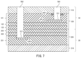
- FIG. 7 shows a state after performing step B 4 .
- step B 4 dry etching of the first opening 501 and the second opening 502 is advanced until the first electrode 301 and the second electrode 302 are reached. This dry etching step will be described in detail below.
- the dry etching apparatus to be used is desirably an etching apparatus capable of performing a Bosch process in order to collectively perform simultaneous etching of openings.
- An ICP etching apparatus can be exemplified as such a dry etching apparatus.
- the first wiring structure unit 120 and the second wiring structure unit 220 are assumed to be made of silicon oxide, silicon nitride, or silicon carbide. These multilayer films are desirably collectively etched and a fluorocarbon-based gas such as CF 4 is conceivable as an etching gas therefor. In this etching step, an additive gas such as O 2 , N a , He, or Ar may be used when appropriate.
- Wiring structure units 120 , 220 SiO+C x F y ⁇ SiF ⁇ +CO ⁇
- Wiring structure units 120 , 220 SiN+C x F y ⁇ +CN ⁇
- step B 2 Since an adjustment has been made in step B 2 so as to equalize a film thickness of insulating layers that remain on the respective electrodes 301 and 302 , etching reaches the first electrode 301 and the second electrode 302 at almost the same time. Accordingly, damage to the electrodes can be minimized.
- a portion of the first electrode 301 having been exposed by the first opening 501 becomes the first pad 311 for wire bonding.
- a portion of the second electrode 302 having been exposed by the second opening 502 becomes the second pad 312 for wire bonding.
- FIG. 8 shows a state after performing step C.
- the first wire 601 is bonded onto the first pad 311 being exposed at the bottom of the first opening 501 and, at the same time, the second wire 602 is bonded onto the second pad 312 being exposed at the bottom of the second opening 502 .
- the first wire 601 and the second wire 602 are, for example, wires made of gold or a gold alloy.
- a power supply structure to the first electrode 301 and the second electrode 302 that exist at different depths is realized by wire bonding, manufacturing cost can be reduced as compared to a structure that utilizes TSV.
- two openings with different depths are formed by simultaneous etching of openings (in other words, etching using a same photoresist), a manufacturing process can be simplified and, at the same time, openings for wire bonding with high reliability can be formed.
- an annular member made of a non-insulating material that is a residue of the etching stopper film 401 constitutes a part of an inner wall (a side surface) of the first opening 501 . Due to a gettering effect of the annular member, a secondary effect of reducing metal contamination from the first opening 501 can also be produced. It should be noted that a member made of the same material as the etching stopper film 401 does not exist on an inner wall (a side surface) of the second opening 502 . This is because, in step B 2 described earlier, a member that may become an etching stopper is not provided in a region where the second opening 502 is to be formed in order to ensure that only the etching of the second opening 502 is advanced.
- FIG. 9 A is a diagram showing a configuration of a stacked photoelectric conversion apparatus.
- a photoelectric conversion apparatus 1010 is constructed by laminating and electrically connecting two chips, namely, a sensor chip 11 and a circuit chip 21 .
- the sensor chip 11 corresponds to the first chip 10 in FIG. 1
- the circuit chip 21 corresponds to the second chip 20 in FIG. 1 .
- a pixel region 12 is arranged on the sensor chip 11 and a circuit region 22 for processing a signal detected by the pixel region 12 is arranged on the circuit chip 21 .
- FIG. 9 B is an arrangement diagram of the sensor chip 11 .
- Pixels 100 having a photoelectric conversion unit 101 that converts light into an electric signal are arranged in a two-dimensional pattern to form the pixel region 12 . While the pixel 100 is typically a pixel for forming an image, when used for time of flight (TOF), an image need not necessarily be formed. In other words, the pixel 100 may be a pixel for measuring a time point of arrival of light and a light amount.
- TOF time of flight
- FIG. 9 C is a configuration diagram of the circuit chip 21 .
- the circuit chip 21 has a signal processing unit 102 that processes a charge having been photoelectrically converted by the photoelectric conversion unit 101 in FIG. 9 B , a control pulse generating unit 109 , a horizontal scan circuit unit 104 , a signal line 107 , and a vertical scan circuit unit 103 .
- the photoelectric conversion unit 101 shown in FIG. 9 B and the signal processing unit 102 shown in FIG. 9 C are electrically connected via a connecting wiring provided for each pixel.
- the vertical scan circuit unit 103 receives a control pulse supplied from the control pulse generating unit 109 and supplies the control pulse to each pixel.
- a logic circuit such as a shift register or an address decoder is used in the vertical scan circuit unit 103 .
- a signal output from the photoelectric conversion unit 101 of each pixel is processed by the signal processing unit 102 .
- the signal processing unit 102 is provided with a counter and a memory and a digital signal is held in the memory.
- the horizontal scan circuit unit 104 inputs a control pulse for sequentially selecting each row to the signal processing unit 102 in order to read a signal from the memory of each pixel that holds a digital signal.
- a signal is output to the signal line 107 and a signal line 105 from the signal processing unit 102 of the pixel having been selected by the vertical scan circuit unit 103 .
- the signal output to the signal line 105 is output to an external recording unit or a signal processing unit of the photoelectric conversion apparatus 1010 via an output circuit 108 .
- the pixels 100 in the pixel region 12 may be arranged one-dimensionally.
- the circuit region 22 may be divided into a plurality of regions and the vertical scan circuit unit 103 and the horizontal scan circuit unit 104 may be arranged in each region.
- a function of the signal processing unit 102 need not necessarily be provided in each and every pixel 100 and, for example, a single signal processing unit 102 may be shared by a plurality of pixels 100 and signal processing may be performed sequentially.
- FIG. 10 is an example of a block diagram including the equivalent circuit shown in FIGS. 9 B and 9 C .
- the photoelectric conversion unit 101 having a photodiode 201 is provided in the sensor chip 11 and other members are provided in the circuit chip 21 .
- the photodiode 201 generates a charge pair in accordance with incident light by photoelectric conversion.
- a voltage VL first voltage
- a voltage VH second voltage
- the voltage VH is also supplied to circuits provided on the circuit chip 21 .
- the anode and the cathode of the photodiode 201 are supplied with voltages with a reverse bias that causes the photodiode 201 to act as an avalanche diode.
- the avalanche diode By creating a state where such voltages are supplied, a charge created by the incident light causes avalanche multiplication and an avalanche current is created.
- voltages of a reverse bias are supplied and a potential difference between the anode and the cathode is greater than a breakdown voltage, the avalanche diode enters a Geiger mode operation.
- the voltage VL (first voltage) is ⁇ 30 V and the voltage VH (second voltage) is 1.1 V.
- a quenching element 202 is connected to a power supply that supplies the voltage VH and to the photodiode 201 .
- the quenching element 202 has a function of replacing a change in the avalanche current created in the photodiode 201 with a voltage signal.
- the quenching element 202 functions as a load circuit (quenching circuit) during signal multiplication due to the avalanche multiplication and is responsible for suppressing the voltages to be supplied to the photodiode 201 to suppress avalanche multiplication (a quenching operation).
- the photodiode 201 provided in the sensor chip 11 and the quenching element 202 provided in the circuit chip 21 are electrically connected via a connecting wiring provided for each pixel.
- the signal processing unit 102 has a waveform shaping unit 203 , a counter circuit 209 , and a selection circuit 206 .
- the signal processing unit 102 need only have any of the waveform shaping unit 203 , the counter circuit 209 , and the selection circuit 206 .
- the counter circuit 209 is also the signal processing unit 102 .
- the waveform shaping unit 203 shapes a potential change of the cathode of the photodiode 201 that is obtained upon photon detection and outputs a pulse signal.
- an inverter circuit is used as the waveform shaping unit 203 . While an example in which a single inverter is used as the waveform shaping unit 203 is shown in FIG. 10 , a circuit in which a plurality of inverters are connected in series may be used or another circuit with a waveform shaping effect may be used.
- the counter circuit 209 counts pulse signals output from the waveform shaping unit 203 .
- the counter circuit 209 can count pulse signals due to a signal photon up to approximately 2 to the N-th power. The counted signals are held as detected signals.
- a control pulse pRES is supplied via a drive line 207 , the signals held in the counter circuit 209 are reset.
- the selection circuit 206 is supplied a control pulse pSEL via a drive line 208 shown in FIG. 10 (not illustrated in FIG. 9 C ) from the vertical scan circuit unit 103 shown in FIG. 9 C and switches between electric connection and non-connection of the counter circuit 209 and the signal line 107 .
- the selection circuit 206 includes a buffer circuit for outputting signals and the like.
- a switch such as a transistor may be arranged between the quenching element 202 and the photodiode 201 , the photoelectric conversion unit 101 and the signal processing unit 102 , and the like to switch between electric connection and non-connection.
- supply of the voltage VH or the voltage VL to be supplied to the photoelectric conversion unit 101 may be electrically switched using a switch such as a transistor.
- a captured image may be acquired by a rolling shutter operation in which a count of the counter circuit 209 is sequentially reset for each row and signals held in the counter circuit 209 are sequentially output for each row.
- a captured image may be acquired by a global electronic shutter operation in which a count of the counter circuit 209 of all pixel rows is simultaneously reset and signals held in the counter circuit 209 are sequentially output for each row.
- means for switching between performing and not performing a count of the counter circuit 209 is preferably provided.
- An example of the switching means is the switch described above.
- a configuration using the counter circuit 209 has been described in the present embodiment.
- a photoelectric conversion apparatus 1010 which acquires a pulse detection timing using a time to digital converter (hereinafter, TDC) and a memory in place of the counter circuit 209 may be adopted.
- TDC time to digital converter
- a generation timing of a pulse signal output from the waveform shaping unit 203 is converted into a digital signal by the TDC.
- the TDC is supplied with a control pulse pREF (a referential signal) via a drive line from the vertical scan circuit unit 103 shown in FIG. 9 C .
- the control pulse pREF as a reference, the TDC acquires, as a digital signal, a signal when an input timing of a signal output from each pixel via the waveform shaping unit 203 is considered relative time.
- a device including the semiconductor apparatus according to the first and second embodiments and a peripheral apparatus that is connected to the semiconductor apparatus will be described.
- a device to which the semiconductor apparatus according to the first and second embodiments can be applied may be an electronic device such as a camera or an information terminal, an office device such as a copier or a scanner, or a medical device such as an endoscope or a CT.
- a device to which the semiconductor apparatus according to the first and second embodiments can be applied may be an industrial device such as a robot or a semiconductor manufacturing apparatus, an analyzing device such as an electron microscope, or a transport device such as a vehicle, a vessel, or an airplane.
- FIG. 11 is a region diagram showing a configuration of the photoelectric conversion system 1200 according to the present embodiment.
- the photoelectric conversion system 1200 according to the present embodiment includes a photoelectric conversion apparatus 1204 . Any of the photoelectric conversion apparatuses described in the embodiments presented above can be applied to the photoelectric conversion apparatus 1204 .
- the photoelectric conversion system 1200 can be used as an imaging system. Specific examples of the imaging system include a digital still camera, a digital camcorder, and a monitoring camera. In FIG. 11 , a digital still camera is shown as an example of the photoelectric conversion system 1200 .
- the photoelectric conversion system 1200 shown in FIG. 11 has the photoelectric conversion apparatus 1204 , a lens 1202 that causes an optical image of a subject to be formed on the photoelectric conversion apparatus 1204 , an aperture 1203 for variably adjusting a passing light amount of the lens 1202 , and a barrier 1201 for protecting the lens 1202 .
- the lens 1202 and the aperture 1203 are optical systems for collecting light to the photoelectric conversion apparatus 1204 .
- the photoelectric conversion system 1200 has a signal processing unit 1205 for processing an output signal that is output from the photoelectric conversion apparatus 1204 .
- the signal processing unit 1205 performs operations of signal processing in which an input signal is subjected to various corrections and compression when necessary and the input signal is output.
- the photoelectric conversion system 1200 further has a buffer memory 1206 for temporarily storing image data and an external interface unit (an external I/F unit) 1209 for communicating with an external computer or the like.
- the photoelectric conversion system 1200 has a recording medium 1211 such as a semiconductor memory for recording or reading imaging data and a recording medium control interface unit (a recording medium control I/F unit) 1210 for performing recording and reading with respect to the recording medium 1211 .
- the recording medium 1211 may be built into the photoelectric conversion system 1200 or may be attachable to and detachable from the photoelectric conversion system 1200 .
- communication from the recording medium control I/F unit 1210 to the recording medium 1211 and communication from the external I/F unit 1209 may be performed in a wireless manner.
- the photoelectric conversion system 1200 has an overall control operating unit 1208 that performs various arithmetic operations and controls the entire digital still camera and a timing generating unit 1207 that outputs various timing signals to the photoelectric conversion apparatus 1204 and the signal processing unit 1205 .
- the timing signals and the like may be input from outside and the photoelectric conversion system 1200 need at least have the photoelectric conversion apparatus 1204 and the signal processing unit 1205 that processes an output signal that is output from the photoelectric conversion apparatus 1204 .
- the overall control operating unit 1208 and the timing generating unit 1207 may be configured so as to implement a part of or all of control functions of the photoelectric conversion apparatus 1204 .
- the photoelectric conversion apparatus 1204 outputs an image signal to the signal processing unit 1205 .
- the signal processing unit 1205 performs predetermined signal processing on the image signal output from the photoelectric conversion apparatus 1204 and outputs image data.
- the signal processing unit 1205 generates an image using the image signal.
- the signal processing unit 1205 may perform a ranging operation with respect to a signal output from the photoelectric conversion apparatus 1204 .
- the signal processing unit 1205 and the timing generating unit 1207 may be mounted to the photoelectric conversion apparatus. In other words, the signal processing unit 1205 and the timing generating unit 1207 may be provided in a chip in which pixels are arranged.
- FIG. 12 A is a schematic view of a photoelectric conversion system to the present embodiment
- FIGS. 12 B to 12 D are schematic views of a moving body according to the present embodiment
- FIG. 13 is a flow chart showing operations of the photoelectric conversion system according to the present embodiment.
- an example of a vehicle-mounted camera will be described as the photoelectric conversion system.
- FIG. 12 A shows an example of a vehicle system and a photoelectric conversion system which is mounted to the vehicle system and which performs imaging.
- the photoelectric conversion system 1301 includes a photoelectric conversion apparatus 1302 , an image preprocessing unit 1315 , an integrated circuit 1303 , and an optical system 1314 .
- the optical system 1314 forms an optical image of a subject on the photoelectric conversion apparatus 1302 .
- the photoelectric conversion apparatus 1302 converts the optical image of the subject having been formed by the optical system 1314 into an electric signal.
- the photoelectric conversion apparatus 1302 is the photoelectric conversion apparatus of any of the embodiments described above.
- the image preprocessing unit 1315 performs predetermined signal processing on a signal output from the photoelectric conversion apparatus 1302 .
- a function of the image preprocessing unit 1315 may be incorporated into the photoelectric conversion apparatus 1302 .
- the photoelectric conversion system 1301 is provided with at least two sets of the optical system 1314 , the photoelectric conversion apparatus 1302 , and the image preprocessing unit 1315 , and an output from the image preprocessing unit 1315 of each set is to be input to the integrated circuit 1303 .
- the integrated circuit 1303 is an integrated circuit intended for imaging system applications and includes an image processing unit 1304 including a memory 1305 , an optical ranging unit 1306 , a ranging operating unit 1307 , an object recognizing unit 1308 , and an abnormality detecting unit 1309 .
- the image processing unit 1304 performs image processing such as development processing and defect correction with respect to an output signal of the image preprocessing unit 1315 .
- the memory 1305 performs primary storage of captured images and stores detect positions of imaging pixels.
- the optical ranging unit 1306 performs focusing and ranging of a subject.
- the ranging operating unit 1307 calculates ranging information from a plurality of pieces of image data acquired by a plurality of photoelectric conversion apparatuses 1302 .
- the object recognizing unit 1308 recognizes a subject such as a vehicle, a road, a sign, or a person. Upon detecting an abnormality of the photoelectric conversion apparatus 1302 , the abnormality detecting unit 1309 issues an alarm about the abnormality to a main control unit 1313 .
- the integrated circuit 1303 may be realized by exclusively-designed hardware, a software module, or a combination thereof.
- the integrated circuit 1303 may be realized by a field programmable gate array (FPGA), an application specific integrated circuit (ASIC), or the like, or a combination thereof.
- FPGA field programmable gate array
- ASIC application specific integrated circuit
- the main control unit 1313 integrally controls operations of the photoelectric conversion system 1301 , a vehicle sensor 1310 , a control unit 1320 , and the like.
- a method may be adopted in which the main control unit 1313 is omitted and the photoelectric conversion system 1301 , the vehicle sensor 1310 , and the control unit 1320 individually have a communication interface and respectively transmit and receive control signals via a communication network (for example, the CAN standard).
- the integrated circuit 1303 has a function of transmitting control signals and setting values to the photoelectric conversion apparatus 1302 either in response to receiving a control signal from the main control unit 1313 or using its own control unit.
- the photoelectric conversion system 1301 is connected to the vehicle sensor 1310 and is capable of detecting a travel condition of a host vehicle such as a vehicle speed, a yaw rate, and a steering angle, an external environment of the host vehicle, and conditions of other vehicles and obstacles.
- the vehicle sensor 1310 is also distance information acquiring means which acquires information related to a distance to an object.
- the photoelectric conversion system 1301 is connected to a drive assist control unit 1311 that provides various drive assistance functions such as automatic steering, automatic cruising, and collision avoidance.
- a collision determination function estimation of a collision and determination of presence or absence of a collision with another vehicle or an obstacle are performed based on a detection result of the photoelectric conversion system 1301 or the vehicle sensor 1310 . Accordingly, avoidance control when a collision is estimated and activation of a safety device upon a collision are performed.
- the photoelectric conversion system 1301 is also connected to an alarm 1312 which issues a warning to a driver based on a determination result of a collision determining unit.
- the main control unit 1313 performs vehicle control involving applying the brakes, releasing the gas pedal, suppressing engine output, or the like to avoid a collision and/or reduce damage.
- the alarm 1312 issues a warning to a user by sounding an alarm or the like, displaying warning information on a screen of a display unit of a car navigation system, a meter panel, or the like, vibrating a seat belt or a steering wheel, or the like.
- FIGS. 12 B to 12 D show an example of an arrangement of the photoelectric conversion system 1301 when the front of the vehicle is imaged by the photoelectric conversion system 1301 .
- Two photoelectric conversion apparatuses 1302 are arranged in the front of a vehicle 1300 .
- a center line with respect to an advancing/retreating direction or an external shape (for example, a vehicle width) of the vehicle 1300 is likened to a symmetrical axis
- arranging the two photoelectric conversion apparatuses 1302 so as to be symmetrical about the symmetrical axis is preferable in terms of acquiring information on a distance between the vehicle 1300 and a photographed object and determining collision possibility.
- the photoelectric conversion apparatuses 1302 are preferably arranged so as not to impede a field of view of a driver when the driver views a state of the outside of the vehicle 1300 from the driver's seat.
- the alarm 1312 is preferably arranged so as to readily enter the driver's field of view.
- the failure detection operation by the photoelectric conversion apparatus 1302 in the photoelectric conversion system 1301 will be described with reference to FIG. 13 .
- the failure detection operation by the photoelectric conversion apparatus 1302 is carried out in accordance with steps S 1410 to S 1480 shown in FIG. 13 .
- Step S 1410 is a step of configuring settings upon start-up of the photoelectric conversion apparatus 1302 .
- settings for operating the photoelectric conversion apparatus 1302 are transmitted from outside of the photoelectric conversion system 1301 (for example, the main control unit 1313 ) or inside the photoelectric conversion system 1301 to start an imaging operation and the failure detection operation by the photoelectric conversion apparatus 1302 .
- step S 1420 a pixel signal is acquired from a valid pixel.
- step S 1430 an output value from a failure detection pixel having been provided for failure detection is acquired.
- the failure detection pixel includes a photoelectric conversion unit in a similar manner to the valid pixel. A predetermined voltage is written into the photoelectric conversion unit. The failure detection pixel outputs a signal corresponding to the voltage having been written into the photoelectric conversion unit. It should be noted that an order of steps S 1420 and S 1430 may be reversed.
- step S 1440 an applicability determination between an output expectation value of the failure detection pixel and an actual output value from the failure detection pixel is performed.
- step S 1440 when the output expectation value and the actual output value match, a transition is made to step S 1450 to determine that an imaging operation is being performed normally and processing advances to step S 1460 .
- step S 1460 a pixel signal of a scanned row is transmitted to and temporarily saved in the memory 1305 . Subsequently, a return is made to step S 1420 to continue the failure detection operation.
- step S 1440 when the output expectation value and the actual output value do not match, the processing makes a transition to step S 1470 .
- step S 1470 a determination that there is an abnormality in the imaging operation is made and a warning is issued to the main control unit 1313 or the alarm 1312 .
- the alarm 1312 causes the display unit to display the fact that an abnormality has been detected.
- step S 1480 the photoelectric conversion apparatus 1302 is stopped and operations of the photoelectric conversion system 1301 are ended.
- the flow chart may be looped every plurality of rows or the failure detection operation may be performed for each frame.
- the warning issued in step S 1470 may be notified to the outside the vehicle via a wireless network.
- the photoelectric conversion system 1301 can also be applied to controlling automated driving so that the vehicle follows another vehicle, controlling automated driving so that the vehicle stays within a lane, and the like.
- the photoelectric conversion system 1301 is not limited to a vehicle such as an automobile and can also be applied to a moving body (a moving apparatus) such as a ship, an airplane, or an industrial robot.
- the photoelectric conversion apparatus can be applied to a wide variety of devices that utilize object recognition such as an intelligent transportation system (ITS).
- ITS intelligent transportation system
- an electric path in a semiconductor apparatus can be improved.
Landscapes
- Internal Circuitry In Semiconductor Integrated Circuit Devices (AREA)
- Solid State Image Pick-Up Elements (AREA)
- Transforming Light Signals Into Electric Signals (AREA)
Applications Claiming Priority (2)
| Application Number | Priority Date | Filing Date | Title |
|---|---|---|---|
| JP2020-060351 | 2020-03-30 | ||
| JP2020060351A JP2021158320A (ja) | 2020-03-30 | 2020-03-30 | 半導体装置及びその製造方法、機器 |
Publications (2)
| Publication Number | Publication Date |
|---|---|
| US20210305439A1 US20210305439A1 (en) | 2021-09-30 |
| US11728441B2 true US11728441B2 (en) | 2023-08-15 |
Family
ID=77856478
Family Applications (1)
| Application Number | Title | Priority Date | Filing Date |
|---|---|---|---|
| US17/214,637 Active 2041-10-12 US11728441B2 (en) | 2020-03-30 | 2021-03-26 | Semiconductor apparatus and manufacturing method thereof, and device |
Country Status (2)
| Country | Link |
|---|---|
| US (1) | US11728441B2 (enExample) |
| JP (1) | JP2021158320A (enExample) |
Families Citing this family (2)
| Publication number | Priority date | Publication date | Assignee | Title |
|---|---|---|---|---|
| JP2023099398A (ja) * | 2022-01-01 | 2023-07-13 | キヤノン株式会社 | 光電変換装置、撮像システム、光検出システム、および移動体 |
| US20250142983A1 (en) * | 2023-10-30 | 2025-05-01 | Globalfoundries Singapore Pte. Ltd. | Single-photon avalanche diodes with hybrid trench isolation structures |
Citations (13)
| Publication number | Priority date | Publication date | Assignee | Title |
|---|---|---|---|---|
| US20080246152A1 (en) * | 2007-04-04 | 2008-10-09 | Taiwan Semiconductor Manufacturing Co., Ltd. | Semiconductor device with bonding pad |
| US20130222657A1 (en) | 2012-02-29 | 2013-08-29 | Canon Kabushiki Kaisha | Solid-state image sensor and method of manufacturing the same |
| US20130299886A1 (en) * | 2012-05-10 | 2013-11-14 | Taiwan Semiconductor Manufacturing Company, Ltd. | Backside Structure and Methods for BSI Image Sensors |
| US20140091414A1 (en) | 2012-09-28 | 2014-04-03 | Canon Kabushiki Kaisha | Semiconductor apparatus |
| JP2014072295A (ja) | 2012-09-28 | 2014-04-21 | Canon Inc | 半導体装置の製造方法 |
| US20140124889A1 (en) * | 2012-11-05 | 2014-05-08 | Omnivision Technologies, Inc. | Die seal ring for integrated circuit system with stacked device wafers |
| US20160233264A1 (en) * | 2013-10-04 | 2016-08-11 | Sony Corporation | Semiconductor device and solid-state imaging device |
| US20170221950A1 (en) * | 2016-01-29 | 2017-08-03 | Taiwan Semiconductor Manufacturing Co., Ltd. | Metal Block and Bond Pad Structure |
| US9887229B2 (en) * | 2015-08-04 | 2018-02-06 | Xintec Inc. | Sensing chip package and a manufacturing method thereof |
| US20180374795A1 (en) * | 2016-02-23 | 2018-12-27 | Renesas Electronics Corporation | Semiconductor device and method of manufacturing the same |
| WO2019010320A1 (en) * | 2017-07-05 | 2019-01-10 | Ouster, Inc. | ELECTRONIC SCANNING EMITTER NETWORK LIGHT EMITTING DEVICE AND SYNCHRONIZED SENSOR ARRAY |
| DE102019124181A1 (de) * | 2018-09-28 | 2020-04-02 | Taiwan Semiconductor Manufacturing Co., Ltd. | Vereinzelungsverfahren für gestapelte halbleiterbauelemente |
| US20200105814A1 (en) * | 2017-04-04 | 2020-04-02 | Sony Semiconductor Solutions Corporation | Solid-state imaging device and electronic apparatus |
Family Cites Families (8)
| Publication number | Priority date | Publication date | Assignee | Title |
|---|---|---|---|---|
| JPH09116014A (ja) * | 1995-10-20 | 1997-05-02 | Nippon Steel Corp | 半導体装置の製造方法 |
| US8502335B2 (en) * | 2009-07-29 | 2013-08-06 | Taiwan Semiconductor Manufacturing Company, Ltd. | CMOS image sensor big via bonding pad application for AlCu Process |
| JP2014183116A (ja) * | 2013-03-18 | 2014-09-29 | Asahi Kasei Electronics Co Ltd | 半導体装置の製造方法及び半導体装置 |
| JP6308727B2 (ja) * | 2013-06-13 | 2018-04-11 | キヤノン株式会社 | 電子デバイスの製造方法 |
| JP5950888B2 (ja) * | 2013-11-19 | 2016-07-13 | 冨士薬品工業株式会社 | 固体撮像素子の製造方法 |
| JP7178605B2 (ja) * | 2017-03-22 | 2022-11-28 | パナソニックIpマネジメント株式会社 | 固体撮像装置 |
| US11411037B2 (en) * | 2017-04-04 | 2022-08-09 | Sony Semiconductor Solutions Corporation | Solid-state imaging device and electronic apparatus including coupling structures for electrically interconnecting stacked semiconductor substrates |
| JP7039310B2 (ja) * | 2018-02-09 | 2022-03-22 | キヤノン株式会社 | 光電変換装置及び撮像システム |
-
2020
- 2020-03-30 JP JP2020060351A patent/JP2021158320A/ja active Pending
-
2021
- 2021-03-26 US US17/214,637 patent/US11728441B2/en active Active
Patent Citations (13)
| Publication number | Priority date | Publication date | Assignee | Title |
|---|---|---|---|---|
| US20080246152A1 (en) * | 2007-04-04 | 2008-10-09 | Taiwan Semiconductor Manufacturing Co., Ltd. | Semiconductor device with bonding pad |
| US20130222657A1 (en) | 2012-02-29 | 2013-08-29 | Canon Kabushiki Kaisha | Solid-state image sensor and method of manufacturing the same |
| US20130299886A1 (en) * | 2012-05-10 | 2013-11-14 | Taiwan Semiconductor Manufacturing Company, Ltd. | Backside Structure and Methods for BSI Image Sensors |
| US20140091414A1 (en) | 2012-09-28 | 2014-04-03 | Canon Kabushiki Kaisha | Semiconductor apparatus |
| JP2014072295A (ja) | 2012-09-28 | 2014-04-21 | Canon Inc | 半導体装置の製造方法 |
| US20140124889A1 (en) * | 2012-11-05 | 2014-05-08 | Omnivision Technologies, Inc. | Die seal ring for integrated circuit system with stacked device wafers |
| US20160233264A1 (en) * | 2013-10-04 | 2016-08-11 | Sony Corporation | Semiconductor device and solid-state imaging device |
| US9887229B2 (en) * | 2015-08-04 | 2018-02-06 | Xintec Inc. | Sensing chip package and a manufacturing method thereof |
| US20170221950A1 (en) * | 2016-01-29 | 2017-08-03 | Taiwan Semiconductor Manufacturing Co., Ltd. | Metal Block and Bond Pad Structure |
| US20180374795A1 (en) * | 2016-02-23 | 2018-12-27 | Renesas Electronics Corporation | Semiconductor device and method of manufacturing the same |
| US20200105814A1 (en) * | 2017-04-04 | 2020-04-02 | Sony Semiconductor Solutions Corporation | Solid-state imaging device and electronic apparatus |
| WO2019010320A1 (en) * | 2017-07-05 | 2019-01-10 | Ouster, Inc. | ELECTRONIC SCANNING EMITTER NETWORK LIGHT EMITTING DEVICE AND SYNCHRONIZED SENSOR ARRAY |
| DE102019124181A1 (de) * | 2018-09-28 | 2020-04-02 | Taiwan Semiconductor Manufacturing Co., Ltd. | Vereinzelungsverfahren für gestapelte halbleiterbauelemente |
Also Published As
| Publication number | Publication date |
|---|---|
| JP2021158320A (ja) | 2021-10-07 |
| US20210305439A1 (en) | 2021-09-30 |
Similar Documents
| Publication | Publication Date | Title |
|---|---|---|
| US12021108B2 (en) | Photoelectric conversion apparatus, photoelectric conversion system, and moving object | |
| CN110138364B (zh) | 光电转换装置及摄像系统 | |
| US11411028B2 (en) | Photoelectric conversion apparatus, photoelectric conversion system, and moving object | |
| TWI782208B (zh) | 成像設備、成像系統、移動體以及用於層壓的半導體基板 | |
| US11601608B2 (en) | Photoelectric conversion apparatus, photoelectric conversion system, and moving body | |
| US10504954B2 (en) | Imaging device, imaging system, and moving body | |
| US11798970B2 (en) | Semiconductor apparatus and equipment | |
| US20250201639A1 (en) | Semiconductor device, manufacturing method thereof, and electronic apparatus | |
| US11728441B2 (en) | Semiconductor apparatus and manufacturing method thereof, and device | |
| EP4075793A1 (en) | Imaging device and electronic apparatus | |
| JP2021125491A (ja) | 半導体装置、半導体システム、移動体 | |
| US20240395844A1 (en) | Photoelectric conversion device, method for producing the same, and appliance | |
| JP2022087547A (ja) | 光電変換装置、光電変換システム、および移動体 | |
| JP2025058593A (ja) | 光電変換装置、機器、および移動体 | |
| JP7558822B2 (ja) | 光電変換装置、光電変換システム、および移動体 | |
| US12501187B2 (en) | Photoelectric conversion apparatus, device, and moving body | |
| US20240405051A1 (en) | Photoelectric conversion apparatus, photoelectric conversion system, and moving body | |
| US20250006769A1 (en) | Photoelectric conversion device, photoelectric conversion system, and moving body | |
| US20240304648A1 (en) | Solid-state imaging device and manufacturing method for solid-state imaging device | |
| US20250311474A1 (en) | Semiconductor apparatus, photoelectric conversion system and moving body | |
| US20240357263A1 (en) | Photoelectric conversion device, photoelectric conversion system, moving body, and semiconductor substrate | |
| JP2021019058A (ja) | 光電変換装置および機器 | |
| CN116802810A (zh) | 光电转换装置、光电转换系统及移动体 |
Legal Events
| Date | Code | Title | Description |
|---|---|---|---|
| FEPP | Fee payment procedure |
Free format text: ENTITY STATUS SET TO UNDISCOUNTED (ORIGINAL EVENT CODE: BIG.); ENTITY STATUS OF PATENT OWNER: LARGE ENTITY |
|
| AS | Assignment |
Owner name: CANON KABUSHIKI KAISHA, JAPAN Free format text: ASSIGNMENT OF ASSIGNORS INTEREST;ASSIGNORS:HAYASHI, HIDEKI;IWATA, JUNJI;TORII, KEITA;AND OTHERS;SIGNING DATES FROM 20210311 TO 20210315;REEL/FRAME:056177/0263 |
|
| STPP | Information on status: patent application and granting procedure in general |
Free format text: DOCKETED NEW CASE - READY FOR EXAMINATION |
|
| STPP | Information on status: patent application and granting procedure in general |
Free format text: NON FINAL ACTION MAILED |
|
| STPP | Information on status: patent application and granting procedure in general |
Free format text: PUBLICATIONS -- ISSUE FEE PAYMENT VERIFIED |
|
| STCF | Information on status: patent grant |
Free format text: PATENTED CASE |