US11611642B2 - Mobile terminal, housing, and method for manufacturing housing - Google Patents
Mobile terminal, housing, and method for manufacturing housing Download PDFInfo
- Publication number
- US11611642B2 US11611642B2 US17/508,922 US202117508922A US11611642B2 US 11611642 B2 US11611642 B2 US 11611642B2 US 202117508922 A US202117508922 A US 202117508922A US 11611642 B2 US11611642 B2 US 11611642B2
- Authority
- US
- United States
- Prior art keywords
- light
- main body
- transparent
- shielding layer
- hole
- Prior art date
- Legal status (The legal status is an assumption and is not a legal conclusion. Google has not performed a legal analysis and makes no representation as to the accuracy of the status listed.)
- Active, expires
Links
Images


Classifications
-
- H—ELECTRICITY
- H04—ELECTRIC COMMUNICATION TECHNIQUE
- H04M—TELEPHONIC COMMUNICATION
- H04M1/00—Substation equipment, e.g. for use by subscribers
- H04M1/02—Constructional features of telephone sets
- H04M1/0202—Portable telephone sets, e.g. cordless phones, mobile phones or bar type handsets
- H04M1/0249—Details of the mechanical connection between the housing parts or relating to the method of assembly
-
- H—ELECTRICITY
- H04—ELECTRIC COMMUNICATION TECHNIQUE
- H04M—TELEPHONIC COMMUNICATION
- H04M1/00—Substation equipment, e.g. for use by subscribers
- H04M1/02—Constructional features of telephone sets
- H04M1/0202—Portable telephone sets, e.g. cordless phones, mobile phones or bar type handsets
- H04M1/0279—Improving the user comfort or ergonomics
- H04M1/0283—Improving the user comfort or ergonomics for providing a decorative aspect, e.g. customization of casings, exchangeable faceplate
-
- H—ELECTRICITY
- H04—ELECTRIC COMMUNICATION TECHNIQUE
- H04M—TELEPHONIC COMMUNICATION
- H04M1/00—Substation equipment, e.g. for use by subscribers
- H04M1/02—Constructional features of telephone sets
- H04M1/0202—Portable telephone sets, e.g. cordless phones, mobile phones or bar type handsets
- H04M1/026—Details of the structure or mounting of specific components
- H04M1/0266—Details of the structure or mounting of specific components for a display module assembly
-
- H—ELECTRICITY
- H04—ELECTRIC COMMUNICATION TECHNIQUE
- H04M—TELEPHONIC COMMUNICATION
- H04M1/00—Substation equipment, e.g. for use by subscribers
- H04M1/02—Constructional features of telephone sets
- H04M1/0202—Portable telephone sets, e.g. cordless phones, mobile phones or bar type handsets
- H04M1/026—Details of the structure or mounting of specific components
- H04M1/0274—Details of the structure or mounting of specific components for an electrical connector module
-
- H—ELECTRICITY
- H04—ELECTRIC COMMUNICATION TECHNIQUE
- H04M—TELEPHONIC COMMUNICATION
- H04M1/00—Substation equipment, e.g. for use by subscribers
- H04M1/02—Constructional features of telephone sets
- H04M1/23—Construction or mounting of dials or of equivalent devices; Means for facilitating the use thereof
- H04M1/236—Construction or mounting of dials or of equivalent devices; Means for facilitating the use thereof including keys on side or rear faces
Definitions
- the present disclosure relates to the field of mobile terminals, and in particular to a mobile terminal, a housing, and a method for manufacturing the housing.
- the transparent housings are designed as transparent structures to show a good luster.
- the transparent housings have some problems. For example, on the transparent housing, holes corresponding to an earphone jack, a button or a charging interface are provided, a side wall of each of the hole passes through the transparent housing and thus a bright spot or light-spot is formed on the surface of the transparent housing, which affects the overall appearance and texture of the transparent housing and the respective mobile terminal.
- a housing for a mobile terminal in the embodiments of the present disclosure.
- the housing includes a transparent main body and a light-shielding layer.
- the transparent main body has an outer surface and an inner surface opposite to each other.
- the transparent main body includes a flat plate portion and a side portion connected with each other.
- the side portion is disposed at a periphery of the flat plate portion, and encloses the flat plate portion.
- the side portion is provided with a through hole penetrating both the inner surface and the outer surface.
- the light-shielding layer is provided at the outer surface of the transparent main body, and the light-shielding layer is located around the through hole.
- An end of side wall of the through hole that is away from the inner surface is connected to the light-shielding layer.
- An orthographic projection area of the side wall of the through hole on a reference plane is located within an orthographic projection area of the light-shielding layer on the reference plane, and the reference plane is a geometric plane in parallel with the flat plate portion.
- a method for manufacturing the housing in the embodiments of the present disclosure.
- the method includes: providing a transparent main body.
- the transparent main body has an outer surface and an inner surface opposite to each other.
- the transparent main body includes a flat plate portion and a side portion connected with each other, and the side portion is disposed at a periphery of the flat plate portion and encloses the flat plate portion.
- the method further includes: providing a light-shielding layer at the outer surface of the transparent main body; and providing a through hole in the side portion. The through hole penetrates both the inner surface and the outer surface.
- the light-shielding layer is located around the through hole, and an end of a side wall of the through hole that is away from the inner surface is connected to the light-shielding layer.
- An orthographic projection area of the light-shielding layer on a reference plane covers an orthographic projection area of the side wall of the through hole on the reference plane, and the reference plane is a geometric plane in parallel with the flat plate portion.
- a mobile terminal in the embodiments of the present disclosure.
- the mobile terminal includes a display screen and the housing mentioned above.
- the display screen is installed on the housing.
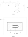
- FIG. 1 is a perspective view of a mobile terminal provided by the embodiments of the disclosure.
- FIG. 2 is a schematic diagram illustrating a structure of a housing of the mobile terminal according an embodiment of the disclosure, in which a virtual first reference plane and a virtual second reference plane are correspondingly shown.
- FIG. 3 is a schematic diagram illustrating a part of the structure of the housing shown in FIG. 2 .
- FIG. 4 is a schematic diagram illustrating a cross section taken along a middle line I-I shown in FIG. 3 , in which the virtual first reference surface and second reference surface are correspondingly shown.
- FIG. 5 is a schematic diagram illustrating orthographic projections of an inner wall of a through hole and a light-shielding layer on the second reference plane for the housing according to an embodiment of the disclosure.
- FIG. 6 is a schematic diagram illustrating orthographic projections of the inner wall of the through hole and the light-shielding layer on the second reference plane according to another embodiment of the disclosure.
- FIG. 7 is a schematic diagram illustrating a part of the structure of the housing according to another embodiment of the disclosure.
- FIG. 8 is a schematic diagram illustrating a cross section taken along a middle line II-II shown in FIG. 7 .
- FIG. 9 is a schematic diagram illustrating a cross section of the housing according to another embodiment of the disclosure.
- FIG. 10 is a flowchart of a method for manufacturing a housing according to an embodiment of the disclosure.
- FIG. 11 is a flowchart of a method for manufacturing a housing according to another embodiment of the disclosure.
- FIG. 12 is another schematic diagram illustrating the cross section taken along the middle line I-I shown in FIG. 3 , in which an ink layer between the light-shielding layer and the transparent main body is shown.
- terminal device refers to, but is not limited to, devices that can be connected in any one or some of the following connections to receive and/or send communication signals:
- Wired connection for example, the connection is established via Public Switched Telephone Networks (PSTN), Digital Subscriber Line (DSL), a digital cable, and a direct cable; and
- PSTN Public Switched Telephone Networks
- DSL Digital Subscriber Line
- Wireless connection for example, the connection is established via cellular network, Wireless Local Area Network (WLAN), digital television network such as DVB-H network, satellite network, and AM-FM broadcast transmitter.
- WLAN Wireless Local Area Network
- DVB-H network digital television network
- satellite network satellite network
- AM-FM broadcast transmitter AM-FM broadcast transmitter
- mobile terminals configured to communicate wirelessly
- mobile terminals include, but are not limited to, the following electronic devices:
- a satellite phone or cellular phone (1) A satellite phone or cellular phone;
- PCS Personal Communications System
- the mobile terminal 100 may be a smart phone, a computer, an IPAD or other electronic devices, which is not limited herein.
- the mobile terminal 100 provided by the embodiments is illustrated by taking a mobile phone as an example.
- the mobile terminal 100 includes a housing 10 and a display screen 20 .
- the display screen 20 can be installed on the housing 10 , and the housing can also be used to accommodate electronic components of the mobile terminal 100 , such as a battery and a mainboard.
- an edge of the display screen 20 is substantially joined with an edge of the housing 10 .
- the housing 10 includes a transparent main body 110 that is integrally formed.
- the transparent main body 110 has an outer surface 101 and an inner surface 102 opposite to each other.
- the inner surface 102 refers to a surface of the housing 10 which is invisible when the housing 10 is assembled on the mobile terminal 100 .
- the outer surface 101 is a surface of the housing 100 away from the interior of the mobile terminal 100 , which defines a part of the surface of the mobile terminal 100 .
- the transparent main body 110 may be made from transparent resin or plastic.
- the transparent main body 110 is made from a transparent polycarbonate material, transparent acrylic, or other transparent materials with excellent light transmission properties.
- the transparent main body 110 includes a flat plate portion 11 and a side portion 12 connected to each other.
- the side portion 12 is disposed at the periphery of the flat plate portion 11 and encloses the flat plate portion 11 .
- the side portion 12 is provided with at least one through hole 14 .
- Each of the through hole 14 may be a hole provided on the housing 10 for exposing the corresponding functional structure of the mobile terminal 100 .
- the location and the shape of each through hole 14 is set according to corresponding function structure of the mobile terminal 100 .
- the through hole 14 shown in FIG. 2 may be a USB interface hole for exposing a charging or data transmission interface of the mobile terminal 100 .
- the through hole 14 penetrates the inner surface 102 and the outer surface 101 .
- the through hole 14 may also be implemented as a hole for earphone jack 10 a of the mobile terminal 100 shown in FIG. 1 .
- the through hole 14 may also be implemented as a hole for button 10 b on the housing 10 that corresponds to a button 100 a of the mobile terminal 100 .
- the type of the through hole 14 is not limited herein.
- the structure of the housing 10 will be further described below by taking a case where the through hole 14 shown in FIG. 2 corresponds to the charging or data transmission interface of the mobile terminal 100 as an example.
- a light-shielding layer 13 is provided at the outer surface 101 of the transparent main body 110 .
- the light-shielding layer 13 is jointed with a side wall 141 of the through hole 14 .
- the light-shielding layer 13 extends along the outer surface 101 and is jointed with the side wall 141 of the through hole 14 . That is, the light-shielding layer 13 extends along the outer surface 101 and is located around the through hole 14 , and an end of the through hole 14 away from the inner surface 102 is connected to the light-shielding layer 13 .
- FIG. 1 In order to facilitate the definition of the arrangement of the light-shielding layer 13 and the side wall 141 of the through hole 14 , in FIG.
- a first virtual plane i.e., a first reference plane S 1
- the first reference plane S 1 is a geometric plane in parallel with the flat plate portion 11 .
- An orthographic projection area of the side wall 141 of the through hole 14 on the first reference plane S 1 is located within an orthographic projection area of the light-shielding layer 13 on the first reference plane S 1 .
- the orthographic projection area of the light-shielding layer 13 on the first reference plane S 1 can cover and shield the orthographic projection area of the side wall 141 of the through hole 14 on the first reference plane S 1 .
- a geometric plane perpendicular to a thickness direction of the mobile terminal 100 may also be defined as the first reference plane, and the arrangement of the light-shielding layer 13 also satisfies a condition that the orthographic projection area of the side wall 141 of the through hole 14 on the first reference plane S 1 is located within the orthographic projection area of the light-shielding layer 13 on the first reference plane S 1 .
- the light-shielding layer 13 provided at the outer surface 101 of the transparent main body 110 , the light is blocked.
- the orthographic projection area of the light-shielding layer 13 on the first reference plane S 1 covers the orthographic projection area of the side wall 141 of the through hole 14 on the first reference plane S 1 , in this way, the part of the transparent main body 110 that is provided with the light-shielding layer 13 has no optical transparency or has an extremely low light transmittance, and the side wall 141 of the through hole 14 cannot be observed through the part of the transparent main body 110 that is provided with the light-shielding layer 13 , thereby preventing the overall visual effect of the housing 10 from being affected by the visibility of the side wall 141 of the through hole 14 through the transparent main body 110 .
- the provided light-shielding layer 13 can shield the side wall 141 of the through hole 14 , and reduce the adverse effect on the outer surface 101 of the housing 10 that is caused by the visibility of the side wall 141 of the through hole 14 through the transparent main body 110 , thereby improving the overall appearance and texture of the housing 10 and the user experience.
- the part of the transparent main body 110 that is provided with the light-shielding layer 13 can be set according to requirements, as long as the side wall 141 of the through hole 14 can be shielded.
- the side wall 141 of the through hole 14 may be completely shielded by the light-shielding layer 13 . That is, the side wall 141 of the through hole 14 cannot be observed from the outer surface 101 of the housing 10 .
- the side wall 141 of the through hole 14 not being observed from the outer surface 101 of the housing 10 , it means that, when the observation point Y is on the side where the outer surface 101 of the housing 10 is located, neither the part of the transparent main body 110 that is provided with the light-shielding layer 13 nor a part of the transparent main body 110 that is not provided with the light-shielding layer 13 , enables the side wall 141 of the through hole 14 to be visible on the side where the outer surface 101 is located.
- the part of the transparent main body 110 that is not provided with the light-shielding layer 13 may have a reduced light transmittance due to the accumulation of materials of the transparent main body 110 along a propagation path of light; accordingly, this enables the side wall 141 of the through hole 14 to be invisible through the transparent main body 110 , or enables only a small amount of light reflected or diffusely reflected by the side wall 141 to pass through the transparent main body 110 , which is insufficient to be visually observed by naked eyes.
- all the light-shielding layer 13 is provided at the side portion 12 , thereby preventing the side wall 141 of the through hole 14 from being visible through a part of the outer surface 101 corresponding to the side wall 141 .
- one part of the light-shielding layer 13 is provided at the flat plate portion 11 , and the other part of the light-shielding layer 13 is provided at the side portion 12 , thereby further improving the shielding of the side wall 141 of the through hole 14 by the light-shielding layer 13 .
- some texture or color can also be formed on the light-shielding layer 13 , to achieve a good decorative effect and further improve the overall appearance and texture of the housing 10 .
- a second reference plane S 2 is defined by a geometric plane perpendicular to an extending direction of the through hole 14 .
- the extending direction of the through hole 14 refers to a depth direction of the through hole 14 provided in the housing 10 .
- the extending direction can also be considered to be along an axis direction of the through hole 14 .
- the through hole 14 penetrates the inner surface 102 and the outer surface 101 along the extending direction.
- an orthographic projection of the side wall 141 of the through hole 14 on the second reference plane S 2 defines a first contour line 14 a , and the shape of the area enclosed by the first contour line 14 a is the same as the shape of the cross section of the side wall 141 of the through hole 14 perpendicular to the extending direction.
- An orthographic projection of the light-shielding layer 13 on the second reference plane S 2 defines an enclosed area.
- the enclosed area has an inner edge 131 and an outer edge 132 .
- the inner edge 131 coincides with the first contour line 14 a , and the inner edge 131 is located in an area enclosed by the outer edge 132 .
- the area enclosed by the inner edge 131 is oblong, and the area enclosed by the outer edge 132 is rectangular. As shown in FIG. 6 , in other embodiments, the area enclosed by the inner edge 131 is elliptical, and the area enclosed by the outer edge 132 is rectangular.
- the through hole 14 serves as a hole in the housing 10 for exposing the functional structure of the mobile terminal 100 , and the shape of the through hole 14 can be set according to actual requirements. For example, when the through hole 14 is used as a hole for earphone jack, the area enclosed by the first contour line 14 a is circular, and the cross section of the through hole 14 is circular accordingly.
- the area enclosed by the outer edge 132 is rectangular, oblong or elliptical, such different shapes can adapt the overall appearance of the housing 10 .
- the shape of the area enclosed by the outer edge 132 is not limited herein.
- an angle ⁇ between the first reference plane S 1 and the second reference plane S 2 is in a range from 85° to 95°. Since the extending direction of the through hole 14 is perpendicular to the second reference plane S 2 , and the flat plate portion 11 is substantially perpendicular to the second reference plane S 2 , the angle ⁇ between the first reference plane S 1 and the second reference plane S 2 being in the range from 85° to 95° means that, an angle at which the extending direction of the through hole 14 is inclined relative to the flat plate portion 11 is within an range from ⁇ 5° to 5°, and the extending direction of the through hole 14 is substantially in parallel with the flat plate portion 11 .
- the angle ⁇ is 90°
- the extending direction of the through hole 14 is in parallel with the flat plate portion 11 .
- the flat plate portion 11 has a first surface 11 a and a second surface 11 b opposite to each other.
- the side portion 12 has an inner peripheral surface 12 a and an outer peripheral surface 12 b opposite to each other.
- the first surface 11 a and the inner peripheral surface 12 a form a part or all of the inner surface 102
- the outer peripheral surface 12 b is joined with the second surface 11 b to form the outer surface 101 .
- At least a part of the outer peripheral surface 12 b is an arc surface, the through hole 14 penetrates the arc surface.
- the arc surface enables the edge of the housing 100 to be smooth.
- a transparent hardened layer 15 is formed, by means of surface treatment, on the side where the outer surface is located.
- the transparent hardened layer 15 includes a first transparent hardened layer 151 and a second transparent hardened layer 152 , and the second transparent hardened layer 152 is jointed with the first transparent hardened layer 151 .
- the first transparent hardened layer 151 is disposed on the part of the outer surface 101 that is not provided with the light-shielding layer 13
- the second transparent hardened layer 152 is disposed on a side of the light-shielding layer 13 away from the transparent main body 110 .
- the surface strength of the housing 10 can be enhanced; in addition, the light-shielding layer 13 is sandwiched between the second transparent hardened layer 152 and the transparent main body 110 , which prevents the light-shielding layer 13 from falling off the transparent main body 110 , and thus prevents the overall appearance of the housing 10 from being influenced.
- the transparent hardened layer 15 may be made from tempered glass, ordinary glass, transparent plastic or transparent rubber.
- a decorative layer 16 is disposed on the inner surface 102 .
- the decorative layer 16 is made from an opaque material to prevent the internal structure of the mobile terminal 100 from being observed through the housing 10 , and thus prevents the overall appearance and texture of the mobile terminal 100 from being influenced.
- the display screen 20 may be a Liquid Crystal Display (LCD) screen for information display.
- the LCD screen may be a Thin Film Transistor (TFT) screen, or an In-Plane Switching (IPS) screen, or a Splice Liquid Crystal Display (SLCD) screen.
- TFT Thin Film Transistor
- IPS In-Plane Switching
- SLCD Splice Liquid Crystal Display
- the display screen 20 may be an Organic Light-Emitting Diode (OLED) screen for information display.
- OLED Organic Light-Emitting Diode
- the OLED screen may be an Active Matrix Organic Light Emitting Diode (AMOLED) screen, or a Super Active Matrix Organic Light Emitting Diode (Super AMOLED) screen, or a Super Active Matrix Organic Light Emitting Diode Plus (Super AMOLED Plus) screen, which is not limited herein.
- a method for manufacturing the housing 10 is provided in the embodiments of the present disclosure, which includes the following operations S 110 to S 130 :
- a transparent main body 110 is provided, where the transparent main body 110 includes a flat plate portion 11 and a side portion 12 connected with each other, and the side portion 12 is disposed at a periphery of the flat plate portion 11 and encloses the flat plate portion;
- a light-shielding layer 13 is formed at an outer surface 101 of the transparent main body 110 ;
- a through hole 14 is provided in the side portion 12 , where the through hole 14 penetrates an inner surface 102 and the outer surface 101 of the transparent main body 110 .
- the light-shielding layer 13 is jointed with a side wall 141 of the through hole 14 .
- An orthographic projection area of the light-shielding layer 13 on a first reference plane S 1 covers an orthographic projection area of the side wall 141 of the through hole 14 on the first reference plane S 1 , and the first reference plane S 1 is a geometric plane in parallel with the flat plate portion 11 .
- the side wall 141 of the through hole 14 can be shielded by means of the light-shielding layer 13 , and the overall appearance and texture of the housing 10 can thus be prevented from being influenced by the visibility of the side wall 141 of the through hole 14 through the transparent main body 110 .
- the operation of forming the light-shielding layer 13 at the outer surface 101 of the transparent main body 110 includes:
- the screen printing process that is, by applying ink onto a screen plate provided with characters or patterns in advance and applying a pressure thereto, the ink can be transferred, through screen printing, pad printing, transfer printing, or printing, to the outer surface 101 of the transparent main body 110 , so as to form the light-shielding layer 13 on the outer surface 101 of the transparent main body 110 .
- the thickness of the light-shielding layer 13 is in a range from 0.02 mm to 0.04 mm. Within such range, the light-shielding layer is not too thin to easily cause light leakage which would otherwise affect the shielding effect, and in another aspect, the light-shielding layer is not too thick to account for a large proportion of the total thickness of the housing 10 which would otherwise have an adverse effect on the overall structural strength of the housing 10 .
- the thickness of the light-shielding layer 13 is 0.02 mm. In other embodiments, the thickness of the light-shielding layer 13 may be 0.04 mm. In some embodiments, the thickness of the light-shielding layer 13 may be 0.03 mm. The thickness of the light-shielding layer 13 can be set according to the overall thickness of the housing 10 , which is not limited herein.
- the transparent main body 110 is integrally formed by an injection molding process with a transparent material.
- a cavity of a mold adopted for forming the transparent main body 110 has raised grains.
- the light-shielding layer 13 is formed by the transparent material filled into the recess formed between the raised grains.
- a depth of the recess formed between the raised grains is in a range from 0.01 mm to 0.05 mm, so that the light-shielding layer 13 , formed by the transparent material that is filled into the recess formed between the raised grains, has an appropriate thickness.
- the through hole 14 may be provided on the side portion 12 by removing a part of the side portion 12 with fine machining of a Computer Number Control (CNC) machine tool.
- the through hole 14 may also be formed on the side portion 12 by laser cutting.
- an insert is placed and maintained at the position where the through hole 14 is to be provided, to block the transparent material from being injected at this position; and after the injection molding process, the insert is removed, and thus the through hole 14 is formed.
- the light-shielding layer 13 may be formed, by the screen printing process, on the outer surface 101 of the transparent main body 110 that has been molded, or the light-shielding layer 13 may be formed during the molding process of the transparent main body 110 .
- FIG. 11 another method for manufacturing the housing 10 is provided in the embodiments of the present disclosure, which includes operations S 210 to S 230 as follows:
- a light-shielding film and a mold are provided, and the light-shielding film is placed into the mold;
- a molten transparent material is injected into the mold to form a transparent main body 110 , and the light-shielding film is made integrally molded at an outer surface 101 of the transparent main body 110 to form a light-shielding layer 13 , where the transparent main body 110 includes a flat plate portion 11 and a side portion 12 connected with each other, and the side portion 12 is disposed at a periphery of the flat plate portion 11 and encloses the flat plate portion; and
- a through hole 14 is provided in the side portion 12 , where the through hole 14 penetrates an inner surface 102 and the outer surface 101 of the transparent main body 110 .
- the light-shielding layer 13 is jointed with a side wall 141 of the through hole 14 .
- An orthographic projection area of the light-shielding layer 13 on a first reference plane S 1 covers an orthographic projection area of the side wall 141 of the through hole 14 on the first reference plane S 1 , and the first reference plane S 1 is a geometric plane in parallel with the flat plate portion 11 .
- the light-shielding layer 13 is formed by making the light-shielding film integrally molded to the transparent main body 110 , the stability of connection between the light-shielding layer 13 and the transparent main body 110 is effectively improved. In addition, an operation of attaching the light-shielding film onto the transparent main body 110 is omitted, which improves the processing efficiency. It should be noted that, in S 210 , the light-shielding film is located on a side surface of the mold, and the position where the light-shielding film is placed on the mold depends on the position of a function structure of the mobile terminal to be exposed.
- the side wall 141 of the through hole 14 can be shielded by the light-shielding layer 13 that is formed by making the light-shielding film integrally molded at the outer surface 101 of the transparent main body 110 , the overall appearance and texture of the housing 10 is prevented from being influenced by the visibility of the side wall 141 of the through hole 14 through the transparent main body 110 , which makes the appearance of the housing 10 look more beautiful.
- the light-shielding layer 13 formed by means of the light-shielding film can also provide a good decorative effect. Specifically, when the part of the housing 10 that is provided with the light-shielding layer 13 is observed from outside of the housing 10 , the light-shielding layer 13 and the other part of the transparent main body 110 that are not provided with the light-shielding layer 13 form a pattern or a color difference is formed therebetween, which makes the housing 10 more beautiful.
- an ink layer 17 (as shown in FIG. 12 ) is printed on the light-shielding film, and the ink layer 17 is located between the light-shielding film and the transparent main body 110 .
- the ink layer 17 enables the adhesion between the light-shielding film and the transparent main body 110 after the molding to be improved.
- the ink layer 17 can provide a good decorative effect.
- a colorful ink layer may be formed with inks of different colors.
- an ink layer of a relatively uniform color may be formed with an ink of a single color, for example, the ink layer 17 may be red, black, or green.
- the thickness of the ink layer 17 is set within a reasonable range, for example, the thickness of the ink layer 17 is in a range from 0.05 mm to 0.1 mm.
- the thickness of the light-shielding film may be in a range from 0.02 mm to 0.04 mm, so that the formed light-shielding layer 13 is in an appropriate thickness range.
- the light-shielding layer 13 is prevented from being too thick to affect the stack structure of the layers in a thickness direction of the housing 10 , in addition, the light-shielding layer 13 is prevented from being too thin to weaken the shielding effect on the side wall 141 of the through hole 14 .
- the inner surface 102 and the outer surface 101 of the housing 10 can be processed to form corresponding layer structures.
- the method before the operation of providing the through hole 14 in the side portion 12 , the method also include operations as follows:
- the decorative layer 16 is made of an opaque material.
- the opaque material may be ink, and the ink is printed, by the screen printing technology, on the inner surface 102 of the transparent main body 110 to form the decorative layer 16 .
- the opaque material may be silicon titanium, niobium, tin, indium, or aluminum oxide, etc.
- the opaque material is attached, by plating, onto the inner surface 102 of the transparent main body 110 to form the decorative layer.
- the decorative layer 16 is made of the opaque material, which can effectively prevent a side of the inner surface 102 from being observed from the outer surface 101 of the housing 10 through the housing 10 .
- the internal structure of the mobile terminal 100 cannot be observed through the part of the housing 10 where the decorative layer 16 is formed, thereby preventing such visibility from affecting the overall appearance and texture of the mobile terminal 100 .
- the decorative layer 16 can be used to shield a part of the mobile terminal 100 that has a negative effect on the overall aesthetics of the mobile terminal 100 ; and at the same time, a part of the internal structure of the mobile terminal 100 can be observed from the part of the housing 10 where the decorative layer is not provided, which is beneficial to enhance the overall beauty of the mobile terminal 100 .
- the perspectivity of a part of the housing 10 corresponding to a processor is retained, but other parts are shielded by the decorative layer 16 , so that the texture of the processor is visible through the transparent main body 110 to enhance the visual effect of the appearance of the housing 10 .
- the method before the operation of providing the through hole 14 in the side portion 12 , the method also includes the following operations:
- the transparent hardened layer includes a first transparent hardened layer 151 and a second transparent hardened layer 152 jointed with each other.
- the first transparent hardened layer 151 is overlaid on a part of the outer surface 101 of the transparent main body 110 that is not provided with the light-shielding layer 13
- the second transparent hardened layer 152 is overlaid on a side of the light-shielding layer 13 away from the transparent main body 110 .
- the transparent hardened layer formed by the surface hardening treatment satisfies the requirement for light transmission on one hand, and can enhance the surface strength of the housing 10 on the other hand.
- the light-shielding layer 13 is sandwiched between the second transparent hardened layer 152 and the transparent main body 110 , thereby preventing the light-shielding layer 13 from falling off the transparent main body 110 which would otherwise affect the overall beauty of the housing 10 .
Landscapes
- Engineering & Computer Science (AREA)
- Signal Processing (AREA)
- Telephone Set Structure (AREA)
Applications Claiming Priority (3)
| Application Number | Priority Date | Filing Date | Title |
|---|---|---|---|
| CN201910332296.X | 2019-04-24 | ||
| CN201910332296.XA CN111866218B (zh) | 2019-04-24 | 2019-04-24 | 移动终端及其壳体和壳体的制作方法 |
| PCT/CN2020/080399 WO2020215947A1 (zh) | 2019-04-24 | 2020-03-20 | 移动终端及其壳体和壳体的制作方法 |
Related Parent Applications (1)
| Application Number | Title | Priority Date | Filing Date |
|---|---|---|---|
| PCT/CN2020/080399 Continuation WO2020215947A1 (zh) | 2019-04-24 | 2020-03-20 | 移动终端及其壳体和壳体的制作方法 |
Publications (2)
| Publication Number | Publication Date |
|---|---|
| US20220046120A1 US20220046120A1 (en) | 2022-02-10 |
| US11611642B2 true US11611642B2 (en) | 2023-03-21 |
Family
ID=72941518
Family Applications (1)
| Application Number | Title | Priority Date | Filing Date |
|---|---|---|---|
| US17/508,922 Active 2040-04-28 US11611642B2 (en) | 2019-04-24 | 2021-10-22 | Mobile terminal, housing, and method for manufacturing housing |
Country Status (4)
| Country | Link |
|---|---|
| US (1) | US11611642B2 (zh) |
| EP (1) | EP3958545A4 (zh) |
| CN (1) | CN111866218B (zh) |
| WO (1) | WO2020215947A1 (zh) |
Families Citing this family (2)
| Publication number | Priority date | Publication date | Assignee | Title |
|---|---|---|---|---|
| CN112134969B (zh) * | 2019-06-24 | 2021-09-07 | Oppo广东移动通信有限公司 | 移动终端及其壳体 |
| CN113364897A (zh) * | 2020-03-04 | 2021-09-07 | Oppo广东移动通信有限公司 | 壳体及制备方法、电子设备 |
Citations (18)
| Publication number | Priority date | Publication date | Assignee | Title |
|---|---|---|---|---|
| CN101909410A (zh) | 2009-06-03 | 2010-12-08 | 鸿富锦精密工业(深圳)有限公司 | 具有光源的电子设备 |
| CN102202471A (zh) | 2010-03-23 | 2011-09-28 | 深圳富泰宏精密工业有限公司 | 电子装置及其制造方法 |
| CN102469712A (zh) | 2010-11-16 | 2012-05-23 | 上海晨兴希姆通电子科技有限公司 | 局部透光的壳结构 |
| CN102729713A (zh) | 2011-03-31 | 2012-10-17 | 深圳富泰宏精密工业有限公司 | 电子装置壳体及其制造方法 |
| CN103442531A (zh) | 2013-08-01 | 2013-12-11 | 业成光电(深圳)有限公司 | 电子装置、电子装置的外壳及其制造方法 |
| US20140100005A1 (en) | 2012-10-05 | 2014-04-10 | Samsung Electronics Co., Ltd. | Mobile terminal case and method of manufacturing the same |
| US20160079663A1 (en) * | 2014-09-12 | 2016-03-17 | Samsung Electronics Co., Ltd. | Antenna device and manufacturing method thereof |
| US20160142522A1 (en) * | 2014-11-14 | 2016-05-19 | Dae-Young Kim | Case having transparent back plate for electronic devices |
| WO2016104161A1 (ja) | 2014-12-25 | 2016-06-30 | 京セラ株式会社 | 電子機器 |
| CN106506755A (zh) | 2016-10-28 | 2017-03-15 | 维沃移动通信有限公司 | 移动终端的壳体及移动终端 |
| CN106603775A (zh) | 2016-12-20 | 2017-04-26 | 广东欧珀移动通信有限公司 | 移动终端 |
| CN106774650A (zh) | 2016-11-30 | 2017-05-31 | 维沃移动通信有限公司 | 一种移动终端3d玻璃盖板及其制造方法 |
| US20170300142A1 (en) * | 2015-07-24 | 2017-10-19 | Guangdong Oppo Mobile Telecommunications Corp., Ltd. | Display Screen Assembly, Terminal Front Cover, and Terminal |
| CN107580090A (zh) | 2015-08-31 | 2018-01-12 | 广东欧珀移动通信有限公司 | 终端前盖组件及终端 |
| US20180199458A1 (en) | 2017-01-05 | 2018-07-12 | Htc Corporation | Electronic device |
| CN207897243U (zh) | 2017-12-27 | 2018-09-21 | 华为技术有限公司 | 一种后盖、壳体及电子设备 |
| CN108737595A (zh) | 2017-04-20 | 2018-11-02 | 北京小米移动软件有限公司 | 设备壳体及其加工方法、治具及电子设备 |
| CN208723997U (zh) | 2019-02-13 | 2019-04-09 | 深圳市蓝禾技术有限公司 | 手机保护壳 |
-
2019
- 2019-04-24 CN CN201910332296.XA patent/CN111866218B/zh active Active
-
2020
- 2020-03-20 WO PCT/CN2020/080399 patent/WO2020215947A1/zh unknown
- 2020-03-20 EP EP20796205.1A patent/EP3958545A4/en active Pending
-
2021
- 2021-10-22 US US17/508,922 patent/US11611642B2/en active Active
Patent Citations (18)
| Publication number | Priority date | Publication date | Assignee | Title |
|---|---|---|---|---|
| CN101909410A (zh) | 2009-06-03 | 2010-12-08 | 鸿富锦精密工业(深圳)有限公司 | 具有光源的电子设备 |
| CN102202471A (zh) | 2010-03-23 | 2011-09-28 | 深圳富泰宏精密工业有限公司 | 电子装置及其制造方法 |
| CN102469712A (zh) | 2010-11-16 | 2012-05-23 | 上海晨兴希姆通电子科技有限公司 | 局部透光的壳结构 |
| CN102729713A (zh) | 2011-03-31 | 2012-10-17 | 深圳富泰宏精密工业有限公司 | 电子装置壳体及其制造方法 |
| US20140100005A1 (en) | 2012-10-05 | 2014-04-10 | Samsung Electronics Co., Ltd. | Mobile terminal case and method of manufacturing the same |
| CN103442531A (zh) | 2013-08-01 | 2013-12-11 | 业成光电(深圳)有限公司 | 电子装置、电子装置的外壳及其制造方法 |
| US20160079663A1 (en) * | 2014-09-12 | 2016-03-17 | Samsung Electronics Co., Ltd. | Antenna device and manufacturing method thereof |
| US20160142522A1 (en) * | 2014-11-14 | 2016-05-19 | Dae-Young Kim | Case having transparent back plate for electronic devices |
| WO2016104161A1 (ja) | 2014-12-25 | 2016-06-30 | 京セラ株式会社 | 電子機器 |
| US20170300142A1 (en) * | 2015-07-24 | 2017-10-19 | Guangdong Oppo Mobile Telecommunications Corp., Ltd. | Display Screen Assembly, Terminal Front Cover, and Terminal |
| CN107580090A (zh) | 2015-08-31 | 2018-01-12 | 广东欧珀移动通信有限公司 | 终端前盖组件及终端 |
| CN106506755A (zh) | 2016-10-28 | 2017-03-15 | 维沃移动通信有限公司 | 移动终端的壳体及移动终端 |
| CN106774650A (zh) | 2016-11-30 | 2017-05-31 | 维沃移动通信有限公司 | 一种移动终端3d玻璃盖板及其制造方法 |
| CN106603775A (zh) | 2016-12-20 | 2017-04-26 | 广东欧珀移动通信有限公司 | 移动终端 |
| US20180199458A1 (en) | 2017-01-05 | 2018-07-12 | Htc Corporation | Electronic device |
| CN108737595A (zh) | 2017-04-20 | 2018-11-02 | 北京小米移动软件有限公司 | 设备壳体及其加工方法、治具及电子设备 |
| CN207897243U (zh) | 2017-12-27 | 2018-09-21 | 华为技术有限公司 | 一种后盖、壳体及电子设备 |
| CN208723997U (zh) | 2019-02-13 | 2019-04-09 | 深圳市蓝禾技术有限公司 | 手机保护壳 |
Non-Patent Citations (3)
| Title |
|---|
| CNIPA, Notification to Grant Patent Right for Invention for CN Application No. 201910332296.X, dated Jan. 28, 2021. |
| EPO, Extended European Search Report for EP Application No. 20796205.1, dated May 18, 2022. |
| WIPO, Written Opinion and International Search Report for PCT/CN2020/080399, dated Jun. 11, 2020. |
Also Published As
| Publication number | Publication date |
|---|---|
| WO2020215947A1 (zh) | 2020-10-29 |
| CN111866218A (zh) | 2020-10-30 |
| EP3958545A4 (en) | 2022-06-15 |
| CN111866218B (zh) | 2021-03-30 |
| US20220046120A1 (en) | 2022-02-10 |
| EP3958545A1 (en) | 2022-02-23 |
Similar Documents
| Publication | Publication Date | Title |
|---|---|---|
| US11611642B2 (en) | Mobile terminal, housing, and method for manufacturing housing | |
| AU2018406327B2 (en) | Terminal display assembly and mobile terminal | |
| EP3522504B1 (en) | Terminal display assembly and mobile terminal | |
| US10460147B2 (en) | Display screen, display device and mobile terminal | |
| EP2640040B1 (en) | Display module and mobile terminal having the same | |
| WO2016169393A1 (zh) | 显示屏组件及终端 | |
| US20030001985A1 (en) | Electronic display | |
| CN114125103A (zh) | 连接圈、中框、电子设备、显示模组及其装配方法 | |
| JP5652807B2 (ja) | 携帯機器におけるバックライト方式の表示装置 | |
| CN108234697A (zh) | 盖板组件、显示模组和移动终端 | |
| EP3751340B1 (en) | Mobile terminal | |
| WO2020259136A1 (zh) | 移动终端及其壳体 | |
| CN108566452B (zh) | 盖板的制造方法、盖板、显示模组和移动终端 | |
| CN113352474B (zh) | 透明盖板的制备方法、可穿戴设备及装配方法和显示模组 | |
| KR100634016B1 (ko) | 오목부를 갖는 디스플레이 윈도우 및 그 제조방법 | |
| JP2004104545A (ja) | 折り畳み型携帯端末 | |
| KR200402944Y1 (ko) | 오목부를 가진 디스플레이 윈도우 | |
| CN111970419A (zh) | 摄像头镜片及其制作方法、摄像头组件及电子设备 | |
| CN108132690A (zh) | 盖板、显示屏组件和移动终端 | |
| US9477264B2 (en) | Window member for display screen of portable terminal and method for fabricating the window member | |
| CN116055592B (zh) | 一种壳体组件以及电子设备 | |
| CN208401910U (zh) | 壳体和电子装置 | |
| CN114654842A (zh) | 电子设备、壳体、装饰膜片及其制作方法 | |
| JP6055945B2 (ja) | 携帯機器におけるバックライト方式の表示装置 | |
| JP5908546B2 (ja) | 携帯機器におけるバックライト方式の表示装置 |
Legal Events
| Date | Code | Title | Description |
|---|---|---|---|
| FEPP | Fee payment procedure |
Free format text: ENTITY STATUS SET TO UNDISCOUNTED (ORIGINAL EVENT CODE: BIG.); ENTITY STATUS OF PATENT OWNER: LARGE ENTITY |
|
| AS | Assignment |
Owner name: GUANGDONG OPPO MOBILE TELECOMMUNICATIONS CORP., LTD., CHINA Free format text: ASSIGNMENT OF ASSIGNORS INTEREST;ASSIGNORS:JI, BIN;WEN, QUANHAO;REEL/FRAME:057977/0498 Effective date: 20210930 |
|
| STPP | Information on status: patent application and granting procedure in general |
Free format text: DOCKETED NEW CASE - READY FOR EXAMINATION |
|
| STCF | Information on status: patent grant |
Free format text: PATENTED CASE |