US11569558B2 - Directional coupler for use in a substrate processing apparatus, where the directional coupler includes a coaxial line coupled to a conductor on a substrate - Google Patents
Directional coupler for use in a substrate processing apparatus, where the directional coupler includes a coaxial line coupled to a conductor on a substrate Download PDFInfo
- Publication number
- US11569558B2 US11569558B2 US17/155,618 US202117155618A US11569558B2 US 11569558 B2 US11569558 B2 US 11569558B2 US 202117155618 A US202117155618 A US 202117155618A US 11569558 B2 US11569558 B2 US 11569558B2
- Authority
- US
- United States
- Prior art keywords
- conductor
- dielectric substrate
- directional coupler
- line
- rear surface
- Prior art date
- Legal status (The legal status is an assumption and is not a legal conclusion. Google has not performed a legal analysis and makes no representation as to the accuracy of the status listed.)
- Active, expires
Links
Images


Classifications
-
- H—ELECTRICITY
- H01—ELECTRIC ELEMENTS
- H01P—WAVEGUIDES; RESONATORS, LINES, OR OTHER DEVICES OF THE WAVEGUIDE TYPE
- H01P5/00—Coupling devices of the waveguide type
- H01P5/12—Coupling devices having more than two ports
- H01P5/16—Conjugate devices, i.e. devices having at least one port decoupled from one other port
- H01P5/18—Conjugate devices, i.e. devices having at least one port decoupled from one other port consisting of two coupled guides, e.g. directional couplers
-
- H—ELECTRICITY
- H01—ELECTRIC ELEMENTS
- H01J—ELECTRIC DISCHARGE TUBES OR DISCHARGE LAMPS
- H01J37/00—Discharge tubes with provision for introducing objects or material to be exposed to the discharge, e.g. for the purpose of examination or processing thereof
- H01J37/32—Gas-filled discharge tubes
- H01J37/32431—Constructional details of the reactor
- H01J37/32532—Electrodes
- H01J37/32577—Electrical connecting means
-
- H—ELECTRICITY
- H01—ELECTRIC ELEMENTS
- H01P—WAVEGUIDES; RESONATORS, LINES, OR OTHER DEVICES OF THE WAVEGUIDE TYPE
- H01P5/00—Coupling devices of the waveguide type
- H01P5/12—Coupling devices having more than two ports
- H01P5/16—Conjugate devices, i.e. devices having at least one port decoupled from one other port
- H01P5/18—Conjugate devices, i.e. devices having at least one port decoupled from one other port consisting of two coupled guides, e.g. directional couplers
- H01P5/183—Conjugate devices, i.e. devices having at least one port decoupled from one other port consisting of two coupled guides, e.g. directional couplers at least one of the guides being a coaxial line
-
- H—ELECTRICITY
- H01—ELECTRIC ELEMENTS
- H01J—ELECTRIC DISCHARGE TUBES OR DISCHARGE LAMPS
- H01J37/00—Discharge tubes with provision for introducing objects or material to be exposed to the discharge, e.g. for the purpose of examination or processing thereof
- H01J37/32—Gas-filled discharge tubes
- H01J37/32009—Arrangements for generation of plasma specially adapted for examination or treatment of objects, e.g. plasma sources
- H01J37/32192—Microwave generated discharge
- H01J37/32211—Means for coupling power to the plasma
- H01J37/32229—Waveguides
-
- H—ELECTRICITY
- H01—ELECTRIC ELEMENTS
- H01P—WAVEGUIDES; RESONATORS, LINES, OR OTHER DEVICES OF THE WAVEGUIDE TYPE
- H01P5/00—Coupling devices of the waveguide type
- H01P5/12—Coupling devices having more than two ports
- H01P5/16—Conjugate devices, i.e. devices having at least one port decoupled from one other port
- H01P5/18—Conjugate devices, i.e. devices having at least one port decoupled from one other port consisting of two coupled guides, e.g. directional couplers
- H01P5/184—Conjugate devices, i.e. devices having at least one port decoupled from one other port consisting of two coupled guides, e.g. directional couplers the guides being strip lines or microstrips
-
- H—ELECTRICITY
- H05—ELECTRIC TECHNIQUES NOT OTHERWISE PROVIDED FOR
- H05H—PLASMA TECHNIQUE; PRODUCTION OF ACCELERATED ELECTRICALLY-CHARGED PARTICLES OR OF NEUTRONS; PRODUCTION OR ACCELERATION OF NEUTRAL MOLECULAR OR ATOMIC BEAMS
- H05H1/00—Generating plasma; Handling plasma
- H05H1/24—Generating plasma
- H05H1/46—Generating plasma using applied electromagnetic fields, e.g. high frequency or microwave energy
-
- H—ELECTRICITY
- H01—ELECTRIC ELEMENTS
- H01J—ELECTRIC DISCHARGE TUBES OR DISCHARGE LAMPS
- H01J2237/00—Discharge tubes exposing object to beam, e.g. for analysis treatment, etching, imaging
- H01J2237/32—Processing objects by plasma generation
- H01J2237/33—Processing objects by plasma generation characterised by the type of processing
- H01J2237/332—Coating
- H01J2237/3321—CVD [Chemical Vapor Deposition]
-
- H—ELECTRICITY
- H01—ELECTRIC ELEMENTS
- H01J—ELECTRIC DISCHARGE TUBES OR DISCHARGE LAMPS
- H01J2237/00—Discharge tubes exposing object to beam, e.g. for analysis treatment, etching, imaging
- H01J2237/32—Processing objects by plasma generation
- H01J2237/33—Processing objects by plasma generation characterised by the type of processing
- H01J2237/334—Etching
- H01J2237/3341—Reactive etching
Definitions
- the present disclosure relates to a directional coupler, a substrate processing apparatus, and a substrate processing method.
- Some apparatuses which perform a film-forming process or an etching process on a substrate by using a plasmarized processing gas, plasmarize the processing gas by supplying microwaves of high-frequency power to the processing gas.
- a directional coupler is used to extract a portion of traveling waves of the microwaves while avoiding influence of reflected waves generated in a supply path of the microwaves.
- An aspect of the present disclosure provides a directional coupler for extracting portions of a high-frequency power, which flows through a main line, via an auxiliary line that is electromagnetically coupled to the main line.
- the directional coupler includes: a hollow coaxial line including a central conductor forming the main line and an outer conductor surrounding the central conductor and having an opening formed therein, wherein the hollow coaxial line is connected to an input terminal and an output terminal for the high-frequency power; a dielectric substrate covering the opening and provided with film-shaped ground conductors, wherein a film-shaped ground conductor covers a rear surface of the dielectric substrate facing the central conductor via the opening and a film-shaped ground conductor covers a front surface of the dielectric substrate opposite to the rear surface, respectively, and are grounded; and a coupling line provided on the rear surface of the dielectric substrate at a location facing the central conductor via the opening, and formed in a region surrounded by the ground conductor formed on the rear surface such that the coupling line is electrically non-conductive with
- FIG. 2 is a view illustrating a configuration of a microwave introduction unit.
- FIG. 3 is a block diagram of an antenna unit provided with the directional coupler.
- FIG. 4 is a schematic view of a directional coupler.
- FIG. 6 is a first vertical cross-sectional view of the directional coupler.
- FIG. 7 is a second vertical cross-sectional view of the directional coupler.
- FIG. 8 is a plan view of a front surface of a dielectric substrate provided in the directional coupler.
- FIG. 9 is a plan view of a rear surface of the dielectric substrate (a projection viewed from above).
- FIG. 10 is a perspective view of an external appearance of the directional coupler.
- FIG. 11 is an enlarged plan view of a coupling line.
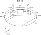
- FIG. 12 is an enlarged perspective view of the coupling line provided on the dielectric substrate.
- FIG. 13 is a plan view illustrating an operation of an angle adjustment mechanism for adjusting an orientation of the coupling line.
- FIG. 14 is a plan view illustrating a variation of a conductor-removed portion.
- FIG. 15 is a view illustrating a configuration of a directional coupler according to a second embodiment.
- FIG. 16 is a perspective view of an external appearance of the directional coupler according to the second embodiment.
- FIG. 17 is a plan view of a front surface of the dielectric substrate according to the second embodiment.
- FIG. 18 is a characteristic diagram illustrating a change in directional characteristic with respect to a width of a conductor-removed portion.
- FIG. 19 is an explanatory view of characteristics of the directional coupler.
- FIG. 21 is a characteristic diagram illustrating a frequency characteristic of an isolation characteristic.
- FIG. 22 is a characteristic diagram illustrating a frequency characteristic of a directional characteristic.
- FIG. 1 is a vertical cross-sectional view illustrating the schematic configuration of the plasma processing apparatus 1 according to the present embodiment.
- the plasma processing apparatus 1 is an apparatus configured to perform a process using a plasmarized processing gas on, for example, a semiconductor wafer W for manufacturing a semiconductor device (hereinafter, simply referred to as a “wafer”).
- a plasmarized processing gas may include a film-forming process, an etching process, and an ashing process.
- the plasma processing apparatus 1 includes a processing container 11 configured to accommodate therein the wafer W as a substrate, a stage 12 arranged inside the processing container 11 and configured to place thereon the wafer W to be processed, nozzles 23 configured to supply the processing gas into the processing container 11 , an exhaust unit 13 configured to depressurize and exhaust the interior of the processing container 11 , a microwave introduction unit 3 configured to introduce microwaves into the processing container 11 in order to generate plasma of the processing gas, and a controller 5 configured to control the respective components of the plasma processing apparatus 1 .
- the processing container 11 is formed of, for example, a metallic material, and the wafer W is loaded and unloaded through a loading and unloading port 111 provided in a side wall of the processing container 11 .
- the loading and unloading port 111 is opened and closed by a gate valve G.
- the stage 12 is disposed inside the processing container 11 , in a state of being insulated from the processing container 11 .
- the wafer W loaded into the processing container 11 is processed in a state of being placed on the stage 12 .
- a high-frequency bias power supply 41 is connected to the stage 12 via a matcher 42 .
- the high-frequency bias power supply 41 supplies high-frequency power for drawing ions into the wafer W to the stage 12 .
- the exhaust unit 13 is connected to a bottom portion of the processing container 11 via exhaust ports 112 and exhaust pipes 131 .
- the exhaust unit 13 is composed of an APC valve and a vacuum pump, and performs vacuum-evacuation such that the inner space of the processing container 11 becomes a preset pressure.
- the microwave introduction unit 3 includes a microwave output part 33 configured to generate microwaves and distribute and output the microwaves to a plurality of paths, and an antenna unit 30 configured to introduce the microwaves output from the microwave output part 33 into the processing container 11 .
- the microwave output part 33 includes a power supply 331 , a microwave oscillator 332 , an amplifier 333 configured to amplify the oscillated microwaves, and a distributor 334 configured to distribute the microwaves amplified by the amplifier 333 into the plurality of paths.
- the microwave oscillator 332 oscillates the microwaves at a predetermined frequency from 800 MHz to 1 GHz (e.g., 860 MHz).
- the frequency of the microwaves is not limited to the frequency within the above frequency range, and may be, for example, 8.35 GHz, 5.8 GHz, 2.45 GHz, or 1.98 GHz.
- the distributor 334 distributes the microwaves while matching impedances on an input side and on an output side.
- the antenna unit 30 includes a plurality of antenna modules 30 a .
- Each of the antenna modules 30 a introduces the microwaves distributed by the distributor 334 into the processing container 11 .
- the plurality of antenna modules 30 a has the same configuration.
- Each antenna module 30 a includes an amplifier part 31 configured to amplify the distributed microwaves, and a microwave introduction mechanism 32 configured to introduce the microwaves output from the amplifier part 31 into the processing container 11 .
- the amplifier part 31 includes a phase shifter 311 configured to change a phase of microwaves, a small power amplifier 312 configured to perform first-stage amplification, a driver amplifier 313 configured to adjust a power level of microwaves, a power amplifier 314 configured as a solid-state amplifier, and an isolator 315 configured to separate reflected waves of the microwaves, which are reflected by the microwave introduction mechanism 32 to be described later toward the power amplifier 314 .
- the phase shifter 311 can change a phase of microwaves so as to change radiation characteristics of the microwaves.
- the phase shifter 311 is used to change distribution of plasma by controlling directivity of the microwaves by, for example, adjusting the phase of the microwaves for each antenna module 30 a . In a case of not adjusting the radiation characteristics as described above, the phase shifter 311 may not be provided.
- the small power amplifier 312 amplifies the microwaves having the phase which has been adjusted by the phase shifter 311 with a preset gain.
- the driver amplifier 313 is used for adjusting a variation in power of the microwaves of each antenna module 30 a and adjusting an intensity of plasma. For example, a distribution of plasma in the entirety of the processing container 11 may be adjusted by changing the gain of the driver amplifier 313 for each antenna module 30 a , based on a detection result of the power level of the microwaves output from the amplifier part 31 .
- the power amplifier 314 amplifies the output of the microwaves having the power which has been adjusted by the driver amplifier 313 to a desired power level.
- the power amplifier 314 is composed of, for example, baluns (an input side and an output side), matching circuits (an input side and an output side), and a semiconductor amplification element.
- GaAs PHEMT GaAsenide Pseudomorphic High Electron Mobility Transistor
- GaAs MESFET Ga Arsenide Metal-Semiconductor Field Effect Transistor
- GaN HEMT Ga Nitride High Electron Mobility Transistor
- LDMOS Laterally-Diffused Metal-Oxide Semiconductor
- the isolator 315 has a circulator and a dummy load (a terminating resistor).
- the circulator guides reflected microwaves reflected by an antenna portion of the microwave introduction mechanism 32 , which will be described later, to the dummy load.
- the dummy load converts the reflected microwaves guided by the circulator into heat.
- a portion of the microwaves output from the amplifier part 31 having the configuration described above is extracted by using the directional coupler 6 of the present embodiment (first embodiment) to be described later, for detecting the power level.
- the directional coupler 6 may extract a portion of the traveling waves of the microwaves output from the amplifier part 31 and a portion of the reflected waves of the microwaves.
- the portion of the microwaves extracted by the directional coupler 6 is input to a power controller 316 and used as high-frequency signals for detecting a power level of each of the traveling waves and the reflected waves.
- the directional coupler 6 may extract a part of the traveling waves of the microwaves output from the amplifier part 31 and a part of the reflected waves of the microwaves.
- the part of the microwaves extracted by the directional coupler 6 is input to a power controller 316 and used as high-frequency signals for detecting a power level of each of the traveling waves and the reflected waves.
- the power controller 316 obtains the power levels of the traveling waves and reflected waves of the microwaves at the outlet of the amplifier part 31 based on signal levels of the high-frequency signals. In addition, the power controller 316 perform gain adjustment of the driver amplifier 313 and matching adjustment of the power amplifier 314 based on the detection result of the power levels.
- the microwaves output from the amplifier part 31 are input to the microwave introduction mechanism 32 .
- a configuration of the microwave introduction mechanism 32 will be described in brief with reference to FIG. 1 .
- a hollow coaxial line is constituted by a cylindrical body container 320 forming an outer conductor and an inner conductor 325 extending along a central axis of the body container 320 .
- a space between an inner peripheral surface of the body container 320 and an outer peripheral surface of the inner conductor 325 serves as a microwave transmission path.
- two annular slugs 321 formed of a dielectric material are spaced apart from each other in a vertical direction. Vertical positions of the slugs 321 are adjusted by an actuator (not illustrated) such that an impedance when the microwave introduction mechanism 32 is viewed from the amplifier part 31 becomes a predetermined value, whereby the slugs 321 serve as a tuner.
- the antenna part which includes a planar antenna 323 connected to a lower end of the inner conductor 325 , a microwave retardation member 322 arranged on a top surface of the planar antenna 323 , and a microwave transmission window 324 arranged on the bottom surface of the planar antenna 323 , are provided.
- the planar antenna 323 has a plurality of slots (openings) 323 a .
- the microwave retardation member 322 is formed of, for example, quartz, and adjusts plasma by shortening a wavelength of the microwaves.
- the microwave transmission window 324 is formed of a dielectric material such as quartz or ceramic, and closes an opening formed in the ceiling of the processing container 11 .
- the microwaves which have reached the planar antenna 323 via the microwave transmission path, penetrate the microwave transmission window 324 via the slots 323 a of the planar antenna 323 , and are radiated in a TE mode.
- the processing gas is plasmarized.
- a desired process is performed on the wafer W placed on the stage 12 by using active species (radicals and ions) generated by the plasmarization of the processing gas.
- a region below the microwave transmission window 324 in which the microwaves are radiated and plasma of the processing gas is formed, corresponds to a plasma forming part of the present embodiment.
- the respective components of the plasma processing apparatus 1 having the configuration described above are connected to the controller 5 and controlled by the controller 5 .
- the controller 5 is configured by a computer having a CPU and a storage, and controls the respective components of the plasma processing apparatus 1 .
- a program in which a group of steps (instructions) for executing operations required for processing the wafer W is set, is recorded in the storage.
- the program is stored in a storage medium such as a hard disk, a compact disk, a magneto-optical disk, or a memory card, and is installed in the computer from the storage medium.
- a portion of the microwaves output from the amplifier part 31 is extracted as high-frequency signals by the directional coupler 6 , and is used to detect the power level of the microwaves.
- FIG. 4 illustrates a schematic view of a backward-type directional coupler 60 .
- the directional coupler 60 is a device that electromagnetically couples an auxiliary line 602 to a main line 601 , through which high-frequency power flows, and extracts a portion of the high frequency power from the auxiliary line 602 as a high-frequency signal.
- reference symbol P 1 denotes an input port through which the high-frequency power is input to the main line 601
- reference symbol P 2 denotes an output port through which the high-frequency power is output from the main line 601
- P 3 is called a coupling port
- P 4 is called an isolation port.
- Reference symbols P 1 to P 4 added to the directional couplers 6 and 6 a according to the embodiments to be described later also mean the respective ports described above.
- the directional coupler 60 As the performance required for the directional coupler 60 , it is preferable that high-frequency power having a required level can be extracted from the coupling port P 3 and components of traveling waves leaking to the isolation port P 4 is small. That is, the directional coupler 60 is required to have a large value of the directional characteristic S 31 -S 41 while having a value of the coupling characteristic S 31 within a preset target range.
- the power level of the microwaves output from each amplifier part 31 is several hundred watts. In this case, it is sufficient to obtain a small amount of electric power for microwave monitoring.
- the directional coupler 6 is designed such that the coupling characteristic S 31 ⁇ 30 dB is satisfied, for example.
- the electromagnetic coupling state between the main line 601 and the auxiliary line 602 (a coupling line 68 to be described later) needs to be a loosely-coupled state.
- the loosely-coupled directional coupler 60 has a problem in that it is difficult to improve the directional characteristic thereof.
- the directional coupler 6 of the present embodiment has a configuration capable of improving the directional characteristic while loosely coupling the coupling line 68 as the auxiliary line 602 to a central conductor 61 as the main line 601 .
- FIG. 5 is an exploded perspective view of the directional coupler 6
- FIG. 6 is a vertical cross-sectional view of the directional coupler 6 when viewed from a front side
- FIG. 7 is a vertical cross-sectional view of the directional coupler 6 when viewed from a lateral side.
- sides of the base end and tip end of the Y-axis arrow of the X-Y-Z coordinate system indicated in FIG. 5 are also referred to as a front side and a rear side, respectively.
- the directional coupler 6 of the present embodiment includes a hollow coaxial line composed of the central conductor 61 forming the main line 601 and an outer conductor 62 provided to surround the central conductor 61 , a dielectric substrate 65 provided with the coupling line 68 forming the auxiliary line 602 , and a metallic spacer 64 for adjusting a distance between the central conductor 61 and the coupling line 68 .
- the outer conductor 62 is configured by, for example, a rectangular parallelepiped housing formed of a conductive metal.
- a cylindrical space (a cylindrical space 620 ) into which the central conductor 61 can be inserted is formed in a region extending from a front side surface to a rear side surface of the outer conductor 62 .
- a recess capable of accommodating the metallic spacer 64 and the dielectric substrate 65 is formed in a top surface of the outer conductor 62 .
- a bottom surface in the recess is flat, and the dielectric substrate 65 is mounted on the flat surface, with a circular opening 641 interposed therebetween. From this point of view, the flat surface in the recess corresponds to a substrate-mounting portion 63 of the present embodiment.
- the substrate-mounting portion 63 has a rectangular square opening 631 that is open toward the cylindrical space 620 when viewed from above.
- a long side direction of the square opening 631 corresponds to a transmission direction of the microwaves.
- a length of the square opening 631 in the long side direction is set to be, for example, ⁇ 0 /10 with respect to a free space wavelength ⁇ 0 of the microwaves.
- ⁇ 0 is calculated from a frequency of the microwaves f [Hz] and the speed of light c 0 [m/s] by using Equation (6) as follows.
- ⁇ 0 c 0 /f [ m ] (6)
- m is a meter as a unit length of the free space wavelength ⁇ 0 .
- the central conductor 61 is configured by, for example, a round bar-shaped member (rod-shaped conductor) formed of a conductive metal. As illustrated in FIG. 6 , a diameter of the central conductor 61 is smaller than a diameter of the cylindrical space 620 formed on the side of the outer conductor 62 . The central conductor 61 is inserted into the cylindrical space 620 and is arranged such that positions of central axes of both the central conductor 61 and the cylindrical space 620 are aligned.
- the central conductor 61 is held by insulating members 621 , which are provided so as to be fitted into openings formed in both the front and rear surfaces of the outer conductor 62 , respectively.
- An input side coaxial connector (input terminal) 69 a and an output side coaxial connector (output terminal) 69 b are provided on the front side surface and the rear side surface of the outer conductor 62 , respectively.
- the central conductor portion 693 is connected to the central conductor 61
- the outer peripheral conductor portion 691 is connected to the outer conductor 62 .
- the input side coaxial connector 69 a corresponds to the input port P 1 of the directional coupler 6 , and is connected to a side of an outlet of the amplifier part 31 .
- the output side coaxial connector 69 b corresponds to the output port P 2 , and is connected to a side of an inlet of the microwave introduction mechanism 32 (see FIG. 2 ).
- the metallic spacer 64 is configured by a rectangular conductive metallic plate.
- the metallic spacer 64 is configured to have a size that can be accommodated in the recess formed on the top surface of the outer conductor 62 , and the circular opening 641 is formed in the central portion thereof.
- the circular opening 641 is in communication with the cylindrical space 620 via the square opening 631 formed in the substrate-mounting portion 63 of the outer conductor 62 .
- the metallic spacer 64 serves to adjust the coupling characteristic of the directional coupler 6 by adjusting the distance between the central conductor 61 and the coupling line 68 .
- the metallic spacer 64 may have a thickness dimension within a range of 0.5 mm to 2 mm depending on the frequency of microwaves or the like.
- the dielectric substrate 65 is a rectangular plate formed of, for example, epoxy glass, a fluororesin such as polytetrafluoroethylene (PTFE), and a dielectric material such as alumina.
- the dielectric substrate 65 is configured to have a size that can be accommodated in the recess formed in the top surface of the outer conductor 62 .
- the dielectric substrate 65 is arranged on the substrate-mounting portion 63 (on the metallic spacer 64 ) to cover the square opening 631 and the circular opening 641 described above (see FIG. 10 ).
- the metallic spacer 64 and the dielectric substrate 65 are provided with screw holes 642 and 651 , respectively, at a plurality of locations.
- substrate-fixing screws 66 By inserting substrate-fixing screws 66 into the screw holes 642 and 651 and screw-coupling the substrate-fixing screws 66 to female screws 632 provided in the substrate-mounting portion 63 , the metallic spacer 64 and the dielectric substrate 65 are fastened to the substrate-mounting portion 63 .
- a surface (bottom surface) of the dielectric substrate 65 facing the central conductor 61 via the circular opening 641 and the square opening 631 is referred to as a “rear surface” of the dielectric substrate 65
- an opposite surface (top surface) thereof is referred to as a “front surface” of the dielectric substrate 65 .
- Film-shaped ground conductors (a front surface conductor (a ground conductor on the side of the front surface) 652 (see FIG. 8 ) and a rear surface conductor (a ground conductor on the side of the rear surface) 656 (see FIG. 9 )) formed of, for example, a copper foil are provided on the front surface and the rear surface of the dielectric substrate 65 , respectively.
- FIG. 8 is a plan view of the front surface of the dielectric substrate 65 viewed from above
- FIG. 9 is a plan view of the rear surface of the dielectric substrate 65 viewed through the dielectric substrate 65 from above.
- the front surface conductor 652 and the rear surface conductor 656 are arranged so as to cover the substantially entirety of both the front and rear surfaces of the dielectric substrate 65 . As illustrated in FIG. 8 , a large number of through-holes 653 are distributedly formed over the plate surface of the dielectric substrate 65 .
- the front surface conductor 652 and the rear surface conductor 656 are electrically connected to each other via connecting lines (not illustrated) formed along the respective through-holes 653 .
- connecting one or both of the front surface conductor 652 and the rear surface conductor 656 to the outer conductor 62 via the substrate-fixing screws 66 ( FIG. 5 ) both the front surface conductor 652 and the rear surface conductor 656 are grounded.
- the outer conductor 62 is grounded via a ground line (not illustrated).
- the coupling line 68 is provided at a location facing the central conductor 61 in the cylindrical space 620 via the above-described square opening 631 and circular opening 641 .
- the coupling line 68 corresponds to the auxiliary line 602 of the directional coupler 6 of the present embodiment.
- the coupling line 68 is configured by, for example, a copper foil as a conductor film.
- the coupling line 68 may be formed by forming a copper foil on the entirety of the rear surface of the dielectric substrate 65 by plating, and then removing a portion of the copper foil around the coupling line 68 by etching to provide a separation region 650 b between the rear surface conductor 656 and the coupling line 68 . Therefore, the coupling line 68 is in an electrically non-conductive state with (a state of not being electrically connected to) the rear surface conductor 656 .
- the coupling line 68 is formed in an elongated strip shape.
- a length of the coupling line 68 in the long side direction is set to ⁇ g /4 or less, specifically, ⁇ g /20 or less, with respect to a wavelength ⁇ g of the microwaves on the dielectric substrate 65 .
- ⁇ g is calculated by using the following Equation (7), based on the above-mentioned free space wavelength ⁇ 0 of the microwaves and an effective dielectric constant ⁇ eff of the dielectric substrate 65 .
- ⁇ g ⁇ 0 /( ⁇ eff ) 0.5 [ m ] (7)
- ⁇ eff can be obtained from, for example, formulas described in a literature (T. C. Edwards, M. B. Steer, Foundations for Microstrip Circuit Design, 4 th Edition, pp. 127-134, John Wiley & Sons, Inc., 2016).
- FIGS. 10 and 11 dimensions in the long side direction w and a short side direction d of the coupling line 68 as shown in FIG. 11 are set such that the coupling line 68 is included in an opening region formed by overlapping the square opening 631 in the substrate-mounting portion 63 with the circular opening 641 in the metallic spacer 64 .
- FIGS. 10 and 11 illustrate states seen through a dielectric main body, the front surface conductor 652 , the rear surface conductor 656 of the dielectric substrate 65 , and the like.
- FIG. 11 shows an arrangement direction of the coupling line 68 when viewed from above, which is opposite to the surface of the coupling line 68 .
- Line B-B′ in FIG. 11 coincides with an extending direction of the central conductor 61 arranged inside the outer conductor 62 while line A-A′ is orthogonal to the line B-B′ as shown in FIG. 10 .
- the coupling line 68 is arranged such that an extending direction of the elongated strip-shaped coupling line 68 and the extending direction of the central conductor 61 (the direction of line B-B′ in FIG. 11 ) intersect with each other at an angle ⁇ when viewed from above.
- the intersection angle ⁇ is a parameter that affects the directional characteristic of the directional coupler 6 .
- the intersection angle ⁇ is set to be, for example, a preset angle within a range of 39 ⁇ 2 degrees.
- intersection angle ⁇ may be set when designing the coupling line 68 on the rear surface of the dielectric substrate 65 .
- the intersection angle ⁇ may be adjusted by changing a mounting direction of the dielectric substrate 65 with respect to the outer conductor 62 when viewed from above.
- FIG. 13 illustrates an exemplary configuration of an angle adjustment mechanism for adjusting the mounting direction of the dielectric substrate 65 .
- the angle adjustment mechanism of the present embodiment is composed of the substrate-fixing screws 66 for attaching the dielectric substrate 65 to the substrate-mounting portion 63 , and the screw holes 651 formed to be wider than the diameter of the substrate-fixing screws 66 in an angle adjustment direction of the dielectric substrate 65 .
- the screw holes 651 By forming the screw holes 651 to have enough room with respect to the diameter of the substrate-fixing screws 66 and changing the mounting direction of the dielectric substrate 65 as illustrated in FIG. 13 , it is possible to adjust the intersection angle ⁇ described above with reference to FIG. 11 .
- the coupling line 68 is formed on the flat rear surface of the dielectric substrate 65 as a plate member. With this configuration, when viewed from a direction along the surface of the dielectric substrate 65 as illustrated in FIG. 7 , the extending direction of the central conductor 61 and the extending direction of the coupling line 68 are aligned (substantially parallel to each other).
- a coaxial connector 67 a for traveling waves (a traveling wave extraction terminal) configured to extract a portion of the traveling waves of the microwaves via the coupling line 68 ( FIG. 9 )
- a coaxial connector 67 b for reflected waves (a reflected wave extraction terminal) configured to extract a portion of the reflected waves of the microwaves
- the coaxial connector 67 a for traveling waves corresponds to the coupling port P 3 of the directional coupler 6
- the coaxial connector 67 b for reflected waves corresponds to the isolation port P 4 of the directional coupler 6 .
- each of the connectors 67 a and 67 b is connected to a signal line that outputs a portion of the microwaves as a high-frequency signal toward the power controller 316 (see FIG. 3 ).
- the coaxial connector 67 a for traveling waves and the coaxial connector 67 b for reflected waves are connected to one end of an extraction line 655 a and one end of an extraction line 655 b , which are formed on the side of the front surface of the dielectric substrate 65 , respectively.
- Each of the extraction lines 655 a and 655 b is formed with a gap with respect to the front surface conductor 652 via a separation region 650 a .
- the extraction lines 655 a and 655 b may be formed, for example, by forming a copper foil on the entirety of the front surface of the dielectric substrate 65 by plating, and then removing portions of the copper foil around the extraction lines 655 a and 655 b by etching, respectively, to provide the separation regions 650 a between the front surface conductor 652 and the extraction line 655 a and between the front surface conductor 652 and the extraction line 655 b.
- each of the extraction lines 655 a and 655 b constitutes a grounded coplanar line having a characteristic impedance of 50 ⁇ between the front surface conductor 652 , which is provided in regions on both sides of the extraction lines 655 a and 655 b , and the rear surface conductor 656 .
- the width of the separation regions 650 a may be increased to such an extent that the effect of the electromagnetic field of the front surface conductor 652 becomes sufficiently small by further cutting out portions of the front surface conductor 652 in the regions on both sides of the extraction lines 655 a and 655 b .
- the width of the separation regions 650 a in this case needs to be equal to or greater than a thickness of the dielectric substrate 65 , whereby each of the extraction lines 655 a and 655 b constitutes a microstrip line with the rear surface conductor 656 .
- the other ends of the extraction lines 655 a and 655 b extend to locations corresponding to opposite ends of the coupling line 68 in the long side direction, respectively, and are connected to the coupling line 68 on the rear surface via through holes 654 a and 654 b formed in the dielectric substrate 65 at the above-described locations, respectively.
- the central conductor 61 as the main line 601 and the coupling line 68 as the auxiliary line 602 are electromagnetically coupled to each other.
- a portion of the traveling waves of the microwaves can be extracted as a high-frequency signal from the coaxial connector 67 a for traveling waves, which is the coupling port P 3 .
- a portion of the reflected waves of the microwaves can be extracted as a high-frequency signal from the coaxial connector 67 b for reflected waves, which is the isolation port P 4 .
- the directional coupler 6 of the present embodiment improves the directional characteristic by providing the following configurations.
- the front surface conductor 652 is provided with a conductor-removed portion (a non-conductive region) 67 in which a portion of the copper foil (a conductor film) in a region (a counterpart region) facing the coupling line 68 via the dielectric substrate 65 is removed.
- the perspective view of FIG. 12 illustrates a state viewed through the dielectric substrate 65 , the front surface conductor 652 , and the rear surface conductor 656 , other than the counterpart region.
- a shape of the conductor-removed portion 67 is not particularly limited.
- the square conductor-removed portion 67 may be provided as illustrated in FIG. 11 , or a rectangular or circular conductor-removed portion 67 ′ or 67 ′′ may be provided as illustrated in FIG. 14 .
- the number of conductor-removed portions 67 formed on the front surface conductor 652 is not limited to one, and a plurality of conductor-removed portions 67 may be provided.
- the dimensions, shapes, arrangement number, and arrangement positions of conductor-removed portions 67 are determined by combining the dimensions, shapes, arrangement number, and arrangement positions with other design parameters such as the opening length of the square opening 631 , the opening diameter of the circular opening 641 , the length of the coupling line 68 in the long side direction, and the intersection angle ⁇ , and searching for conditions that can exhibit suitable directional characteristics through simulations and trial tests.
- elements that perform a wave processing on microwaves to be extracted are provided in the extraction line 655 a from the coupling line 68 to the coaxial connector 67 a for traveling waves and in the extraction line 655 b from the coupling line 68 to the coaxial connector 67 b for reflected microwaves.
- the LPF 72 and HPF 73 may be configured by band-pass filters (BPFs) having the same frequency characteristics.
- the attenuators 71 , the LPF 72 , and the HPF 73 are provided for the extraction lines 655 a and 655 b in this order from the side of the coupling line 68 to the sides of the connectors 67 a and 67 b , respectively.
- these elements may be arranged on side of the front surface of the dielectric substrate 65 .
- Combination of the elements provided on the extraction lines 655 a and 655 b is not limited to the above-described example, and may be appropriately selected depending on the purpose of use of the high-frequency signals and the like.
- the directional coupler 6 or 6 a having a good directional characteristic while loosely coupling the coupling line 68 as the auxiliary line 602 to the central conductor 61 as the main line 601 .
- FIGS. 11 and 12 illustrate an example in which the diameter of the circular opening 641 formed in the metallic spacer 64 is larger than the dimension of the square opening 631 formed in the substrate-mounting portion 63 in the short side direction.
- a magnitude relationship between these dimensions is not limited to the example illustrated in FIGS. 11 and 12 .
- the diameter of the circular opening 641 formed in the metallic spacer 64 may be smaller than the dimension of the square opening 631 formed in the substrate-mounting portion 63 in the short side direction.
- the shape of the opening viewed from above is circular. It is not an essential requirement to dispose the metallic spacer 64 between the substrate-mounting portion 63 and the dielectric substrate 65 , and the dielectric substrate 65 may be disposed directly on the substrate-mounting portion 63 . In this case, the substrate-mounting portion 63 may be provided with a circular opening.
- the coupling line 68 is arranged so as to face the central conductor 61 via the circular opening 641 as illustrated in FIG. 14 , the distance from each location on the coupling line 68 to the periphery of the circular opening 641 does not change even if the intersection angle ⁇ is changed by using the angle adjustment mechanism described above with reference to FIG. 13 .
- the dielectric substrate 65 is not limited to be configured using a two-layer substrate in which ground conductors (the front surface conductor 652 and the rear surface conductor 656 ) are formed only on both the front and rear surfaces of the dielectric substrate 65 .
- the dielectric substrate 65 may be configured using a multilayer substrate having three or more layers, in which one or more layers of ground conductors are inserted in the dielectric substrate 65 in addition to the ground conductors on both the front and rear surfaces thereof.
- the installation position of the directional coupler 6 or 6 a described above is not limited to the location between the amplifier part 31 and the microwave introduction mechanism 32 as described above with reference to FIG. 2 .
- the directional coupler 6 or 6 a may be provided at a required position in the microwave supply path from the microwave oscillator 332 ( FIG. 2 ) as a microwave supplier to a region below the microwave transmission window 324 ( FIG. 1 ) as the plasma forming part.
- the directional coupler 6 or 6 a such that the inner conductor 325 of the microwave introduction mechanism 32 serves as the central conductor 61 , a portion of microwaves flowing through the microwave introduction mechanism 32 may be extracted.
- a simulation model based on the directional coupler 6 illustrated in FIG. 7 was fabricated, and evaluation indices of the directional coupler 6 were obtained.
- a central conductor 61 having a diameter of 12 mm and a length of 43 mm was disposed in an outer conductor 62 in which a cylindrical space 620 having a diameter of 28 mm was formed, and a dielectric substrate 65 was provided on a substrate-mounting portion 63 , in which a square opening 631 having a length of 33 mm in the long side direction was formed, with a metallic spacer 64 , in which a circular opening 641 having a diameter of 26 mm is formed, being interposed therebetween.
- the length of the coupling line 68 in the long side direction was 8 mm, and the length thereof in the short side direction was 2.6 mm.
- the thickness of the metallic spacer 64 was 1.5 mm, and the height distance between the central conductor 61 and the coupling line 68 was 15.5 mm from the center of the central conductor 61 .
- the intersection angle ⁇ was set to 43 degrees.
- a square conductor-removed portion 67 in which the length of each side (the width of the conductor-removed portion) was d, was provided at a location facing the center of the coupling line 68 .
- a coupling characteristic, an isolation characteristic, and a directional characteristic were obtained by inputting microwaves having a predetermined frequency to the input port P 1 .
- Various frequency characteristics were calculated by using a simulator of HFSS (trademark) from ANSYS (registered mark).
- FIG. 18 shows a change in the directional characteristic dB when microwaves of 860 MHz were supplied to the simulation model of each of Example 1-1 to 1-6.
- the coupling characteristic and the isolation characteristic i.e. each in dB
- the coupling characteristics in dB obtained by changing the frequencies in MHz of the signals supplied to the directional coupler 6 were compared, and the result is shown in FIG. 20 .
- the isolation characteristics in dB obtained by changing the frequencies in MHz of the signals supplied to the directional coupler 6 were compared, and the result is shown in FIG. 21 .
- the directional characteristics in dB obtained by changing the frequencies in MHz of the signals supplied to the directional coupler 6 were compared, and the result is shown in FIG. 22 .
- the coupling characteristic does not depend on the width of the conductor-removed portion 67 and is constant and equivalent among Examples 1-4 to 1-6.
- the isolation characteristic changes among Examples 1-4 to 1-6 in response to the change in the width (i.e. from 2.0 mm to 2.5 mm to 3.0 mm) of the conductor-removed portion 67 .
- the coupling characteristic is substantially not changed (while maintaining the loosely coupled state), and only the isolation characteristic changes.
- the directional characteristic can be improved depending on the width of the conductor-removed portion being changed (i.e. from 2.0 mm to 2.5 mm to 3.0 mm).
- a directional coupler 6 having almost the same configuration as the simulation model set in Simulation 1 was fabricated, and a directional characteristic of the directional coupler 6 was obtained by using a vector network analyzer.
- the test result is shown in FIG. 23 .
- FIG. 23 in each of Examples 2-1 to 2-3, it was confirmed that when the intersection angle ⁇ is changed was changed, the directional characteristic in dB was also changed. Therefore, it was confirmed that it is possible to obtain a directional coupler 6 having the more suitable directional characteristic by combining the width of the conductor-removed portion 67 and the intersection angle ⁇ .
- the directional characteristic of the directional coupler of Comparative Example 2-1 in which no conductor-removed portion 67 was provided, was in the vicinity of ⁇ 20 dB.
- the directional characteristics were ⁇ 30 dB or less (30 dB or more in absolute value) for widths of 2.3 mm, 2.5 mm and 2.7 mm, and thus good performance was obtained.
- the directional characteristic of the directional coupler 6 can be improved by providing the conductor-removed portion 67 by removing a portion of the conductor film in the region facing the coupling line 68 via the dielectric substrate 65 .
- a good directional characteristic of a directional coupler while loosely coupling a coupling line, which is an auxiliary line of the directional coupler, to a central conductor, which is a main line of the directional coupler.
Landscapes
- Physics & Mathematics (AREA)
- Engineering & Computer Science (AREA)
- Plasma & Fusion (AREA)
- Chemical & Material Sciences (AREA)
- Analytical Chemistry (AREA)
- Electromagnetism (AREA)
- Spectroscopy & Molecular Physics (AREA)
- Plasma Technology (AREA)
- Optical Integrated Circuits (AREA)
Applications Claiming Priority (3)
| Application Number | Priority Date | Filing Date | Title |
|---|---|---|---|
| JP2020012640A JP7331717B2 (ja) | 2020-01-29 | 2020-01-29 | 方向性結合器、基板を処理する装置、及び基板を処理する方法 |
| JPJP2020-012640 | 2020-01-29 | ||
| JP2020-012640 | 2020-01-29 |
Publications (2)
| Publication Number | Publication Date |
|---|---|
| US20210234248A1 US20210234248A1 (en) | 2021-07-29 |
| US11569558B2 true US11569558B2 (en) | 2023-01-31 |
Family
ID=76970614
Family Applications (1)
| Application Number | Title | Priority Date | Filing Date |
|---|---|---|---|
| US17/155,618 Active 2041-04-11 US11569558B2 (en) | 2020-01-29 | 2021-01-22 | Directional coupler for use in a substrate processing apparatus, where the directional coupler includes a coaxial line coupled to a conductor on a substrate |
Country Status (4)
| Country | Link |
|---|---|
| US (1) | US11569558B2 (ja) |
| JP (1) | JP7331717B2 (ja) |
| KR (1) | KR102465595B1 (ja) |
| CN (1) | CN113193324B (ja) |
Citations (2)
| Publication number | Priority date | Publication date | Assignee | Title |
|---|---|---|---|---|
| JP2003032013A (ja) | 2001-07-11 | 2003-01-31 | Matsushita Electric Ind Co Ltd | 方向性結合器 |
| US20090045887A1 (en) * | 2006-02-28 | 2009-02-19 | Powerwave Comtek Oy | Directional coupler |
Family Cites Families (12)
| Publication number | Priority date | Publication date | Assignee | Title |
|---|---|---|---|---|
| JPH06310918A (ja) * | 1993-04-23 | 1994-11-04 | Toshiba Corp | 真空気密型方向性結合器 |
| JP3498597B2 (ja) * | 1998-10-22 | 2004-02-16 | 株式会社村田製作所 | 誘電体線路変換構造、誘電体線路装置、方向性結合器、高周波回路モジュールおよび送受信装置 |
| JP2003204203A (ja) * | 2002-01-08 | 2003-07-18 | Murata Mfg Co Ltd | 方向性結合器付きフィルタおよび通信装置 |
| KR100500360B1 (ko) * | 2002-01-26 | 2005-07-12 | 고등기술연구원연구조합 | 고효율 상압 마이크로웨이브 플라즈마시스템 |
| JP3822857B2 (ja) | 2002-10-29 | 2006-09-20 | 長野日本無線株式会社 | プラズマ発生方法、プラズマ装置および半導体製造装置 |
| US7183876B2 (en) | 2003-04-04 | 2007-02-27 | Electronics Research, Inc. | Variable coupling factor directional coupler |
| US7088201B2 (en) | 2004-08-04 | 2006-08-08 | Eudyna Devices Inc. | Three-dimensional quasi-coplanar broadside microwave coupler |
| JP2010239534A (ja) | 2009-03-31 | 2010-10-21 | Maspro Denkoh Corp | 方向性結合器 |
| JP5435309B2 (ja) | 2011-08-25 | 2014-03-05 | Tdk株式会社 | 方向性結合器および無線通信装置 |
| KR102009541B1 (ko) * | 2012-02-23 | 2019-08-09 | 도쿄엘렉트론가부시키가이샤 | 플라즈마 처리 장치, 및 고주파 발생기 |
| JP6048700B2 (ja) * | 2015-02-24 | 2016-12-21 | Tdk株式会社 | 方向性結合器および無線通信装置 |
| DE102019100337A1 (de) | 2019-01-08 | 2020-07-09 | Rohde & Schwarz GmbH & Co. Kommanditgesellschaft | Richtkoppler, Verfahren zur Herstellung eines Richtkopplers sowie Baukastensystem |
-
2020
- 2020-01-29 JP JP2020012640A patent/JP7331717B2/ja active Active
-
2021
- 2021-01-19 KR KR1020210007487A patent/KR102465595B1/ko active IP Right Grant
- 2021-01-19 CN CN202110067295.4A patent/CN113193324B/zh active Active
- 2021-01-22 US US17/155,618 patent/US11569558B2/en active Active
Patent Citations (2)
| Publication number | Priority date | Publication date | Assignee | Title |
|---|---|---|---|---|
| JP2003032013A (ja) | 2001-07-11 | 2003-01-31 | Matsushita Electric Ind Co Ltd | 方向性結合器 |
| US20090045887A1 (en) * | 2006-02-28 | 2009-02-19 | Powerwave Comtek Oy | Directional coupler |
Also Published As
| Publication number | Publication date |
|---|---|
| US20210234248A1 (en) | 2021-07-29 |
| KR102465595B1 (ko) | 2022-11-10 |
| KR20210097026A (ko) | 2021-08-06 |
| CN113193324B (zh) | 2022-05-31 |
| CN113193324A (zh) | 2021-07-30 |
| JP7331717B2 (ja) | 2023-08-23 |
| JP2021118513A (ja) | 2021-08-10 |
Similar Documents
| Publication | Publication Date | Title |
|---|---|---|
| KR102007059B1 (ko) | 플라즈마 발생용 안테나, 플라즈마 처리 장치 및 플라즈마 처리 방법 | |
| JP5368514B2 (ja) | プラズマ処理装置 | |
| US7102292B2 (en) | Method and device for removing harmonics in semiconductor plasma processing systems | |
| US9702913B2 (en) | Acquisition method for S-parameters in microwave introduction modules, and malfunction detection method | |
| US8384492B2 (en) | Coaxial line to microstrip connector having slots in the microstrip line for receiving an encircling metallic plate | |
| US10826152B2 (en) | Broadband radio frequency coupler | |
| US10991549B2 (en) | Antenna and plasma deposition apparatus | |
| KR20110018431A (ko) | 플라즈마 처리장치 | |
| JP4099074B2 (ja) | プラズマ処理装置およびプラズマ処理方法 | |
| US11233303B2 (en) | High frequency filter | |
| US11569558B2 (en) | Directional coupler for use in a substrate processing apparatus, where the directional coupler includes a coaxial line coupled to a conductor on a substrate | |
| US7595707B2 (en) | Microstripline type directional coupler and communication device using the same | |
| Neininger et al. | 16-way Ka-band power combiner using novel waveguide transitions | |
| US20210110999A1 (en) | Plasma processing apparatus | |
| WO2020014891A1 (en) | Balun and method for manufacturing the same | |
| KR20070075936A (ko) | Sir형 밴드패스필터 | |
| US20240170256A1 (en) | VHF Broadband Coaxial Adapter | |
| Evseev et al. | Contact device with tunable strip matching circuits for measuring parameters of microwave transistors | |
| US10591571B1 (en) | Adjustable pre-matching coaxial transistor test fixture | |
| JP2008135883A (ja) | 高周波電力モニタ回路 | |
| JP3958578B2 (ja) | プラズマ処理装置 | |
| KR20170084397A (ko) | 광대역 특성을 갖는 소형 rf 신호 결합기 |
Legal Events
| Date | Code | Title | Description |
|---|---|---|---|
| FEPP | Fee payment procedure |
Free format text: ENTITY STATUS SET TO UNDISCOUNTED (ORIGINAL EVENT CODE: BIG.); ENTITY STATUS OF PATENT OWNER: LARGE ENTITY |
|
| AS | Assignment |
Owner name: TOKYO ELECTRON LIMITED, JAPAN Free format text: ASSIGNMENT OF ASSIGNORS INTEREST;ASSIGNORS:TAKAHASHI, ISAO;MIYASHITA, HIROYUKI;OSADA, YUKI;AND OTHERS;REEL/FRAME:055064/0347 Effective date: 20210105 |
|
| STPP | Information on status: patent application and granting procedure in general |
Free format text: APPLICATION DISPATCHED FROM PREEXAM, NOT YET DOCKETED |
|
| STPP | Information on status: patent application and granting procedure in general |
Free format text: DOCKETED NEW CASE - READY FOR EXAMINATION |
|
| STPP | Information on status: patent application and granting procedure in general |
Free format text: NON FINAL ACTION MAILED |
|
| STPP | Information on status: patent application and granting procedure in general |
Free format text: RESPONSE TO NON-FINAL OFFICE ACTION ENTERED AND FORWARDED TO EXAMINER |
|
| STPP | Information on status: patent application and granting procedure in general |
Free format text: NOTICE OF ALLOWANCE MAILED -- APPLICATION RECEIVED IN OFFICE OF PUBLICATIONS |
|
| STPP | Information on status: patent application and granting procedure in general |
Free format text: PUBLICATIONS -- ISSUE FEE PAYMENT RECEIVED |
|
| STCF | Information on status: patent grant |
Free format text: PATENTED CASE |