US11437552B2 - Semiconductor device with transmissive layer and manufacturing method thereof - Google Patents
Semiconductor device with transmissive layer and manufacturing method thereof Download PDFInfo
- Publication number
- US11437552B2 US11437552B2 US17/026,752 US202017026752A US11437552B2 US 11437552 B2 US11437552 B2 US 11437552B2 US 202017026752 A US202017026752 A US 202017026752A US 11437552 B2 US11437552 B2 US 11437552B2
- Authority
- US
- United States
- Prior art keywords
- component
- layer
- conductive
- redistribution structure
- semiconductor device
- Prior art date
- Legal status (The legal status is an assumption and is not a legal conclusion. Google has not performed a legal analysis and makes no representation as to the accuracy of the status listed.)
- Active, expires
Links
Images


Classifications
-
- H—ELECTRICITY
- H01—ELECTRIC ELEMENTS
- H01L—SEMICONDUCTOR DEVICES NOT COVERED BY CLASS H10
- H01L21/00—Processes or apparatus adapted for the manufacture or treatment of semiconductor or solid state devices or of parts thereof
- H01L21/02—Manufacture or treatment of semiconductor devices or of parts thereof
- H01L21/04—Manufacture or treatment of semiconductor devices or of parts thereof the devices having at least one potential-jump barrier or surface barrier, e.g. PN junction, depletion layer or carrier concentration layer
- H01L21/50—Assembly of semiconductor devices using processes or apparatus not provided for in a single one of the subgroups H01L21/06 - H01L21/326, e.g. sealing of a cap to a base of a container
- H01L21/56—Encapsulations, e.g. encapsulation layers, coatings
- H01L21/563—Encapsulation of active face of flip-chip device, e.g. underfilling or underencapsulation of flip-chip, encapsulation preform on chip or mounting substrate
-
- H—ELECTRICITY
- H01—ELECTRIC ELEMENTS
- H01L—SEMICONDUCTOR DEVICES NOT COVERED BY CLASS H10
- H01L33/00—Semiconductor devices with at least one potential-jump barrier or surface barrier specially adapted for light emission; Processes or apparatus specially adapted for the manufacture or treatment thereof or of parts thereof; Details thereof
- H01L33/48—Semiconductor devices with at least one potential-jump barrier or surface barrier specially adapted for light emission; Processes or apparatus specially adapted for the manufacture or treatment thereof or of parts thereof; Details thereof characterised by the semiconductor body packages
- H01L33/58—Optical field-shaping elements
-
- H—ELECTRICITY
- H01—ELECTRIC ELEMENTS
- H01L—SEMICONDUCTOR DEVICES NOT COVERED BY CLASS H10
- H01L24/00—Arrangements for connecting or disconnecting semiconductor or solid-state bodies; Methods or apparatus related thereto
- H01L24/01—Means for bonding being attached to, or being formed on, the surface to be connected, e.g. chip-to-package, die-attach, "first-level" interconnects; Manufacturing methods related thereto
- H01L24/18—High density interconnect [HDI] connectors; Manufacturing methods related thereto
- H01L24/19—Manufacturing methods of high density interconnect preforms
-
- H—ELECTRICITY
- H01—ELECTRIC ELEMENTS
- H01L—SEMICONDUCTOR DEVICES NOT COVERED BY CLASS H10
- H01L21/00—Processes or apparatus adapted for the manufacture or treatment of semiconductor or solid state devices or of parts thereof
- H01L21/67—Apparatus specially adapted for handling semiconductor or electric solid state devices during manufacture or treatment thereof; Apparatus specially adapted for handling wafers during manufacture or treatment of semiconductor or electric solid state devices or components ; Apparatus not specifically provided for elsewhere
- H01L21/683—Apparatus specially adapted for handling semiconductor or electric solid state devices during manufacture or treatment thereof; Apparatus specially adapted for handling wafers during manufacture or treatment of semiconductor or electric solid state devices or components ; Apparatus not specifically provided for elsewhere for supporting or gripping
- H01L21/6835—Apparatus specially adapted for handling semiconductor or electric solid state devices during manufacture or treatment thereof; Apparatus specially adapted for handling wafers during manufacture or treatment of semiconductor or electric solid state devices or components ; Apparatus not specifically provided for elsewhere for supporting or gripping using temporarily an auxiliary support
-
- H—ELECTRICITY
- H01—ELECTRIC ELEMENTS
- H01L—SEMICONDUCTOR DEVICES NOT COVERED BY CLASS H10
- H01L21/00—Processes or apparatus adapted for the manufacture or treatment of semiconductor or solid state devices or of parts thereof
- H01L21/70—Manufacture or treatment of devices consisting of a plurality of solid state components formed in or on a common substrate or of parts thereof; Manufacture of integrated circuit devices or of parts thereof
- H01L21/71—Manufacture of specific parts of devices defined in group H01L21/70
- H01L21/768—Applying interconnections to be used for carrying current between separate components within a device comprising conductors and dielectrics
-
- H—ELECTRICITY
- H01—ELECTRIC ELEMENTS
- H01L—SEMICONDUCTOR DEVICES NOT COVERED BY CLASS H10
- H01L23/00—Details of semiconductor or other solid state devices
- H01L23/28—Encapsulations, e.g. encapsulating layers, coatings, e.g. for protection
- H01L23/31—Encapsulations, e.g. encapsulating layers, coatings, e.g. for protection characterised by the arrangement or shape
-
- H—ELECTRICITY
- H01—ELECTRIC ELEMENTS
- H01L—SEMICONDUCTOR DEVICES NOT COVERED BY CLASS H10
- H01L23/00—Details of semiconductor or other solid state devices
- H01L23/48—Arrangements for conducting electric current to or from the solid state body in operation, e.g. leads, terminal arrangements ; Selection of materials therefor
-
- H—ELECTRICITY
- H01—ELECTRIC ELEMENTS
- H01L—SEMICONDUCTOR DEVICES NOT COVERED BY CLASS H10
- H01L23/00—Details of semiconductor or other solid state devices
- H01L23/52—Arrangements for conducting electric current within the device in operation from one component to another, i.e. interconnections, e.g. wires, lead frames
-
- H—ELECTRICITY
- H01—ELECTRIC ELEMENTS
- H01L—SEMICONDUCTOR DEVICES NOT COVERED BY CLASS H10
- H01L24/00—Arrangements for connecting or disconnecting semiconductor or solid-state bodies; Methods or apparatus related thereto
-
- H—ELECTRICITY
- H01—ELECTRIC ELEMENTS
- H01L—SEMICONDUCTOR DEVICES NOT COVERED BY CLASS H10
- H01L24/00—Arrangements for connecting or disconnecting semiconductor or solid-state bodies; Methods or apparatus related thereto
- H01L24/01—Means for bonding being attached to, or being formed on, the surface to be connected, e.g. chip-to-package, die-attach, "first-level" interconnects; Manufacturing methods related thereto
- H01L24/18—High density interconnect [HDI] connectors; Manufacturing methods related thereto
- H01L24/20—Structure, shape, material or disposition of high density interconnect preforms
-
- H—ELECTRICITY
- H01—ELECTRIC ELEMENTS
- H01L—SEMICONDUCTOR DEVICES NOT COVERED BY CLASS H10
- H01L24/00—Arrangements for connecting or disconnecting semiconductor or solid-state bodies; Methods or apparatus related thereto
- H01L24/01—Means for bonding being attached to, or being formed on, the surface to be connected, e.g. chip-to-package, die-attach, "first-level" interconnects; Manufacturing methods related thereto
- H01L24/26—Layer connectors, e.g. plate connectors, solder or adhesive layers; Manufacturing methods related thereto
- H01L24/31—Structure, shape, material or disposition of the layer connectors after the connecting process
- H01L24/33—Structure, shape, material or disposition of the layer connectors after the connecting process of a plurality of layer connectors
-
- H—ELECTRICITY
- H01—ELECTRIC ELEMENTS
- H01L—SEMICONDUCTOR DEVICES NOT COVERED BY CLASS H10
- H01L33/00—Semiconductor devices with at least one potential-jump barrier or surface barrier specially adapted for light emission; Processes or apparatus specially adapted for the manufacture or treatment thereof or of parts thereof; Details thereof
- H01L33/44—Semiconductor devices with at least one potential-jump barrier or surface barrier specially adapted for light emission; Processes or apparatus specially adapted for the manufacture or treatment thereof or of parts thereof; Details thereof characterised by the coatings, e.g. passivation layer or anti-reflective coating
-
- H—ELECTRICITY
- H01—ELECTRIC ELEMENTS
- H01L—SEMICONDUCTOR DEVICES NOT COVERED BY CLASS H10
- H01L2221/00—Processes or apparatus adapted for the manufacture or treatment of semiconductor or solid state devices or of parts thereof covered by H01L21/00
- H01L2221/67—Apparatus for handling semiconductor or electric solid state devices during manufacture or treatment thereof; Apparatus for handling wafers during manufacture or treatment of semiconductor or electric solid state devices or components; Apparatus not specifically provided for elsewhere
- H01L2221/683—Apparatus for handling semiconductor or electric solid state devices during manufacture or treatment thereof; Apparatus for handling wafers during manufacture or treatment of semiconductor or electric solid state devices or components; Apparatus not specifically provided for elsewhere for supporting or gripping
- H01L2221/68304—Apparatus for handling semiconductor or electric solid state devices during manufacture or treatment thereof; Apparatus for handling wafers during manufacture or treatment of semiconductor or electric solid state devices or components; Apparatus not specifically provided for elsewhere for supporting or gripping using temporarily an auxiliary support
- H01L2221/68345—Apparatus for handling semiconductor or electric solid state devices during manufacture or treatment thereof; Apparatus for handling wafers during manufacture or treatment of semiconductor or electric solid state devices or components; Apparatus not specifically provided for elsewhere for supporting or gripping using temporarily an auxiliary support used as a support during the manufacture of self supporting substrates
-
- H—ELECTRICITY
- H01—ELECTRIC ELEMENTS
- H01L—SEMICONDUCTOR DEVICES NOT COVERED BY CLASS H10
- H01L2224/00—Indexing scheme for arrangements for connecting or disconnecting semiconductor or solid-state bodies and methods related thereto as covered by H01L24/00
- H01L2224/01—Means for bonding being attached to, or being formed on, the surface to be connected, e.g. chip-to-package, die-attach, "first-level" interconnects; Manufacturing methods related thereto
- H01L2224/10—Bump connectors; Manufacturing methods related thereto
- H01L2224/12—Structure, shape, material or disposition of the bump connectors prior to the connecting process
- H01L2224/13—Structure, shape, material or disposition of the bump connectors prior to the connecting process of an individual bump connector
- H01L2224/13001—Core members of the bump connector
- H01L2224/13099—Material
- H01L2224/131—Material with a principal constituent of the material being a metal or a metalloid, e.g. boron [B], silicon [Si], germanium [Ge], arsenic [As], antimony [Sb], tellurium [Te] and polonium [Po], and alloys thereof
- H01L2224/13101—Material with a principal constituent of the material being a metal or a metalloid, e.g. boron [B], silicon [Si], germanium [Ge], arsenic [As], antimony [Sb], tellurium [Te] and polonium [Po], and alloys thereof the principal constituent melting at a temperature of less than 400°C
-
- H—ELECTRICITY
- H01—ELECTRIC ELEMENTS
- H01L—SEMICONDUCTOR DEVICES NOT COVERED BY CLASS H10
- H01L2224/00—Indexing scheme for arrangements for connecting or disconnecting semiconductor or solid-state bodies and methods related thereto as covered by H01L24/00
- H01L2224/01—Means for bonding being attached to, or being formed on, the surface to be connected, e.g. chip-to-package, die-attach, "first-level" interconnects; Manufacturing methods related thereto
- H01L2224/10—Bump connectors; Manufacturing methods related thereto
- H01L2224/15—Structure, shape, material or disposition of the bump connectors after the connecting process
- H01L2224/16—Structure, shape, material or disposition of the bump connectors after the connecting process of an individual bump connector
- H01L2224/161—Disposition
- H01L2224/16151—Disposition the bump connector connecting between a semiconductor or solid-state body and an item not being a semiconductor or solid-state body, e.g. chip-to-substrate, chip-to-passive
- H01L2224/16221—Disposition the bump connector connecting between a semiconductor or solid-state body and an item not being a semiconductor or solid-state body, e.g. chip-to-substrate, chip-to-passive the body and the item being stacked
- H01L2224/16225—Disposition the bump connector connecting between a semiconductor or solid-state body and an item not being a semiconductor or solid-state body, e.g. chip-to-substrate, chip-to-passive the body and the item being stacked the item being non-metallic, e.g. insulating substrate with or without metallisation
-
- H—ELECTRICITY
- H01—ELECTRIC ELEMENTS
- H01L—SEMICONDUCTOR DEVICES NOT COVERED BY CLASS H10
- H01L2224/00—Indexing scheme for arrangements for connecting or disconnecting semiconductor or solid-state bodies and methods related thereto as covered by H01L24/00
- H01L2224/01—Means for bonding being attached to, or being formed on, the surface to be connected, e.g. chip-to-package, die-attach, "first-level" interconnects; Manufacturing methods related thereto
- H01L2224/26—Layer connectors, e.g. plate connectors, solder or adhesive layers; Manufacturing methods related thereto
- H01L2224/28—Structure, shape, material or disposition of the layer connectors prior to the connecting process
- H01L2224/29—Structure, shape, material or disposition of the layer connectors prior to the connecting process of an individual layer connector
- H01L2224/29001—Core members of the layer connector
- H01L2224/29099—Material
-
- H—ELECTRICITY
- H01—ELECTRIC ELEMENTS
- H01L—SEMICONDUCTOR DEVICES NOT COVERED BY CLASS H10
- H01L2224/00—Indexing scheme for arrangements for connecting or disconnecting semiconductor or solid-state bodies and methods related thereto as covered by H01L24/00
- H01L2224/01—Means for bonding being attached to, or being formed on, the surface to be connected, e.g. chip-to-package, die-attach, "first-level" interconnects; Manufacturing methods related thereto
- H01L2224/26—Layer connectors, e.g. plate connectors, solder or adhesive layers; Manufacturing methods related thereto
- H01L2224/31—Structure, shape, material or disposition of the layer connectors after the connecting process
- H01L2224/32—Structure, shape, material or disposition of the layer connectors after the connecting process of an individual layer connector
- H01L2224/321—Disposition
- H01L2224/32151—Disposition the layer connector connecting between a semiconductor or solid-state body and an item not being a semiconductor or solid-state body, e.g. chip-to-substrate, chip-to-passive
- H01L2224/32221—Disposition the layer connector connecting between a semiconductor or solid-state body and an item not being a semiconductor or solid-state body, e.g. chip-to-substrate, chip-to-passive the body and the item being stacked
- H01L2224/32225—Disposition the layer connector connecting between a semiconductor or solid-state body and an item not being a semiconductor or solid-state body, e.g. chip-to-substrate, chip-to-passive the body and the item being stacked the item being non-metallic, e.g. insulating substrate with or without metallisation
-
- H—ELECTRICITY
- H01—ELECTRIC ELEMENTS
- H01L—SEMICONDUCTOR DEVICES NOT COVERED BY CLASS H10
- H01L2224/00—Indexing scheme for arrangements for connecting or disconnecting semiconductor or solid-state bodies and methods related thereto as covered by H01L24/00
- H01L2224/01—Means for bonding being attached to, or being formed on, the surface to be connected, e.g. chip-to-package, die-attach, "first-level" interconnects; Manufacturing methods related thereto
- H01L2224/26—Layer connectors, e.g. plate connectors, solder or adhesive layers; Manufacturing methods related thereto
- H01L2224/31—Structure, shape, material or disposition of the layer connectors after the connecting process
- H01L2224/33—Structure, shape, material or disposition of the layer connectors after the connecting process of a plurality of layer connectors
- H01L2224/331—Disposition
-
- H—ELECTRICITY
- H01—ELECTRIC ELEMENTS
- H01L—SEMICONDUCTOR DEVICES NOT COVERED BY CLASS H10
- H01L2224/00—Indexing scheme for arrangements for connecting or disconnecting semiconductor or solid-state bodies and methods related thereto as covered by H01L24/00
- H01L2224/73—Means for bonding being of different types provided for in two or more of groups H01L2224/10, H01L2224/18, H01L2224/26, H01L2224/34, H01L2224/42, H01L2224/50, H01L2224/63, H01L2224/71
- H01L2224/732—Location after the connecting process
- H01L2224/73201—Location after the connecting process on the same surface
- H01L2224/73203—Bump and layer connectors
- H01L2224/73204—Bump and layer connectors the bump connector being embedded into the layer connector
-
- H—ELECTRICITY
- H01—ELECTRIC ELEMENTS
- H01L—SEMICONDUCTOR DEVICES NOT COVERED BY CLASS H10
- H01L2224/00—Indexing scheme for arrangements for connecting or disconnecting semiconductor or solid-state bodies and methods related thereto as covered by H01L24/00
- H01L2224/73—Means for bonding being of different types provided for in two or more of groups H01L2224/10, H01L2224/18, H01L2224/26, H01L2224/34, H01L2224/42, H01L2224/50, H01L2224/63, H01L2224/71
- H01L2224/732—Location after the connecting process
- H01L2224/73251—Location after the connecting process on different surfaces
- H01L2224/73253—Bump and layer connectors
-
- H—ELECTRICITY
- H01—ELECTRIC ELEMENTS
- H01L—SEMICONDUCTOR DEVICES NOT COVERED BY CLASS H10
- H01L2224/00—Indexing scheme for arrangements for connecting or disconnecting semiconductor or solid-state bodies and methods related thereto as covered by H01L24/00
- H01L2224/80—Methods for connecting semiconductor or other solid state bodies using means for bonding being attached to, or being formed on, the surface to be connected
- H01L2224/81—Methods for connecting semiconductor or other solid state bodies using means for bonding being attached to, or being formed on, the surface to be connected using a bump connector
- H01L2224/81001—Methods for connecting semiconductor or other solid state bodies using means for bonding being attached to, or being formed on, the surface to be connected using a bump connector involving a temporary auxiliary member not forming part of the bonding apparatus
- H01L2224/81005—Methods for connecting semiconductor or other solid state bodies using means for bonding being attached to, or being formed on, the surface to be connected using a bump connector involving a temporary auxiliary member not forming part of the bonding apparatus being a temporary or sacrificial substrate
-
- H—ELECTRICITY
- H01—ELECTRIC ELEMENTS
- H01L—SEMICONDUCTOR DEVICES NOT COVERED BY CLASS H10
- H01L2224/00—Indexing scheme for arrangements for connecting or disconnecting semiconductor or solid-state bodies and methods related thereto as covered by H01L24/00
- H01L2224/80—Methods for connecting semiconductor or other solid state bodies using means for bonding being attached to, or being formed on, the surface to be connected
- H01L2224/81—Methods for connecting semiconductor or other solid state bodies using means for bonding being attached to, or being formed on, the surface to be connected using a bump connector
- H01L2224/812—Applying energy for connecting
- H01L2224/81201—Compression bonding
- H01L2224/81203—Thermocompression bonding, e.g. diffusion bonding, pressure joining, thermocompression welding or solid-state welding
-
- H—ELECTRICITY
- H01—ELECTRIC ELEMENTS
- H01L—SEMICONDUCTOR DEVICES NOT COVERED BY CLASS H10
- H01L2224/00—Indexing scheme for arrangements for connecting or disconnecting semiconductor or solid-state bodies and methods related thereto as covered by H01L24/00
- H01L2224/80—Methods for connecting semiconductor or other solid state bodies using means for bonding being attached to, or being formed on, the surface to be connected
- H01L2224/81—Methods for connecting semiconductor or other solid state bodies using means for bonding being attached to, or being formed on, the surface to be connected using a bump connector
- H01L2224/812—Applying energy for connecting
- H01L2224/8122—Applying energy for connecting with energy being in the form of electromagnetic radiation
- H01L2224/81224—Applying energy for connecting with energy being in the form of electromagnetic radiation using a laser
-
- H—ELECTRICITY
- H01—ELECTRIC ELEMENTS
- H01L—SEMICONDUCTOR DEVICES NOT COVERED BY CLASS H10
- H01L2224/00—Indexing scheme for arrangements for connecting or disconnecting semiconductor or solid-state bodies and methods related thereto as covered by H01L24/00
- H01L2224/80—Methods for connecting semiconductor or other solid state bodies using means for bonding being attached to, or being formed on, the surface to be connected
- H01L2224/81—Methods for connecting semiconductor or other solid state bodies using means for bonding being attached to, or being formed on, the surface to be connected using a bump connector
- H01L2224/818—Bonding techniques
- H01L2224/81801—Soldering or alloying
- H01L2224/81815—Reflow soldering
-
- H—ELECTRICITY
- H01—ELECTRIC ELEMENTS
- H01L—SEMICONDUCTOR DEVICES NOT COVERED BY CLASS H10
- H01L2224/00—Indexing scheme for arrangements for connecting or disconnecting semiconductor or solid-state bodies and methods related thereto as covered by H01L24/00
- H01L2224/91—Methods for connecting semiconductor or solid state bodies including different methods provided for in two or more of groups H01L2224/80 - H01L2224/90
- H01L2224/92—Specific sequence of method steps
- H01L2224/921—Connecting a surface with connectors of different types
- H01L2224/9212—Sequential connecting processes
- H01L2224/92122—Sequential connecting processes the first connecting process involving a bump connector
- H01L2224/92125—Sequential connecting processes the first connecting process involving a bump connector the second connecting process involving a layer connector
-
- H—ELECTRICITY
- H01—ELECTRIC ELEMENTS
- H01L—SEMICONDUCTOR DEVICES NOT COVERED BY CLASS H10
- H01L24/00—Arrangements for connecting or disconnecting semiconductor or solid-state bodies; Methods or apparatus related thereto
- H01L24/01—Means for bonding being attached to, or being formed on, the surface to be connected, e.g. chip-to-package, die-attach, "first-level" interconnects; Manufacturing methods related thereto
- H01L24/10—Bump connectors ; Manufacturing methods related thereto
- H01L24/15—Structure, shape, material or disposition of the bump connectors after the connecting process
- H01L24/16—Structure, shape, material or disposition of the bump connectors after the connecting process of an individual bump connector
-
- H—ELECTRICITY
- H01—ELECTRIC ELEMENTS
- H01L—SEMICONDUCTOR DEVICES NOT COVERED BY CLASS H10
- H01L24/00—Arrangements for connecting or disconnecting semiconductor or solid-state bodies; Methods or apparatus related thereto
- H01L24/01—Means for bonding being attached to, or being formed on, the surface to be connected, e.g. chip-to-package, die-attach, "first-level" interconnects; Manufacturing methods related thereto
- H01L24/26—Layer connectors, e.g. plate connectors, solder or adhesive layers; Manufacturing methods related thereto
- H01L24/31—Structure, shape, material or disposition of the layer connectors after the connecting process
- H01L24/32—Structure, shape, material or disposition of the layer connectors after the connecting process of an individual layer connector
-
- H—ELECTRICITY
- H01—ELECTRIC ELEMENTS
- H01L—SEMICONDUCTOR DEVICES NOT COVERED BY CLASS H10
- H01L24/00—Arrangements for connecting or disconnecting semiconductor or solid-state bodies; Methods or apparatus related thereto
- H01L24/73—Means for bonding being of different types provided for in two or more of groups H01L24/10, H01L24/18, H01L24/26, H01L24/34, H01L24/42, H01L24/50, H01L24/63, H01L24/71
-
- H—ELECTRICITY
- H01—ELECTRIC ELEMENTS
- H01L—SEMICONDUCTOR DEVICES NOT COVERED BY CLASS H10
- H01L24/00—Arrangements for connecting or disconnecting semiconductor or solid-state bodies; Methods or apparatus related thereto
- H01L24/91—Methods for connecting semiconductor or solid state bodies including different methods provided for in two or more of groups H01L24/80 - H01L24/90
- H01L24/92—Specific sequence of method steps
-
- H—ELECTRICITY
- H01—ELECTRIC ELEMENTS
- H01L—SEMICONDUCTOR DEVICES NOT COVERED BY CLASS H10
- H01L2924/00—Indexing scheme for arrangements or methods for connecting or disconnecting semiconductor or solid-state bodies as covered by H01L24/00
- H01L2924/0001—Technical content checked by a classifier
- H01L2924/00012—Relevant to the scope of the group, the symbol of which is combined with the symbol of this group
-
- H—ELECTRICITY
- H01—ELECTRIC ELEMENTS
- H01L—SEMICONDUCTOR DEVICES NOT COVERED BY CLASS H10
- H01L2924/00—Indexing scheme for arrangements or methods for connecting or disconnecting semiconductor or solid-state bodies as covered by H01L24/00
- H01L2924/0001—Technical content checked by a classifier
- H01L2924/00014—Technical content checked by a classifier the subject-matter covered by the group, the symbol of which is combined with the symbol of this group, being disclosed without further technical details
-
- H—ELECTRICITY
- H01—ELECTRIC ELEMENTS
- H01L—SEMICONDUCTOR DEVICES NOT COVERED BY CLASS H10
- H01L2924/00—Indexing scheme for arrangements or methods for connecting or disconnecting semiconductor or solid-state bodies as covered by H01L24/00
- H01L2924/013—Alloys
- H01L2924/014—Solder alloys
-
- H—ELECTRICITY
- H01—ELECTRIC ELEMENTS
- H01L—SEMICONDUCTOR DEVICES NOT COVERED BY CLASS H10
- H01L2924/00—Indexing scheme for arrangements or methods for connecting or disconnecting semiconductor or solid-state bodies as covered by H01L24/00
- H01L2924/15—Details of package parts other than the semiconductor or other solid state devices to be connected
- H01L2924/151—Die mounting substrate
- H01L2924/1515—Shape
- H01L2924/15151—Shape the die mounting substrate comprising an aperture, e.g. for underfilling, outgassing, window type wire connections
-
- H—ELECTRICITY
- H01—ELECTRIC ELEMENTS
- H01L—SEMICONDUCTOR DEVICES NOT COVERED BY CLASS H10
- H01L2924/00—Indexing scheme for arrangements or methods for connecting or disconnecting semiconductor or solid-state bodies as covered by H01L24/00
- H01L2924/15—Details of package parts other than the semiconductor or other solid state devices to be connected
- H01L2924/151—Die mounting substrate
- H01L2924/153—Connection portion
- H01L2924/1531—Connection portion the connection portion being formed only on the surface of the substrate opposite to the die mounting surface
- H01L2924/15311—Connection portion the connection portion being formed only on the surface of the substrate opposite to the die mounting surface being a ball array, e.g. BGA
-
- H—ELECTRICITY
- H01—ELECTRIC ELEMENTS
- H01L—SEMICONDUCTOR DEVICES NOT COVERED BY CLASS H10
- H01L2924/00—Indexing scheme for arrangements or methods for connecting or disconnecting semiconductor or solid-state bodies as covered by H01L24/00
- H01L2924/15—Details of package parts other than the semiconductor or other solid state devices to be connected
- H01L2924/181—Encapsulation
- H01L2924/1815—Shape
- H01L2924/1816—Exposing the passive side of the semiconductor or solid-state body
- H01L2924/18161—Exposing the passive side of the semiconductor or solid-state body of a flip chip
-
- H—ELECTRICITY
- H01—ELECTRIC ELEMENTS
- H01L—SEMICONDUCTOR DEVICES NOT COVERED BY CLASS H10
- H01L2924/00—Indexing scheme for arrangements or methods for connecting or disconnecting semiconductor or solid-state bodies as covered by H01L24/00
- H01L2924/30—Technical effects
- H01L2924/35—Mechanical effects
- H01L2924/351—Thermal stress
- H01L2924/3511—Warping
-
- H—ELECTRICITY
- H01—ELECTRIC ELEMENTS
- H01L—SEMICONDUCTOR DEVICES NOT COVERED BY CLASS H10
- H01L33/00—Semiconductor devices with at least one potential-jump barrier or surface barrier specially adapted for light emission; Processes or apparatus specially adapted for the manufacture or treatment thereof or of parts thereof; Details thereof
- H01L33/48—Semiconductor devices with at least one potential-jump barrier or surface barrier specially adapted for light emission; Processes or apparatus specially adapted for the manufacture or treatment thereof or of parts thereof; Details thereof characterised by the semiconductor body packages
- H01L33/62—Arrangements for conducting electric current to or from the semiconductor body, e.g. lead-frames, wire-bonds or solder balls
Definitions
- FIGS. 1A to 1J show cross-sectional views illustrating a method of manufacturing a semiconductor device, in accordance with various aspects of the present disclosure.
- FIG. 2 shows a cross-sectional view illustrating a semiconductor device, in accordance with various aspects of the present disclosure.
- FIGS. 3A to 3J show cross-sectional views illustrating a method of manufacturing a semiconductor device, in accordance with various aspects of the present disclosure.
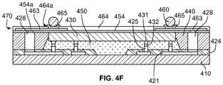
- FIGS. 4A to 4F show cross-sectional views illustrating a method of manufacturing a semiconductor device, in accordance with various aspects of the present disclosure.
- FIG. 5 shows a cross-sectional view illustrating a semiconductor device, in accordance with various aspects of the present disclosure.
- aspects of this disclosure provide a method for manufacturing a semiconductor device and a semiconductor device produced thereby.
- various aspects of this disclosure provide a method for manufacturing a semiconductor device, and a semiconductor device produced thereby, that comprises a transparent, translucent, non-opaque, or otherwise optically-transmissive, external surface.
- “and/or” means any one or more of the items in the list joined by “and/or”.
- “x and/or y” means any element of the three-element set ⁇ (x), (y), (x, y) ⁇ . In other words, “x and/or y” means “one or both of x and y.”
- “x, y, and/or z” means any element of the seven-element set ⁇ (x), (y), (z), (x, y), (x, z), (y, z), (x, y, z) ⁇ . In other words, “x, y and/or z” means “one or more of x, y, and z.”
- first, second, etc. may be used herein to describe various elements, these elements should not be limited by these terms. These terms are only used to distinguish one element from another element. Thus, for example, a first element, a first component or a first section discussed below could be termed a second element, a second component or a second section without departing from the teachings of the present disclosure. Similarly, various spatial terms, such as “upper,” “lower,” “side,” and the like, may be used in distinguishing one element from another element in a relative manner.
- components may be oriented in different manners, for example a semiconductor device may be turned sideways so that its “top” surface is facing horizontally and its “side” surface is facing vertically, without departing from the teachings of the present disclosure.
- the term “on” will be utilized in the document to mean both “on” and “directly on” (e.g., with no intervening layer).
- a semiconductor device comprising a transparent, translucent, non-opaque, or otherwise optically-transmissive, external carrier, wafer, or layer and a manufacturing method thereof.
- optically-transmissive refers to a characteristic of a material that permits passage of light through the material.
- light is used to refer to electromagnetic radiation in the visible light spectrum, i.e., 400-790 terahertz (THz), as well as electromagnetic radiation in the near-infrared light spectrum, i.e., 120-400 THz, and near-ultraviolet light spectrum, i.e., 790-1000 THz.
- the example manufacturing method may, for example, comprise providing a carrier 110 with a first dielectric layer 111 , forming a first conductive layer 121 , forming a second conductive layer 123 and an under bump metal 125 , attaching a first wafer support system (WSS) 1, removing the carrier 110 , forming an opening 111 a in the first dielectric layer 111 , forming a pad or micro bump pad 126 (hereinafter pad 126 ) at the opening 111 a , attaching a semiconductor die 130 and molding with a mold material 140 (e.g., a resin, encapsulant, molding compound, etc.), separating the first WSS 1, attaching an optically-transmissive layer 170 (e.g., a wafer, a panel, a singulated component of a wafer or panel, etc.)
- WSS wafer support system
- a carrier 110 with a first dielectric layer 111 is formed or provided.
- the carrier 110 may provide a planar top surface and a planar bottom surface.
- the carrier 110 (or any carrier discussed herein) may comprise any of a variety of different types of carrier materials.
- the carrier 110 may, for example, comprise a semiconductor material (e.g., silicon, GaAs, etc.), glass, ceramic (e.g., porous ceramic, etc.), metal, etc.
- the carrier 110 may also comprise any of a variety of different types of configurations.
- the carrier 110 may be in a mass form (e.g., a wafer form, a rectangular panel form, etc.).
- the carrier 110 may be in a singular form (e.g., singulated from a wafer or panel, originally formed in a singular form, etc.).
- the carrier 110 may, for example, share any or all characteristics with any carrier discussed herein.
- a first dielectric layer 111 such as, for example, an inorganic dielectric layer (e.g., a silicon oxide layer, a silicon nitride layer, oxide layer, nitride layer, etc.) may be (or may have been) formed on the surface of the carrier 110 .
- the first dielectric layer 111 may have been (or may be) formed through an oxidation process.
- a silicon oxide layer and/or silicon nitride layer of a predetermined thickness may be formed by supplying oxygen gas and/or nitride gas to a silicon wafer at a temperature of approximately 900° C. or higher (e.g., a thermal oxidation process, etc.).
- the first dielectric layer 111 may also comprise a native oxide layer naturally formed on the carrier 110 without manufacturing process assistance.
- the first dielectric layer 111 may also be referred to herein as a protective layer.
- the first dielectric layer 111 may, for example, be from 0.01 to 0.8 microns thick.
- a layer of inorganic material may allow (or assist) a photoetching process to be performed more accurately, so that a conductive layer of a relatively finer line/space/thickness (e.g., trace width, spacing between adjacent traces, and/or trace thickness) may be formed on the layer of inorganic material.
- a conductive layer of a relatively finer line/space/thickness e.g., trace width, spacing between adjacent traces, and/or trace thickness
- a conductive layer with a line/space/thickness of about 2/2/2 micrometers ( ⁇ m) to about 10/10/10 ⁇ m may be formed on a layer of inorganic material (e.g., on a silicon oxide (or silicon dioxide) layer, silicon nitride layer, oxide layer, nitride layer, etc.).
- inorganic material e.g., on a silicon oxide (or silicon dioxide) layer, silicon nitride layer, oxide layer, nitride layer, etc.
- the dielectric layer 111 may comprise an organic material. Additionally, the carrier 110 need not be provided with the dielectric layer 111 .
- a first conductive layer 121 which may also be referred to herein as a redistribution layer, may be formed on the first dielectric layer 111 .
- a first seed layer (not shown) may be formed on the first dielectric layer 111 , and the first conductive layer 121 may be formed on the first seed layer.
- the first conductive layer 121 may then be covered with a second dielectric layer 122 , which may also be referred to herein as a passivation layer.
- the first seed layer and/or any seed layer discussed herein may be formed of any of a variety of materials, including but not limited to tungsten, titanium, equivalents thereof, combinations thereof, alloys thereof, etc.
- the first seed layer may be formed utilizing any of a variety of processes.
- the first seed layer may be formed utilizing one or more of an electroless plating process, an electrolytic plating process, a sputtering process, etc.
- the first seed layer may be formed of TiW with a Cu target.
- the first seed layer and/or any seed layer discussed herein may also be referred to as a conductive layer.
- any seed layer discussed herein may be formed utilizing the same or similar materials and/or processes, or may be formed utilizing different respective materials and/or processes.
- the first seed layer and/or any seed layer discussed herein may comprise multiple layers.
- the first seed layer may comprise a first TiW layer and a second Cu layer.
- the first conductive layer 121 may be formed of any of a variety of materials.
- the first conductive layer 121 may be formed of copper, aluminum, gold, silver, palladium, equivalents thereof, combinations thereof, alloys thereof, other conductive materials, etc.
- the first conductive layer 121 may, for example, be formed utilizing any of a variety of processes.
- the first conductive layer 121 may be formed utilizing one or more of an electroless plating process, an electrolytic plating process, a sputtering process, etc.
- the patterning or routing of the first conductive layer 121 may, for example, be accomplished utilizing any of a variety of processes.
- the first conductive layer 121 may be patterned or routed utilizing a photoetching process using a photoresist, etc.
- photoresist may be spin coated (or otherwise applied, such as a dry film, etc.) on a seed layer.
- the photoresist may then be set using, for example, a masking and illumination process.
- portions of the photoresist may be etched away, residual photoresist may be removed in a descum process, and drying (e.g., spin rinse drying) may be performed to form a template of photoresist.
- the template may be stripped (e.g., chemically stripped, etc.), and the first seed layer that is exposed from the first conductive layer 121 may be etched.
- the first conductive layer 121 and/or any conductive layer discussed herein may also be referred to as a redistribution layer. Also, any conductive layer discussed herein may be formed utilizing the same or similar materials and/or processes, or may be formed utilizing different respective materials and/or processes. Additionally, the first conductive layer 121 , and/or the forming thereof, may share any or all characteristics with any other conductive layer, and/or the forming thereof, disclosed herein.
- the second dielectric layer 122 may be formed of any of a variety of materials.
- the second dielectric layer 122 may be formed of an organic material (e.g., polymers such as polyimide, Benzocyclobutene (BCB), Polybenzoxazole (PBO), equivalents thereof, combinations thereof, etc.).
- the second dielectric layer 122 may be formed of an inorganic material.
- the second dielectric layer 122 may be formed utilizing any of a variety of processes.
- the second dielectric layer 122 may be formed utilizing one or more of spin coating, spray coating, dip coating, rod coating, equivalents thereof, combinations thereof, etc.
- the second dielectric layer 122 and/or any dielectric layer discussed herein may also be referred to as a passivation layer. Also, any dielectric layer discussed herein may be formed utilizing the same or similar materials and/or processes, or may be formed utilizing different respective materials and/or processes. Additionally, the second dielectric layer 121 , and/or the forming thereof, may share any or all characteristics with any other dielectric layer, and/or the forming thereof, disclosed herein.
- the first conductive layer 121 may be formed on the inorganic first dielectric layer 111 (e.g., directly on the inorganic first dielectric layer 111 ), it may be formed or more easily formed to have a finer line/space/thickness in comparison to other conductive layers, which may be formed on organic dielectric layers.
- Formation of the first conductive layer 121 , with or without a seed layer, and the second dielectric layer 122 may be repeated any number of times utilizing the same materials and/or processes or different respective materials and/or processes.
- the example illustrations in FIGS. 1 B- 1 J show two formations of such layers. As such, the layers are provided with similar labels in the figures (e.g., repeating the first conductive layer 121 and the second dielectric layer 122 ).
- An opening or aperture 122 a may be formed in the second dielectric layer 122 , and a specific area of the first conductive layer 121 may be exposed to the outside through the opening 122 a .
- the opening 122 a may be formed in any of a variety of manners (e.g., mechanical and/or laser ablation, chemical etching, photolithography, etc.).
- the second dielectric layer 122 (or any dielectric layer discussed herein) may also be originally formed having opening 122 a , for example by masking, or other selective dielectric layer formation process.
- a second conductive layer 123 and an under bump metal 125 of at least one layer may be formed on the first conductive layer 121 and/or on the second dielectric layer 122 .
- a second seed layer (not shown) may be formed at the inside of the opening 122 a such as, for example, on side walls of the opening 122 a formed in the second dielectric layer 122 and/or on the first conductive layer 121 exposed by the opening 122 a .
- the second seed layer may be formed outside of the opening 122 a such as, for example, on the top surface of the second dielectric layer 122 .
- the second seed layer may be formed using the same materials and/or processes as used to form the first seed layer, or may be formed using different respective materials and/or processes.
- the second seed layer or any seed layer discussed herein may also be referred to herein as a conductive layer.
- the second conductive layer 123 may be formed on the second seed layer.
- the second conductive layer 123 may be formed to fill or at least cover side surfaces of the opening 122 a in the second dielectric layer 122 .
- the second conductive layer 123 may be formed using the same materials and/or processes as the first conductive layer 121 , or may be formed using different respective materials and/or processes.
- the second conductive layer 123 may also be referred to herein as a redistribution layer.
- the second conductive layer 123 may then be covered with the third dielectric layer 124 .
- the third dielectric layer 124 may be formed of any of a variety of materials and/or utilizing any of a variety of dielectric-forming processes.
- the third dielectric layer 124 may be formed utilizing the same materials and/or processes as utilized to form the second dielectric layer 122 .
- An opening or aperture 124 a may be formed in the third dielectric layer 124 , and a specific area of the second conductive layer 123 may be exposed to the outside through the opening 124 a .
- the opening 124 a may be formed in any of a variety of manners such as, for example, mechanical and/or laser ablation, chemical etching, etc.
- the third dielectric layer 124 may be originally formed with the opening 124 a therein.
- An under bump seed layer (not shown) may be formed inside of the opening 124 a such as, for example, on side walls of the opening 124 a formed in the third dielectric layer 124 and/or on the second conductive layer 123 exposed by the opening 124 a .
- the under bump seed layer may be formed outside of the opening 124 a such as, for example, on the top surface of the third dielectric layer 124 around and/or encircling the opening 124 a .
- the under bump seed layer may be formed using the same materials and/or processes as used to form the first seed layer and/or the second seed layer, or may be formed using different respective materials and/or processes.
- the under bump seed layer or any seed layer discussed herein may also be referred to herein as a conductive layer.
- An under bump metal 125 may be formed on the under bump seed layer.
- the under bump metal 125 may be formed of any of a variety of materials, non-limiting examples of which are presented herein.
- the under bump metal 125 may be formed of at least one of chrome, nickel, palladium, gold, silver, alloys thereof, combinations thereof, equivalents thereof, etc.
- the under bump metal 125 may, for example, comprise Ni and Au.
- under bump metal 125 may also, for example, comprise Cu, Ni, and Au.
- the under bump metal 125 may be also formed utilizing any of a variety of processes, non-limiting examples of which are presented herein.
- the under bump metal 125 may be formed utilizing one or more of an electroless plating process, electroplating process, sputtering process, etc.
- the under bump metal 125 may, for example, prevent or inhibit the formation of an intermetallic compound at the interface between the conductive interconnection structure 160 and the second conductive layer 123 , thereby improving the reliability of the connection to the conductive interconnection structure 160 .
- the under bump metal 125 may also be referred to herein as a conductive layer.
- the under bump metal 125 may comprise multiple layers.
- the under bump metal 125 may comprise a first layer of Ni and a second layer of Au.
- an edged trim (or profile) process may be performed, for example in which an edge of the wafer being processed is trimmed (or profiled). Such trimming may be performed in a variety of manners, for example by grinding. Such edge trimming may, for example, protect the wafer from chipping and flaking during subsequent processing.
- the first conductive layer 121 , the second dielectric layer 122 , the second conductive layer 123 , and the third dielectric layer 124 may be considered to be components of an interposer 120 .
- the under bump metal 125 and the pad 126 described herein may also be considered to be components of the interposer 120 .
- the term “interposer” is used herein to refer to a general redistribution structure (e.g., a dielectric and conductor layered structure) that is interposed between other structures, and the scope of this disclosure should not be limited or defined by arbitrary notions regarding interposer composition.
- the first WSS 1 may be attached to the third dielectric layer 124 and the under bump metal 125 .
- the carrier 110 that is shown at the bottom of FIG. 1C is repositioned to the top of FIG. 1D (e.g., the diagram is inverted or rotated).
- the first WSS 1 may be attached to the third dielectric layer 124 and/or to the under bump metal 125 in any of a variety of manners, non-limiting examples of which are provided herein.
- the first WSS 1 (or any WSS discussed herein) may be attached to the third dielectric layer 124 and/or to the under bump metal 125 utilizing a temporary adhesive that loses its adhesion when exposed to thermal energy or light energy, when exposed to particular chemicals, etc.
- One or more additional release layers may also be utilized to ease subsequent release of the first WSS 1.
- the attachment process may, for example, comprise baking the assembly (e.g., at 250° for 30 mins, etc.).
- the first WSS 1 may be formed from any of a variety of materials.
- the first WSS 1 (or any WSS discussed herein) may be formed from one or more of a silicon wafer, a glass wafer, a ceramic wafer, a metal wafer, etc. Though the first WSS 1 is generally presented herein in the form of a wafer, the scope of this disclosure is not limited to such shape.
- the carrier 110 (for example, a silicon wafer on which the first dielectric layer 111 was formed) on a side of the structure opposite the first WSS 1 may be removed.
- most of the carrier 110 may be removed through a mechanical grinding process and then, the remaining carrier 110 may be removed through a chemical etching process.
- a silicon carrier may be ground to 10-30 um thickness, and then the remainder may be removed by a process other than grinding (e.g., by chemical etching, etc.).
- the first WSS 1 comprises a glass wafer or plate
- such glass wafer or plate is removed.
- the first dielectric layer 111 for example, a silicon oxide layer and/or a silicon nitride layer
- the carrier removal process may also remove a portion (or all) of the first dielectric layer 111 ; for example, the first dielectric layer 111 may be thinner after removal of the carrier 110 than when originally formed on the carrier 110 .
- the first dielectric layer 111 may be formed of an inorganic material, and the second and third dielectric layers 122 and 124 may be formed of an organic material.
- the scope of the present disclosure is not limited to such example types of material.
- a plurality of openings 111 a may be selectively formed in the first dielectric layer 111 .
- the openings 111 a may be formed in any of a variety of manners (e.g., mechanical and/or laser ablation, chemical etching, photo etching process, photo-masking and etching process, etc.).
- Each of the openings 111 a may, for example, correspond to a respective specific area of the first conductive layer 121 exposed to the outside by the opening 111 a .
- an opening 111 a exposes a respective specific area of the first conductive layer 121 to the outside through the inorganic first dielectric layer 111 .
- a specific area of the first seed layer, on which the first conductive layer 121 was formed may be exposed to the outside through the inorganic first dielectric layer 111 .
- the dielectric layer may be stripped after such etching, but may also remain in some embodiments as a passivation layer.
- micro bump pads, other pads, lands, attachment structures, or die attachment structures 126 may be formed in the openings 111 a so that each pad 126 is electrically connected to the first conductive layer 121 (e.g., directly connected, connected via a seed layer, etc.).
- a micro bump seed layer (not shown) may be formed inside of the opening 111 a such as, for example, on side walls of the opening 111 a formed in the first dielectric layer 111 and/or on the first conductive layer 121 .
- the micro bump seed layer may be formed outside of the opening 111 a such as, for example, on the top surface of the first dielectric layer 111 surrounding the opening 111 a .
- the micro bump seed layer may be formed utilizing the same materials and/or processes discussed herein with regard to other seed layers or conductive layers, or may be formed utilizing different respective materials and/or processes.
- the micro bump seed layer and/or pad 126 may also be referred to herein as a conductive layer.
- the pad 126 may then be formed on the micro bump seed layer.
- the first seed layer, on which the first conductive layer 121 was formed, and the micro bump seed layer, on which the pad 126 was formed may be interposed between the first conductive layer 121 and the pad 126 .
- the first seed layer and the micro bump seed layer may be directly connected to each other or mutually facing each other.
- the forming of the micro bump seed layer might be skipped, and the pad 126 may be formed on the first seed layer exposed through the opening 111 a.
- the pad 126 may comprise any of a variety of materials, non-limiting examples of which are provided herein.
- the pad 126 may comprise copper, aluminum, gold, silver, palladium, general conductive material, conductive material, equivalents thereof, combinations thereof, alloys thereof, any conductive material discussed herein, etc.
- the pad 126 may comprise Ni and Au.
- the pad 126 may comprise Ni, Au, and Cu.
- the pad 126 may be formed utilizing any of a variety of processes, non-limiting examples of which are provided herein.
- the pad 126 may be formed utilizing one or more of an electroless plating process, an electrolytic plating process, a sputtering process, etc.
- the pad 126 is shown in FIG. 1G extending past (or protruding from) the top surface of the first dielectric layer 111 , but the scope of this disclosure is not limited thereto.
- the pad 126 may comprise a top surface that is coplanar with the top surface of the first dielectric layer 111 , or may comprise a top surface that is below the top surface of the first dielectric layer 111 .
- the pad 126 may comprise any of a variety of geometric configurations, various non-limiting examples of which are provided herein.
- the pad 126 may alternatively be formed in an aperture in the first dielectric layer 111 near the beginning of the overall process shown in FIGS. 1A-1J .
- an aperture may be formed in the first dielectric layer 111 (if such layer exists) and the pad 126 may be formed on the carrier 110 in such aperture before formation of the first conductive layer 121 thereon.
- the semiconductor die 130 may be electrically connected to the pad 126 and may be molded with the mold material 140 .
- the conductive bump 131 (or other conductive attachment structure, for example conductive pillar, etc.) of the semiconductor die 130 is electrically connected to the pad 126 through the solder 132 .
- the term “bump” may collectively refer to a conductive bump or pillar 131 and solder 132 on the pillar 131 .
- the conductive bump 131 of the semiconductor die 130 may be attached to the pad 126 in any of a variety of manners, non-limiting examples of which are presented herein.
- the conductive bump 131 may be soldered to the pad 126 utilizing any of a variety of solder attachment processes (e.g., a mass reflow process, a thermal compression process, a laser soldering process, etc.). Also for example, the conductive bump 131 may be coupled to the pad 126 utilizing a conductive adhesive, paste, etc. Additionally for example, the conductive bump 131 may be coupled to the pad 126 utilizing a direct metal-to-metal (e.g., solderless) bond.
- solder attachment processes e.g., a mass reflow process, a thermal compression process, a laser soldering process, etc.
- the conductive bump 131 may be coupled to the pad 126 utilizing a conductive adhesive, paste, etc.
- the conductive bump 131 may be coupled to the pad 126 utilizing a direct metal-to-metal (e.g., solderless) bond.
- a solder paste may be applied to the pad 126 utilizing a stencil and squeegee, the conductive bump 131 of the semiconductor die 130 may be positioned on or in the solder paste (e.g., utilizing a pick-and-place process), and the solder paste may then be reflowed.
- the assembly may be cleaned (e.g., with hot DI water, etc.), subjected to a flux clean and bake process, subjected to a plasma treatment process, etc.
- an underfill 150 may be formed between the semiconductor die 130 and the first dielectric layer 111 , for example surrounding portions of the conductive bumps 131 and pads 126 that are exposed to (and thus encapsulated by) the underfill 150 .
- the underfill 150 may comprise any of a variety of underfill materials.
- the underfill 150 may be formed utilizing any of a variety of processes (e.g., a capillary underfilling process, utilizing a pre-applied underfill material, etc.).
- the underfill 150 between the semiconductor die 130 and the interposer 120 (as various layers are illustratively grouped in FIG. 1H ) may, for example, prevent or reduce warpage, for example due to thermal expansion coefficient difference between the semiconductor die 130 and the interposer 120 .
- the semiconductor die 130 and/or interposer 120 may be encapsulated with a mold material 140 (e.g., a molding resin or other mold material or encapsulant), which may then be cured.
- the mold material 140 may cover the side surfaces and top surface of the semiconductor die 130 .
- the mold material 140 may only cover the side surfaces of the semiconductor die 130 (or only respective portions thereof), thus leaving the top surface of the semiconductor die 130 exposed from the mold material 140 .
- the mold material 140 may be formed in any of a variety of manners (e.g., compression molding, transfer molding, flood molding, etc.).
- the mold material 140 may comprise any of a variety of types of mold material.
- the mold material 140 may comprise a resin, an epoxy, a thermosetting epoxy molding compound, a room temperature curing type, etc.
- the underfill 150 might not be utilized, and the mold material 140 may instead fill a space or gap between the interposer 120 and the semiconductor die 130 .
- the underfilling process and the molding process may be combined into a single molding process with a molded underfill.
- the semiconductor die 130 may comprise any of a variety of types of semiconductor die, non-limiting examples of which are provided herein.
- the semiconductor die 130 may comprise a digital signal processor (DSP), a microcontroller, a microprocessor, a network processor, a power management processor, an audio processor, a video processor, an RF circuit, a wireless baseband system-on-chip (SoC) processor, a sensor, an application specific integrated circuit, etc.
- DSP digital signal processor
- microcontroller a microcontroller
- a microprocessor a network processor
- a power management processor an audio processor
- a video processor a video processor
- RF circuit a wireless baseband system-on-chip (SoC) processor
- SoC wireless baseband system-on-chip
- a sensor an application specific integrated circuit, etc.
- One or more passive electrical components may also be mounted instead of and/or in addition to the semiconductor die 130 .
- an optically transmissive layer 170 may be attached to the semiconductor die 130 and/or mold material 140 and a second WSS 2 may be attached to the optically transmissive layer 170 .
- the optically transmissive layer 170 may include lenses to direct, guide, or focus light, antireflective layers or coatings that provide light antireflective properties, polarization layers or coatings that provide light polarization properties, color filter layers or coatings that provide color filtering properties, and/or layers of materials with different refractive indices in order to provide an upper or top surface 133 of the semiconductor die 130 with desired optical properties.
- the semiconductor die 130 may comprise optical sensors, optical receivers, optical transmitters, or other optical devices 130 a that transmit, receive, detect, and/or sense light.
- the optically transmissive layer 170 may help guide or may simply permit passage of light to and/or from such optical devices of the semiconductor 130 .
- a second WSS 2 may be attached to the optically-transmissive layer 170 .
- the second WSS 2 may share any or all characteristics with the first WSS 1.
- the second WSS 2 may, for example, be attached in a similar manner as the first WSS 1 (e.g., utilizing a temporary adhesive, vacuum, mechanical attachment mechanism, etc.).
- the first WSS 1 may be separated from the third dielectric layer 124 and/or under bump metal 125 .
- the first WSS 1 may have been attached to the third dielectric layer 124 and/or to the under bump metal 125 utilizing a temporary adhesive that loses it adhesion (or a substantial portion thereof) when exposed to thermal energy, laser (or light) energy, chemical agents, etc.
- the separation of the first WSS 1 from the third dielectric layer 124 and/or under bump metal 125 may, for example, be performed by exposing the temporary adhesive to the energy and/or chemicals that cause the adhesive to loosen.
- the release layer (e.g., between the adhesive and the first WSS 1) may be subjected to laser (or light) irradiation through the glass WSS 1, to effect or assist with the release of the first WSS 1 from the adhesive.
- Other forms of wafer support system attachment/detachment may be utilized (e.g., vacuum attachment, mechanical attachment, etc.).
- Adhesive utilized to attach the first WSS 1 may, for example, be removed with a solvent if necessary.
- the conductive interconnection structure 160 (or a plurality thereof) may be electrically connected to the exposed under bump metal 125 (e.g., exposed after removal of the first WSS 1). At this point, for example while the optically-transmissive layer 2 is attached to the semiconductor die 130 and the mold material 140 , the conductive interconnection structure 160 may be electrically connected to the under bump metal 125 .
- the conductive interconnection structure 160 may comprise any of a variety of characteristics, non-limiting examples of which are presented herein.
- the conductive interconnection structure 160 may be formed of one of a eutectic solder (Sn37Pb), a high lead solder (Sn95Pb), a lead-free solder (SnAg, SnAu, SnCu, SnZn, SnZnBi, SnAgCu, and SnAgBi), combination thereof, equivalents thereof, etc.
- the conductive interconnection structure 160 may, for example, comprise a conductive ball (e.g., a solder ball, a copper-core solder ball, etc.), a conductive bump, a conductive pillar or post (e.g., a copper pillar, a solder-capped copper pillar, a wire, etc.), etc.
- a conductive ball e.g., a solder ball, a copper-core solder ball, etc.
- a conductive bump e.g., a copper pillar, a solder-capped copper pillar, a wire, etc.
- the conductive interconnection structure 160 may, for example, be connected to the under bump metal 125 utilizing any of a variety of reflow and/or plating processes.
- volatile flux may be deposited (e.g., dotted, printed, etc.) on the under bump metal 125
- the conductive interconnection structure 160 may be deposited (e.g., dropped, etc.) on the volatile flux, and then a reflow temperature of about 150° C. to about 250° C. may be provided.
- the volatile flux may, for example, be volatized and completely removed.
- the conductive interconnection structure 160 may be referred to as a conductive bump, a conductive ball, a conductive pillar, a conductive post, a conductive wire, etc., and may, for example, be mounted on a rigid printed circuit board, a flexible printed circuit board, a lead frame, etc.
- the semiconductor die 130 including the interposer 120 may then be electrically connected (e.g., in a flip-chip form or similar to a flip-chip form, etc.) to any of a variety of substrates (e.g., motherboard substrates, packaging substrates, lead frame substrates, etc.).
- the second WSS 2 may be separated from the optically-transmissive layer 170 .
- the top surface 153 of the optically-transmissive layer 170 may be exposed to the outside.
- the top surface 133 of the semiconductor die 130 and the top surface 143 of the mold material 140 may be optically-exposed to the outside through the optically-transmissive layer 170 .
- the optically-transmissive layer 170 may improve optical characteristics of the semiconductor die 130 via lenses, antireflective coatings, polarization coatings, filters, and/or refractive indices of the materials comprising the optically-transmissive layer 170 .
- the interposer 120 (or package or device 100 ) may, for example, be formed in a mass configuration (e.g., in a wafer, panel, strip, matrix, etc.) or as a single unit.
- the interposer 120 , the mold material 140 , and/or the optically-transmissive layer 170 may be singulated or cut (e.g., sawn by a diamond blade or laser beam, snap-separated, pull-separated, etc.).
- the side surfaces of the interposer 120 , the mold material 140 , and/or the optically-transmissive layer 170 may be made coplanar by such a singulation process.
- a plurality of the packages or devices 100 may be placed (e.g., mold side down) on a saw tape, and then sawed. The saw may, for example, cut through the packages or devices 100 and partially through the saw tape. After sawing, the packages or devices 100 may be baked. After singulation, the individual packages or devices 100 may be individually inserted into trays (e.g., utilizing a pick and place process).
- the present disclosure provides a semiconductor device 100 (and manufacturing method thereof) comprising the interposer 120 , for example without a through silicon via.
- a semiconductor device 100 may, for example, be manufactured utilizing general bumping equipment, for example without utilizing complex and expensive through silicon via production processes.
- a conductive layer having a relatively fine line/space/thickness may be formed first on the carrier 110 (for example, a silicon wafer), and then such carrier 110 may be removed.
- the example semiconductor device 201 may comprise an interposer 220 , a semiconductor die 230 , a mold material 240 , an underfill 250 , a conductive interconnection structure 260 , and an optically-transmissive layer 270 .
- the semiconductor device 201 may, for example, share any or all characteristics with any or all other semiconductor devices presented herein (e.g., the example semiconductor device 100 shown in FIGS. 1A-1J , etc.).
- the interposer 220 may for example comprise: a first seed layer 221 a below a first dielectric layer 211 such as, for example, a silicon oxide layer and/or a silicon nitride layer; a first conductive layer 221 below the first seed layer 221 a ; a second dielectric layer 222 covering the first conductive layer 221 or portions thereof; a second seed layer 223 a below the first conductive layer 221 ; a second conductive layer 223 below the second seed layer 223 a ; and a third dielectric layer 224 covering the second conductive layer 223 or portions thereof.
- the line/space/thickness of the first conductive layer 221 may be smaller than those of the second conductive layer 223 .
- the interposer 220 may comprise the micro bump seed layer extending into and/or through the first dielectric layer 211 such as, for example, through an opening 211 a formed therein and on the first seed layer 221 a , a pad or micro bump pad 226 (hereinafter pad 226 ) on the micro bump seed layer 226 a , an under bump seed layer 225 a below the second conductive layer 223 , and an under bump metal 225 below the under bump seed layer 225 a .
- the first seed layer and the micro bump seed layer are directly and electrically connected to each other.
- interposer may be utilized herein to conveniently group various layers for discussion.
- an interposer or interposer structure may comprise any of a variety of the layers discussed herein, and is not limited to any particular set of layers.
- the conductive bump 231 may be on the semiconductor die 230 , and the conductive bump 231 may be electrically connected to the pad 226 through the solder 232 .
- the underfill 250 may be located between the semiconductor die 230 and the interposer 220 such as on the first dielectric layer 211 , and the mold material 240 may surround side surfaces of the semiconductor die 230 and the underfill 250 .
- the top surface 233 of the semiconductor die 230 may be optically-exposed to the outside via the optically-transmissive layer 270 .
- the top surface of the semiconductor die 230 and the top surface 243 of the mold material 240 may be coplanar.
- the conductive interconnection structure 260 may, for example, be connected to the under bump metal 226 and may also be mounted on a substrate as discussed herein.
- Labels (1), (2), and (3) shown in FIG. 2 may, for example, show a lamination and/or formation order.
- the interposer 220 may be formed in the direction (1) that builds from the first dielectric layer 211 .
- the semiconductor die 230 may be connected to the interposer 220 in the direction (2) that builds from the interposer 220 .
- the conductive interconnection structure 260 may then be attached to the interposer 220 in the direction (3) that builds from the interposer 220 .
- the example semiconductor device 200 comprises a pad 226 that is wider at a top end to be connected with a conductive bump 231 of the semiconductor die 230 than at a bottom end extending through the first dielectric layer 211 .
- the pad 226 may be cup-shaped or mushroom-shaped with sloped stem sidewalls or vertical stem sidewalls.
- the pad 226 may also be formed with vertical cap sidewalls.
- FIGS. 3A-3J cross-sectional views illustrating a method of manufacturing a semiconductor device 300 , in accordance with various aspects of the present disclosure is shown.
- the example semiconductor devices and/or methods illustrated in FIGS. 3A-3J may share any or all characteristics with any or all of the other example semiconductor devices and/or methods presented herein.
- the example method of manufacturing the semiconductor device 300 may, for example, comprise providing a carrier 310 , forming an under bump metal 321 , forming a first conductive layer 323 , forming a second conductive layer 325 , forming a pad or micro bump pad 327 (hereinafter pad 327 ) attaching a semiconductor die 330 , molding with a mold material 340 , attaching a optically-transmissive layer 370 (e.g., a wafer, a panel, a singulated component of a wafer or panel, etc.), attaching a first WSS 1, removing the carrier 310 , connecting a conductive interconnection structure 360 , and separating the first WSS 1.
- pad 327 a pad or micro bump pad 327
- a carrier 310 may be provided that comprises a silicon (or semiconductor) wafer with a planar top surface and a planar bottom surface.
- an under bump metal 321 of at least one layer may be directly formed on the carrier 310 .
- the under bump metal 321 may be formed of any of a variety of materials, non-limiting examples of which are presented herein.
- the under bump metal 321 may be formed of at least one of chrome, nickel, palladium, gold, silver, alloys thereof, combinations thereof, equivalents thereof, etc.
- the under bump metal 321 may, for example, comprise Ni and Au.
- the under bump metal 321 may also, for example, comprise Cu, Ni, and Au.
- the under bump metal 321 may be also formed utilizing any of a variety of processes, non-limiting examples of which are presented herein.
- the under bump metal 321 may be formed utilizing one or more of an electroless plating process, electroplating process, sputtering process, etc. on the carrier 310 .
- the under bump metal 321 may, for example, prevent or inhibit the formation of an intermetallic compound at the interface between the conductive interconnection structure 360 and the first conductive layer 323 , thereby improving the reliability of the connection to the conductive interconnection structure 360 .
- the under bump metal 321 may comprise multiple layers on the carrier 310 .
- the under bump metal 321 may comprise a first layer of Ni and a second layer of Au.
- the under bump metal 321 may then be covered with a first dielectric layer 322 such as an organic layer (e.g., polymers such as polyimide, Benzocyclobutene (BCB), Polybenzoxazole (PBO), equivalents thereof, combinations thereof, etc.), which may also be referred to as a passivation layer.
- a first dielectric layer 322 such as an organic layer (e.g., polymers such as polyimide, Benzocyclobutene (BCB), Polybenzoxazole (PBO), equivalents thereof, combinations thereof, etc.), which may also be referred to as a passivation layer.
- the first dielectric layer 322 may be formed on the under bump metal 321 and the top surface of the carrier 310 .
- the first dielectric layer 322 may be formed utilizing one or more of spin coating, spray coating, dip coating, rod coating, equivalents thereof, combinations thereof, etc., but the scope of the present disclosure is not limited thereto.
- the first dielectric layer 322 may
- An opening 322 a may, for example, be formed in the first dielectric layer 322 , and a specific area of the under bump metal 321 (e.g., the entire top surface, a portion of the top surface, a center region of the top surface, etc.) may be exposed to the outside through the opening 322 a .
- the opening 322 a may be formed in any of a variety of manners (e.g., mechanical and/or laser ablation, chemical etching, photolithography, etc.).
- the first dielectric layer 322 (or any dielectric layer discussed herein) may also be originally formed having opening 322 a , for example by masking, or other selective dielectric layer formation process.
- the first conductive layer 323 may be formed on the under bump metal 321 and the first dielectric layer 322 .
- the first conductive layer 323 may be coupled to the under bump metal 321 .
- a first seed layer similar to a seed layer of FIG. 2 , may be formed on the under bump metal 321 and the first dielectric layer 322 .
- the first conductive layer 323 may then be formed on the first seed layer.
- the first conductive layer 323 and/or the forming thereof may, for example, share any or all characteristics with any other conductive layer and/or the forming thereof discussed herein.
- the first conductive layer 323 may then be covered with a second dielectric layer 324 .
- the second dielectric layer 324 may also be referred to as a passivation layer.
- the second dielectric layer 324 and/or the forming thereof may, for example, share any or all characteristics with any other dielectric layer and/or the forming thereof discussed herein.
- An opening or aperture 324 a may, for example, be formed in the second dielectric layer 324 , and a specific area of the first conductive layer 323 may be exposed to the outside through the opening 324 a .
- the opening 324 a and/or the forming thereof may, for example, share any or all characteristics with any other dielectric layer opening and/or the forming thereof discussed herein.
- the line/space/thickness of the first conductive layer 323 may, for example, be formed larger in comparison to the line/space/thickness of the second conductive layer 325 discussed below.
- the scope of this disclosure is not limited to such relative dimensions.
- a second conductive layer 325 may be formed on the first conductive layer 323 and/or on the second dielectric layer 324 .
- a second seed layer similar to a seed layer of FIG. 2 , may be formed on a top surface of the second dielectric layer 324 and/or in an opening or aperture 324 a thereof that extends through the second dielectric layer 324 to the first conductive layer 323 (e.g., on side walls of the opening 324 a ).
- the second seed layer and/or the forming thereof may, for example, share any or all characteristics with any seed layer and/or the forming thereof discussed herein.
- the second conductive layer 325 may then be formed on the second seed layer.
- the second conductive layer 325 and/or the forming thereof may, for example, share any or all characteristics with any conductive layer and/or the forming thereof discussed herein.
- the second conductive layer 325 may then be covered with a third dielectric layer 326 , which may also be referred to as a passivation layer.
- the third dielectric layer 326 and/or the forming thereof may, for example, share any or all characteristics with any dielectric layer and/or the forming thereof discussed herein.
- an opening 326 a may be formed in the third dielectric layer 326 so that a specific area of the second conductive layer 325 corresponding to the opening 326 a is exposed to the outside.
- the opening 326 a and/or the forming thereof may, for example, share any or all characteristics with any other dielectric layer opening and/or the forming thereof discussed herein.
- the forming of the second conductive layer 325 (e.g., with or without a seed layer) and the third dielectric layer 326 may be repeated any number of times (e.g., utilizing the same materials and/or processes or different respective materials and/or processes).
- the example illustrations in FIG. 3E shows two formations of such layers. As such, the layers are provided with similar labels in the figures (e.g., repeating the second conductive layer 325 and the third dielectric layer 326 ).
- a micro bump pads, other pads, landings, attachment structures, or die attachment structures 327 may be formed in openings 326 a so that each pad 327 is electrically connected to the second conductive layer 325 .
- conductive vias 328 may be formed over openings 326 a along the periphery of the device 300 .
- a seed layer similar to a seed layer of FIG.
- the seed layer and/or the forming thereof may share any or all characteristics with any other seed layer (e.g., micro bump seed layer, etc.) and/or the forming thereof discussed herein.
- the conductive vias 328 may then be formed on the seed layer.
- the conductive vias 328 in some embodiments may comprise conductive pillars.
- the conductive vias 328 in some embodiments may be through-mold-vias (TMVs), which may contain or be made of solder, wire, and/or pillars. Furthermore, such pillars may be plated.
- the seed layer may be interposed between the second conductive layer 325 and the conductive via 328 .
- Each pad 327 and/or the forming thereof may share any or all characteristics with any other pad or micro bump pad and/or the forming thereof discussed herein.
- each conductive via 328 and/or the forming thereof may share any or all characteristics with any other conductive via and/or the forming thereof discussed herein.
- the seed layer, pads 327 , and/or conductive vias 328 may also be referred to herein as a conductive layer.
- the under bump metal 321 , the first dielectric layer 322 , the first conductive layer 323 , the second dielectric layer 324 , the second conductive layer 325 , the third dielectric layer 326 , and the pad 327 may be considered to be components of an interposer 320 .
- the semiconductor die 330 may be electrically connected to the pad 327 and may be molded with a mold material 340 .
- the conductive bump 331 (or other conductive attachment structure) of the semiconductor die 330 may be electrically connected to the pad 327 through the solder 332 .
- the conductive bump 331 of the semiconductor die 330 may be attached to the pad 327 in any of a variety of manners, non-limiting examples of which are presented herein.
- the conductive bump 331 may be soldered to the pad 327 utilizing any of a variety of solder attachment processes (e.g., a mass reflow process, a thermal compression process, etc.).
- the conductive bump 331 may be coupled to the pad 327 utilizing a conductive adhesive, paste, etc. Additionally for example, the conductive bump 331 may be coupled to the pad 327 utilizing a direct metal-to-metal (e.g., solderless) bond.
- the conductive bump 331 and/or the forming thereof may, for example, share any or all characteristics with any conductive bump and/or the forming thereof discussed herein.
- an underfill 350 may be formed between the semiconductor die 330 and the interposer 320 (e.g., the third dielectric layer 326 ), for example, surrounding portions of the conductive bumps 331 and pads 327 that are exposed to (and thus encapsulated by) the underfill 350 .
- the underfill 350 and/or the forming thereof may, for example, share any or all characteristics with any underfill and/or the forming thereof discussed herein.
- the semiconductor die 330 and/or interposer 320 may be encapsulated with a mold material 340 (e.g., a molding resin or other mold material or encapsulant), which may then be cured.
- a mold material 340 e.g., a molding resin or other mold material or encapsulant
- the mold material 340 only covers the side surfaces of the vias 328 and the semiconductor die 330 (or only respective portions thereof), thus leaving the top surface of the vias 328 and the semiconductor die 330 exposed from the mold material 340 .
- the mold material 340 covers the side surfaces and the top surface of the semiconductor die 330 .
- the mold material 340 and/or the forming thereof may, for example, share any or all characteristics with any mold material and/or the forming thereof discussed herein.
- an optically transmissive layer 370 may be attached to the semiconductor die 330 and/or mold material 340 and a first WSS 301 may be attached to the optically transmissive layer 370 .
- the optically transmissive 370 may include lenses, antireflective coatings, color filters, polarization layers, and/or layers of materials with different refractive indices in order to provide an upper or top surface 333 of the semiconductor die 330 with desired optical properties.
- the semiconductor die 330 may comprise image sensors, receivers, transmitters, or other devices 330 a that transmit or receive light.
- the optically transmissive layer 370 may help guide light to and/or from such devices of the semiconductor die 330 .
- the first WSS 301 may be attached to the optically-transmissive layer 370 .
- the WSS 301 may be attached to the opticall-transmissive wafter 370 in any of a variety of manners, non-limiting examples of which are provided herein.
- the WSS 301 or any WSS discussed herein may be attached to the optically-transmissive layer 370 utilizing a temporary adhesive that loses its adhesion when exposed to thermal energy or light energy, when exposed to particular chemicals, etc.
- One or more additional release layers may also be utilized to ease subsequent release of the WSS 301 .
- the attachment process may, for example, comprise baking the assembly (e.g., at 250° for 30 mins, etc.).
- the WSS 301 may be formed from any of a variety of materials optically-transmissive materials such as glass. Though the WSS 301 is generally presented herein in the form of a wafer, the scope of this disclosure is not limited to such shape.
- the carrier 310 may be removed from the under bump metal 321 and the first dielectric layer 322 .
- the carrier 310 may be removed through a mechanical grinding process. Any remaining carrier 310 may be removed through a chemical etching process. The removing of the carrier 310 may, for example, share any or all characteristics with any carrier removing discussed herein.
- the under bump metal 321 may be exposed to the outside through the first dielectric layer 322 .
- the bottom surfaces of the under bump metal 321 may be coplanar with the bottom surface of the first dielectric layer 322 .
- the conductive interconnection structure 360 (or a plurality thereof) is connected to the under bump metal 321 .
- the conductive interconnection structure 360 is electrically connected to the first conductive layer 323 via the under bump metal 321 .
- the conductive interconnection structure 360 and/or the forming thereof may, for example, share any or all characteristics with any other interconnection structure and/or the forming thereof discussed herein.
- the WSS 301 may be separated from the optically-transmissive layer 370 .
- the separating of the WSS 301 may, for example, share any or all characteristics with any wafer support system separating discussed herein.
- the top surface 333 of the semiconductor die 330 may be coplanar with the top surface 343 of the mold material 340 . Furthermore, the top surface 333 of the semiconductor die 330 and the top surface 343 of the mold material 340 may be optically-exposed to the outside through the optically-transmissive layer 370 . In this manner, the optically-transmissive layer 370 may improve optical characteristics of the semiconductor die 330 via lenses, antireflective coatings, filters, and/or refractive indices of the materials comprising the optically-transmissive layer 370 .
- the example semiconductor device 300 may be completed by forming the interposer on a carrier in a build-up or stack manner, electrically connecting the semiconductor die to the interposer, molding the semiconductor die with molding material, removing the carrier and forming the conductive interconnection structure on the interposer. Therefore, in the semiconductor device 300 , misalignment between the first conductive layer and the under bump metal is reduced or eliminated. In addition, in the example semiconductor device 300 , the under bump metal is first formed and the conductive layer, dielectric layer, and micro bump are then formed, thereby simplifying overall fabrication process of the semiconductor device 300 .
- FIGS. 4A-4F cross-sectional views illustrating a method of manufacturing a semiconductor device 400 , in accordance with various aspects of the present disclosure, are shown.
- the example semiconductor devices and/or methods illustrated at FIGS. 4A-4F may, for example, share any or all characteristics with any or all of the other example semiconductor devices and/or methods presented herein.
- the example method of manufacturing the semiconductor device 400 may, for example, comprise providing a carrier 410 , forming a first conductive layer 423 on the carrier 410 , forming a pad, micro bump pad, or under bump metal 425 (hereinafter pad 425 ), attaching a semiconductor die 430 , molding with a mold material 440 , forming an under bump metal 465 , and connecting a conductive interconnection structure 460 .
- an optically-transmissive carrier 410 having a planar top surface and a planar bottom surface is provided.
- the carrier 410 in an example embodiment is provided by a glass wafer; however, other optically-transmissive materials such as polymers, oxides, and metals may be used.
- the carrier 410 and the providing or forming thereof, may for example share any or all characteristics with any carrier and discussed herein.
- a first conductive layer 423 may be formed on the carrier 410 .
- the first conductive layer 423 and/or the forming thereof may, for example, share any or all characteristics with any other conductive layer and/or the forming thereof discussed herein.
- a first seed layer similar to a seed layer of FIG. 2 , may be formed on the optically-transmissive carrier 401 , and the first conductive layer 423 may formed on the first seed layer.
- the first conductive layer 423 may then be covered with a first dielectric layer 424 , which may be transparent, translucent, or otherwise optically-transmissive.
- An opening 424 a may be formed in the first dielectric layer 424 so that a specific area of the first conductive layer 423 corresponding to the opening 424 a is exposed to the outside.
- an opening 424 b may be formed in a central portion of the first dielectric layer 424 so that a central area of the carrier 410 is exposed.
- the first conductive layer 423 , the first dielectric layer 424 , and/or openings or apertures 424 a therein, and/or the formation thereof, may share any or all characteristics with the other conductive layers, dielectric layers, and openings, and/or the formation thereof discussed herein.
- the forming of the first conductive layer 423 , with or without a seed layer, and the first dielectric layer 424 may be repeated any number of times utilizing, for example, the same materials and/or processes or different respective materials and/or processes.
- the example illustrations in FIGS. 4B-4F show a single formation of such layers.
- micro bump pads, other pads, landings, attachment structures, or die attachment structures 425 may be formed in the openings 424 a so that each pad 425 is electrically connected to the second conductive layer 423 .
- conductive vias 428 may be formed over openings 426 a along the periphery of the device 400 .
- a seed layer similar to a seed layer of FIG. 2 , may be formed at the inside of the opening 424 a (e.g., on the second conductive layer 423 exposed by the opening 424 a and/or on side walls of the opening 424 a ) and/or outside of the opening 424 a (e.g., on the top surface of the second dielectric layer 424 ).
- the seed layer may be formed utilizing the same material(s) and/or process(es) discussed herein with regard to other seed layers, or may be formed utilizing different respective material(s) and/or process(es).
- the conductive vias 428 may comprise conductive pillars.
- the conductive vias 428 in some embodiments may be through-mold-vias (TMVs), which may contain or be made of solder, wire, and/or pillars. Furthermore, such pillars may be plated.
- the seed layer may be interposed between the second conductive layer 423 and each pad 425 .
- the seed layer may be interposed between the second conductive layer 423 and each conductive via 428 .
- Each pad 425 and/or the forming thereof may share any or all characteristics with any other pad or micro bump pad and/or the forming thereof discussed herein.
- each conductive via 428 and/or the forming thereof may share any or all characteristics with any other conductive via and/or the forming thereof discussed herein.
- the seed layer, pads 425 , and/or conductive vias 428 may also be referred to herein as a conductive layer.
- an edged trim or profile process may be performed, for example in which an edge of the wafer being processed is trimmed or profiled. Such trimming may be performed in a variety of manners, for example by grinding. Such edge trimming may, for example, protect the wafer from chipping and flaking during subsequent processing.
- a semiconductor die 430 may be electrically connected to the pad 425 and may be molded with a mold material 440 .
- the semiconductor die 430 and/or the attaching thereof may share any or all characteristics with other semiconductor dies and/or the attaching thereof discussed herein.
- a solder paste may be applied to each pad 425 utilizing a stencil and squeegee, each conductive bump 431 of the semiconductor die 430 may be positioned on or in the solder paste (e.g., utilizing a pick-and-place process), and the solder paste may then be reflowed.
- the assembly may be cleaned (e.g., with hot DI water, etc.), subjected to a flux clean and bake process, subjected to a plasma treatment process, etc.
- each conductive bump 431 or other conductive attachment structure of the semiconductor die 430 may be electrically connected to a respective pad 425 through the solder 432 .
- Each conductive bump 431 of the semiconductor die 430 may be attached to a respective pad 425 or other pad or landing structure in any of a variety of manners, non-limiting examples of which are presented herein.
- each conductive bump 431 may be soldered to the pad 425 utilizing any of a variety of solder attachment processes (e.g., a mass reflow process, a thermal compression process, etc.), etc.
- the conductive bump 431 may be coupled to the pad 425 utilizing a conductive adhesive, paste, etc.
- each conductive bump 431 may be coupled to a respective pad 425 utilizing a direct metal-to-metal (e.g., solderless) bond.
- an optically-transmissive underfill 450 may be formed between the semiconductor die 430 and the second dielectric layer 424 and/or carrier 410 surrounding portions of the conductive bumps 431 and pads 425 that are exposed to the underfill 450 .
- the underfill 450 may fill the opening 424 b which exposes a lower surface 433 to the carrier 410 .
- the underfill 450 or the formation thereof, may share any or all characteristics with other underfills discussed herein, except that the underfill 450 is optically-transmissive to permit the passage of light between a lower surface 433 of the semiconductor die 430 and the optically-transmissive carrier 410 .
- the underfill 450 may comprise an optically-transmissive silicone material.
- the semiconductor die 430 and/or interposer 420 may be encapsulated with a mold material 440 such as, for example, a molding resin or other mold material or encapsulant, which may then be cured.
- the mold material 440 and/or the forming thereof may share any or all characteristics with other mold materials and/or the forming thereof discussed herein.
- the mold material 440 covers the side surfaces and top surface of the semiconductor die 430 .
- the mold material 440 only covers the side surfaces of the semiconductor die 430 (or only respective portions thereof), thus leaving the top surface of the semiconductor die 430 exposed from the mold material 440 .
- the mold material 440 is optically-transmissive then as discussed herein, the mold material 440 may also be utilized to form a molded underfill, for example instead of the underfill 450 .
- the mold material 440 , the semiconductor die 430 , and the conductive vias 428 may be ground such that a top surface of the mold material 440 is coplanar with the top surface 435 of the semiconductor die 430 and the top surface of the conductive vias 428 as shown.
- the mold material 440 may cover the top surface 435 .
- the mold material 440 and conductive vias 428 may be ground such that a top surface of the mold material 440 is coplanar with the top surface of the conductive vias 428 .
- a top surface of the mold material 440 may not be coplanar with a top surface 435 of the semiconductor die 430 .
- the mold material 440 and semiconductor die 430 may be covered with a passivation layer such as, for example, a third dielectric layer 454 as shown in FIG. 4F , which may provide a planar surface upon which to form further layers of the device 400 .
- a passivation layer such as, for example, a third dielectric layer 454 as shown in FIG. 4F , which may provide a planar surface upon which to form further layers of the device 400 .
- an upper surface of the mold material 440 , semiconductor die 430 , and/or the conductive vias 428 may be covered with a second dielectric layer 454 .
- an opening 454 a may be formed in the second dielectric layer 454 to expose conductive vias 428 .
- a second conductive layer 463 may be formed on the conductive vias 428 and/or on the second dielectric layer 454 .
- a second seed layer (not shown) may be formed at the inside of the opening 454 a such as, for example, on side walls of the opening 454 a formed in the second dielectric layer 454 and/or on the conductive vias 428 exposed by the opening 454 a .
- the second seed layer may be formed outside of the opening 454 a such as, for example, on the top surface of the second dielectric layer 454 .
- the second seed layer may be formed using the same materials and/or processes as used to form the first seed layer, or may be formed using different respective materials and/or processes.
- the second seed layer or any seed layer discussed herein may also be referred to herein as a conductive layer.
- the second conductive layer 463 may be formed on the second seed layer.
- the second conductive layer 463 may be formed to fill or at least cover side surfaces of the opening 454 a in the second dielectric layer 454 .
- the second conductive layer 463 may be formed using the same materials and/or processes as the first conductive layer 421 , or may be formed using different respective materials and/or processes.
- the second conductive layer 463 may also be referred to herein as a redistribution layer.
- the second conductive layer 463 may then be covered with a fourth dielectric layer 464 .
- the fourth dielectric layer 464 and/or the forming thereof may share any or all characteristics with other dielectric layers and/or the forming thereof discussed herein.
- An opening or aperture 464 a may be formed in the fourth dielectric layer 464 , and a specific area of the second conductive layer 463 may be exposed to the outside through the opening 464 a .
- the opening 464 a may be formed in any of a variety of manners such as, for example, mechanical and/or laser ablation, chemical etching, etc.
- the fourth dielectric layer 464 may be originally formed with the opening 464 a therein.
- An under bump seed layer may be formed at the inside of the opening 464 a and/or outside of the opening 464 a .
- the under bump seed layer and/or the forming thereof may share any or all characteristics with any other under bump seed layer and/or the forming thereof discussed herein.
- An under bump metal 465 may be formed on the under bump seed layer.
- the under bump metal 465 and/or the forming thereof may, for example, share any or all characteristics with any under bump metal and/or the forming thereof.
- a conductive interconnection structure 460 may be attached to the under bump metal 465 .
- the conductive interconnection structure 460 and/or the attachment thereof may share any or all characteristics with other conductive interconnection structures and/or the attachment thereof discussed herein.
- the under bump metal 465 may be formed on the opening 464 a of the fourth dielectric layer 464 and the conductive interconnection structure 460 may connected to the under bump metal 465 .
- the second conductive layer 463 may electrically connect the under bump metal 465 to the conductive vias 428 which may likewise be electrically connected to the first conductive layer 421 and/or the second conductive layer 423 .
- the conductive interconnection structure 460 may be electrically connected to semiconductor die 430 via one or more of the conductive layers 421 , 423 , 463 and/or the conductive vias 428 .
- the first conductive layer 421 , the first dielectric layer 422 , the second conductive layer 423 , and the second dielectric layer 424 may be considered to be components of a first interposer 420 .
- the above-mentioned pads 425 also may be considered to be components of the first interposer 420 .
- the under bump metal 465 and fourth dielectric layer 464 may be considered to be components of a second interposer 470 .
- the bottom surface 433 of the semiconductor die 430 may be optically-exposed to the outside through the optically-transmissive underfill 450 , the optically-transmissive carrier 410 , and optically transmissive dielectric layers 422 and 424 .
- the optically-transmissive carrier 410 may improve optical characteristics of the semiconductor die 430 via lenses, antireflective coatings, filters, and/or refractive indices of the materials comprising the optically-transmissive carrier 410 .
- the interposer 420 or package 400 may be formed in a mass configuration or as a single unit. As discussed herein, in an example scenario in which the interposer 420 or package 400 is formed in a mass configuration, a singulation process may be performed.
- the semiconductor device 500 may be constructed in a manner similar to the semiconductor device 400 of FIGS. 4A-4F .
- the semiconductor device 500 includes a plurality of semiconductor dies 530 which are optically isolated from each other via mold material 540 .
- the semiconductor device 500 similar to the semiconductor device 400 , may comprise an interposer 520 , a mold material 540 , an optically-transmissive underfill 550 , a conductive interconnection structure 560 , and an optically-transmissive layer 570 .
- the semiconductor device 500 may, for example, share any or all characteristics with any or all other semiconductor devices presented herein.
- Each semiconductor die 530 may include optical sensors, optical receivers, optical transmitters, or other optical devices that transmit, receive, detect, and/or sense light.
- one semiconductor die 530 a may include one or more optical transmitters 531 configured to transmit or emit light through the optically transmissive underfill 550 and optically transmissive layer 570 .
- pads or micro bump pads 525 may be positioned toward a periphery of the semiconductor die 530 a and outside a transmission region or window 576 of the optically transmissive layer 570 through which the optical transmitter transmits light.
- another semiconductor die 530 b may include one or more optical receivers configured to receive light through the optically transmissive underfill 550 and optically transmissive layer 570 .
- the pads 525 may be positioned toward a periphery of the semiconductor die 530 b and outside a reception region or window 578 of the optically transmissive layer 570 through which the optical transmitter receives light.
- various aspects of this disclosure provide a method for manufacturing a semiconductor device in which the method comprises providing an interposer without through silicon vias and/or an optically-transmissive carrier, wafer, or layer.
- Various aspects of this disclosure also provide a semiconductor device comprising an interposer without through silicon vias and/or an optically-transmissive carrier, wafer, or layer.
Abstract
Description
Claims (20)
Priority Applications (2)
| Application Number | Priority Date | Filing Date | Title |
|---|---|---|---|
| US17/026,752 US11437552B2 (en) | 2016-09-06 | 2020-09-21 | Semiconductor device with transmissive layer and manufacturing method thereof |
| US17/902,035 US11942581B2 (en) | 2016-09-06 | 2022-09-02 | Semiconductor device with transmissive layer and manufacturing method thereof |
Applications Claiming Priority (4)
| Application Number | Priority Date | Filing Date | Title |
|---|---|---|---|
| US15/256,970 US9960328B2 (en) | 2016-09-06 | 2016-09-06 | Semiconductor device and manufacturing method thereof |
| US15/947,245 US10490716B2 (en) | 2016-09-06 | 2018-04-06 | Semiconductor device with optically-transmissive layer and manufacturing method thereof |
| US16/686,516 US10784422B2 (en) | 2016-09-06 | 2019-11-18 | Semiconductor device with optically-transmissive layer and manufacturing method thereof |
| US17/026,752 US11437552B2 (en) | 2016-09-06 | 2020-09-21 | Semiconductor device with transmissive layer and manufacturing method thereof |
Related Parent Applications (1)
| Application Number | Title | Priority Date | Filing Date |
|---|---|---|---|
| US16/686,516 Continuation US10784422B2 (en) | 2016-09-06 | 2019-11-18 | Semiconductor device with optically-transmissive layer and manufacturing method thereof |
Related Child Applications (1)
| Application Number | Title | Priority Date | Filing Date |
|---|---|---|---|
| US17/902,035 Continuation US11942581B2 (en) | 2016-09-06 | 2022-09-02 | Semiconductor device with transmissive layer and manufacturing method thereof |
Publications (2)
| Publication Number | Publication Date |
|---|---|
| US20210020813A1 US20210020813A1 (en) | 2021-01-21 |
| US11437552B2 true US11437552B2 (en) | 2022-09-06 |
Family
ID=59842795
Family Applications (5)
| Application Number | Title | Priority Date | Filing Date |
|---|---|---|---|
| US15/256,970 Active US9960328B2 (en) | 2016-09-06 | 2016-09-06 | Semiconductor device and manufacturing method thereof |
| US15/947,245 Active US10490716B2 (en) | 2016-09-06 | 2018-04-06 | Semiconductor device with optically-transmissive layer and manufacturing method thereof |
| US16/686,516 Active US10784422B2 (en) | 2016-09-06 | 2019-11-18 | Semiconductor device with optically-transmissive layer and manufacturing method thereof |
| US17/026,752 Active 2036-10-27 US11437552B2 (en) | 2016-09-06 | 2020-09-21 | Semiconductor device with transmissive layer and manufacturing method thereof |
| US17/902,035 Active US11942581B2 (en) | 2016-09-06 | 2022-09-02 | Semiconductor device with transmissive layer and manufacturing method thereof |
Family Applications Before (3)
| Application Number | Title | Priority Date | Filing Date |
|---|---|---|---|
| US15/256,970 Active US9960328B2 (en) | 2016-09-06 | 2016-09-06 | Semiconductor device and manufacturing method thereof |
| US15/947,245 Active US10490716B2 (en) | 2016-09-06 | 2018-04-06 | Semiconductor device with optically-transmissive layer and manufacturing method thereof |
| US16/686,516 Active US10784422B2 (en) | 2016-09-06 | 2019-11-18 | Semiconductor device with optically-transmissive layer and manufacturing method thereof |
Family Applications After (1)
| Application Number | Title | Priority Date | Filing Date |
|---|---|---|---|
| US17/902,035 Active US11942581B2 (en) | 2016-09-06 | 2022-09-02 | Semiconductor device with transmissive layer and manufacturing method thereof |
Country Status (4)
| Country | Link |
|---|---|
| US (5) | US9960328B2 (en) |
| KR (1) | KR20180027304A (en) |
| CN (2) | CN107799426A (en) |
| TW (2) | TWI685130B (en) |
Cited By (1)
| Publication number | Priority date | Publication date | Assignee | Title |
|---|---|---|---|---|
| US11942581B2 (en) * | 2016-09-06 | 2024-03-26 | Amkor Technology Singapore Holding Pte. Ltd. | Semiconductor device with transmissive layer and manufacturing method thereof |
Families Citing this family (27)
| Publication number | Priority date | Publication date | Assignee | Title |
|---|---|---|---|---|
| US10884551B2 (en) | 2013-05-16 | 2021-01-05 | Analog Devices, Inc. | Integrated gesture sensor module |
| US10535611B2 (en) * | 2015-11-20 | 2020-01-14 | Apple Inc. | Substrate-less integrated components |
| US10566369B2 (en) * | 2016-12-22 | 2020-02-18 | UTAC Headquarters Pte. Ltd. | Image sensor with processor package |
| KR102317874B1 (en) * | 2017-02-09 | 2021-10-28 | 삼성디스플레이 주식회사 | Display device and manufacturing method of the same |
| US10665765B2 (en) | 2017-02-10 | 2020-05-26 | Advanced Semiconductor Engineering, Inc. | Semiconductor device package and a method of manufacturing the same |
| JP6787413B2 (en) * | 2017-02-17 | 2020-11-18 | 株式会社村田製作所 | Circuit module and manufacturing method of circuit module |
| US10256114B2 (en) | 2017-03-23 | 2019-04-09 | Amkor Technology, Inc. | Semiconductor device with tiered pillar and manufacturing method thereof |
| US10103038B1 (en) * | 2017-08-24 | 2018-10-16 | Micron Technology, Inc. | Thrumold post package with reverse build up hybrid additive structure |
| US20190067248A1 (en) | 2017-08-24 | 2019-02-28 | Micron Technology, Inc. | Semiconductor device having laterally offset stacked semiconductor dies |
| US10304697B2 (en) * | 2017-10-05 | 2019-05-28 | Amkor Technology, Inc. | Electronic device with top side pin array and manufacturing method thereof |
| KR101994758B1 (en) * | 2017-10-16 | 2019-07-01 | 삼성전기주식회사 | Thin type inductor |
| US10712197B2 (en) * | 2018-01-11 | 2020-07-14 | Analog Devices Global Unlimited Company | Optical sensor package |
| US10700008B2 (en) * | 2018-05-30 | 2020-06-30 | Taiwan Semiconductor Manufacturing Co., Ltd. | Package structure having redistribution layer structures |
| CN109037181A (en) * | 2018-07-23 | 2018-12-18 | 华进半导体封装先导技术研发中心有限公司 | A kind of fan-out packaging structure and its manufacturing method improving warpage |
| DE102018119538A1 (en) * | 2018-08-10 | 2020-02-13 | Osram Opto Semiconductors Gmbh | OPTOELECTRONIC SEMICONDUCTOR COMPONENT AND PRODUCTION METHOD FOR OPTOELECTRONIC SEMICONDUCTOR COMPONENTS |
| KR20200030411A (en) * | 2018-09-12 | 2020-03-20 | 엘지이노텍 주식회사 | Flexible circuit board and chip pakage comprising the same, and electronic device comprising the same |
| KR102564324B1 (en) | 2018-10-15 | 2023-08-07 | 삼성전자주식회사 | Apparatus of semiconductor memory and method of manufacturing the same |
| KR102513085B1 (en) * | 2018-11-20 | 2023-03-23 | 삼성전자주식회사 | Fan-out semiconductor package |
| WO2020153331A1 (en) * | 2019-01-24 | 2020-07-30 | 株式会社村田製作所 | Module |
| US11211515B2 (en) * | 2019-02-27 | 2021-12-28 | Apple Inc. | Edge-mountable semiconductor chip package |
| EP3738922A1 (en) * | 2019-05-13 | 2020-11-18 | AT & S Austria Technologie & Systemtechnik Aktiengesellschaft | Hermetic optical component package having organic portion and inorganic portion |
| US11019721B2 (en) * | 2019-09-05 | 2021-05-25 | Hannstouch Solution Incorporated | Manufacturing method of flexible electronic device |
| US11282772B2 (en) * | 2019-11-06 | 2022-03-22 | Advanced Semiconductor Engineering, Inc. | Package structure, assembly structure and method for manufacturing the same |
| TWI758167B (en) * | 2021-04-21 | 2022-03-11 | 欣興電子股份有限公司 | Package structure and manufacturing method thereof |
| US11682612B2 (en) | 2021-04-21 | 2023-06-20 | Unimicron Technology Corp. | Package structure and manufacturing method thereof |
| US11908757B2 (en) * | 2021-06-18 | 2024-02-20 | Taiwan Semiconductor Manufacturing Company Limited | Die corner removal for molding compound crack suppression in semiconductor die packaging and methods for forming the same |
| CN113910515A (en) * | 2021-10-29 | 2022-01-11 | 西安微电子技术研究所 | Device and method for reinforcing radiating gasket inside power module |
Citations (359)
| Publication number | Priority date | Publication date | Assignee | Title |
|---|---|---|---|---|
| US3462349A (en) | 1966-09-19 | 1969-08-19 | Hughes Aircraft Co | Method of forming metal contacts on electrical components |
| US3868724A (en) | 1973-11-21 | 1975-02-25 | Fairchild Camera Instr Co | Multi-layer connecting structures for packaging semiconductor devices mounted on a flexible carrier |
| US3916434A (en) | 1972-11-30 | 1975-10-28 | Power Hybrids Inc | Hermetically sealed encapsulation of semiconductor devices |
| US4322778A (en) | 1980-01-25 | 1982-03-30 | International Business Machines Corp. | High performance semiconductor package assembly |
| US4532419A (en) | 1982-09-09 | 1985-07-30 | Sony Corporation | Memory card having static electricity protection |
| US4642160A (en) | 1985-08-12 | 1987-02-10 | Interconnect Technology Inc. | Multilayer circuit board manufacturing |
| US4645552A (en) | 1984-11-19 | 1987-02-24 | Hughes Aircraft Company | Process for fabricating dimensionally stable interconnect boards |
| US4685033A (en) | 1984-08-28 | 1987-08-04 | Nec Corporation | Multilayer wiring substrate |
| US4706167A (en) | 1983-11-10 | 1987-11-10 | Telemark Co., Inc. | Circuit wiring disposed on solder mask coating |
| US4716049A (en) | 1985-12-20 | 1987-12-29 | Hughes Aircraft Company | Compressive pedestal for microminiature connections |
| US4786952A (en) | 1986-07-24 | 1988-11-22 | General Motors Corporation | High voltage depletion mode MOS power field effect transistor |
| US4806188A (en) | 1988-03-04 | 1989-02-21 | E. I. Du Pont De Nemours And Company | Method for fabricating multilayer circuits |
| US4811082A (en) | 1986-11-12 | 1989-03-07 | International Business Machines Corporation | High performance integrated circuit packaging structure |
| US4897338A (en) | 1987-08-03 | 1990-01-30 | Allied-Signal Inc. | Method for the manufacture of multilayer printed circuit boards |
| US4905124A (en) | 1987-03-31 | 1990-02-27 | Mitsubishi Denki Kabushiki Kaisha | IC card |
| US4964212A (en) | 1988-09-29 | 1990-10-23 | Commissariat A L'energie Atomique | Process for producing electrical connections through a substrate |
| US4974120A (en) | 1989-01-12 | 1990-11-27 | Mitsubishi Denki Kabushiki Kaisha | IC card |
| US4996391A (en) | 1988-09-30 | 1991-02-26 | Siemens Aktiengesellschaft | Printed circuit board having an injection molded substrate |
| US5021047A (en) | 1989-08-29 | 1991-06-04 | Movern John B | Restricted use hypodermic syringe |
| US5072075A (en) | 1989-06-28 | 1991-12-10 | Digital Equipment Corporation | Double-sided hybrid high density circuit board and method of making same |
| US5072520A (en) | 1990-10-23 | 1991-12-17 | Rogers Corporation | Method of manufacturing an interconnect device having coplanar contact bumps |
| US5081520A (en) | 1989-05-16 | 1992-01-14 | Minolta Camera Kabushiki Kaisha | Chip mounting substrate having an integral molded projection and conductive pattern |
| US5091769A (en) | 1991-03-27 | 1992-02-25 | Eichelberger Charles W | Configuration for testing and burn-in of integrated circuit chips |
| US5108553A (en) | 1989-04-04 | 1992-04-28 | Olin Corporation | G-tab manufacturing process and the product produced thereby |
| US5110664A (en) | 1989-07-10 | 1992-05-05 | Hitachi, Ltd. | Thick film and thin film composite substrate and electronic circuit apparatus using it |
| US5191174A (en) | 1990-08-01 | 1993-03-02 | International Business Machines Corporation | High density circuit board and method of making same |
| JPH05109975A (en) | 1991-10-14 | 1993-04-30 | Hitachi Ltd | Resin-sealed type semiconductor device |
| JPH05136323A (en) | 1991-11-13 | 1993-06-01 | Nec Corp | Integrated circuit device |
| US5229550A (en) | 1990-10-30 | 1993-07-20 | International Business Machines Corporation | Encapsulated circuitized power core alignment and lamination |
| US5239448A (en) | 1991-10-28 | 1993-08-24 | International Business Machines Corporation | Formulation of multichip modules |
| US5247429A (en) | 1990-11-21 | 1993-09-21 | Nippondenso Co., Ltd. | Display board |
| US5250843A (en) | 1991-03-27 | 1993-10-05 | Integrated System Assemblies Corp. | Multichip integrated circuit modules |
| US5278726A (en) | 1992-01-22 | 1994-01-11 | Motorola, Inc. | Method and apparatus for partially overmolded integrated circuit package |
| US5283459A (en) | 1989-11-15 | 1994-02-01 | Kabushiki Kaisha Toshiba | Semiconductor sensor including an aperture having a funnel shaped section intersecting a second section |
| US5353498A (en) | 1993-02-08 | 1994-10-11 | General Electric Company | Method for fabricating an integrated circuit module |
| US5371654A (en) | 1992-10-19 | 1994-12-06 | International Business Machines Corporation | Three dimensional high performance interconnection package |
| US5379191A (en) | 1991-02-26 | 1995-01-03 | Microelectronics And Computer Technology Corporation | Compact adapter package providing peripheral to area translation for an integrated circuit chip |
| JPH0717175A (en) | 1993-06-22 | 1995-01-20 | Seiko Epson Corp | Memory card |
| US5404044A (en) | 1992-09-29 | 1995-04-04 | International Business Machines Corporation | Parallel process interposer (PPI) |
| US5463253A (en) | 1990-03-15 | 1995-10-31 | Fujitsu Limited | Semiconductor device having a plurality of chips |
| US5474958A (en) | 1993-05-04 | 1995-12-12 | Motorola, Inc. | Method for making semiconductor device having no die supporting surface |
| US5474957A (en) | 1994-05-09 | 1995-12-12 | Nec Corporation | Process of mounting tape automated bonded semiconductor chip on printed circuit board through bumps |
| US5508938A (en) | 1992-08-13 | 1996-04-16 | Fujitsu Limited | Special interconnect layer employing offset trace layout for advanced multi-chip module packages |
| US5530288A (en) | 1994-10-12 | 1996-06-25 | International Business Machines Corporation | Passive interposer including at least one passive electronic component |
| US5531020A (en) | 1989-11-14 | 1996-07-02 | Poly Flex Circuits, Inc. | Method of making subsurface electronic circuits |
| JPH08190615A (en) | 1995-01-09 | 1996-07-23 | Seiko Epson Corp | Memory card |
| US5546654A (en) | 1994-08-29 | 1996-08-20 | General Electric Company | Vacuum fixture and method for fabricating electronic assemblies |
| US5574309A (en) | 1991-11-25 | 1996-11-12 | Gemplus Card International | Integrated circuit card comprising means for the protection of the integrated circuit |
| US5581498A (en) | 1993-08-13 | 1996-12-03 | Irvine Sensors Corporation | Stack of IC chips in lieu of single IC chip |
| US5582858A (en) | 1991-10-07 | 1996-12-10 | International Business Machines Corporation | Adhesive layer in multi-level packaging and organic material as a metal diffusion barrier |
| US5616422A (en) | 1994-02-28 | 1997-04-01 | International Business Machines Corporation | Metallized substrate |
| US5637832A (en) | 1993-10-26 | 1997-06-10 | Pacific Microelectronics Corporation | Solder ball array and method of preparation |
| US5674785A (en) | 1995-11-27 | 1997-10-07 | Micron Technology, Inc. | Method of producing a single piece package for semiconductor die |
| US5715292A (en) | 1994-11-25 | 1998-02-03 | Loral Fairchild Corporation | Digital sensor cassette for mammography |
| US5719749A (en) | 1994-09-26 | 1998-02-17 | Sheldahl, Inc. | Printed circuit assembly with fine pitch flexible printed circuit overlay mounted to printed circuit board |
| US5726493A (en) | 1994-06-13 | 1998-03-10 | Fujitsu Limited | Semiconductor device and semiconductor device unit having ball-grid-array type package structure |
| US5739581A (en) | 1995-11-17 | 1998-04-14 | National Semiconductor Corporation | High density integrated circuit package assembly with a heatsink between stacked dies |
| US5739588A (en) | 1994-08-15 | 1998-04-14 | Citizen Watch Co., Ltd. | Semiconductor device |
| US5742479A (en) | 1994-03-09 | 1998-04-21 | Seiko Epson Corporation | Card-type electronic device with plastic frame sandwiched between printed circuit board and metal panel |
| US5774340A (en) | 1996-08-28 | 1998-06-30 | International Business Machines Corporation | Planar redistribution structure and printed wiring device |
| US5798014A (en) | 1995-02-02 | 1998-08-25 | Hestia Technologies, Inc. | Methods of making multi-tier laminate substrates for electronic device packaging |
| US5822190A (en) | 1996-06-11 | 1998-10-13 | Kabushiki Kaisha Toshiba | Card type memory device and a method for manufacturing the same |
| US5826330A (en) | 1995-12-28 | 1998-10-27 | Hitachi Aic Inc. | Method of manufacturing multilayer printed wiring board |
| US5835355A (en) | 1997-09-22 | 1998-11-10 | Lsi Logic Corporation | Tape ball grid array package with perforated metal stiffener |
| US5841193A (en) | 1996-05-20 | 1998-11-24 | Epic Technologies, Inc. | Single chip modules, repairable multichip modules, and methods of fabrication thereof |
| US5847453A (en) | 1996-03-27 | 1998-12-08 | Honda Giken Kogyo Kabushiki Kaisha | Microwave circuit package |
| JPH10334205A (en) | 1997-05-30 | 1998-12-18 | Toshiba Corp | Ic card and memory package |
| US5883425A (en) | 1995-10-27 | 1999-03-16 | Mitsubishi Denki Kabushiki Kaisha | Circuit device |
| US5894108A (en) | 1997-02-11 | 1999-04-13 | National Semiconductor Corporation | Plastic package with exposed die |
| US5903052A (en) | 1998-05-12 | 1999-05-11 | Industrial Technology Research Institute | Structure for semiconductor package for improving the efficiency of spreading heat |
| US5907477A (en) | 1995-09-19 | 1999-05-25 | Micron Communications, Inc. | Substrate assembly including a compartmental dam for use in the manufacturing of an enclosed electrical circuit using an encapsulant |
| US5936843A (en) | 1997-10-14 | 1999-08-10 | Fujitsu Limited | Printed wiring board with mounted circuit element using a terminal density conversion board |
| US5952611A (en) | 1997-12-19 | 1999-09-14 | Texas Instruments Incorporated | Flexible pin location integrated circuit package |
| US6004619A (en) | 1996-11-07 | 1999-12-21 | Hewlett-Packard Company | Process for manufacturing printed circuit boards |
| US6013948A (en) | 1995-11-27 | 2000-01-11 | Micron Technology, Inc. | Stackable chip scale semiconductor package with mating contacts on opposed surfaces |
| US6021564A (en) | 1996-11-08 | 2000-02-08 | W. L. Gore & Associates, Inc. | Method for reducing via inductance in an electronic assembly and article |
| US6028364A (en) | 1994-09-20 | 2000-02-22 | Hitachi, Ltd. | Semiconductor device having a stress relieving mechanism |
| US6034427A (en) | 1998-01-28 | 2000-03-07 | Prolinx Labs Corporation | Ball grid array structure and method for packaging an integrated circuit chip |
| US6035527A (en) | 1996-05-18 | 2000-03-14 | Ingenieurbuero Tamm Factory Innovations | Method for the production of printed circuit boards |
| US6040622A (en) | 1998-06-11 | 2000-03-21 | Sandisk Corporation | Semiconductor package using terminals formed on a conductive layer of a circuit board |
| US6051888A (en) | 1997-04-07 | 2000-04-18 | Texas Instruments Incorporated | Semiconductor package and method for increased thermal dissipation of flip-chip semiconductor package |
| US6060778A (en) | 1997-05-17 | 2000-05-09 | Hyundai Electronics Industries Co. Ltd. | Ball grid array package |
| US6069407A (en) | 1998-11-18 | 2000-05-30 | Vlsi Technology, Inc. | BGA package using PCB and tape in a die-up configuration |
| US6072243A (en) | 1996-11-26 | 2000-06-06 | Sharp Kabushiki Kaisha | Semiconductor integrated circuit device capable of surely electrically insulating two semiconductor chips from each other and fabricating method thereof |
| US6081036A (en) | 1996-04-19 | 2000-06-27 | Matsushita Electronics Corp. | Semiconductor device |
| US6119338A (en) | 1998-03-19 | 2000-09-19 | Industrial Technology Research Institute | Method for manufacturing high-density multilayer printed circuit boards |
| US6122171A (en) | 1999-07-30 | 2000-09-19 | Micron Technology, Inc. | Heat sink chip package and method of making |
| US6127833A (en) | 1999-01-04 | 2000-10-03 | Taiwan Semiconductor Manufacturing Co. | Test carrier for attaching a semiconductor device |
| US6137062A (en) | 1998-05-11 | 2000-10-24 | Motorola, Inc. | Ball grid array with recessed solder balls |
| US6157080A (en) | 1997-11-06 | 2000-12-05 | Sharp Kabushiki Kaisha | Semiconductor device using a chip scale package |
| US6160705A (en) | 1997-05-09 | 2000-12-12 | Texas Instruments Incorporated | Ball grid array package and method using enhanced power and ground distribution circuitry |
| US6172419B1 (en) | 1998-02-24 | 2001-01-09 | Micron Technology, Inc. | Low profile ball grid array package |
| US6175087B1 (en) | 1998-12-02 | 2001-01-16 | International Business Machines Corporation | Composite laminate circuit structure and method of forming the same |
| US6184463B1 (en) | 1998-04-13 | 2001-02-06 | Harris Corporation | Integrated circuit package for flip chip |
| US6194250B1 (en) | 1998-09-14 | 2001-02-27 | Motorola, Inc. | Low-profile microelectronic package |
| US6204453B1 (en) | 1998-12-02 | 2001-03-20 | International Business Machines Corporation | Two signal one power plane circuit board |
| US6214641B1 (en) | 1996-06-25 | 2001-04-10 | Micron Technology, Inc. | Method of fabricating a multi-chip module |
| JP2001118947A (en) | 1999-10-19 | 2001-04-27 | Nec Corp | Semiconductor device and method of manufacturing package therefor |
| US6239485B1 (en) | 1998-11-13 | 2001-05-29 | Fujitsu Limited | Reduced cross-talk noise high density signal interposer with power and ground wrap |
| USD445096S1 (en) | 1998-04-01 | 2001-07-17 | Sandisk Corporation | Removable memory card for use with portable electronic devices |
| US6274821B1 (en) | 1998-09-16 | 2001-08-14 | Denso Corporation | Shock-resistive printed circuit board and electronic device including the same |
| USD446525S1 (en) | 1999-08-24 | 2001-08-14 | Kabushiki Kaisha Toshiba | IC memory card |
| US6280641B1 (en) | 1998-06-02 | 2001-08-28 | Mitsubishi Gas Chemical Company, Inc. | Printed wiring board having highly reliably via hole and process for forming via hole |
| US6294408B1 (en) | 1999-01-06 | 2001-09-25 | International Business Machines Corporation | Method for controlling thermal interface gap distance |
| US6307161B1 (en) | 1996-09-10 | 2001-10-23 | Formfactor, Inc. | Partially-overcoated elongate contact structures |
| US6316285B1 (en) | 1998-09-02 | 2001-11-13 | Micron Technology, Inc. | Passivation layer for packaged integrated circuits |
| US6329609B1 (en) | 2000-06-29 | 2001-12-11 | International Business Machines Corporation | Method and structure to prevent distortion and expansion of organic spacer layer for thin film transfer-join technology |
| US20020011657A1 (en) | 2000-05-19 | 2002-01-31 | Takashi Saito | Semiconductor device, an interposer for the semiconductor device, and a method of manufacturing the same |
| US20020017712A1 (en) | 1998-06-04 | 2002-02-14 | Yoshihiro Bessho | Method for fabricating a semiconductor package with a semiconductor device attached to a multilayered substrate |
| US6351031B1 (en) | 1999-10-12 | 2002-02-26 | Fujitsu Limited | Semiconductor device and method for manufacturing substrate of the same |
| US6353999B1 (en) | 1999-03-09 | 2002-03-12 | Unimicron Taiwan Corp. | Method of making mechanical-laser structure |
| US6365975B1 (en) | 1997-04-02 | 2002-04-02 | Tessera, Inc. | Chip with internal signal routing in external element |
| US6376906B1 (en) | 1997-02-12 | 2002-04-23 | Denso Corporation | Mounting structure of semiconductor element |
| US6392160B1 (en) | 1998-11-25 | 2002-05-21 | Lucent Technologies Inc. | Backplane for radio frequency signals |
| US20020061642A1 (en) | 1999-09-02 | 2002-05-23 | Matsushita Electric Industrial Co., Ltd. | Semiconductor device and method of manufacturing the same |
| US6395578B1 (en) | 1999-05-20 | 2002-05-28 | Amkor Technology, Inc. | Semiconductor package and method for fabricating the same |
| US20020066952A1 (en) | 2000-12-04 | 2002-06-06 | Fujitsu Limited | Semiconductor device having an interconnecting post formed on an interposer within a sealing resin |
| US6407930B1 (en) | 1999-06-23 | 2002-06-18 | Asustek Computer Inc. | Structure of printed circuit board with stacked daughter board |
| US6405431B1 (en) | 1996-06-27 | 2002-06-18 | Samsung Electro-Mechanics Co., Ltd. | Method for manufacturing build-up multi-layer printed circuit board by using yag laser |
| US6406942B2 (en) | 2000-03-09 | 2002-06-18 | Nec Corporation | Flip chip type semiconductor device and method for manufacturing the same |
| US6407341B1 (en) | 2000-04-25 | 2002-06-18 | International Business Machines Corporation | Conductive substructures of a multilayered laminate |
| US6448510B1 (en) | 1997-05-20 | 2002-09-10 | Micro Components Ltd. | Substrate for electronic packaging, pin jig fixture |
| US20020135057A1 (en) | 2001-03-26 | 2002-09-26 | Yoichiro Kurita | Thin planar semiconductor device having electrodes on both surfaces and method of fabricating same |
| US6479762B2 (en) | 2000-11-20 | 2002-11-12 | Alps Electric Co., Ltd. | Printed circuit board having a pattern of traces formed by screen-printing |
| US6486554B2 (en) | 2001-03-30 | 2002-11-26 | International Business Machines Corporation | Molded body for PBGA and chip-scale packages |
| US6486005B1 (en) | 2000-04-03 | 2002-11-26 | Hynix Semiconductor Inc. | Semiconductor package and method for fabricating the same |
| US6497943B1 (en) | 2000-02-14 | 2002-12-24 | International Business Machines Corporation | Surface metal balancing to reduce chip carrier flexing |
| US20020195697A1 (en) | 2001-06-21 | 2002-12-26 | Mess Leonard E. | Stacked mass storage flash memory package |
| US20030025199A1 (en) | 2001-08-01 | 2003-02-06 | Chi-Chuan Wu | Super low profile package with stacked dies |
| US6517995B1 (en) | 1999-09-14 | 2003-02-11 | Massachusetts Institute Of Technology | Fabrication of finely featured devices by liquid embossing |
| US6534391B1 (en) | 2001-08-17 | 2003-03-18 | Amkor Technology, Inc. | Semiconductor package having substrate with laser-formed aperture through solder mask layer |
| US6544638B2 (en) | 1996-11-08 | 2003-04-08 | Gore Enterprise Holdings, Inc. | Electronic chip package |
| US6573598B2 (en) | 1999-04-06 | 2003-06-03 | Oki Electric Industry Co, Ltd. | Semiconductor device and method of fabricating the same |
| US20030102546A1 (en) | 2001-04-17 | 2003-06-05 | Lee Teck Kheng | Method and apparatus for package reduction in stacked chip and board assemblies |
| US6577013B1 (en) | 2000-09-05 | 2003-06-10 | Amkor Technology, Inc. | Chip size semiconductor packages with stacked dies |
| US6586682B2 (en) | 2000-02-23 | 2003-07-01 | Kulicke & Soffa Holdings, Inc. | Printed wiring board with controlled line impedance |
| US20030128096A1 (en) | 2002-01-10 | 2003-07-10 | Joseph Mazzochette | Temperature compensating device with integral sheet thermistors |
| US20030141582A1 (en) | 2002-01-25 | 2003-07-31 | Yang Chaur-Chin | Stack type flip-chip package |
| US6608382B2 (en) | 2001-02-15 | 2003-08-19 | Au Optronics Corporation | Metal bump |
| US6608757B1 (en) | 2002-03-18 | 2003-08-19 | International Business Machines Corporation | Method for making a printed wiring board |
| US20030164540A1 (en) | 2002-03-04 | 2003-09-04 | Lee Teck Kheng | Semiconductor die packages with recessed interconnecting structures and methods for assembling the same |
| US20030197284A1 (en) | 2002-02-21 | 2003-10-23 | United Test & Assembly Center Limited | Semiconductor package |
| US6660559B1 (en) | 2001-06-25 | 2003-12-09 | Amkor Technology, Inc. | Method of making a chip carrier package using laser ablation |
| US20040036183A1 (en) | 2001-11-03 | 2004-02-26 | Samsung Electronics Co., Ltd. | Semiconductor package having DAM and method for fabricating the same |
| US20040063246A1 (en) | 2002-09-17 | 2004-04-01 | Chippac, Inc. | Semiconductor multi-package module having package stacked over die-down flip chip ball grid array package and having wire bond interconnect between stacked packages |
| US6715204B1 (en) | 1998-07-08 | 2004-04-06 | Ibiden Co., Ltd. | Printed wiring board and method for producing the same |
| US6727645B2 (en) | 2002-05-24 | 2004-04-27 | International Business Machines Corporation | Organic LED device |
| US6727576B2 (en) | 2001-10-31 | 2004-04-27 | Infineon Technologies Ag | Transfer wafer level packaging |
| US6730857B2 (en) | 2001-03-13 | 2004-05-04 | International Business Machines Corporation | Structure having laser ablated features and method of fabricating |
| US6734542B2 (en) | 2000-12-27 | 2004-05-11 | Matsushita Electric Industrial Co., Ltd. | Component built-in module and method for producing the same |
| US6740964B2 (en) | 2000-11-17 | 2004-05-25 | Oki Electric Industry Co., Ltd. | Semiconductor package for three-dimensional mounting, fabrication method thereof, and semiconductor device |
| US6753612B2 (en) | 2001-04-05 | 2004-06-22 | International Business Machines Corporation | Economical high density chip carrier |
| US6765287B1 (en) | 2001-07-27 | 2004-07-20 | Charles W. C. Lin | Three-dimensional stacked semiconductor package |
| US20040145044A1 (en) | 2002-01-23 | 2004-07-29 | Matsushita Electric Industrial Co., Ltd. | Circuit component built-in module with embedded semiconductor chip and method of manufacturing |
| US6774748B1 (en) | 1999-11-15 | 2004-08-10 | Nec Corporation | RF package with multi-layer substrate having coplanar feed through and connection interface |
| US20040159462A1 (en) | 1999-06-01 | 2004-08-19 | Chung Kevin Kwong-Tai | Flexible dielectric electronic substrate and method for making same |
| US20040165362A1 (en) | 2003-02-20 | 2004-08-26 | Farnworth Warren M. | Chip scale package structures and method of forming conductive bumps thereon |
| US6787443B1 (en) | 2003-05-20 | 2004-09-07 | Intel Corporation | PCB design and method for providing vented blind vias |
| US6803528B1 (en) | 1999-11-05 | 2004-10-12 | 3M Innovative Properties Company | Multi-layer double-sided wiring board and method of fabricating the same |
| US6815709B2 (en) | 2001-05-23 | 2004-11-09 | International Business Machines Corporation | Structure having flush circuitry features and method of making |
| US6815739B2 (en) | 2001-05-18 | 2004-11-09 | Corporation For National Research Initiatives | Radio frequency microelectromechanical systems (MEMS) devices on low-temperature co-fired ceramic (LTCC) substrates |
| US20040238402A1 (en) | 2003-05-30 | 2004-12-02 | Texas Instruments Incorporated | Method and system for flip chip packaging |
| US20040262774A1 (en) | 2003-06-27 | 2004-12-30 | In-Ku Kang | Multi-chip packages having a plurality of flip chips and methods of manufacturing the same |
| US6838776B2 (en) | 2003-04-18 | 2005-01-04 | Freescale Semiconductor, Inc. | Circuit device with at least partial packaging and method for forming |
| US6845554B2 (en) | 2001-11-22 | 2005-01-25 | Infineon Technologies Ag | Method for connection of circuit units |
| US20050056928A1 (en) | 2001-10-05 | 2005-03-17 | Samsung Electronics Co., Ltd. | Semiconductor package |
| US20050062154A1 (en) | 2003-09-18 | 2005-03-24 | International Business Machines Corporation | Electronically grounded heat spreader |
| US20050073605A1 (en) | 2003-10-06 | 2005-04-07 | Burns Jeffrey H. | Integrated optical filter |
| US6888240B2 (en) | 2001-04-30 | 2005-05-03 | Intel Corporation | High performance, low cost microelectronic circuit package with interposer |
| US6905914B1 (en) | 2002-11-08 | 2005-06-14 | Amkor Technology, Inc. | Wafer level package and fabrication method |
| US20050133932A1 (en) | 2003-12-19 | 2005-06-23 | Jens Pohl | Semiconductor module with a semiconductor stack, and methods for its production |
| US20050133928A1 (en) | 2003-12-19 | 2005-06-23 | Howard Gregory E. | Wire loop grid array package |
| US20050134507A1 (en) | 2003-12-23 | 2005-06-23 | Terrance Dishongh | Ceramic embedded wireless antenna |
| US20050139985A1 (en) | 2003-12-25 | 2005-06-30 | Norio Takahashi | Semiconductor chip package and multichip package |
| US6921968B2 (en) | 2003-05-02 | 2005-07-26 | Advance Semiconductor Engineering, Inc. | Stacked flip chip package |
| US6921975B2 (en) | 2003-04-18 | 2005-07-26 | Freescale Semiconductor, Inc. | Circuit device with at least partial packaging, exposed active surface and a voltage reference plane |
| US6931726B2 (en) | 2001-10-16 | 2005-08-23 | International Business Machines Corporation | Method of making and interconnect structure |
| US6943436B2 (en) | 2003-01-15 | 2005-09-13 | Sun Microsystems, Inc. | EMI heatspreader/lid for integrated circuit packages |
| US6953995B2 (en) | 1996-03-12 | 2005-10-11 | Micron Technology, Inc. | Hermetic chip in wafer form |
| US20050242425A1 (en) | 2004-04-30 | 2005-11-03 | Leal George R | Semiconductor device with a protected active die region and method therefor |
| US6967403B2 (en) | 2003-06-18 | 2005-11-22 | Advanced Semiconductor Engineering, Inc. | Package structure with a heat spreader and manufacturing method thereof |
| JP2005333052A (en) | 2004-05-21 | 2005-12-02 | Sony Corp | Simox substrate and its manufacturing method, and semiconductor device using same and method for manufacturing electrooptical display device using same |
| US6982225B2 (en) | 1999-06-28 | 2006-01-03 | Intel Corporation | Interposer and method of making same |
| JP2006073622A (en) | 2004-08-31 | 2006-03-16 | Nec Electronics Corp | Semiconductor apparatus, package substrate therefor and manufacturing method thereof |
| US7015075B2 (en) | 2004-02-09 | 2006-03-21 | Freescale Semiconuctor, Inc. | Die encapsulation using a porous carrier |
| KR200412028Y1 (en) | 2005-12-23 | 2006-03-22 | 최동식 | Inner sole for shoes |
| US7030469B2 (en) | 2003-09-25 | 2006-04-18 | Freescale Semiconductor, Inc. | Method of forming a semiconductor package and structure thereof |
| KR20060050579A (en) | 2004-08-23 | 2006-05-19 | 가부시키가이샤 한도오따이 에네루기 켄큐쇼 | Method for manufacturing semiconductor device |
| US7081661B2 (en) | 2001-03-16 | 2006-07-25 | Matsushita Electric Industrial Co., Ltd. | High-frequency module and method for manufacturing the same |
| US20060208351A1 (en) | 2002-06-18 | 2006-09-21 | Poo Chia Y | Semiconductor devices including peripherally located bond pads, intermediates thereof, and assemblies and packages including the semiconductor devices |
| US7112882B2 (en) | 2004-08-25 | 2006-09-26 | Taiwan Semiconductor Manufacturing Co., Ltd. | Structures and methods for heat dissipation of semiconductor integrated circuits |
| US7119432B2 (en) | 2004-04-07 | 2006-10-10 | Lsi Logic Corporation | Method and apparatus for establishing improved thermal communication between a die and a heatspreader in a semiconductor package |
| US20060231958A1 (en) | 2003-12-03 | 2006-10-19 | Advanced Chip Engineering Technology, Inc. | Fan out type wafer level package structure and method of the same |
| US20060258044A1 (en) | 2005-05-11 | 2006-11-16 | Infineon Technologies Ag | Method of manufacturing a semiconductor device comprising stacked chips and a corresponding semiconductor device |
| JP2007043090A (en) | 2005-08-01 | 2007-02-15 | Samsung Electronics Co Ltd | Semiconductor package with ferrite shielding texture |
| US7185426B1 (en) | 2002-05-01 | 2007-03-06 | Amkor Technology, Inc. | Method of manufacturing a semiconductor package |
| US20070059866A1 (en) | 2003-12-03 | 2007-03-15 | Advanced Chip Engineering Technology Inc. | Fan out type wafer level package structure and method of the same |
| US20070064395A1 (en) | 2003-09-12 | 2007-03-22 | Chen Howard H | Cooling system for a semiconductor device and method of fabricating same |
| US20070069389A1 (en) | 2005-09-15 | 2007-03-29 | Alexander Wollanke | Stackable device, device stack and method for fabricating the same |
| US7198980B2 (en) | 2002-06-27 | 2007-04-03 | Micron Technology, Inc. | Methods for assembling multiple semiconductor devices |
| US7202107B2 (en) | 2003-07-28 | 2007-04-10 | Infineon Technologies Ag | Method for producing a semiconductor component with a plastic housing and carrier plate for performing the method |
| US20070080757A1 (en) | 2005-10-11 | 2007-04-12 | Kazuhiro Yahata | Composite filter chip |
| US7215026B2 (en) | 2005-04-14 | 2007-05-08 | Samsung Electonics Co., Ltd | Semiconductor module and method of forming a semiconductor module |
| US20070126085A1 (en) | 2005-12-02 | 2007-06-07 | Nec Electronics Corporation | Semiconductor device and method of manufacturing the same |
| US20070132104A1 (en) | 2003-03-31 | 2007-06-14 | Farnworth Warren M | Semiconductor component having plate, stacked dice and conductive vias |
| US7238602B2 (en) | 2004-10-26 | 2007-07-03 | Advanced Chip Engineering Technology Inc. | Chip-size package structure and method of the same |
| US7242081B1 (en) | 2006-04-24 | 2007-07-10 | Advanced Semiconductor Engineering Inc. | Stacked package structure |
| US7262082B1 (en) | 2000-10-13 | 2007-08-28 | Bridge Semiconductor Corporation | Method of making a three-dimensional stacked semiconductor package with a metal pillar and a conductive interconnect in an encapsulant aperture |
| US7282394B2 (en) | 2004-12-30 | 2007-10-16 | Samsung Electro-Mechanics Co., Ltd. | Printed circuit board including embedded chips and method of fabricating the same using plating |
| US7285855B2 (en) | 2004-10-23 | 2007-10-23 | Freescale Semiconductor, Inc | Packaged device and method of forming same |
| US20070273049A1 (en) | 2006-05-12 | 2007-11-29 | Broadcom Corporation | Interconnect structure and formation for package stacking of molded plastic area array package |
| US20070281471A1 (en) | 2006-06-01 | 2007-12-06 | Dror Hurwitz | Advanced Multilayered Coreless Support Structures and their Fabrication |
| US20070287265A1 (en) | 2006-05-25 | 2007-12-13 | Sony Corporation | Substrate treating method and method of manufacturing semiconductor apparatus |
| US20070290376A1 (en) | 2006-06-20 | 2007-12-20 | Broadcom Corporation | Integrated circuit (IC) package stacking and IC packages formed by same |
| KR100787894B1 (en) | 2007-01-24 | 2007-12-27 | 삼성전자주식회사 | Semiconductor chip structure, method of manufacturing the semiconductor chip structure, semiconductor chip package, and method of manufacturing the semiconductor chip package |
| US7326592B2 (en) | 2005-04-04 | 2008-02-05 | Infineon Technologies Ag | Stacked die package |
| US7345361B2 (en) | 2003-12-04 | 2008-03-18 | Intel Corporation | Stackable integrated circuit packaging |
| US7372151B1 (en) | 2003-09-12 | 2008-05-13 | Asat Ltd. | Ball grid array package and process for manufacturing same |
| US20080175939A1 (en) | 2007-01-22 | 2008-07-24 | International Business Machines Corporation | Techniques for forming interconnects |
| US7405102B2 (en) | 2006-06-09 | 2008-07-29 | Freescale Semiconductor, Inc. | Methods and apparatus for thermal management in a multi-layer embedded chip structure |
| US20080182363A1 (en) | 2007-01-31 | 2008-07-31 | Freescale Semiconductor, Inc. | Method for forming a microelectronic assembly including encapsulating a die using a sacrificial layer |
| US20080230887A1 (en) | 2007-03-23 | 2008-09-25 | Advanced Semiconductor Engineering, Inc. | Semiconductor package and the method of making the same |
| US7429786B2 (en) | 2005-04-29 | 2008-09-30 | Stats Chippac Ltd. | Semiconductor package including second substrate and having exposed substrate surfaces on upper and lower sides |
| US20080246133A1 (en) | 2007-04-05 | 2008-10-09 | Micron Technology, Inc. | Flip-chip image sensor packages and methods of fabricating the same |
| US20080290492A1 (en) | 2007-05-22 | 2008-11-27 | Samsung Electronics Co., Ltd. | Semiconductor packages with enhanced joint reliability and methods of fabricating the same |
| US20080290496A1 (en) | 2007-05-25 | 2008-11-27 | Nepes Corporation | Wafer level system in package and fabrication method thereof |
| US7459202B2 (en) | 2006-07-03 | 2008-12-02 | Motorola, Inc. | Printed circuit board |
| US20090008765A1 (en) | 2005-12-14 | 2009-01-08 | Takaharu Yamano | Chip embedded substrate and method of producing the same |
| US20090085201A1 (en) | 2007-09-28 | 2009-04-02 | Mathew Ranjan J | Direct device attachment on dual-mode wirebond die |
| US7548430B1 (en) | 2002-05-01 | 2009-06-16 | Amkor Technology, Inc. | Buildup dielectric and metallization process and semiconductor package |
| US7550857B1 (en) | 2006-11-16 | 2009-06-23 | Amkor Technology, Inc. | Stacked redistribution layer (RDL) die assembly package |
| KR20090100895A (en) | 2008-03-21 | 2009-09-24 | 삼성전자주식회사 | Method of fabricating semiconductor packages |
| US20090243073A1 (en) | 2008-03-27 | 2009-10-01 | Flynn Carson | Stacked integrated circuit package system |
| US7623733B2 (en) | 2002-08-09 | 2009-11-24 | Sharp Kabushiki Kaisha | Image combination device, image combination method, image combination program, and recording medium for combining images having at least partially same background |
| US20090289343A1 (en) | 2008-05-21 | 2009-11-26 | Chi-Tsung Chiu | Semiconductor package having an antenna |
| US7633765B1 (en) | 2004-03-23 | 2009-12-15 | Amkor Technology, Inc. | Semiconductor package including a top-surface metal layer for implementing circuit features |
| US20090309206A1 (en) | 2008-06-16 | 2009-12-17 | Samsung Electronics Co., Ltd | Semiconductor package and methods of manufacturing the same |
| US7642133B2 (en) | 2006-09-27 | 2010-01-05 | Advanced Semiconductor Engineering, Inc. | Method of making a semiconductor package and method of making a semiconductor device |
| US20100007002A1 (en) | 2006-12-07 | 2010-01-14 | Pendse Rajendra D | Multi-layer semiconductor package |
| US20100007032A1 (en) | 2008-07-10 | 2010-01-14 | Bernardo Gallegos | Flip chip semiconductor device having workpiece adhesion promoter layer for improved underfill adhesion |
| US20100020503A1 (en) | 2008-07-22 | 2010-01-28 | International Business Machines Corporation | Lid edge capping load |
| US20100130000A1 (en) | 2008-11-21 | 2010-05-27 | Sanyo Electric Co., Ltd. | Method of manufacturing semiconductor device |
| US20100140772A1 (en) | 2008-12-08 | 2010-06-10 | Stats Chippac, Ltd. | Semiconductor Device and Method of Forming Vertical Interconnect Structure in Substrate for IPD and Baseband Circuit Separated by High-Resistivity Molding Compound |
| US20100140779A1 (en) | 2008-12-08 | 2010-06-10 | Stats Chippac, Ltd. | Semiconductor Package with Semiconductor Core Structure and Method of Forming Same |
| US20100181665A1 (en) | 2009-01-22 | 2010-07-22 | International Business Machines Corporation | System and Method of Achieving Mechanical and Thermal Stability in a Multi-Chip Package |
| US7777351B1 (en) | 2007-10-01 | 2010-08-17 | Amkor Technology, Inc. | Thin stacked interposer package |
| US20100208432A1 (en) | 2007-09-11 | 2010-08-19 | Dorab Bhagwagar | Thermal Interface Material, Electronic Device Containing the Thermal Interface Material, and Methods for Their Preparation and Use |
| US7781883B2 (en) | 2008-08-19 | 2010-08-24 | International Business Machines Corporation | Electronic package with a thermal interposer and method of manufacturing the same |
| KR100990939B1 (en) | 2008-04-25 | 2010-11-01 | 주식회사 하이닉스반도체 | Semiconductor package and method of manufacturing the same |
| US20100327439A1 (en) | 2007-05-08 | 2010-12-30 | Tae-Joo Hwang | Semiconductor package and method of forming the same |
| US20110031598A1 (en) | 2009-08-04 | 2011-02-10 | Amkor Technology Korea, Inc. | Semiconductor device and fabricating method thereof |
| US7902660B1 (en) | 2006-05-24 | 2011-03-08 | Amkor Technology, Inc. | Substrate for semiconductor device and manufacturing method thereof |
| US20110057327A1 (en) | 2009-09-10 | 2011-03-10 | Elpida Memory, Inc. | Semiconductor device and method of manufacturing the same |
| US20110062592A1 (en) | 2009-09-11 | 2011-03-17 | Taiwan Semiconductor Manufacturing Company, Ltd. | Delamination Resistance of Stacked Dies in Die Saw |
| US20110062602A1 (en) | 2009-09-17 | 2011-03-17 | Ahn Seungyun | Integrated circuit packaging system with fan-in package and method of manufacture thereof |
| US20110068427A1 (en) | 2009-09-18 | 2011-03-24 | Amkor Techonology Korea, Inc. | Stackable wafer level package and fabricating method thereof |
| US20110068478A1 (en) | 2009-03-26 | 2011-03-24 | Reza Argenty Pagaila | Integrated circuit packaging system with package stacking and method of manufacture thereof |
| US20110084382A1 (en) | 2009-10-07 | 2011-04-14 | Wei-Ming Chen | Chip package and fabrication method thereof |
| US7928562B2 (en) | 2008-07-22 | 2011-04-19 | International Business Machines Corporation | Segmentation of a die stack for 3D packaging thermal management |
| US7948095B2 (en) | 2008-02-12 | 2011-05-24 | United Test And Assembly Center Ltd. | Semiconductor package and method of making the same |
| US7960827B1 (en) | 2009-04-09 | 2011-06-14 | Amkor Technology, Inc. | Thermal via heat spreader package and method |
| US7982298B1 (en) | 2008-12-03 | 2011-07-19 | Amkor Technology, Inc. | Package in package semiconductor device |
| US7993983B1 (en) | 2003-11-17 | 2011-08-09 | Bridge Semiconductor Corporation | Method of making a semiconductor chip assembly with chip and encapsulant grinding |
| KR101056749B1 (en) | 2010-05-24 | 2011-08-16 | 앰코 테크놀로지 코리아 주식회사 | Semiconductor package |
| US8003515B2 (en) | 2009-09-18 | 2011-08-23 | Infineon Technologies Ag | Device and manufacturing method |
| US8004095B2 (en) | 2007-12-14 | 2011-08-23 | Stats Chippac, Ltd. | Semiconductor device and method of forming interconnect structure for encapsulated die having pre-applied protective layer |
| US20110204505A1 (en) | 2010-02-23 | 2011-08-25 | Stats Chippac, Ltd. | Semiconductor Device and Method of Forming TMV and TSV in WLCSP Using Same Carrier |
| US8008770B2 (en) | 2005-11-02 | 2011-08-30 | Stats Chippac Ltd. | Integrated circuit package system with bump pad |
| US20110227223A1 (en) | 2010-03-18 | 2011-09-22 | Albert Wu | Embedded die with protective interposer |
| US20110237026A1 (en) | 2010-03-25 | 2011-09-29 | International Business Machines Corporation | Method of forming a multi-chip stacked structure including a thin interposer chip having a face-to-back bonding with another chip |
| US20110233782A1 (en) | 2010-03-26 | 2011-09-29 | Shu-Ming Chang | Electronic device package and fabrication method thereof |
| US8035123B2 (en) | 2009-03-26 | 2011-10-11 | High Power Opto. Inc. | High light-extraction efficiency light-emitting diode structure |
| US20110254156A1 (en) | 2007-12-03 | 2011-10-20 | Stats Chippac, Ltd. | Semiconductor Device and Method of Wafer Level Package Integration |
| US8058726B1 (en) | 2008-05-07 | 2011-11-15 | Amkor Technology, Inc. | Semiconductor device having redistribution layer |
| US8106500B2 (en) | 2006-02-27 | 2012-01-31 | Stats Chippac Ltd. | Stackable integrated circuit package system |
| US20120056329A1 (en) | 2010-09-03 | 2012-03-08 | Stats Chippac, Ltd. | Semiconductor Device and Method of Forming Interposer Frame Over Semiconductor Die to Provide Vertical Interconnect |
| US20120061855A1 (en) | 2010-09-14 | 2012-03-15 | Byung Tai Do | Integrated circuit packaging system with film encapsulation and method of manufacture thereof |
| US20120069683A1 (en) | 2010-09-21 | 2012-03-22 | Yoshihiko Kamata | Semiconductor storage device |
| US20120074585A1 (en) | 2010-09-24 | 2012-03-29 | Stats Chippac, Ltd. | Semiconductor Device and Method of Forming TSV Interposer With Semiconductor Die and Build-Up Interconnect Structure on Opposing Surfaces of the Interposer |
| US20120088332A1 (en) | 2010-10-06 | 2012-04-12 | Samsung Electronics Co., Ltd. | Semiconductor Package and Method of Manufacturing the Same |
| US20120094443A1 (en) | 2007-12-28 | 2012-04-19 | Micron Technology, Inc. | Pass-through 3d interconnect for microelectronic dies and associated systems and methods |
| KR20120053332A (en) | 2010-11-17 | 2012-05-25 | 삼성전자주식회사 | Semiconductor package and method of forming the same |
| KR101151258B1 (en) | 2010-04-13 | 2012-06-14 | 앰코 테크놀로지 코리아 주식회사 | Semiconductor package and method for manufacturing the same |
| US20120153453A1 (en) | 2010-12-17 | 2012-06-21 | Oracle America, Inc. | Metallic thermal joint for high power density chips |
| US20120168917A1 (en) | 2010-12-31 | 2012-07-05 | Samsung Electronics Co., Ltd. | Stack type semiconductor package and method of fabricating the same |
| US20120178218A1 (en) | 2005-09-27 | 2012-07-12 | Infineon Technologies Ag | Semiconductor device having a semiconductor chip, and method for the production thereof |
| US8222538B1 (en) | 2009-06-12 | 2012-07-17 | Amkor Technology, Inc. | Stackable via package and method |
| US8258015B2 (en) | 2008-02-22 | 2012-09-04 | Stats Chippac Ltd. | Integrated circuit package system with penetrable film adhesive |
| US8269348B2 (en) | 2010-02-22 | 2012-09-18 | Texas Instruments Incorporated | IC die including RDL capture pads with notch having bonding connectors or its UBM pad over the notch |
| US8288201B2 (en) | 2010-08-25 | 2012-10-16 | Stats Chippac, Ltd. | Semiconductor device and method of forming FO-WLCSP with discrete semiconductor components mounted under and over semiconductor die |
| US20120326324A1 (en) | 2011-06-22 | 2012-12-27 | Lee Hyungmin | Integrated circuit packaging system with package stacking and method of manufacture thereof |
| US20120326307A1 (en) | 2011-06-27 | 2012-12-27 | Jeong Se-Young | Stacked semiconductor device |
| US20130017643A1 (en) | 2011-07-11 | 2013-01-17 | Siliconware Precision Industries Co., Ltd. | Method for fabricating package structure having mems elements |
| US8362695B2 (en) | 2002-08-30 | 2013-01-29 | GE Lighting Solutions, LLC | Light emitting diode component |
| US20130040427A1 (en) | 2010-12-14 | 2013-02-14 | Unimicron Technology Corporation | Fabrication method of packaging substrate having through-holed interposer embedded therein |
| US20130037942A1 (en) | 2011-08-08 | 2013-02-14 | SK Hynix Inc. | Semiconductor chips having a dual-layered structure, packages having the same, and methods of fabricating the semiconductor chips and the packages |
| US20130052775A1 (en) | 2011-08-23 | 2013-02-28 | Samsung Electronics Co., Ltd. | Semiconductor packages and methods of forming the same |
| US20130062786A1 (en) | 2011-09-10 | 2013-03-14 | Andrew KW Leung | Solder mask with anchor structures |
| US20130078915A1 (en) | 2011-09-28 | 2013-03-28 | Broadcom Corporation | Interposer Package Structure for Wireless Communication Element, Thermal Enhancement, and EMI Shielding |
| US20130078765A1 (en) | 2009-01-26 | 2013-03-28 | Taiwan Semiconductor Manufacturing Company, Ltd. | On-Chip Heat Spreader |
| US20130075924A1 (en) | 2011-09-23 | 2013-03-28 | Stats Chippac, Ltd. | Semiconductor Device and Method of Forming Stacked Vias Within Interconnect Structure for FO-WLCSP |
| US20130082399A1 (en) | 2011-10-04 | 2013-04-04 | Won-keun Kim | Semiconductor package and method of manufacturing the same |
| US20130134559A1 (en) | 2011-11-30 | 2013-05-30 | Taiwan Semiconductor Manufacturing Company, Ltd. | Chip-on-Wafer Structures and Methods for Forming the Same |
| US8471376B1 (en) | 2009-05-06 | 2013-06-25 | Marvell International Ltd. | Integrated circuit packaging configurations |
| US8471154B1 (en) | 2009-08-06 | 2013-06-25 | Amkor Technology, Inc. | Stackable variable height via package and method |
| US8471394B2 (en) | 2009-09-15 | 2013-06-25 | Stats Chippac Ltd. | Integrated circuit packaging system with package-on-package and method of manufacture thereof |
| US20130168849A1 (en) | 2011-12-30 | 2013-07-04 | Deca Technologies, Inc. | Fully Molded Fan-Out |
| US20130175702A1 (en) | 2012-01-11 | 2013-07-11 | Samsung Electronics Co., Ltd. | Semiconductor package |
| US20130187292A1 (en) | 2012-01-20 | 2013-07-25 | Taiwan Semiconductor Manufacturing Company, Ltd. | Multi-Dimensional Integrated Circuit Structures and Methods of Forming the Same |
| US8508954B2 (en) | 2009-12-17 | 2013-08-13 | Samsung Electronics Co., Ltd. | Systems employing a stacked semiconductor package |
| KR20130092208A (en) | 2012-02-10 | 2013-08-20 | 삼성테크윈 주식회사 | Filling method of insulating material on circuit board |
| US20130214402A1 (en) | 2012-02-16 | 2013-08-22 | Amkor Technology, Inc. | Semiconductor package and method for manufacturing the same |
| US8536462B1 (en) | 2010-01-22 | 2013-09-17 | Amkor Technology, Inc. | Flex circuit package and method |
| US20130241039A1 (en) | 2011-05-03 | 2013-09-19 | Stats Chippac, Ltd. | Semiconductor Device and Method of Mounting Cover to Semiconductor Die and Interposer with Adhesive Material |
| US8552556B1 (en) | 2011-11-22 | 2013-10-08 | Amkor Technology, Inc. | Wafer level fan out package |
| US20130309814A1 (en) | 2006-04-21 | 2013-11-21 | Seah Sun Too | Lid attach process |
| US20130320517A1 (en) | 2012-06-05 | 2013-12-05 | Texas Instruments Incorporated | Lidded integrated circuit package |
| US8604615B2 (en) | 2011-01-28 | 2013-12-10 | Samsung Electronics Co., Ltd. | Semiconductor device including a stack of semiconductor chips, underfill material and molding material |
| US20130328192A1 (en) | 2012-06-08 | 2013-12-12 | Amkor Technology, Inc. | Semiconductor package and method for manufacturing the same |
| US8618648B1 (en) | 2012-07-12 | 2013-12-31 | Xilinx, Inc. | Methods for flip chip stacking |
| US8624374B2 (en) | 2010-04-02 | 2014-01-07 | Advanced Semiconductor Engineering, Inc. | Semiconductor device packages with fan-out and with connecting elements for stacking and manufacturing methods thereof |
| US8643163B2 (en) | 2005-08-08 | 2014-02-04 | Stats Chippac Ltd. | Integrated circuit package-on-package stacking system and method of manufacture thereof |
| US20140048906A1 (en) | 2012-03-23 | 2014-02-20 | Stats Chippac, Ltd. | Semiconductor Device and Method of Forming a Fan-Out PoP Device with PWB Vertical Interconnect Units |
| US20140061893A1 (en) | 2012-08-29 | 2014-03-06 | Broadcom Corporation | Hybrid thermal interface material for ic packages with integrated heat spreader |
| US20140061888A1 (en) | 2012-08-29 | 2014-03-06 | Taiwan Semiconductor Manufacturing Company, Ltd. | Three dimensional (3d) fan-out packaging mechanisms |
| US8674513B2 (en) | 2010-05-13 | 2014-03-18 | Taiwan Semiconductor Manufacturing Company, Ltd. | Interconnect structures for substrate |
| US20140077366A1 (en) | 2012-09-20 | 2014-03-20 | Sung Kyu Kim | Wafer Level Fan-Out Package With a Fiducial Die |
| US20140084456A1 (en) | 2012-09-27 | 2014-03-27 | Myun-sung Kang | Semiconductor packages, methods of manufacturing semiconductor packages, and systems including semiconductor packages |
| US20140124949A1 (en) | 2012-11-06 | 2014-05-08 | Jong Sik Paek | Semiconductor device and method of manufacturing semiconductor device |
| US20140131856A1 (en) | 2012-11-09 | 2014-05-15 | Won Chul Do | Semiconductor device and manufacturing method thereof |
| US20140131886A1 (en) | 2012-11-15 | 2014-05-15 | Jong Sik Paek | Semiconductor device and manufacturing method thereof |
| US20140138817A1 (en) | 2012-11-20 | 2014-05-22 | Amkor Technology, Inc. | Semiconductor device and manufacturing method thereof |
| US20140147970A1 (en) | 2012-11-20 | 2014-05-29 | Amkor Technology, Inc. | Semiconductor device using emc wafer support system and fabricating method thereof |
| US8759147B2 (en) | 2010-12-31 | 2014-06-24 | Samsung Electronics Co., Ltd. | Semiconductor packages and methods of fabricating the same |
| US8773866B2 (en) | 2010-12-10 | 2014-07-08 | Taiwan Semiconductor Manufacturing Company, Ltd. | Radio-frequency packaging with reduced RF loss |
| US20140210109A1 (en) | 2013-01-31 | 2014-07-31 | Shinko Electric Industries Co., Ltd. | Built-in electronic component substrate and method for manufacturing the substrate |
| US20140217610A1 (en) | 2010-02-26 | 2014-08-07 | Taiwan Semiconductor Manufacturing Company, Ltd. | 3D Semiconductor Package Interposer with Die Cavity |
| US20140217619A1 (en) | 2013-02-01 | 2014-08-07 | Invensas Corporation | Microelectronic package having wire bond vias and stiffening layer |
| US20140246779A1 (en) | 2007-12-14 | 2014-09-04 | Stats Chippac, Ltd. | Semiconductor Device and Method of Forming Insulating Layer Disposed Over the Semiconductor Die For Stress Relief |
| US20140264933A1 (en) | 2013-03-15 | 2014-09-18 | Taiwan Semiconductor Manufacturing Company, Ltd. | Wafer Level Chip Scale Packaging Intermediate Structure Apparatus and Method |
| US20140284785A1 (en) | 2013-03-22 | 2014-09-25 | Amkor Technology, Inc. | Semiconductor device and manufacturing method thereof |
| US20140319661A1 (en) | 2011-03-08 | 2014-10-30 | Stats Chippac, Ltd. | Semiconductor Device and Method of Forming Shielding Layer Over Semiconductor Die Mounted to TSV Interposer |
| TW201444048A (en) | 2012-12-31 | 2014-11-16 | Intel Mobile Comm Gmbh | Flip-chip wafer level package and methods thereof |
| US20150021791A1 (en) | 2013-07-16 | 2015-01-22 | Amkor Technology, Inc. | Semiconductor device |
| US20150036970A1 (en) | 2013-08-01 | 2015-02-05 | Taiwan Semiconductor Manufacturing Company, Ltd. | Semiconductor device and method of manufacturing |
| US20150125993A1 (en) | 2013-11-04 | 2015-05-07 | Amkor Technology, Inc. | Interposer, manufacturing method thereof, semiconductor package using the same, and method for fabricating the semiconductor package |
| US20150137384A1 (en) | 2013-11-19 | 2015-05-21 | Amkor Technology, Inc. | Semicondutor device with through-silicon via-less deep wells |
| US9064718B1 (en) | 2014-05-07 | 2015-06-23 | Freescale Semiconductor, Inc. | Pre-formed via array for integrated circuit package |
| USRE45642E1 (en) | 2007-02-06 | 2015-08-04 | Sony Corporation | Polarizing element and liquid crystal projector |
| US20150234137A1 (en) * | 2012-02-23 | 2015-08-20 | Taiwan Semiconductor Manufacturing Company, Ltd. | Optical bench on substrate and method of making the same |
| US20150318262A1 (en) | 2014-05-05 | 2015-11-05 | Qualcomm Incorporated | Integrated device comprising high density interconnects in inorganic layers and redistribution layers in organic layers |
| US20160013148A1 (en) | 2011-01-21 | 2016-01-14 | Stats Chippac, Ltd. | Semiconductor Device and Method of Forming Wafer-Level Interconnect Structures with Advanced Dielectric Characteristics |
| US20160064328A1 (en) | 2014-08-26 | 2016-03-03 | Xilinx, Inc. | Multi-chip silicon substrate-less chip packaging |
| US20160071779A1 (en) | 2014-09-05 | 2016-03-10 | Taiwan Semiconductor Manufacturing Company, Ltd. | Semiconductor device having recessed edges and method of manufacture |
| US20160212852A1 (en) | 2015-01-16 | 2016-07-21 | Phoenix Pioneer Technology Co., Ltd. | Electronic package |
| US20160276174A1 (en) | 2015-03-18 | 2016-09-22 | Amkor Technology, Inc. | Semiconductor device and manufacturing method thereof |
| US20160296117A1 (en) * | 2015-04-09 | 2016-10-13 | Dyi-chung Hu | Reflective sensing module |
| US9754982B2 (en) | 2015-03-12 | 2017-09-05 | Phoenix Pioneer Technology Co., Ltd. | Packaging module and substrate structure thereof |
| US9960328B2 (en) * | 2016-09-06 | 2018-05-01 | Amkor Technology, Inc. | Semiconductor device and manufacturing method thereof |
Family Cites Families (11)
| Publication number | Priority date | Publication date | Assignee | Title |
|---|---|---|---|---|
| KR970005712B1 (en) | 1994-01-11 | 1997-04-19 | 삼성전자 주식회사 | High heat sink package |
| US6583445B1 (en) * | 2000-06-16 | 2003-06-24 | Peregrine Semiconductor Corporation | Integrated electronic-optoelectronic devices and method of making the same |
| US7141884B2 (en) * | 2003-07-03 | 2006-11-28 | Matsushita Electric Industrial Co., Ltd. | Module with a built-in semiconductor and method for producing the same |
| JP2006128625A (en) * | 2004-09-30 | 2006-05-18 | Oki Electric Ind Co Ltd | Semiconductor device and its manufacturing method |
| KR100676493B1 (en) * | 2004-10-08 | 2007-02-01 | 디엔제이 클럽 인코 | method for manufacturing wafer level chip scale package using redistribution substrate |
| JP4990492B2 (en) * | 2004-11-19 | 2012-08-01 | 株式会社テラミクロス | Semiconductor device |
| KR20120100299A (en) | 2011-03-03 | 2012-09-12 | 삼성전자주식회사 | Semiconductor package having connecting member in which amount ratio of gold is controlled |
| JP6065811B2 (en) * | 2012-12-18 | 2017-01-25 | 豊田合成株式会社 | Light emitting device and manufacturing method thereof |
| US9322901B2 (en) * | 2013-02-20 | 2016-04-26 | Maxim Integrated Products, Inc. | Multichip wafer level package (WLP) optical device |
| SG11201601050PA (en) * | 2013-09-10 | 2016-03-30 | Heptagon Micro Optics Pte Ltd | Compact opto-electronic modules and fabrication methods for such modules |
| US10971476B2 (en) * | 2014-02-18 | 2021-04-06 | Qualcomm Incorporated | Bottom package with metal post interconnections |
-
2016
- 2016-09-06 US US15/256,970 patent/US9960328B2/en active Active
- 2016-10-06 TW TW105132355A patent/TWI685130B/en active
- 2016-10-06 TW TW109101705A patent/TWI787576B/en active
- 2016-11-04 CN CN201610963417.7A patent/CN107799426A/en active Pending
- 2016-11-04 CN CN201621186363.XU patent/CN206505893U/en active Active
- 2016-11-14 KR KR1020160151014A patent/KR20180027304A/en not_active Application Discontinuation
-
2018
- 2018-04-06 US US15/947,245 patent/US10490716B2/en active Active
-
2019
- 2019-11-18 US US16/686,516 patent/US10784422B2/en active Active
-
2020
- 2020-09-21 US US17/026,752 patent/US11437552B2/en active Active
-
2022
- 2022-09-02 US US17/902,035 patent/US11942581B2/en active Active
Patent Citations (400)
| Publication number | Priority date | Publication date | Assignee | Title |
|---|---|---|---|---|
| US3462349A (en) | 1966-09-19 | 1969-08-19 | Hughes Aircraft Co | Method of forming metal contacts on electrical components |
| US3916434A (en) | 1972-11-30 | 1975-10-28 | Power Hybrids Inc | Hermetically sealed encapsulation of semiconductor devices |
| US3868724A (en) | 1973-11-21 | 1975-02-25 | Fairchild Camera Instr Co | Multi-layer connecting structures for packaging semiconductor devices mounted on a flexible carrier |
| US4322778A (en) | 1980-01-25 | 1982-03-30 | International Business Machines Corp. | High performance semiconductor package assembly |
| US4532419A (en) | 1982-09-09 | 1985-07-30 | Sony Corporation | Memory card having static electricity protection |
| US4706167A (en) | 1983-11-10 | 1987-11-10 | Telemark Co., Inc. | Circuit wiring disposed on solder mask coating |
| US4685033A (en) | 1984-08-28 | 1987-08-04 | Nec Corporation | Multilayer wiring substrate |
| US4645552A (en) | 1984-11-19 | 1987-02-24 | Hughes Aircraft Company | Process for fabricating dimensionally stable interconnect boards |
| US4642160A (en) | 1985-08-12 | 1987-02-10 | Interconnect Technology Inc. | Multilayer circuit board manufacturing |
| US4716049A (en) | 1985-12-20 | 1987-12-29 | Hughes Aircraft Company | Compressive pedestal for microminiature connections |
| US4786952A (en) | 1986-07-24 | 1988-11-22 | General Motors Corporation | High voltage depletion mode MOS power field effect transistor |
| US4811082A (en) | 1986-11-12 | 1989-03-07 | International Business Machines Corporation | High performance integrated circuit packaging structure |
| US4905124A (en) | 1987-03-31 | 1990-02-27 | Mitsubishi Denki Kabushiki Kaisha | IC card |
| US4897338A (en) | 1987-08-03 | 1990-01-30 | Allied-Signal Inc. | Method for the manufacture of multilayer printed circuit boards |
| US4806188A (en) | 1988-03-04 | 1989-02-21 | E. I. Du Pont De Nemours And Company | Method for fabricating multilayer circuits |
| US4964212A (en) | 1988-09-29 | 1990-10-23 | Commissariat A L'energie Atomique | Process for producing electrical connections through a substrate |
| US4996391A (en) | 1988-09-30 | 1991-02-26 | Siemens Aktiengesellschaft | Printed circuit board having an injection molded substrate |
| US4974120A (en) | 1989-01-12 | 1990-11-27 | Mitsubishi Denki Kabushiki Kaisha | IC card |
| US5108553A (en) | 1989-04-04 | 1992-04-28 | Olin Corporation | G-tab manufacturing process and the product produced thereby |
| US5081520A (en) | 1989-05-16 | 1992-01-14 | Minolta Camera Kabushiki Kaisha | Chip mounting substrate having an integral molded projection and conductive pattern |
| US5072075A (en) | 1989-06-28 | 1991-12-10 | Digital Equipment Corporation | Double-sided hybrid high density circuit board and method of making same |
| US5110664A (en) | 1989-07-10 | 1992-05-05 | Hitachi, Ltd. | Thick film and thin film composite substrate and electronic circuit apparatus using it |
| US5021047A (en) | 1989-08-29 | 1991-06-04 | Movern John B | Restricted use hypodermic syringe |
| US5531020A (en) | 1989-11-14 | 1996-07-02 | Poly Flex Circuits, Inc. | Method of making subsurface electronic circuits |
| US5283459A (en) | 1989-11-15 | 1994-02-01 | Kabushiki Kaisha Toshiba | Semiconductor sensor including an aperture having a funnel shaped section intersecting a second section |
| US5463253A (en) | 1990-03-15 | 1995-10-31 | Fujitsu Limited | Semiconductor device having a plurality of chips |
| US5191174A (en) | 1990-08-01 | 1993-03-02 | International Business Machines Corporation | High density circuit board and method of making same |
| US5072520A (en) | 1990-10-23 | 1991-12-17 | Rogers Corporation | Method of manufacturing an interconnect device having coplanar contact bumps |
| US5229550A (en) | 1990-10-30 | 1993-07-20 | International Business Machines Corporation | Encapsulated circuitized power core alignment and lamination |
| US5247429A (en) | 1990-11-21 | 1993-09-21 | Nippondenso Co., Ltd. | Display board |
| US5379191A (en) | 1991-02-26 | 1995-01-03 | Microelectronics And Computer Technology Corporation | Compact adapter package providing peripheral to area translation for an integrated circuit chip |
| US5091769A (en) | 1991-03-27 | 1992-02-25 | Eichelberger Charles W | Configuration for testing and burn-in of integrated circuit chips |
| US5250843A (en) | 1991-03-27 | 1993-10-05 | Integrated System Assemblies Corp. | Multichip integrated circuit modules |
| US5582858A (en) | 1991-10-07 | 1996-12-10 | International Business Machines Corporation | Adhesive layer in multi-level packaging and organic material as a metal diffusion barrier |
| JPH05109975A (en) | 1991-10-14 | 1993-04-30 | Hitachi Ltd | Resin-sealed type semiconductor device |
| US5239448A (en) | 1991-10-28 | 1993-08-24 | International Business Machines Corporation | Formulation of multichip modules |
| JPH05136323A (en) | 1991-11-13 | 1993-06-01 | Nec Corp | Integrated circuit device |
| US5574309A (en) | 1991-11-25 | 1996-11-12 | Gemplus Card International | Integrated circuit card comprising means for the protection of the integrated circuit |
| US5278726A (en) | 1992-01-22 | 1994-01-11 | Motorola, Inc. | Method and apparatus for partially overmolded integrated circuit package |
| US5508938A (en) | 1992-08-13 | 1996-04-16 | Fujitsu Limited | Special interconnect layer employing offset trace layout for advanced multi-chip module packages |
| US5404044A (en) | 1992-09-29 | 1995-04-04 | International Business Machines Corporation | Parallel process interposer (PPI) |
| US5371654A (en) | 1992-10-19 | 1994-12-06 | International Business Machines Corporation | Three dimensional high performance interconnection package |
| US5353498A (en) | 1993-02-08 | 1994-10-11 | General Electric Company | Method for fabricating an integrated circuit module |
| US5497033A (en) | 1993-02-08 | 1996-03-05 | Martin Marietta Corporation | Embedded substrate for integrated circuit modules |
| US5474958A (en) | 1993-05-04 | 1995-12-12 | Motorola, Inc. | Method for making semiconductor device having no die supporting surface |
| JPH0717175A (en) | 1993-06-22 | 1995-01-20 | Seiko Epson Corp | Memory card |
| US5581498A (en) | 1993-08-13 | 1996-12-03 | Irvine Sensors Corporation | Stack of IC chips in lieu of single IC chip |
| US5637832A (en) | 1993-10-26 | 1997-06-10 | Pacific Microelectronics Corporation | Solder ball array and method of preparation |
| US5616422A (en) | 1994-02-28 | 1997-04-01 | International Business Machines Corporation | Metallized substrate |
| US5742479A (en) | 1994-03-09 | 1998-04-21 | Seiko Epson Corporation | Card-type electronic device with plastic frame sandwiched between printed circuit board and metal panel |
| US5784259A (en) | 1994-03-09 | 1998-07-21 | Seiko Epson Corporation | Card-type electronic device with plastic frame sandwiched between printed circuit boarding metal panel |
| US5474957A (en) | 1994-05-09 | 1995-12-12 | Nec Corporation | Process of mounting tape automated bonded semiconductor chip on printed circuit board through bumps |
| US5726493A (en) | 1994-06-13 | 1998-03-10 | Fujitsu Limited | Semiconductor device and semiconductor device unit having ball-grid-array type package structure |
| US5739588A (en) | 1994-08-15 | 1998-04-14 | Citizen Watch Co., Ltd. | Semiconductor device |
| US5546654A (en) | 1994-08-29 | 1996-08-20 | General Electric Company | Vacuum fixture and method for fabricating electronic assemblies |
| US6028364A (en) | 1994-09-20 | 2000-02-22 | Hitachi, Ltd. | Semiconductor device having a stress relieving mechanism |
| US5719749A (en) | 1994-09-26 | 1998-02-17 | Sheldahl, Inc. | Printed circuit assembly with fine pitch flexible printed circuit overlay mounted to printed circuit board |
| US5530288A (en) | 1994-10-12 | 1996-06-25 | International Business Machines Corporation | Passive interposer including at least one passive electronic component |
| US5715292A (en) | 1994-11-25 | 1998-02-03 | Loral Fairchild Corporation | Digital sensor cassette for mammography |
| JPH08190615A (en) | 1995-01-09 | 1996-07-23 | Seiko Epson Corp | Memory card |
| US5798014A (en) | 1995-02-02 | 1998-08-25 | Hestia Technologies, Inc. | Methods of making multi-tier laminate substrates for electronic device packaging |
| US5907477A (en) | 1995-09-19 | 1999-05-25 | Micron Communications, Inc. | Substrate assembly including a compartmental dam for use in the manufacturing of an enclosed electrical circuit using an encapsulant |
| US5883425A (en) | 1995-10-27 | 1999-03-16 | Mitsubishi Denki Kabushiki Kaisha | Circuit device |
| US5739581A (en) | 1995-11-17 | 1998-04-14 | National Semiconductor Corporation | High density integrated circuit package assembly with a heatsink between stacked dies |
| US5739585A (en) | 1995-11-27 | 1998-04-14 | Micron Technology, Inc. | Single piece package for semiconductor die |
| US6235554B1 (en) | 1995-11-27 | 2001-05-22 | Micron Technology, Inc. | Method for fabricating stackable chip scale semiconductor package |
| US5674785A (en) | 1995-11-27 | 1997-10-07 | Micron Technology, Inc. | Method of producing a single piece package for semiconductor die |
| US6013948A (en) | 1995-11-27 | 2000-01-11 | Micron Technology, Inc. | Stackable chip scale semiconductor package with mating contacts on opposed surfaces |
| US5826330A (en) | 1995-12-28 | 1998-10-27 | Hitachi Aic Inc. | Method of manufacturing multilayer printed wiring board |
| US6953995B2 (en) | 1996-03-12 | 2005-10-11 | Micron Technology, Inc. | Hermetic chip in wafer form |
| US5847453A (en) | 1996-03-27 | 1998-12-08 | Honda Giken Kogyo Kabushiki Kaisha | Microwave circuit package |
| US6081036A (en) | 1996-04-19 | 2000-06-27 | Matsushita Electronics Corp. | Semiconductor device |
| US6035527A (en) | 1996-05-18 | 2000-03-14 | Ingenieurbuero Tamm Factory Innovations | Method for the production of printed circuit boards |
| US5841193A (en) | 1996-05-20 | 1998-11-24 | Epic Technologies, Inc. | Single chip modules, repairable multichip modules, and methods of fabrication thereof |
| US6159767A (en) | 1996-05-20 | 2000-12-12 | Epic Technologies, Inc. | Single chip modules, repairable multichip modules, and methods of fabrication thereof |
| US5822190A (en) | 1996-06-11 | 1998-10-13 | Kabushiki Kaisha Toshiba | Card type memory device and a method for manufacturing the same |
| US6214641B1 (en) | 1996-06-25 | 2001-04-10 | Micron Technology, Inc. | Method of fabricating a multi-chip module |
| US6405431B1 (en) | 1996-06-27 | 2002-06-18 | Samsung Electro-Mechanics Co., Ltd. | Method for manufacturing build-up multi-layer printed circuit board by using yag laser |
| US5774340A (en) | 1996-08-28 | 1998-06-30 | International Business Machines Corporation | Planar redistribution structure and printed wiring device |
| US6307161B1 (en) | 1996-09-10 | 2001-10-23 | Formfactor, Inc. | Partially-overcoated elongate contact structures |
| US6004619A (en) | 1996-11-07 | 1999-12-21 | Hewlett-Packard Company | Process for manufacturing printed circuit boards |
| US6544638B2 (en) | 1996-11-08 | 2003-04-08 | Gore Enterprise Holdings, Inc. | Electronic chip package |
| US6021564A (en) | 1996-11-08 | 2000-02-08 | W. L. Gore & Associates, Inc. | Method for reducing via inductance in an electronic assembly and article |
| US6072243A (en) | 1996-11-26 | 2000-06-06 | Sharp Kabushiki Kaisha | Semiconductor integrated circuit device capable of surely electrically insulating two semiconductor chips from each other and fabricating method thereof |
| US5894108A (en) | 1997-02-11 | 1999-04-13 | National Semiconductor Corporation | Plastic package with exposed die |
| US6376906B1 (en) | 1997-02-12 | 2002-04-23 | Denso Corporation | Mounting structure of semiconductor element |
| US6365975B1 (en) | 1997-04-02 | 2002-04-02 | Tessera, Inc. | Chip with internal signal routing in external element |
| US6051888A (en) | 1997-04-07 | 2000-04-18 | Texas Instruments Incorporated | Semiconductor package and method for increased thermal dissipation of flip-chip semiconductor package |
| US6160705A (en) | 1997-05-09 | 2000-12-12 | Texas Instruments Incorporated | Ball grid array package and method using enhanced power and ground distribution circuitry |
| US6060778A (en) | 1997-05-17 | 2000-05-09 | Hyundai Electronics Industries Co. Ltd. | Ball grid array package |
| US6448510B1 (en) | 1997-05-20 | 2002-09-10 | Micro Components Ltd. | Substrate for electronic packaging, pin jig fixture |
| JPH10334205A (en) | 1997-05-30 | 1998-12-18 | Toshiba Corp | Ic card and memory package |
| US5835355A (en) | 1997-09-22 | 1998-11-10 | Lsi Logic Corporation | Tape ball grid array package with perforated metal stiffener |
| US5936843A (en) | 1997-10-14 | 1999-08-10 | Fujitsu Limited | Printed wiring board with mounted circuit element using a terminal density conversion board |
| US6157080A (en) | 1997-11-06 | 2000-12-05 | Sharp Kabushiki Kaisha | Semiconductor device using a chip scale package |
| US5952611A (en) | 1997-12-19 | 1999-09-14 | Texas Instruments Incorporated | Flexible pin location integrated circuit package |
| US6034427A (en) | 1998-01-28 | 2000-03-07 | Prolinx Labs Corporation | Ball grid array structure and method for packaging an integrated circuit chip |
| US6172419B1 (en) | 1998-02-24 | 2001-01-09 | Micron Technology, Inc. | Low profile ball grid array package |
| US6119338A (en) | 1998-03-19 | 2000-09-19 | Industrial Technology Research Institute | Method for manufacturing high-density multilayer printed circuit boards |
| USD445096S1 (en) | 1998-04-01 | 2001-07-17 | Sandisk Corporation | Removable memory card for use with portable electronic devices |
| US6184463B1 (en) | 1998-04-13 | 2001-02-06 | Harris Corporation | Integrated circuit package for flip chip |
| US6137062A (en) | 1998-05-11 | 2000-10-24 | Motorola, Inc. | Ball grid array with recessed solder balls |
| US5903052A (en) | 1998-05-12 | 1999-05-11 | Industrial Technology Research Institute | Structure for semiconductor package for improving the efficiency of spreading heat |
| US6280641B1 (en) | 1998-06-02 | 2001-08-28 | Mitsubishi Gas Chemical Company, Inc. | Printed wiring board having highly reliably via hole and process for forming via hole |
| US20020017712A1 (en) | 1998-06-04 | 2002-02-14 | Yoshihiro Bessho | Method for fabricating a semiconductor package with a semiconductor device attached to a multilayered substrate |
| US6040622A (en) | 1998-06-11 | 2000-03-21 | Sandisk Corporation | Semiconductor package using terminals formed on a conductive layer of a circuit board |
| US6715204B1 (en) | 1998-07-08 | 2004-04-06 | Ibiden Co., Ltd. | Printed wiring board and method for producing the same |
| US6316285B1 (en) | 1998-09-02 | 2001-11-13 | Micron Technology, Inc. | Passivation layer for packaged integrated circuits |
| US6194250B1 (en) | 1998-09-14 | 2001-02-27 | Motorola, Inc. | Low-profile microelectronic package |
| US6274821B1 (en) | 1998-09-16 | 2001-08-14 | Denso Corporation | Shock-resistive printed circuit board and electronic device including the same |
| US6239485B1 (en) | 1998-11-13 | 2001-05-29 | Fujitsu Limited | Reduced cross-talk noise high density signal interposer with power and ground wrap |
| US6069407A (en) | 1998-11-18 | 2000-05-30 | Vlsi Technology, Inc. | BGA package using PCB and tape in a die-up configuration |
| US6392160B1 (en) | 1998-11-25 | 2002-05-21 | Lucent Technologies Inc. | Backplane for radio frequency signals |
| US6451509B2 (en) | 1998-12-02 | 2002-09-17 | International Business Machines Corporation | Composite laminate circuit structure and method of forming the same |
| US6175087B1 (en) | 1998-12-02 | 2001-01-16 | International Business Machines Corporation | Composite laminate circuit structure and method of forming the same |
| US6204453B1 (en) | 1998-12-02 | 2001-03-20 | International Business Machines Corporation | Two signal one power plane circuit board |
| US6127833A (en) | 1999-01-04 | 2000-10-03 | Taiwan Semiconductor Manufacturing Co. | Test carrier for attaching a semiconductor device |
| US6294408B1 (en) | 1999-01-06 | 2001-09-25 | International Business Machines Corporation | Method for controlling thermal interface gap distance |
| US6353999B1 (en) | 1999-03-09 | 2002-03-12 | Unimicron Taiwan Corp. | Method of making mechanical-laser structure |
| US6573598B2 (en) | 1999-04-06 | 2003-06-03 | Oki Electric Industry Co, Ltd. | Semiconductor device and method of fabricating the same |
| US6395578B1 (en) | 1999-05-20 | 2002-05-28 | Amkor Technology, Inc. | Semiconductor package and method for fabricating the same |
| US20040159462A1 (en) | 1999-06-01 | 2004-08-19 | Chung Kevin Kwong-Tai | Flexible dielectric electronic substrate and method for making same |
| US6407930B1 (en) | 1999-06-23 | 2002-06-18 | Asustek Computer Inc. | Structure of printed circuit board with stacked daughter board |
| US6982225B2 (en) | 1999-06-28 | 2006-01-03 | Intel Corporation | Interposer and method of making same |
| US6122171A (en) | 1999-07-30 | 2000-09-19 | Micron Technology, Inc. | Heat sink chip package and method of making |
| USD446525S1 (en) | 1999-08-24 | 2001-08-14 | Kabushiki Kaisha Toshiba | IC memory card |
| US20020061642A1 (en) | 1999-09-02 | 2002-05-23 | Matsushita Electric Industrial Co., Ltd. | Semiconductor device and method of manufacturing the same |
| US6517995B1 (en) | 1999-09-14 | 2003-02-11 | Massachusetts Institute Of Technology | Fabrication of finely featured devices by liquid embossing |
| US6351031B1 (en) | 1999-10-12 | 2002-02-26 | Fujitsu Limited | Semiconductor device and method for manufacturing substrate of the same |
| JP2001118947A (en) | 1999-10-19 | 2001-04-27 | Nec Corp | Semiconductor device and method of manufacturing package therefor |
| US6803528B1 (en) | 1999-11-05 | 2004-10-12 | 3M Innovative Properties Company | Multi-layer double-sided wiring board and method of fabricating the same |
| US6774748B1 (en) | 1999-11-15 | 2004-08-10 | Nec Corporation | RF package with multi-layer substrate having coplanar feed through and connection interface |
| US6497943B1 (en) | 2000-02-14 | 2002-12-24 | International Business Machines Corporation | Surface metal balancing to reduce chip carrier flexing |
| US6586682B2 (en) | 2000-02-23 | 2003-07-01 | Kulicke & Soffa Holdings, Inc. | Printed wiring board with controlled line impedance |
| US6406942B2 (en) | 2000-03-09 | 2002-06-18 | Nec Corporation | Flip chip type semiconductor device and method for manufacturing the same |
| US6486005B1 (en) | 2000-04-03 | 2002-11-26 | Hynix Semiconductor Inc. | Semiconductor package and method for fabricating the same |
| US6407341B1 (en) | 2000-04-25 | 2002-06-18 | International Business Machines Corporation | Conductive substructures of a multilayered laminate |
| US20020011657A1 (en) | 2000-05-19 | 2002-01-31 | Takashi Saito | Semiconductor device, an interposer for the semiconductor device, and a method of manufacturing the same |
| US6329609B1 (en) | 2000-06-29 | 2001-12-11 | International Business Machines Corporation | Method and structure to prevent distortion and expansion of organic spacer layer for thin film transfer-join technology |
| US6577013B1 (en) | 2000-09-05 | 2003-06-10 | Amkor Technology, Inc. | Chip size semiconductor packages with stacked dies |
| US7262082B1 (en) | 2000-10-13 | 2007-08-28 | Bridge Semiconductor Corporation | Method of making a three-dimensional stacked semiconductor package with a metal pillar and a conductive interconnect in an encapsulant aperture |
| US6740964B2 (en) | 2000-11-17 | 2004-05-25 | Oki Electric Industry Co., Ltd. | Semiconductor package for three-dimensional mounting, fabrication method thereof, and semiconductor device |
| US6479762B2 (en) | 2000-11-20 | 2002-11-12 | Alps Electric Co., Ltd. | Printed circuit board having a pattern of traces formed by screen-printing |
| US20020066952A1 (en) | 2000-12-04 | 2002-06-06 | Fujitsu Limited | Semiconductor device having an interconnecting post formed on an interposer within a sealing resin |
| US6734542B2 (en) | 2000-12-27 | 2004-05-11 | Matsushita Electric Industrial Co., Ltd. | Component built-in module and method for producing the same |
| US6608382B2 (en) | 2001-02-15 | 2003-08-19 | Au Optronics Corporation | Metal bump |
| US6730857B2 (en) | 2001-03-13 | 2004-05-04 | International Business Machines Corporation | Structure having laser ablated features and method of fabricating |
| US6919514B2 (en) | 2001-03-13 | 2005-07-19 | International Business Machines Corporation | Structure having laser ablated features and method of fabricating |
| US7081661B2 (en) | 2001-03-16 | 2006-07-25 | Matsushita Electric Industrial Co., Ltd. | High-frequency module and method for manufacturing the same |
| US7125744B2 (en) | 2001-03-16 | 2006-10-24 | Matsushita Electric Industrial Co., Ltd. | High-frequency module and method for manufacturing the same |
| US20020135057A1 (en) | 2001-03-26 | 2002-09-26 | Yoichiro Kurita | Thin planar semiconductor device having electrodes on both surfaces and method of fabricating same |
| US6486554B2 (en) | 2001-03-30 | 2002-11-26 | International Business Machines Corporation | Molded body for PBGA and chip-scale packages |
| US6753612B2 (en) | 2001-04-05 | 2004-06-22 | International Business Machines Corporation | Economical high density chip carrier |
| US20030102546A1 (en) | 2001-04-17 | 2003-06-05 | Lee Teck Kheng | Method and apparatus for package reduction in stacked chip and board assemblies |
| US6888240B2 (en) | 2001-04-30 | 2005-05-03 | Intel Corporation | High performance, low cost microelectronic circuit package with interposer |
| US6815739B2 (en) | 2001-05-18 | 2004-11-09 | Corporation For National Research Initiatives | Radio frequency microelectromechanical systems (MEMS) devices on low-temperature co-fired ceramic (LTCC) substrates |
| US6815709B2 (en) | 2001-05-23 | 2004-11-09 | International Business Machines Corporation | Structure having flush circuitry features and method of making |
| US20020195697A1 (en) | 2001-06-21 | 2002-12-26 | Mess Leonard E. | Stacked mass storage flash memory package |
| US6660559B1 (en) | 2001-06-25 | 2003-12-09 | Amkor Technology, Inc. | Method of making a chip carrier package using laser ablation |
| US6765287B1 (en) | 2001-07-27 | 2004-07-20 | Charles W. C. Lin | Three-dimensional stacked semiconductor package |
| US20030025199A1 (en) | 2001-08-01 | 2003-02-06 | Chi-Chuan Wu | Super low profile package with stacked dies |
| US6534391B1 (en) | 2001-08-17 | 2003-03-18 | Amkor Technology, Inc. | Semiconductor package having substrate with laser-formed aperture through solder mask layer |
| US20050056928A1 (en) | 2001-10-05 | 2005-03-17 | Samsung Electronics Co., Ltd. | Semiconductor package |
| US6931726B2 (en) | 2001-10-16 | 2005-08-23 | International Business Machines Corporation | Method of making and interconnect structure |
| US6727576B2 (en) | 2001-10-31 | 2004-04-27 | Infineon Technologies Ag | Transfer wafer level packaging |
| US20040036183A1 (en) | 2001-11-03 | 2004-02-26 | Samsung Electronics Co., Ltd. | Semiconductor package having DAM and method for fabricating the same |
| US6845554B2 (en) | 2001-11-22 | 2005-01-25 | Infineon Technologies Ag | Method for connection of circuit units |
| US20030128096A1 (en) | 2002-01-10 | 2003-07-10 | Joseph Mazzochette | Temperature compensating device with integral sheet thermistors |
| US20040145044A1 (en) | 2002-01-23 | 2004-07-29 | Matsushita Electric Industrial Co., Ltd. | Circuit component built-in module with embedded semiconductor chip and method of manufacturing |
| US20030141582A1 (en) | 2002-01-25 | 2003-07-31 | Yang Chaur-Chin | Stack type flip-chip package |
| US20030197284A1 (en) | 2002-02-21 | 2003-10-23 | United Test & Assembly Center Limited | Semiconductor package |
| US20030164540A1 (en) | 2002-03-04 | 2003-09-04 | Lee Teck Kheng | Semiconductor die packages with recessed interconnecting structures and methods for assembling the same |
| US6608757B1 (en) | 2002-03-18 | 2003-08-19 | International Business Machines Corporation | Method for making a printed wiring board |
| US7185426B1 (en) | 2002-05-01 | 2007-03-06 | Amkor Technology, Inc. | Method of manufacturing a semiconductor package |
| US7671457B1 (en) | 2002-05-01 | 2010-03-02 | Amkor Technology, Inc. | Semiconductor package including top-surface terminals for mounting another semiconductor package |
| US7548430B1 (en) | 2002-05-01 | 2009-06-16 | Amkor Technology, Inc. | Buildup dielectric and metallization process and semiconductor package |
| US8341835B1 (en) | 2002-05-01 | 2013-01-01 | Amkor Technology, Inc. | Buildup dielectric layer having metallization pattern semiconductor package fabrication method |
| US6727645B2 (en) | 2002-05-24 | 2004-04-27 | International Business Machines Corporation | Organic LED device |
| US20060208351A1 (en) | 2002-06-18 | 2006-09-21 | Poo Chia Y | Semiconductor devices including peripherally located bond pads, intermediates thereof, and assemblies and packages including the semiconductor devices |
| US7198980B2 (en) | 2002-06-27 | 2007-04-03 | Micron Technology, Inc. | Methods for assembling multiple semiconductor devices |
| US7623733B2 (en) | 2002-08-09 | 2009-11-24 | Sharp Kabushiki Kaisha | Image combination device, image combination method, image combination program, and recording medium for combining images having at least partially same background |
| US8362695B2 (en) | 2002-08-30 | 2013-01-29 | GE Lighting Solutions, LLC | Light emitting diode component |
| US20040063246A1 (en) | 2002-09-17 | 2004-04-01 | Chippac, Inc. | Semiconductor multi-package module having package stacked over die-down flip chip ball grid array package and having wire bond interconnect between stacked packages |
| US6905914B1 (en) | 2002-11-08 | 2005-06-14 | Amkor Technology, Inc. | Wafer level package and fabrication method |
| US7420272B1 (en) | 2002-11-08 | 2008-09-02 | Amkor Technology, Inc. | Two-sided wafer escape package |
| US7192807B1 (en) | 2002-11-08 | 2007-03-20 | Amkor Technology, Inc. | Wafer level package and fabrication method |
| US7247523B1 (en) | 2002-11-08 | 2007-07-24 | Amkor Technology, Inc. | Two-sided wafer escape package |
| US6943436B2 (en) | 2003-01-15 | 2005-09-13 | Sun Microsystems, Inc. | EMI heatspreader/lid for integrated circuit packages |
| US20040165362A1 (en) | 2003-02-20 | 2004-08-26 | Farnworth Warren M. | Chip scale package structures and method of forming conductive bumps thereon |
| US20070132104A1 (en) | 2003-03-31 | 2007-06-14 | Farnworth Warren M | Semiconductor component having plate, stacked dice and conductive vias |
| US6921975B2 (en) | 2003-04-18 | 2005-07-26 | Freescale Semiconductor, Inc. | Circuit device with at least partial packaging, exposed active surface and a voltage reference plane |
| US6838776B2 (en) | 2003-04-18 | 2005-01-04 | Freescale Semiconductor, Inc. | Circuit device with at least partial packaging and method for forming |
| US20080142960A1 (en) | 2003-04-18 | 2008-06-19 | Freescale Semiconductor, Inc. | Circuit device with at least partial packaging and method for forming |
| US7361987B2 (en) | 2003-04-18 | 2008-04-22 | Freescale Semiconductor, Inc. | Circuit device with at least partial packaging and method for forming |
| US6921968B2 (en) | 2003-05-02 | 2005-07-26 | Advance Semiconductor Engineering, Inc. | Stacked flip chip package |
| US6787443B1 (en) | 2003-05-20 | 2004-09-07 | Intel Corporation | PCB design and method for providing vented blind vias |
| US20040238402A1 (en) | 2003-05-30 | 2004-12-02 | Texas Instruments Incorporated | Method and system for flip chip packaging |
| US6967403B2 (en) | 2003-06-18 | 2005-11-22 | Advanced Semiconductor Engineering, Inc. | Package structure with a heat spreader and manufacturing method thereof |
| US20040262774A1 (en) | 2003-06-27 | 2004-12-30 | In-Ku Kang | Multi-chip packages having a plurality of flip chips and methods of manufacturing the same |
| US7202107B2 (en) | 2003-07-28 | 2007-04-10 | Infineon Technologies Ag | Method for producing a semiconductor component with a plastic housing and carrier plate for performing the method |
| US7372151B1 (en) | 2003-09-12 | 2008-05-13 | Asat Ltd. | Ball grid array package and process for manufacturing same |
| US20070064395A1 (en) | 2003-09-12 | 2007-03-22 | Chen Howard H | Cooling system for a semiconductor device and method of fabricating same |
| US20050062154A1 (en) | 2003-09-18 | 2005-03-24 | International Business Machines Corporation | Electronically grounded heat spreader |
| US7030469B2 (en) | 2003-09-25 | 2006-04-18 | Freescale Semiconductor, Inc. | Method of forming a semiconductor package and structure thereof |
| US20050073605A1 (en) | 2003-10-06 | 2005-04-07 | Burns Jeffrey H. | Integrated optical filter |
| US7993983B1 (en) | 2003-11-17 | 2011-08-09 | Bridge Semiconductor Corporation | Method of making a semiconductor chip assembly with chip and encapsulant grinding |
| US20060231958A1 (en) | 2003-12-03 | 2006-10-19 | Advanced Chip Engineering Technology, Inc. | Fan out type wafer level package structure and method of the same |
| US7459781B2 (en) | 2003-12-03 | 2008-12-02 | Wen-Kun Yang | Fan out type wafer level package structure and method of the same |
| US7196408B2 (en) | 2003-12-03 | 2007-03-27 | Wen-Kun Yang | Fan out type wafer level package structure and method of the same |
| US20080105967A1 (en) | 2003-12-03 | 2008-05-08 | Advanced Chip Engineering Technology Inc. | Fan out type wafer level package structure and method of the same |
| US7262081B2 (en) | 2003-12-03 | 2007-08-28 | Wen-Kun Yang | Fan out type wafer level package structure and method of the same |
| US20090051025A1 (en) | 2003-12-03 | 2009-02-26 | Advanced Chip Engineering Technology Inc. | Fan out type wafer level package structure and method of the same |
| US20070059866A1 (en) | 2003-12-03 | 2007-03-15 | Advanced Chip Engineering Technology Inc. | Fan out type wafer level package structure and method of the same |
| US7345361B2 (en) | 2003-12-04 | 2008-03-18 | Intel Corporation | Stackable integrated circuit packaging |
| US20050133932A1 (en) | 2003-12-19 | 2005-06-23 | Jens Pohl | Semiconductor module with a semiconductor stack, and methods for its production |
| US20050133928A1 (en) | 2003-12-19 | 2005-06-23 | Howard Gregory E. | Wire loop grid array package |
| US20050134507A1 (en) | 2003-12-23 | 2005-06-23 | Terrance Dishongh | Ceramic embedded wireless antenna |
| US20050139985A1 (en) | 2003-12-25 | 2005-06-30 | Norio Takahashi | Semiconductor chip package and multichip package |
| US7015075B2 (en) | 2004-02-09 | 2006-03-21 | Freescale Semiconuctor, Inc. | Die encapsulation using a porous carrier |
| US7633765B1 (en) | 2004-03-23 | 2009-12-15 | Amkor Technology, Inc. | Semiconductor package including a top-surface metal layer for implementing circuit features |
| US7119432B2 (en) | 2004-04-07 | 2006-10-10 | Lsi Logic Corporation | Method and apparatus for establishing improved thermal communication between a die and a heatspreader in a semiconductor package |
| US20060192301A1 (en) | 2004-04-30 | 2006-08-31 | Leal George R | Semiconductor device with a protected active die region and method therefor |
| US20050242425A1 (en) | 2004-04-30 | 2005-11-03 | Leal George R | Semiconductor device with a protected active die region and method therefor |
| JP2005333052A (en) | 2004-05-21 | 2005-12-02 | Sony Corp | Simox substrate and its manufacturing method, and semiconductor device using same and method for manufacturing electrooptical display device using same |
| KR20060050579A (en) | 2004-08-23 | 2006-05-19 | 가부시키가이샤 한도오따이 에네루기 켄큐쇼 | Method for manufacturing semiconductor device |
| US7112882B2 (en) | 2004-08-25 | 2006-09-26 | Taiwan Semiconductor Manufacturing Co., Ltd. | Structures and methods for heat dissipation of semiconductor integrated circuits |
| JP2006073622A (en) | 2004-08-31 | 2006-03-16 | Nec Electronics Corp | Semiconductor apparatus, package substrate therefor and manufacturing method thereof |
| US7285855B2 (en) | 2004-10-23 | 2007-10-23 | Freescale Semiconductor, Inc | Packaged device and method of forming same |
| US7339279B2 (en) | 2004-10-26 | 2008-03-04 | Advanced Chip Engineering Technology Inc. | Chip-size package structure and method of the same |
| US7238602B2 (en) | 2004-10-26 | 2007-07-03 | Advanced Chip Engineering Technology Inc. | Chip-size package structure and method of the same |
| US7282394B2 (en) | 2004-12-30 | 2007-10-16 | Samsung Electro-Mechanics Co., Ltd. | Printed circuit board including embedded chips and method of fabricating the same using plating |
| US7326592B2 (en) | 2005-04-04 | 2008-02-05 | Infineon Technologies Ag | Stacked die package |
| US20080128884A1 (en) | 2005-04-04 | 2008-06-05 | Torsten Meyer | Stacked Die Package |
| US7215026B2 (en) | 2005-04-14 | 2007-05-08 | Samsung Electonics Co., Ltd | Semiconductor module and method of forming a semiconductor module |
| US7429786B2 (en) | 2005-04-29 | 2008-09-30 | Stats Chippac Ltd. | Semiconductor package including second substrate and having exposed substrate surfaces on upper and lower sides |
| US20060258044A1 (en) | 2005-05-11 | 2006-11-16 | Infineon Technologies Ag | Method of manufacturing a semiconductor device comprising stacked chips and a corresponding semiconductor device |
| JP2007043090A (en) | 2005-08-01 | 2007-02-15 | Samsung Electronics Co Ltd | Semiconductor package with ferrite shielding texture |
| US8643163B2 (en) | 2005-08-08 | 2014-02-04 | Stats Chippac Ltd. | Integrated circuit package-on-package stacking system and method of manufacture thereof |
| US20070069389A1 (en) | 2005-09-15 | 2007-03-29 | Alexander Wollanke | Stackable device, device stack and method for fabricating the same |
| US20120178218A1 (en) | 2005-09-27 | 2012-07-12 | Infineon Technologies Ag | Semiconductor device having a semiconductor chip, and method for the production thereof |
| US20070080757A1 (en) | 2005-10-11 | 2007-04-12 | Kazuhiro Yahata | Composite filter chip |
| US8008770B2 (en) | 2005-11-02 | 2011-08-30 | Stats Chippac Ltd. | Integrated circuit package system with bump pad |
| US20100144091A1 (en) | 2005-12-02 | 2010-06-10 | Nec Electronics Corporation | Semiconductor device and method of manufacturing the same |
| US20070126085A1 (en) | 2005-12-02 | 2007-06-07 | Nec Electronics Corporation | Semiconductor device and method of manufacturing the same |
| US20090008765A1 (en) | 2005-12-14 | 2009-01-08 | Takaharu Yamano | Chip embedded substrate and method of producing the same |
| KR200412028Y1 (en) | 2005-12-23 | 2006-03-22 | 최동식 | Inner sole for shoes |
| US8106500B2 (en) | 2006-02-27 | 2012-01-31 | Stats Chippac Ltd. | Stackable integrated circuit package system |
| US20130309814A1 (en) | 2006-04-21 | 2013-11-21 | Seah Sun Too | Lid attach process |
| US7242081B1 (en) | 2006-04-24 | 2007-07-10 | Advanced Semiconductor Engineering Inc. | Stacked package structure |
| US20070273049A1 (en) | 2006-05-12 | 2007-11-29 | Broadcom Corporation | Interconnect structure and formation for package stacking of molded plastic area array package |
| US7902660B1 (en) | 2006-05-24 | 2011-03-08 | Amkor Technology, Inc. | Substrate for semiconductor device and manufacturing method thereof |
| US20070287265A1 (en) | 2006-05-25 | 2007-12-13 | Sony Corporation | Substrate treating method and method of manufacturing semiconductor apparatus |
| US20070281471A1 (en) | 2006-06-01 | 2007-12-06 | Dror Hurwitz | Advanced Multilayered Coreless Support Structures and their Fabrication |
| US7405102B2 (en) | 2006-06-09 | 2008-07-29 | Freescale Semiconductor, Inc. | Methods and apparatus for thermal management in a multi-layer embedded chip structure |
| US20070290376A1 (en) | 2006-06-20 | 2007-12-20 | Broadcom Corporation | Integrated circuit (IC) package stacking and IC packages formed by same |
| US7459202B2 (en) | 2006-07-03 | 2008-12-02 | Motorola, Inc. | Printed circuit board |
| US7642133B2 (en) | 2006-09-27 | 2010-01-05 | Advanced Semiconductor Engineering, Inc. | Method of making a semiconductor package and method of making a semiconductor device |
| US7550857B1 (en) | 2006-11-16 | 2009-06-23 | Amkor Technology, Inc. | Stacked redistribution layer (RDL) die assembly package |
| US7825520B1 (en) | 2006-11-16 | 2010-11-02 | Amkor Technology, Inc. | Stacked redistribution layer (RDL) die assembly package |
| US20100007002A1 (en) | 2006-12-07 | 2010-01-14 | Pendse Rajendra D | Multi-layer semiconductor package |
| US20080175939A1 (en) | 2007-01-22 | 2008-07-24 | International Business Machines Corporation | Techniques for forming interconnects |
| KR100787894B1 (en) | 2007-01-24 | 2007-12-27 | 삼성전자주식회사 | Semiconductor chip structure, method of manufacturing the semiconductor chip structure, semiconductor chip package, and method of manufacturing the semiconductor chip package |
| US20080182363A1 (en) | 2007-01-31 | 2008-07-31 | Freescale Semiconductor, Inc. | Method for forming a microelectronic assembly including encapsulating a die using a sacrificial layer |
| USRE45642E1 (en) | 2007-02-06 | 2015-08-04 | Sony Corporation | Polarizing element and liquid crystal projector |
| US20080230887A1 (en) | 2007-03-23 | 2008-09-25 | Advanced Semiconductor Engineering, Inc. | Semiconductor package and the method of making the same |
| US20100167451A1 (en) | 2007-04-05 | 2010-07-01 | Micron Technology, Inc. | Methods of manufacturing imaging device packages |
| US7675131B2 (en) | 2007-04-05 | 2010-03-09 | Micron Technology, Inc. | Flip-chip image sensor packages and methods of fabricating the same |
| US20080246133A1 (en) | 2007-04-05 | 2008-10-09 | Micron Technology, Inc. | Flip-chip image sensor packages and methods of fabricating the same |
| US20100327439A1 (en) | 2007-05-08 | 2010-12-30 | Tae-Joo Hwang | Semiconductor package and method of forming the same |
| US20080290492A1 (en) | 2007-05-22 | 2008-11-27 | Samsung Electronics Co., Ltd. | Semiconductor packages with enhanced joint reliability and methods of fabricating the same |
| US20080290496A1 (en) | 2007-05-25 | 2008-11-27 | Nepes Corporation | Wafer level system in package and fabrication method thereof |
| US20100208432A1 (en) | 2007-09-11 | 2010-08-19 | Dorab Bhagwagar | Thermal Interface Material, Electronic Device Containing the Thermal Interface Material, and Methods for Their Preparation and Use |
| US20090085201A1 (en) | 2007-09-28 | 2009-04-02 | Mathew Ranjan J | Direct device attachment on dual-mode wirebond die |
| US7777351B1 (en) | 2007-10-01 | 2010-08-17 | Amkor Technology, Inc. | Thin stacked interposer package |
| US20110254156A1 (en) | 2007-12-03 | 2011-10-20 | Stats Chippac, Ltd. | Semiconductor Device and Method of Wafer Level Package Integration |
| US8004095B2 (en) | 2007-12-14 | 2011-08-23 | Stats Chippac, Ltd. | Semiconductor device and method of forming interconnect structure for encapsulated die having pre-applied protective layer |
| US20140246779A1 (en) | 2007-12-14 | 2014-09-04 | Stats Chippac, Ltd. | Semiconductor Device and Method of Forming Insulating Layer Disposed Over the Semiconductor Die For Stress Relief |
| US20120094443A1 (en) | 2007-12-28 | 2012-04-19 | Micron Technology, Inc. | Pass-through 3d interconnect for microelectronic dies and associated systems and methods |
| US7948095B2 (en) | 2008-02-12 | 2011-05-24 | United Test And Assembly Center Ltd. | Semiconductor package and method of making the same |
| US8258015B2 (en) | 2008-02-22 | 2012-09-04 | Stats Chippac Ltd. | Integrated circuit package system with penetrable film adhesive |
| KR20090100895A (en) | 2008-03-21 | 2009-09-24 | 삼성전자주식회사 | Method of fabricating semiconductor packages |
| US7750454B2 (en) | 2008-03-27 | 2010-07-06 | Stats Chippac Ltd. | Stacked integrated circuit package system |
| US20090243073A1 (en) | 2008-03-27 | 2009-10-01 | Flynn Carson | Stacked integrated circuit package system |
| US8067268B2 (en) | 2008-03-27 | 2011-11-29 | Stats Chippac Ltd. | Stacked integrated circuit package system and method for manufacturing thereof |
| KR100990939B1 (en) | 2008-04-25 | 2010-11-01 | 주식회사 하이닉스반도체 | Semiconductor package and method of manufacturing the same |
| US8058726B1 (en) | 2008-05-07 | 2011-11-15 | Amkor Technology, Inc. | Semiconductor device having redistribution layer |
| US20090289343A1 (en) | 2008-05-21 | 2009-11-26 | Chi-Tsung Chiu | Semiconductor package having an antenna |
| US20090309206A1 (en) | 2008-06-16 | 2009-12-17 | Samsung Electronics Co., Ltd | Semiconductor package and methods of manufacturing the same |
| US20100007032A1 (en) | 2008-07-10 | 2010-01-14 | Bernardo Gallegos | Flip chip semiconductor device having workpiece adhesion promoter layer for improved underfill adhesion |
| US20100020503A1 (en) | 2008-07-22 | 2010-01-28 | International Business Machines Corporation | Lid edge capping load |
| US7928562B2 (en) | 2008-07-22 | 2011-04-19 | International Business Machines Corporation | Segmentation of a die stack for 3D packaging thermal management |
| US7781883B2 (en) | 2008-08-19 | 2010-08-24 | International Business Machines Corporation | Electronic package with a thermal interposer and method of manufacturing the same |
| US20100130000A1 (en) | 2008-11-21 | 2010-05-27 | Sanyo Electric Co., Ltd. | Method of manufacturing semiconductor device |
| US7982298B1 (en) | 2008-12-03 | 2011-07-19 | Amkor Technology, Inc. | Package in package semiconductor device |
| US20100140772A1 (en) | 2008-12-08 | 2010-06-10 | Stats Chippac, Ltd. | Semiconductor Device and Method of Forming Vertical Interconnect Structure in Substrate for IPD and Baseband Circuit Separated by High-Resistivity Molding Compound |
| US20100140779A1 (en) | 2008-12-08 | 2010-06-10 | Stats Chippac, Ltd. | Semiconductor Package with Semiconductor Core Structure and Method of Forming Same |
| US20100181665A1 (en) | 2009-01-22 | 2010-07-22 | International Business Machines Corporation | System and Method of Achieving Mechanical and Thermal Stability in a Multi-Chip Package |
| US20130078765A1 (en) | 2009-01-26 | 2013-03-28 | Taiwan Semiconductor Manufacturing Company, Ltd. | On-Chip Heat Spreader |
| US8035123B2 (en) | 2009-03-26 | 2011-10-11 | High Power Opto. Inc. | High light-extraction efficiency light-emitting diode structure |
| US20110068478A1 (en) | 2009-03-26 | 2011-03-24 | Reza Argenty Pagaila | Integrated circuit packaging system with package stacking and method of manufacture thereof |
| US7960827B1 (en) | 2009-04-09 | 2011-06-14 | Amkor Technology, Inc. | Thermal via heat spreader package and method |
| US8471376B1 (en) | 2009-05-06 | 2013-06-25 | Marvell International Ltd. | Integrated circuit packaging configurations |
| US8222538B1 (en) | 2009-06-12 | 2012-07-17 | Amkor Technology, Inc. | Stackable via package and method |
| US9012789B1 (en) | 2009-06-12 | 2015-04-21 | Amkor Technology, Inc. | Stackable via package and method |
| US20110031598A1 (en) | 2009-08-04 | 2011-02-10 | Amkor Technology Korea, Inc. | Semiconductor device and fabricating method thereof |
| US8471154B1 (en) | 2009-08-06 | 2013-06-25 | Amkor Technology, Inc. | Stackable variable height via package and method |
| US20140327145A9 (en) | 2009-08-21 | 2014-11-06 | Stats Chippac, Ltd. | Semiconductor Device and Method of Forming Interposer Frame Over Semiconductor Die to Provide Vertical Interconnect |
| US20110057327A1 (en) | 2009-09-10 | 2011-03-10 | Elpida Memory, Inc. | Semiconductor device and method of manufacturing the same |
| US20110062592A1 (en) | 2009-09-11 | 2011-03-17 | Taiwan Semiconductor Manufacturing Company, Ltd. | Delamination Resistance of Stacked Dies in Die Saw |
| US8471394B2 (en) | 2009-09-15 | 2013-06-25 | Stats Chippac Ltd. | Integrated circuit packaging system with package-on-package and method of manufacture thereof |
| US20110062602A1 (en) | 2009-09-17 | 2011-03-17 | Ahn Seungyun | Integrated circuit packaging system with fan-in package and method of manufacture thereof |
| US8003515B2 (en) | 2009-09-18 | 2011-08-23 | Infineon Technologies Ag | Device and manufacturing method |
| US20110068427A1 (en) | 2009-09-18 | 2011-03-24 | Amkor Techonology Korea, Inc. | Stackable wafer level package and fabricating method thereof |
| US20110084382A1 (en) | 2009-10-07 | 2011-04-14 | Wei-Ming Chen | Chip package and fabrication method thereof |
| US8508954B2 (en) | 2009-12-17 | 2013-08-13 | Samsung Electronics Co., Ltd. | Systems employing a stacked semiconductor package |
| US8536462B1 (en) | 2010-01-22 | 2013-09-17 | Amkor Technology, Inc. | Flex circuit package and method |
| US8269348B2 (en) | 2010-02-22 | 2012-09-18 | Texas Instruments Incorporated | IC die including RDL capture pads with notch having bonding connectors or its UBM pad over the notch |
| US20110204505A1 (en) | 2010-02-23 | 2011-08-25 | Stats Chippac, Ltd. | Semiconductor Device and Method of Forming TMV and TSV in WLCSP Using Same Carrier |
| US20140217610A1 (en) | 2010-02-26 | 2014-08-07 | Taiwan Semiconductor Manufacturing Company, Ltd. | 3D Semiconductor Package Interposer with Die Cavity |
| US20110227223A1 (en) | 2010-03-18 | 2011-09-22 | Albert Wu | Embedded die with protective interposer |
| US20110237026A1 (en) | 2010-03-25 | 2011-09-29 | International Business Machines Corporation | Method of forming a multi-chip stacked structure including a thin interposer chip having a face-to-back bonding with another chip |
| US20110233782A1 (en) | 2010-03-26 | 2011-09-29 | Shu-Ming Chang | Electronic device package and fabrication method thereof |
| US8624374B2 (en) | 2010-04-02 | 2014-01-07 | Advanced Semiconductor Engineering, Inc. | Semiconductor device packages with fan-out and with connecting elements for stacking and manufacturing methods thereof |
| KR101151258B1 (en) | 2010-04-13 | 2012-06-14 | 앰코 테크놀로지 코리아 주식회사 | Semiconductor package and method for manufacturing the same |
| US8674513B2 (en) | 2010-05-13 | 2014-03-18 | Taiwan Semiconductor Manufacturing Company, Ltd. | Interconnect structures for substrate |
| KR101056749B1 (en) | 2010-05-24 | 2011-08-16 | 앰코 테크놀로지 코리아 주식회사 | Semiconductor package |
| US8288201B2 (en) | 2010-08-25 | 2012-10-16 | Stats Chippac, Ltd. | Semiconductor device and method of forming FO-WLCSP with discrete semiconductor components mounted under and over semiconductor die |
| US20120056329A1 (en) | 2010-09-03 | 2012-03-08 | Stats Chippac, Ltd. | Semiconductor Device and Method of Forming Interposer Frame Over Semiconductor Die to Provide Vertical Interconnect |
| US20120061855A1 (en) | 2010-09-14 | 2012-03-15 | Byung Tai Do | Integrated circuit packaging system with film encapsulation and method of manufacture thereof |
| US20120069683A1 (en) | 2010-09-21 | 2012-03-22 | Yoshihiko Kamata | Semiconductor storage device |
| US20120074585A1 (en) | 2010-09-24 | 2012-03-29 | Stats Chippac, Ltd. | Semiconductor Device and Method of Forming TSV Interposer With Semiconductor Die and Build-Up Interconnect Structure on Opposing Surfaces of the Interposer |
| US20120088332A1 (en) | 2010-10-06 | 2012-04-12 | Samsung Electronics Co., Ltd. | Semiconductor Package and Method of Manufacturing the Same |
| KR20120053332A (en) | 2010-11-17 | 2012-05-25 | 삼성전자주식회사 | Semiconductor package and method of forming the same |
| US8773866B2 (en) | 2010-12-10 | 2014-07-08 | Taiwan Semiconductor Manufacturing Company, Ltd. | Radio-frequency packaging with reduced RF loss |
| US20130040427A1 (en) | 2010-12-14 | 2013-02-14 | Unimicron Technology Corporation | Fabrication method of packaging substrate having through-holed interposer embedded therein |
| US20120153453A1 (en) | 2010-12-17 | 2012-06-21 | Oracle America, Inc. | Metallic thermal joint for high power density chips |
| US8759147B2 (en) | 2010-12-31 | 2014-06-24 | Samsung Electronics Co., Ltd. | Semiconductor packages and methods of fabricating the same |
| US20120168917A1 (en) | 2010-12-31 | 2012-07-05 | Samsung Electronics Co., Ltd. | Stack type semiconductor package and method of fabricating the same |
| US20160013148A1 (en) | 2011-01-21 | 2016-01-14 | Stats Chippac, Ltd. | Semiconductor Device and Method of Forming Wafer-Level Interconnect Structures with Advanced Dielectric Characteristics |
| US8604615B2 (en) | 2011-01-28 | 2013-12-10 | Samsung Electronics Co., Ltd. | Semiconductor device including a stack of semiconductor chips, underfill material and molding material |
| US20140319661A1 (en) | 2011-03-08 | 2014-10-30 | Stats Chippac, Ltd. | Semiconductor Device and Method of Forming Shielding Layer Over Semiconductor Die Mounted to TSV Interposer |
| US20130241039A1 (en) | 2011-05-03 | 2013-09-19 | Stats Chippac, Ltd. | Semiconductor Device and Method of Mounting Cover to Semiconductor Die and Interposer with Adhesive Material |
| US20120326324A1 (en) | 2011-06-22 | 2012-12-27 | Lee Hyungmin | Integrated circuit packaging system with package stacking and method of manufacture thereof |
| US20120326307A1 (en) | 2011-06-27 | 2012-12-27 | Jeong Se-Young | Stacked semiconductor device |
| US20130017643A1 (en) | 2011-07-11 | 2013-01-17 | Siliconware Precision Industries Co., Ltd. | Method for fabricating package structure having mems elements |
| US20130037942A1 (en) | 2011-08-08 | 2013-02-14 | SK Hynix Inc. | Semiconductor chips having a dual-layered structure, packages having the same, and methods of fabricating the semiconductor chips and the packages |
| US20130052775A1 (en) | 2011-08-23 | 2013-02-28 | Samsung Electronics Co., Ltd. | Semiconductor packages and methods of forming the same |
| US20130062786A1 (en) | 2011-09-10 | 2013-03-14 | Andrew KW Leung | Solder mask with anchor structures |
| US20130075924A1 (en) | 2011-09-23 | 2013-03-28 | Stats Chippac, Ltd. | Semiconductor Device and Method of Forming Stacked Vias Within Interconnect Structure for FO-WLCSP |
| US20130078915A1 (en) | 2011-09-28 | 2013-03-28 | Broadcom Corporation | Interposer Package Structure for Wireless Communication Element, Thermal Enhancement, and EMI Shielding |
| US20130082399A1 (en) | 2011-10-04 | 2013-04-04 | Won-keun Kim | Semiconductor package and method of manufacturing the same |
| US8552556B1 (en) | 2011-11-22 | 2013-10-08 | Amkor Technology, Inc. | Wafer level fan out package |
| US20130134559A1 (en) | 2011-11-30 | 2013-05-30 | Taiwan Semiconductor Manufacturing Company, Ltd. | Chip-on-Wafer Structures and Methods for Forming the Same |
| US20130168849A1 (en) | 2011-12-30 | 2013-07-04 | Deca Technologies, Inc. | Fully Molded Fan-Out |
| US20130175702A1 (en) | 2012-01-11 | 2013-07-11 | Samsung Electronics Co., Ltd. | Semiconductor package |
| US20130187292A1 (en) | 2012-01-20 | 2013-07-25 | Taiwan Semiconductor Manufacturing Company, Ltd. | Multi-Dimensional Integrated Circuit Structures and Methods of Forming the Same |
| KR20130092208A (en) | 2012-02-10 | 2013-08-20 | 삼성테크윈 주식회사 | Filling method of insulating material on circuit board |
| US8981550B2 (en) | 2012-02-16 | 2015-03-17 | Amkor Technology, Inc. | Semiconductor package with alternating thermal interface and adhesive materials and method for manufacturing the same |
| US20130214402A1 (en) | 2012-02-16 | 2013-08-22 | Amkor Technology, Inc. | Semiconductor package and method for manufacturing the same |
| US20150234137A1 (en) * | 2012-02-23 | 2015-08-20 | Taiwan Semiconductor Manufacturing Company, Ltd. | Optical bench on substrate and method of making the same |
| US20140048906A1 (en) | 2012-03-23 | 2014-02-20 | Stats Chippac, Ltd. | Semiconductor Device and Method of Forming a Fan-Out PoP Device with PWB Vertical Interconnect Units |
| US20130320517A1 (en) | 2012-06-05 | 2013-12-05 | Texas Instruments Incorporated | Lidded integrated circuit package |
| US20130328192A1 (en) | 2012-06-08 | 2013-12-12 | Amkor Technology, Inc. | Semiconductor package and method for manufacturing the same |
| US8829678B2 (en) | 2012-06-08 | 2014-09-09 | Amkor Technology, Inc. | Semiconductor package and method for manufacturing the same |
| US8618648B1 (en) | 2012-07-12 | 2013-12-31 | Xilinx, Inc. | Methods for flip chip stacking |
| US20140061893A1 (en) | 2012-08-29 | 2014-03-06 | Broadcom Corporation | Hybrid thermal interface material for ic packages with integrated heat spreader |
| US20140061888A1 (en) | 2012-08-29 | 2014-03-06 | Taiwan Semiconductor Manufacturing Company, Ltd. | Three dimensional (3d) fan-out packaging mechanisms |
| KR20140030014A (en) | 2012-08-29 | 2014-03-11 | 타이완 세미콘덕터 매뉴팩쳐링 컴퍼니 리미티드 | Three dimensional (3d) fan-out packaging mechanisms |
| US20150017764A1 (en) | 2012-08-29 | 2015-01-15 | Taiwan Semiconductor Manufacturing Company, Ltd. | Method of forming a semiconductor package |
| US20140077366A1 (en) | 2012-09-20 | 2014-03-20 | Sung Kyu Kim | Wafer Level Fan-Out Package With a Fiducial Die |
| US8946883B2 (en) | 2012-09-20 | 2015-02-03 | Amkor Technology, Inc. | Wafer level fan-out package with a fiducial die |
| US20140084456A1 (en) | 2012-09-27 | 2014-03-27 | Myun-sung Kang | Semiconductor packages, methods of manufacturing semiconductor packages, and systems including semiconductor packages |
| US20140124949A1 (en) | 2012-11-06 | 2014-05-08 | Jong Sik Paek | Semiconductor device and method of manufacturing semiconductor device |
| US9000586B2 (en) | 2012-11-09 | 2015-04-07 | Amkor Technology, Inc. | Semiconductor device and manufacturing method thereof |
| US20140131856A1 (en) | 2012-11-09 | 2014-05-15 | Won Chul Do | Semiconductor device and manufacturing method thereof |
| US20140131886A1 (en) | 2012-11-15 | 2014-05-15 | Jong Sik Paek | Semiconductor device and manufacturing method thereof |
| US20140138817A1 (en) | 2012-11-20 | 2014-05-22 | Amkor Technology, Inc. | Semiconductor device and manufacturing method thereof |
| US9048125B2 (en) | 2012-11-20 | 2015-06-02 | Amkor Technology, Inc. | Semiconductor device and manufacturing method thereof |
| US20140147970A1 (en) | 2012-11-20 | 2014-05-29 | Amkor Technology, Inc. | Semiconductor device using emc wafer support system and fabricating method thereof |
| TW201444048A (en) | 2012-12-31 | 2014-11-16 | Intel Mobile Comm Gmbh | Flip-chip wafer level package and methods thereof |
| US9543242B1 (en) | 2013-01-29 | 2017-01-10 | Amkor Technology, Inc. | Semiconductor package and fabricating method thereof |
| US20140210109A1 (en) | 2013-01-31 | 2014-07-31 | Shinko Electric Industries Co., Ltd. | Built-in electronic component substrate and method for manufacturing the substrate |
| US20140217619A1 (en) | 2013-02-01 | 2014-08-07 | Invensas Corporation | Microelectronic package having wire bond vias and stiffening layer |
| US20140264933A1 (en) | 2013-03-15 | 2014-09-18 | Taiwan Semiconductor Manufacturing Company, Ltd. | Wafer Level Chip Scale Packaging Intermediate Structure Apparatus and Method |
| US20140284785A1 (en) | 2013-03-22 | 2014-09-25 | Amkor Technology, Inc. | Semiconductor device and manufacturing method thereof |
| US20150021791A1 (en) | 2013-07-16 | 2015-01-22 | Amkor Technology, Inc. | Semiconductor device |
| US20150036970A1 (en) | 2013-08-01 | 2015-02-05 | Taiwan Semiconductor Manufacturing Company, Ltd. | Semiconductor device and method of manufacturing |
| US20150125993A1 (en) | 2013-11-04 | 2015-05-07 | Amkor Technology, Inc. | Interposer, manufacturing method thereof, semiconductor package using the same, and method for fabricating the semiconductor package |
| US20150137384A1 (en) | 2013-11-19 | 2015-05-21 | Amkor Technology, Inc. | Semicondutor device with through-silicon via-less deep wells |
| US20150318262A1 (en) | 2014-05-05 | 2015-11-05 | Qualcomm Incorporated | Integrated device comprising high density interconnects in inorganic layers and redistribution layers in organic layers |
| US9064718B1 (en) | 2014-05-07 | 2015-06-23 | Freescale Semiconductor, Inc. | Pre-formed via array for integrated circuit package |
| US20160064328A1 (en) | 2014-08-26 | 2016-03-03 | Xilinx, Inc. | Multi-chip silicon substrate-less chip packaging |
| US20160071779A1 (en) | 2014-09-05 | 2016-03-10 | Taiwan Semiconductor Manufacturing Company, Ltd. | Semiconductor device having recessed edges and method of manufacture |
| US20160212852A1 (en) | 2015-01-16 | 2016-07-21 | Phoenix Pioneer Technology Co., Ltd. | Electronic package |
| US9754982B2 (en) | 2015-03-12 | 2017-09-05 | Phoenix Pioneer Technology Co., Ltd. | Packaging module and substrate structure thereof |
| US20160276174A1 (en) | 2015-03-18 | 2016-09-22 | Amkor Technology, Inc. | Semiconductor device and manufacturing method thereof |
| US20160296117A1 (en) * | 2015-04-09 | 2016-10-13 | Dyi-chung Hu | Reflective sensing module |
| US9960328B2 (en) * | 2016-09-06 | 2018-05-01 | Amkor Technology, Inc. | Semiconductor device and manufacturing method thereof |
| US10490716B2 (en) * | 2016-09-06 | 2019-11-26 | Amkor Technology, Inc. | Semiconductor device with optically-transmissive layer and manufacturing method thereof |
| US10784422B2 (en) * | 2016-09-06 | 2020-09-22 | Amkor Technology, Inc. | Semiconductor device with optically-transmissive layer and manufacturing method thereof |
Non-Patent Citations (7)
| Title |
|---|
| CAD_CIM Requirements Article IMAPS, Sep./Oct. 1994. |
| IBM Technical Disclosure Bulletin, "Microstructure Solder Mask by Means of a Laser", vol. 36, Issue 11, p. 589, Nov. 1, 1993. |
| Invensas™ BVA PoP for Mobile Computing: Untra-High 10 without TSVs, 4 pages, Jun. 26, 2012. |
| Kim et al., "Application of Through Mold Via (TMV) as PoP base package", 58.sup.th ECTC Proceedings, May 2008, Lake Buena Vista, FL, 6 pages, IEEE. |
| Scanlan, "Package-on-package (PoP) with Through-mold Vias", Advanced Packaging, Jan. 2008, 3 pages, vol. 17, Issue 1, PennWell Corporation. |
| Tawianese Office Action for Application No. 109101705, 8 pages. |
| Zohni, Wael (Invensas Corporation), Ultra high-bandwidth PoP infrastructure development, 4 pages, Nov.-Dec. 2013. |
Cited By (1)
| Publication number | Priority date | Publication date | Assignee | Title |
|---|---|---|---|---|
| US11942581B2 (en) * | 2016-09-06 | 2024-03-26 | Amkor Technology Singapore Holding Pte. Ltd. | Semiconductor device with transmissive layer and manufacturing method thereof |
Also Published As
| Publication number | Publication date |
|---|---|
| US10490716B2 (en) | 2019-11-26 |
| US20200083418A1 (en) | 2020-03-12 |
| TW202021161A (en) | 2020-06-01 |
| TW202312519A (en) | 2023-03-16 |
| TWI685130B (en) | 2020-02-11 |
| CN206505893U (en) | 2017-09-19 |
| CN107799426A (en) | 2018-03-13 |
| US10784422B2 (en) | 2020-09-22 |
| US20180069163A1 (en) | 2018-03-08 |
| US20230074157A1 (en) | 2023-03-09 |
| US11942581B2 (en) | 2024-03-26 |
| US20210020813A1 (en) | 2021-01-21 |
| US20180233641A1 (en) | 2018-08-16 |
| TWI787576B (en) | 2022-12-21 |
| KR20180027304A (en) | 2018-03-14 |
| US9960328B2 (en) | 2018-05-01 |
| TW201810728A (en) | 2018-03-16 |
Similar Documents
| Publication | Publication Date | Title |
|---|---|---|
| US11437552B2 (en) | Semiconductor device with transmissive layer and manufacturing method thereof | |
| US11948808B2 (en) | Semiconductor device and manufacturing method thereof | |
| US11901343B2 (en) | Semiconductor device with integrated heat distribution and manufacturing method thereof | |
| KR102024472B1 (en) | A semiconductor device and a method of making a semiconductor device | |
| US10115672B2 (en) | Double-sided semiconductor package and dual-mold method of making same | |
| TWI784595B (en) | Semiconductor device and method of forming an integrated sip module with embedded inductor or package | |
| US20180342465A1 (en) | Semiconductor device and method of manufacturing thereof | |
| CN109786350B (en) | Semiconductor package and method | |
| US20230110213A1 (en) | Semiconductor devices and methods of manufacturing semiconductor devices | |
| US20190267342A1 (en) | Wafer Level UGA (UBM Grid Array) & PGA (Pad Grid Array) for Low Cost Package | |
| US11908761B2 (en) | Electronic devices with a redistribution layer and methods of manufacturing electronic devices with a redistribution layer | |
| US20240112975A1 (en) | Electronic devices and methods of manufacturing electronic devices | |
| WO2016149441A1 (en) | Semiconductor device and manufacturing method thereof |
Legal Events
| Date | Code | Title | Description |
|---|---|---|---|
| FEPP | Fee payment procedure |
Free format text: ENTITY STATUS SET TO UNDISCOUNTED (ORIGINAL EVENT CODE: BIG.); ENTITY STATUS OF PATENT OWNER: LARGE ENTITY |
|
| AS | Assignment |
Owner name: AMKOR TECHNOLOGY, INC., ARIZONA Free format text: ASSIGNMENT OF ASSIGNORS INTEREST;ASSIGNORS:CLARK, DAVID;ZWENGER, CURTIS;SIGNING DATES FROM 20160907 TO 20161027;REEL/FRAME:054060/0492 |
|
| STPP | Information on status: patent application and granting procedure in general |
Free format text: APPLICATION DISPATCHED FROM PREEXAM, NOT YET DOCKETED |
|
| AS | Assignment |
Owner name: AMKOR TECHNOLOGY SINGAPORE HOLDING PTE. LTD., SINGAPORE Free format text: ASSIGNMENT OF ASSIGNORS INTEREST;ASSIGNOR:AMKOR TECHNOLOGY, INC.;REEL/FRAME:054514/0218 Effective date: 20191119 |
|
| STPP | Information on status: patent application and granting procedure in general |
Free format text: DOCKETED NEW CASE - READY FOR EXAMINATION |
|
| STPP | Information on status: patent application and granting procedure in general |
Free format text: NON FINAL ACTION MAILED |
|
| STPP | Information on status: patent application and granting procedure in general |
Free format text: RESPONSE TO NON-FINAL OFFICE ACTION ENTERED AND FORWARDED TO EXAMINER |
|
| STPP | Information on status: patent application and granting procedure in general |
Free format text: NOTICE OF ALLOWANCE MAILED -- APPLICATION RECEIVED IN OFFICE OF PUBLICATIONS |
|
| STPP | Information on status: patent application and granting procedure in general |
Free format text: PUBLICATIONS -- ISSUE FEE PAYMENT VERIFIED |
|
| STCF | Information on status: patent grant |
Free format text: PATENTED CASE |