US6497943B1 - Surface metal balancing to reduce chip carrier flexing - Google Patents
Surface metal balancing to reduce chip carrier flexing Download PDFInfo
- Publication number
- US6497943B1 US6497943B1 US09/503,395 US50339500A US6497943B1 US 6497943 B1 US6497943 B1 US 6497943B1 US 50339500 A US50339500 A US 50339500A US 6497943 B1 US6497943 B1 US 6497943B1
- Authority
- US
- United States
- Prior art keywords
- substrate
- metal
- dielectric layer
- metal pattern
- coupled
- Prior art date
- Legal status (The legal status is an assumption and is not a legal conclusion. Google has not performed a legal analysis and makes no representation as to the accuracy of the status listed.)
- Expired - Fee Related
Links
Images


Classifications
-
- B—PERFORMING OPERATIONS; TRANSPORTING
- B32—LAYERED PRODUCTS
- B32B—LAYERED PRODUCTS, i.e. PRODUCTS BUILT-UP OF STRATA OF FLAT OR NON-FLAT, e.g. CELLULAR OR HONEYCOMB, FORM
- B32B15/00—Layered products comprising a layer of metal
- B32B15/04—Layered products comprising a layer of metal comprising metal as the main or only constituent of a layer, which is next to another layer of the same or of a different material
- B32B15/08—Layered products comprising a layer of metal comprising metal as the main or only constituent of a layer, which is next to another layer of the same or of a different material of synthetic resin
-
- B—PERFORMING OPERATIONS; TRANSPORTING
- B32—LAYERED PRODUCTS
- B32B—LAYERED PRODUCTS, i.e. PRODUCTS BUILT-UP OF STRATA OF FLAT OR NON-FLAT, e.g. CELLULAR OR HONEYCOMB, FORM
- B32B15/00—Layered products comprising a layer of metal
- B32B15/20—Layered products comprising a layer of metal comprising aluminium or copper
-
- B—PERFORMING OPERATIONS; TRANSPORTING
- B32—LAYERED PRODUCTS
- B32B—LAYERED PRODUCTS, i.e. PRODUCTS BUILT-UP OF STRATA OF FLAT OR NON-FLAT, e.g. CELLULAR OR HONEYCOMB, FORM
- B32B17/00—Layered products essentially comprising sheet glass, or glass, slag, or like fibres
- B32B17/06—Layered products essentially comprising sheet glass, or glass, slag, or like fibres comprising glass as the main or only constituent of a layer, next to another layer of a specific material
- B32B17/10—Layered products essentially comprising sheet glass, or glass, slag, or like fibres comprising glass as the main or only constituent of a layer, next to another layer of a specific material of synthetic resin
- B32B17/10005—Layered products essentially comprising sheet glass, or glass, slag, or like fibres comprising glass as the main or only constituent of a layer, next to another layer of a specific material of synthetic resin laminated safety glass or glazing
- B32B17/10165—Functional features of the laminated safety glass or glazing
- B32B17/10174—Coatings of a metallic or dielectric material on a constituent layer of glass or polymer
- B32B17/1022—Metallic coatings
- B32B17/10229—Metallic layers sandwiched by dielectric layers
-
- H—ELECTRICITY
- H01—ELECTRIC ELEMENTS
- H01L—SEMICONDUCTOR DEVICES NOT COVERED BY CLASS H10
- H01L23/00—Details of semiconductor or other solid state devices
- H01L23/12—Mountings, e.g. non-detachable insulating substrates
- H01L23/14—Mountings, e.g. non-detachable insulating substrates characterised by the material or its electrical properties
- H01L23/142—Metallic substrates having insulating layers
-
- H—ELECTRICITY
- H01—ELECTRIC ELEMENTS
- H01L—SEMICONDUCTOR DEVICES NOT COVERED BY CLASS H10
- H01L23/00—Details of semiconductor or other solid state devices
- H01L23/48—Arrangements for conducting electric current to or from the solid state body in operation, e.g. leads, terminal arrangements ; Selection of materials therefor
- H01L23/488—Arrangements for conducting electric current to or from the solid state body in operation, e.g. leads, terminal arrangements ; Selection of materials therefor consisting of soldered or bonded constructions
- H01L23/498—Leads, i.e. metallisations or lead-frames on insulating substrates, e.g. chip carriers
- H01L23/49822—Multilayer substrates
-
- H—ELECTRICITY
- H05—ELECTRIC TECHNIQUES NOT OTHERWISE PROVIDED FOR
- H05K—PRINTED CIRCUITS; CASINGS OR CONSTRUCTIONAL DETAILS OF ELECTRIC APPARATUS; MANUFACTURE OF ASSEMBLAGES OF ELECTRICAL COMPONENTS
- H05K1/00—Printed circuits
- H05K1/02—Details
- H05K1/0271—Arrangements for reducing stress or warp in rigid printed circuit boards, e.g. caused by loads, vibrations or differences in thermal expansion
-
- B—PERFORMING OPERATIONS; TRANSPORTING
- B32—LAYERED PRODUCTS
- B32B—LAYERED PRODUCTS, i.e. PRODUCTS BUILT-UP OF STRATA OF FLAT OR NON-FLAT, e.g. CELLULAR OR HONEYCOMB, FORM
- B32B2250/00—Layers arrangement
- B32B2250/40—Symmetrical or sandwich layers, e.g. ABA, ABCBA, ABCCBA
-
- B—PERFORMING OPERATIONS; TRANSPORTING
- B32—LAYERED PRODUCTS
- B32B—LAYERED PRODUCTS, i.e. PRODUCTS BUILT-UP OF STRATA OF FLAT OR NON-FLAT, e.g. CELLULAR OR HONEYCOMB, FORM
- B32B2425/00—Cards, e.g. identity cards, credit cards
-
- H—ELECTRICITY
- H01—ELECTRIC ELEMENTS
- H01L—SEMICONDUCTOR DEVICES NOT COVERED BY CLASS H10
- H01L2224/00—Indexing scheme for arrangements for connecting or disconnecting semiconductor or solid-state bodies and methods related thereto as covered by H01L24/00
- H01L2224/01—Means for bonding being attached to, or being formed on, the surface to be connected, e.g. chip-to-package, die-attach, "first-level" interconnects; Manufacturing methods related thereto
- H01L2224/10—Bump connectors; Manufacturing methods related thereto
- H01L2224/15—Structure, shape, material or disposition of the bump connectors after the connecting process
- H01L2224/16—Structure, shape, material or disposition of the bump connectors after the connecting process of an individual bump connector
- H01L2224/161—Disposition
- H01L2224/16151—Disposition the bump connector connecting between a semiconductor or solid-state body and an item not being a semiconductor or solid-state body, e.g. chip-to-substrate, chip-to-passive
- H01L2224/16221—Disposition the bump connector connecting between a semiconductor or solid-state body and an item not being a semiconductor or solid-state body, e.g. chip-to-substrate, chip-to-passive the body and the item being stacked
- H01L2224/16225—Disposition the bump connector connecting between a semiconductor or solid-state body and an item not being a semiconductor or solid-state body, e.g. chip-to-substrate, chip-to-passive the body and the item being stacked the item being non-metallic, e.g. insulating substrate with or without metallisation
-
- H—ELECTRICITY
- H01—ELECTRIC ELEMENTS
- H01L—SEMICONDUCTOR DEVICES NOT COVERED BY CLASS H10
- H01L2924/00—Indexing scheme for arrangements or methods for connecting or disconnecting semiconductor or solid-state bodies as covered by H01L24/00
- H01L2924/0001—Technical content checked by a classifier
- H01L2924/00014—Technical content checked by a classifier the subject-matter covered by the group, the symbol of which is combined with the symbol of this group, being disclosed without further technical details
-
- H—ELECTRICITY
- H01—ELECTRIC ELEMENTS
- H01L—SEMICONDUCTOR DEVICES NOT COVERED BY CLASS H10
- H01L2924/00—Indexing scheme for arrangements or methods for connecting or disconnecting semiconductor or solid-state bodies as covered by H01L24/00
- H01L2924/013—Alloys
- H01L2924/0132—Binary Alloys
- H01L2924/01322—Eutectic Alloys, i.e. obtained by a liquid transforming into two solid phases
-
- H—ELECTRICITY
- H05—ELECTRIC TECHNIQUES NOT OTHERWISE PROVIDED FOR
- H05K—PRINTED CIRCUITS; CASINGS OR CONSTRUCTIONAL DETAILS OF ELECTRIC APPARATUS; MANUFACTURE OF ASSEMBLAGES OF ELECTRICAL COMPONENTS
- H05K2201/00—Indexing scheme relating to printed circuits covered by H05K1/00
- H05K2201/09—Shape and layout
- H05K2201/09209—Shape and layout details of conductors
- H05K2201/09372—Pads and lands
- H05K2201/0949—Pad close to a hole, not surrounding the hole
-
- H—ELECTRICITY
- H05—ELECTRIC TECHNIQUES NOT OTHERWISE PROVIDED FOR
- H05K—PRINTED CIRCUITS; CASINGS OR CONSTRUCTIONAL DETAILS OF ELECTRIC APPARATUS; MANUFACTURE OF ASSEMBLAGES OF ELECTRICAL COMPONENTS
- H05K2201/00—Indexing scheme relating to printed circuits covered by H05K1/00
- H05K2201/09—Shape and layout
- H05K2201/09209—Shape and layout details of conductors
- H05K2201/09654—Shape and layout details of conductors covering at least two types of conductors provided for in H05K2201/09218 - H05K2201/095
- H05K2201/09781—Dummy conductors, i.e. not used for normal transport of current; Dummy electrodes of components
-
- H—ELECTRICITY
- H05—ELECTRIC TECHNIQUES NOT OTHERWISE PROVIDED FOR
- H05K—PRINTED CIRCUITS; CASINGS OR CONSTRUCTIONAL DETAILS OF ELECTRIC APPARATUS; MANUFACTURE OF ASSEMBLAGES OF ELECTRICAL COMPONENTS
- H05K2201/00—Indexing scheme relating to printed circuits covered by H05K1/00
- H05K2201/10—Details of components or other objects attached to or integrated in a printed circuit board
- H05K2201/10613—Details of electrical connections of non-printed components, e.g. special leads
- H05K2201/10621—Components characterised by their electrical contacts
- H05K2201/10674—Flip chip
-
- H—ELECTRICITY
- H05—ELECTRIC TECHNIQUES NOT OTHERWISE PROVIDED FOR
- H05K—PRINTED CIRCUITS; CASINGS OR CONSTRUCTIONAL DETAILS OF ELECTRIC APPARATUS; MANUFACTURE OF ASSEMBLAGES OF ELECTRICAL COMPONENTS
- H05K2201/00—Indexing scheme relating to printed circuits covered by H05K1/00
- H05K2201/10—Details of components or other objects attached to or integrated in a printed circuit board
- H05K2201/10613—Details of electrical connections of non-printed components, e.g. special leads
- H05K2201/10621—Components characterised by their electrical contacts
- H05K2201/10734—Ball grid array [BGA]; Bump grid array
-
- H—ELECTRICITY
- H05—ELECTRIC TECHNIQUES NOT OTHERWISE PROVIDED FOR
- H05K—PRINTED CIRCUITS; CASINGS OR CONSTRUCTIONAL DETAILS OF ELECTRIC APPARATUS; MANUFACTURE OF ASSEMBLAGES OF ELECTRICAL COMPONENTS
- H05K3/00—Apparatus or processes for manufacturing printed circuits
- H05K3/46—Manufacturing multilayer circuits
- H05K3/4602—Manufacturing multilayer circuits characterized by a special circuit board as base or central core whereon additional circuit layers are built or additional circuit boards are laminated
-
- Y—GENERAL TAGGING OF NEW TECHNOLOGICAL DEVELOPMENTS; GENERAL TAGGING OF CROSS-SECTIONAL TECHNOLOGIES SPANNING OVER SEVERAL SECTIONS OF THE IPC; TECHNICAL SUBJECTS COVERED BY FORMER USPC CROSS-REFERENCE ART COLLECTIONS [XRACs] AND DIGESTS
- Y10—TECHNICAL SUBJECTS COVERED BY FORMER USPC
- Y10T—TECHNICAL SUBJECTS COVERED BY FORMER US CLASSIFICATION
- Y10T428/00—Stock material or miscellaneous articles
- Y10T428/24—Structurally defined web or sheet [e.g., overall dimension, etc.]
- Y10T428/24802—Discontinuous or differential coating, impregnation or bond [e.g., artwork, printing, retouched photograph, etc.]
- Y10T428/24917—Discontinuous or differential coating, impregnation or bond [e.g., artwork, printing, retouched photograph, etc.] including metal layer
Definitions
- the present invention relates to a surface metal balancing structure for a chip carrier, and an associated method of fabrication, to reduce or eliminate thermally induced chip carrier flexing.
- a semiconductor chip may be mechanically and conductively coupled to a chip carrier by having conductive contacts on the chip (e.g., Controlled Collapse Chip Connection solder balls) solderably coupled to the top surface of the chip carrier.
- conductive contacts on the chip e.g., Controlled Collapse Chip Connection solder balls
- CTE coefficient of thermal expansion
- the chip carrier there may be large copper pads on the bottom of the chip carrier to accommodate a ball grid array of solder balls for coupling the chip carrier to a circuit card, and smaller amounts of copper, such as in the form of copper circuitization and/or copper pads for joining a chip to the chip carrier on the top surface of the chip carrier.
- the spatial distribution of CTE, and consequent bowing or sagging of the chip carrier when the chip carrier is heated, is a result of copper imbalance between the top and bottom surfaces of the chip carrier combined with volumetric distribution within the chip carrier of materials having different magnitudes of CTE.
- the preceding chip carrier flexing problem increases in severity if the chip carrier is made of compliant material, such as compliant organic material which cannot be easily handled (e.g., a material having a modulus of less than 300,000 psi).
- compliant material such as compliant organic material which cannot be easily handled (e.g., a material having a modulus of less than 300,000 psi).
- An organic chip carrier that is highly compliant may benefit from a rigid “stiffener ring” bonded to an outer perimeter of the top surface of the chip carrier in order to enhance the structural characteristics of the chip carrier. That is, the stiffener ring makes the chip carrier more mechanically stable and thus easier to handle.
- the stiffener ring acts as a mechanical clamp on the outer perimeter of the chip carrier that constrains outer portions of the chip carrier from expanding, particularly when subjected to elevated temperature.
- center portions of chip carrier at which chips are typically attached are not constrained by the stiffener ring.
- expansion of the central portions when heated, accentuates the chip carrier bowing by causing a distinct upward bulge in the central portion of the chip carrier top surface.
- FIG. 1 shows a semiconductor chip 10 resting on an organic chip carrier 20 at ambient room temperature, wherein a top surface 14 of the chip carrier 20 is flat, and wherein solder balls 11 , 12 , and 13 on the semiconductor chip 10 are in conductive contact with solder bumps 24 , 25 , and 26 at the conductive pads 17 , 18 , and 19 on the top surface 14 of the chip carrier 20 , respectively.
- a stiffener ring 15 is bonded to the outer perimeter of the chip carrier 20 by an interfacing adhesive 16 .
- FIG. 2 shows the chip carrier 20 of FIG.
- the chip carrier 20 is bows (or bulges) upward in the direction 22 , such that the solder balls 11 and 13 are no longer in conductive contact with the conductive pads 17 and 19 , respectively.
- the bowing B may exceed 2 to 3 mils during solder reflow.
- a method is needed for reducing or eliminating flexing of a compliant organic chip carrier in an elevated temperature environment, and particularly when solder is reflowed around solder balls of a semiconductor chip for joining the semiconductor chip to the chip carrier.
- the present invention provides an electronic structure, comprising:
- a substrate including an organic dielectric material and having an internal conductive structure within and through the substrate;
- stiffener ring adhesively coupled to an outer portion of a first surface of the substrate
- a first metal structure coupled to the first surface of the substrate, and having a surface area A 1 , and a coefficient of thermal expansion C 1 ;
- a second metal structure coupled to a second surface of the substrate, and having a surface area A 2 and a coefficient of thermal expansion C 2 , wherein C 2 A 2 exceeds C 1 A 1 , and wherein the internal conductive structure conductively couples the first metal structure to the second metal structure;
- a metal pattern adjacent to the first surface of the substrate, and having a surface area A 3 and a coefficient of thermal expansion C 3 , wherein (C 2 A 2 ⁇ C 1 A 1 ⁇ C 3 A 3 ) is less than (C 2 A 2 ⁇ C 1 A 1 )in magnitude, and wherein the metal pattern is electrically insulated from any other conductive structure on or within the substrate.
- the present invention provides a method for forming an electronic structure, comprising the steps of:
- a substrate that includes an organic dielectric material and further includes an internal conductive structure within and through the substrate;
- first metal structure coupled to the first surface of the substrate, wherein the first metal structure has a surface area A 1 and a coefficient of thermal expansion C 1 ;
- the second metal structure has a surface area A 2 and a coefficient of thermal expansion C 2 , wherein C 2 A 2 exceeds C 1 A 1 , and wherein the internal conductive structure conductively couples the first metal structure to the second metal structure;
- the metal pattern has a surface area A 3 and a coefficient of thermal expansion C 3 , wherein (C 2 A 2 ⁇ C 1 A 1 ⁇ C 3 A 3 ) is less than (C 2 A 2 ⁇ C 1 A 1 ) in magnitude, and wherein the metal pattern is electrically insulated from any other conductive structure on or within the substrate.
- the present invention has the advantage of reducing or eliminating flexing of an organic chip carrier in an elevated temperature environment, particularly when solder is reflowed around solder balls of a semiconductor chip for joining the semiconductor chip to the chip carrier.
- the present invention has the advantage of being implementable at little or no extra cost, inasmuch as the metal pattern may be formed concurrently with, and as part of the process of, circuitizing the chip carrier.
- the present invention has the advantage of improving the structural stability of a highly compliant organic chip carrier by providing by adding mechanical rigidity where insulatively isolated metal is added to the chip carrier.
- the present invention has the advantage of having bounding layers on a chip carrier wherein the coefficient of thermal expansion of the bounding layers increase than no more than a factor of about 3 as the temperature increases from just below to just above the glass transition temperature of the bounding layers.
- FIG. 1 depicts a front cross-sectional view of a semiconductor chip having solder balls resting on solder bumps of an organic chip carrier.
- FIG. 2 depicts FIG. 1 after the substrate has been heated to reflow the solder bumps around the solder balls.
- FIG. 3 depicts a front cross-sectional view of an organic substrate having first and second metal structures on top and bottom surfaces, respectively, of the organic substrate, in accordance with a preferred embodiment of the present invention.
- FIG. 4 depicts a bottom view of the organic substrate of FIG. 3, showing BGA pads illustrating the second metal structure on a bottom surface of the substrate.
- FIG. 5 depicts a top view of the organic substrate of FIG. 3, showing the first metal structure with a first metal pattern coupled to a top surface of the substrate.
- FIG. 6 depicts a top view of the organic substrate of FIG. 3, showing the first metal structure with a second metal pattern coupled to a top surface of the substrate.
- FIG. 7 depicts a top view of the organic substrate of FIG. 3, showing the first metal structure with a third metal pattern coupled to a top surface of the substrate.
- FIG. 8 depicts a top view of the organic substrate of FIG. 3, showing the first metal structure with a fourth metal pattern coupled to a top surface of the substrate.
- FIG. 9 depicts FIG. 3, showing a metal pattern coupled to, and above, the top surface of the substrate.
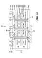
- FIG. 10 depicts FIG. 3, showing a metal pattern coupled to, and below, the top surface of the substrate.
- FIG. 11 depicts FIG. 3, showing a metal pattern within an interior portion of the substrate.
- FIG. 12 depicts FIG. 10, after a semiconductor chip has been coupled to the substrate.
- FIG. 3 illustrates a front cross-sectional view of an electronic structure 90 comprising an organic substrate 30 that includes an organic material, a metal structure 32 on a top surface 33 of the organic substrate 30 , and a metal structure 36 on a bottom surface 37 of the organic substrate 30 , in accordance with a preferred embodiment of the present invention.
- the metal structure 32 may include a metal plating (e.g., such as a copper plating) on at least one plated blind via 34 , and any conductive circuitization (not shown) on the top surface 33 .
- the plating on the plated blind via 34 is intended to be conductively coupled to an electronic device, such as the semiconductor chip 76 shown infra in FIG. 12 .
- the metal structure 36 may include metal pads, such as ball grid array (BGA) pads (see, e.g., FIG. 4 for an illustration of BGA pads), and any conductive circuitization (not shown) on the bottom surface 37 .
- BGA pads are intended to be conductively coupled to an electronic assembly such as a circuit card.
- the metal structure 32 and the metal structure 36 may be conductively coupled by any internal conductive structure within the organic substrate 30 , such as a plated though hole (PTH) 40 , together with a metal pad 41 conductively interfacing the metal structure 32 with the PTH 40 , and a metal pad 42 conductively interfacing the metal structure 36 with the PTH 40 .
- PTH plated though hole
- the metal structure 32 could each be conductively coupled to a first plated blind extending into an interior level of the organic substrate 30
- the metal structure 36 could be conductively coupled to into a second plated blind extending into the interior level, such that the first and second blind vias are coupled by interfacing conductive circuitization at the interior level.
- FIG. 3 shows the organic substrate 30 as comprising four dielectric layers: dielectric layer 44 denoted as a top layer that is included within the top surface 33 , dielectric layer 48 denoted as a bottom layer that is included within the bottom surface 37 , and dielectric layers 45 and 46 within a region 47 , wherein the region 47 interfaces with dielectric layers 44 and 48 .
- the region 47 (which comprises dielectric layers 45 and 46 as stated supra) includes the organic dielectric material. Additionally, the region 47 includes a thermally conductive layer 52 with the dielectric layers 45 and 46 on opposing surfaces 53 and 54 , respectively, of the thermally conductive layer 52 .
- the dielectric layer 45 includes a signal plane 55 and a power plane 56 , wherein the signal plane 55 is positioned between the thermally conductive layer 52 and the power plane 56 .
- a power plane comprises a continuous sheet of conductive material (e.g., copper) having at least one through hole.
- a signal plane comprises a layer of shielded signal conductors.
- the dielectric layer 46 includes a signal plane 57 and a power plane 58 , wherein the signal plane 57 is positioned between the thermally conductive layer 52 and the power plane 58 .
- the dielectric layers 44 and 48 each have a thickness preferably between about 40 microns and about 60 microns.
- the dielectric layers 44 and 48 provide a structural stability to the substrate 30 , inasmuch as the organic material in the dielectric layers 45 and 46 is soft compliant and thus may be difficult to handle in an absence of the more rigid dielectric layers 44 and 48 .
- the dielectric layers 44 and 48 each preferably include a dielectric material having a CTE that by no more than a factor of about 3 as the temperature increases from just below to just above the glass transition temperature (T g ) of the dielectric material of the dielectric layers 44 and 48 .
- a preferred dielectric material for the dielectric layers 44 and 48 includes a resin having an allylated polyphenylene ether (APPE) having T g of about 210° C. and characterized by a CTE increase of a factor of about 2.5 as the temperature increases from just below to just above T g .
- a particularly useful APPE for the dielectric layers 44 and 48 is an APPE resin coated on a copper foil, made by the Asahi Chemical Company of Japan and identified as Asahi product number PC5103.
- the substrate 30 remains somewhat compliant, and its structural stability may be further enhanced with a stiffener ring 50 bonded to an outer portion, such as an outer perimeter portion as shown in FIG. 3, of the top surface 33 of the organic substrate 30 by use of an interfacing adhesive 51 .
- the CTE of the stiffener ring 50 should preferably not differ by more than about 10% from the spatially average CTE of a composite structure of: the organic substrate 30 , the dielectric layer 44 , and the dielectric layer 48 .
- the thermally conductive layer 52 preferably has a coefficient of thermal expansion (CTE) between about 4 ppm/° C.
- a spatially averaged CTE of said composite structure is between about 10 ppm/° C. and about 12 ppm/° C.
- a suitable material for the stiffener ring 50 is, inter alia, 430 series stainless steel having a CTE of 10.0 ppm/° C.
- the dielectric layers 45 and 46 may be laminated to the thermally conductive layer 52 by, inter alia, placing the layers 45 and 46 on the opposing surfaces 53 and 54 of the thermally conductive layer 52 , to form a sandwich with the thermally conductive layer 52 as a middle layer of the sandwich.
- a pressure is applied to the sandwich, such as by using a lamination press. The pressure is between about 1000 psi and about 2000 psi at a temperature between about 305° C. and about 400° C.
- the PTH 40 which passes through the region 47 , may be formed by, inter alia, laser or mechanical drilling to form a via.
- a thin (e.g., 1 to 3 microns) metal e.g., copper
- a seeding material such as palladium to promote electroless adhesion of the metal to the via wall.
- a thicker (e.g., 1 mil) layer of the metal e.g., copper is electroplated over the electroless coat of the metal.
- other metal plating techniques known to one of ordinary skill in the art, may be used.
- the dielectric layers 44 and 48 may be laminated on the dielectric layers 45 and 46 , respectively, by any method known to one of ordinary skill in the art, in accordance with the particular dielectric material used in the dielectric layers 44 and 48 .
- the dielectric layers 44 and 48 if including the allylated polyphenylene ether (APPE) coated on a copper foil such as the Asahi resin PC5103, may be formed on the dielectric layers 45 and 46 , respectively, by pressurization in a range of about 1000 psi to about 2000 psi at an elevated temperature between about 180° C. and about 210° C. for a time of at least about 90 minutes.
- APSE allylated polyphenylene ether
- the pressurization and elevated temperatures causes the APPE resin to flow and become cured, resulting in lamination of the the dielectric layers 44 and 48 to the dielectric layers 45 and 46 , respectively.
- the copper foils are removed in any manner known to one of ordinary skill in the art, such as by etching.
- the plated blind via 34 may be formed by any method known to one of ordinary skill in the art, such as by laser drilling into the dielectric layer 44 down to the metal pad 41 to form a via, followed by electroless plating of metal (e.g., copper) on seeded surfaces (e.g., palladium seeded surfaces) of the via to form an electroless layer of the metal. After the electroless plating, the metal (e.g., copper) is electroplated over the electroless layer to form the plated blind via 34 .
- metal e.g., copper
- C 1 and A 1 denote the CTE and surface area of the metal structure 32 , respectively.
- C 2 and A 2 denote the CTE and surface area of the metal structure 36 , respectively.
- the values of C 1 , A 1 , C 2 , and A 2 are at ambient room temperature. It is assumed that C 2 A 2 exceeds C 1 A 1 . Under the preceding assumption and upon a heating of the substrate 30 , the top surface 33 will bow (or bulge) upward in a direction 28 , due to a thermal expansion imbalance between metalizations of the metal structure 32 and the metal structure 36 in consideration of the stiffener ring 50 , as explained supra in the “Related Arts” section.
- the organic structure 30 in FIG. 3 is illustrative and many other alternative structures are within the scope of the present invention.
- the structure 30 may have any number of dielectric layers, including as few as one dielectric layer.
- any of the thermally conductive layer 52 , the signal planes 55 and 57 , and the power planes 56 and 58 may or may not be present.
- words such as “top,” “bottom,” “up,” and “down,” do not imply a directional orientation with respect to a radial direction from a center of the Earth, but rather serve to orient the reader in viewing the Figures in this patent application.
- FIG. 4 shows a bottom view of the organic substrate 30 of FIG. 3, showing BGA pads illustrating the second metal structure 36 on the bottom surface 37 of the organic substrate 30 .
- Each of the 15 BGA pads of the second metal structure 36 in FIG. 4 is intended to contact a BGA solder ball for coupling the organic substrate 30 to a circuit card.
- the BGA pad pattern in FIG. 4 is an example of the second metal structure 36 .
- Any geometric configuration of metal on the bottom surface 37 of the organic substrate 30 may represent the second metal structure 36 .
- FIG. 5 illustrates a top view of the organic substrate 30 of FIG. 3, along with the stiffener ring 50 , showing a metal pattern 61 coupled to unoccupied space at or adjacent to (see discussion following description of FIGS. 9-11 for a definition of “adjacent to”) the top surface 33 , in order to compensate for an imbalance between C 1 A 1 (of the top surface 33 ) and C 2 A 2 (of the bottom surface 37 ).
- the metal pattern 61 has a CTE and surface area of C 3 and A 3 , respectively, such that (C 2 A 2 ⁇ C 1 A 1 ⁇ C 3 A 3 ) is less than (C 2 A 2 ⁇ C 1 A 1 ) in magnitude.
- the value of C 3 and A 3 are at ambient room temperature.
- the metal pattern 61 compensates partially or fully for a thermal imbalance between C 1 A 1 and C 2 A 2 .
- C 2 A 2 and (C 3 A 3 +C 1 A 1 ) should differ in magnitude by no more than about 20%, and preferably by no more than about 10%.
- the preceding condition takes the form of having A 2 and (A 3 +A 1 ) differ in magnitude by no more than about 20%, and preferably by no more than about 10%. If the first metal structure 32 , the second metal structure 36 , and the metal pattern 61 are each comprised of the same metal, then C 1 , C 2 , and C 3 are about equal.
- first metal structure 32 , the second metal structure 36 , and the metal pattern 61 may include different metals, and C 1 , C 2 , and C 3 may accordingly differ.
- Copper which has a CTE of about 17 ppm/° C.
- Other metal suitable for the metal pattern 61 include nickel, which has a CTE of about 17 or 18 ppm/° C., and aluminum, which has a CTE of about 20 ppm/° C.
- the thicknesses of the first metal structure 32 , the second metal structure 36 , and the metal pattern 61 are preferably comparable, and deviations in thickness within about 10% will not significantly impact the effectiveness of the thermal balancing scheme described supra. If said thickness deviations exceed about 10%, then the surface exposed A 3 of the metal pattern 61 may be adjusted to deviate from the preceding formula of balancing (A 3 C 3 +A 1 C 1 ) against A 2 C 2 , to whatever extent is necessary for achieving a desired level of thermal balancing.
- Said adjusting of A 3 may be accomplished by testing, and without undue experimentation, by recognizing that a smaller thickness in the metal pattern 61 allows more thermal expansion length of the metal pattern 61 parallel to the top surface 33 of the organic substrate 30 than does a larger thickness, for a given surface area A 3 .
- a thickness in the metal pattern 61 that is too large, which inhibits expansion parallel to the top surface 33 may be compensated for by increasing the surface area A 3 .
- the metal pattern 61 may be coupled to any unoccupied space at the top surface 33 .
- the metal pattern 61 is insulatively isolated from any other conductive structure on or within the substrate 30 .
- the metal pattern 61 has no electrical function, and serves the particularized function of balancing thermal expansion of metalization on the top and bottom surfaces 33 and 37 , respectively, so as to reduce or eliminate flexing of the substrate 30 when subjected to an elevated temperature.
- the effectiveness of the metal pattern 61 for thermal balancing purposes is insensitive to a spatial distribution of the metal pattern 61 on the top surface 33 , provided that a combined spatial distribution of the metal pattern 61 and the metal structure 32 on the top surface 33 is not highly skewed in comparison with a spatial distribution of the metal structure 36 on the bottom surface 37 .
- the geometry of the metal pattern 61 is arbitrary, and metal of any geometry may be coupled to the top surface 33 to effectuate thermal balancing, provided that such metal is insulatively isolated from any other conductive structure on or within the substrate 30 .
- Other examples of metal patterns that may be coupled to unoccupied space at or adjacent to (see discussion following description of FIGS. 9-11 for a definition of “adjacent to”) the top surface 33 are shown in FIGS. 6, 7 , and 8 , namely metal patterns 62 , 63 , and 64 , respectively.
- FIG. 6 shows the metal pattern 62 having a circular geometric arrangement.
- FIG. 7 shows the metal pattern 63 having a two-dimensional rectangular geometric arrangement.
- FIG. 8 shows the metal pattern 64 having a random geometric arrangement as to both shape and location.
- An insulatively metal pattern (e.g., any of the metal patterns 61 , 62 , 63 , 64 in FIG. 5-8, respectively) that is coupled to the top surface 33 of the organic substrate 30 for thermal balancing purposes, may be formed either above or below the top surface 33 as shown in FIGS. 9 and 10, respectively.
- FIG. 9 illustrates FIG. 3, showing a metal pattern 65 above, and coupled to, the top surface 33 of the organic substrate 30 .
- the metal pattern 65 may be formed by any method known to one of ordinary skill in the art. If metal such as copper is utilized for the metal pattern 61 , for example, then the metal pattern 65 may be formed by: bonding a preformed sheet of the metal (e.g., copper) on the top surface 33 , reducing the thickness of the preformed sheet of the metal to the desired thickness, applying photoresist and photolithographically exposing portions of the metal sheet to radiation (e.g., ultraviolet radiation), chemically developing away unexposed photoresist and the metal underneath the unexposed photoresist, and stripping away the exposed photoresist, such that the metal pattern 65 has been generated and is insulatively isolated from any other conductive structure on or within the substrate 30 .
- radiation e.g., ultraviolet radiation
- both the metal structure 32 and the metal pattern 65 each include the same metal (e.g., copper), then the metal pattern 65 may be formed concurrent with, and by the same process as, formation of circuitization associated with the metal structure 32 on the top surface 33 , which would enable the metal pattern 65 to be formed at little or no extra cost inasmuch as the circuitization associated with the metal structure 32 would be formed regardless of whether the metal pattern 65 is also formed.
- the metal pattern 65 may be formed concurrent with, and by the same process as, formation of circuitization associated with the metal structure 32 on the top surface 33 , which would enable the metal pattern 65 to be formed at little or no extra cost inasmuch as the circuitization associated with the metal structure 32 would be formed regardless of whether the metal pattern 65 is also formed.
- the metal pattern 65 may be formed by electroplating or sputter deposition.
- the thickness of the metal pattern 61 may be reduced as needed by any method known to one of ordinary skill in the art.
- the metal pattern 65 may be formed by the same method described supra for copper, except that the thickness of the preformed sheet of aluminum cannot be easily reduced.
- the preformed sheet of aluminum should have a thickness that is close to desired thickness of the metal pattern 61 .
- FIG. 10 illustrates FIG. 3, showing a metal pattern 66 below, and coupled to, the top surface 33 of the organic substrate 30 .
- the metal pattern 66 may be formed by any method known to one of ordinary skill in the art, such as by laser-drilling isolated cavities (i.e., blind vias) in the dielectric layer 44 , and filling the cavities with the metal (of the intended metal pattern 66 ) by electroless plating on seeded surfaces (e.g., palladium seeded surfaces) of the cavities, followed by electroplating the metal to fill the cavities to the level of the top surface 33 .
- seeded surfaces e.g., palladium seeded surfaces
- FIG. 11 illustrates FIG. 3, showing a metal pattern 67 coupled to a top surface 49 of the dielectric layer 45 .
- the metal pattern 67 may be formed by any method known to one of ordinary skill in the art, such as by the same example method that was described for forming the metal pattern 65 in conjunction with FIG. 9 . It should be noted that the metal pattern 67 could be formed concurrent with, and by the same process as, formation of the metal pad 41 .
- FIGS. 9-11 collectively illustrate that a metal pattern of the present invention (e.g., the metal pattern 65 , 66 , or 67 of FIG. 9, 10 , or 11 , respectively) should be positioned “adjacent to” the top surface 33 of the organic substrate 30 , wherein “adjacent to” includes being coupled to (e.g., FIGS. 9-10) or being proximate to (e.g., FIG. 11 ). “Proximate to” means being located at a distance from the top surface 33 than does not exceed the thickness of the dielectric layer 44 . As stated supra, the thickness of the dielectric layer 44 is preferably between about 40 microns and about 60 microns.
- FIG. 12 illustrates FIG. 10 after a semiconductor chip 76 has been coupled to the organic substrate 30 by any solderably coupling process known to one of ordinary skill in the art.
- the plated blind vias 34 may be filled with a solder 70 shown in FIG. 12, and conductive contacts 72 of the semiconductor chip 76 are placed in contact with the solder 70 .
- the solder 70 is thus conductively coupled to the metal structure 32 .
- the solder 70 is then reflowed at a temperature above the melting temperature of the solder 70 , and below the melting point of the conductive contacts 72 , such that the reflowed solder 70 conductively abuts all conductive contacts 72 , and adhesively and conductively couples with all conductive contacts 72 as the reflowed solder 70 cools.
- the semiconductor chip 76 is conductively coupled to the metal structure 32 at all conductive contacts 72 of the semiconductor chip 76 .
- the conductive contacts 72 are Controlled Collapse Chip Connection (C 4 ) solder balls comprising solder material having a composition of about 97% lead and about 3% tin with a melting temperature of about 310° C.
- the solder 70 is a low-melt lead-tin solder with a melting temperature below about 230° C. and at least the melting point of 183° C. of the eutectic composition of about 63% lead and about 37% tin.
- the solder 70 may have any of various geometric shapes known to those of ordinary skill in the art, such as solder balls and solder columns.
- a thermal expansion mismatch (i.e., C 2 A 2 >C 1 A 1 ) between the solder structure 36 on the bottom surface 37 and solder structure 32 on the top surface 33 would cause the top surface 33 to bow or bulge upward in the direction 28 .
- the present invention reduces or eliminates the thermal mismatch by adding the metal pattern 66 to satisfy the condition that (C 2 A 2 ⁇ C 1 A 1 ⁇ C 3 A 3 ) is less than (C 2 A 2 ⁇ C 1 A 1 ) in magnitude.
- C 2 A 2 and (C 3 A 3 +C 1 A 1 ) should differ in magnitude by no more than about 20%, and preferably by no more than about 10%.
- the present invention is capable of constraining bowing of the substrate 30 to within about 1 mil, and reducing the upward bowing by a factor of at least 2 in comparison with the bowing that would have occurred had the metal pattern 66 not been included (see FIG. 2 and accompanying discussion for a definition of the bowing B).
- the present invention is capable of constraining bowing of the substrate 30 to within about 1 ⁇ 2 mil.
- the semiconductor chip 76 in FIG. 12 is generally representative of an electronic device having a plurality of conductive contacts such as the conductive contacts 72 . Any such electronic device that could be solderably coupled to the substrate 30 may substitute for the semiconductor chip 76 in FIG. 12 .
- the metal pattern 66 is electrically insulated from any other conductive structure on or within the substrate 30 and thus does not participate in any electrical conduction functionality of the substrate 30 . While the metal pattern 66 is below and coupled to the top surface 33 , the metal pattern 66 could be replaced by the metal pattern 65 depicted in FIG. 9 as above and coupled to the top surface 33 . Similarly, the metal pattern 66 could be replaced by the metal pattern 67 depicted in FIG. 11 . Thus, the semiconductor chip 76 could be coupled to the organic substrate 30 in the configurations of FIGS. 9 and 11 in the same manner as the semiconductor chip 76 could be coupled to the configuration of FIG. 10 . Additionally, the metal pattern 66 could have any geometrical shape, such as the geometrical shape of any of the metal patterns 61 - 64 shown in FIGS. 5-8, respectively.
Landscapes
- Engineering & Computer Science (AREA)
- Microelectronics & Electronic Packaging (AREA)
- Physics & Mathematics (AREA)
- Condensed Matter Physics & Semiconductors (AREA)
- General Physics & Mathematics (AREA)
- Computer Hardware Design (AREA)
- Power Engineering (AREA)
- Wire Bonding (AREA)
Abstract
Description
Claims (17)
Priority Applications (3)
| Application Number | Priority Date | Filing Date | Title |
|---|---|---|---|
| US09/503,395 US6497943B1 (en) | 2000-02-14 | 2000-02-14 | Surface metal balancing to reduce chip carrier flexing |
| US09/691,935 US6528179B1 (en) | 2000-02-14 | 2000-10-19 | Reduction of chip carrier flexing during thermal cycling |
| US10/262,023 US6818972B2 (en) | 2000-02-14 | 2002-09-30 | Reduction of chip carrier flexing during thermal cycling |
Applications Claiming Priority (1)
| Application Number | Priority Date | Filing Date | Title |
|---|---|---|---|
| US09/503,395 US6497943B1 (en) | 2000-02-14 | 2000-02-14 | Surface metal balancing to reduce chip carrier flexing |
Related Child Applications (1)
| Application Number | Title | Priority Date | Filing Date |
|---|---|---|---|
| US09/691,935 Continuation-In-Part US6528179B1 (en) | 2000-02-14 | 2000-10-19 | Reduction of chip carrier flexing during thermal cycling |
Publications (1)
| Publication Number | Publication Date |
|---|---|
| US6497943B1 true US6497943B1 (en) | 2002-12-24 |
Family
ID=24001911
Family Applications (1)
| Application Number | Title | Priority Date | Filing Date |
|---|---|---|---|
| US09/503,395 Expired - Fee Related US6497943B1 (en) | 2000-02-14 | 2000-02-14 | Surface metal balancing to reduce chip carrier flexing |
Country Status (1)
| Country | Link |
|---|---|
| US (1) | US6497943B1 (en) |
Cited By (76)
| Publication number | Priority date | Publication date | Assignee | Title |
|---|---|---|---|---|
| US20020139578A1 (en) * | 2001-03-28 | 2002-10-03 | International Business Machines Corporation | Hyperbga buildup laminate |
| US20030102570A1 (en) * | 2000-08-31 | 2003-06-05 | Hitachi, Ltd. | Electronic device and a method of manufacturing the same |
| US20030116857A1 (en) * | 2001-12-26 | 2003-06-26 | Fujitsu Limited | Circuit substrate and method for fabricating the same |
| US6639302B2 (en) * | 2002-03-20 | 2003-10-28 | International Business Machines Corporation | Stress reduction in flip-chip PBGA packaging by utilizing segmented chip carries |
| US20030215619A1 (en) * | 2002-05-14 | 2003-11-20 | Shinko Electric Industries Co., Ltd. | Metal core substrate and process for manufacturing same |
| US20040093344A1 (en) * | 2001-05-25 | 2004-05-13 | Ben Berger | Method and system for mapping enterprise data assets to a semantic information model |
| US20040104463A1 (en) * | 2002-09-27 | 2004-06-03 | Gorrell Robin E. | Crack resistant interconnect module |
| US20040124004A1 (en) * | 2002-12-30 | 2004-07-01 | Rajendran Nair | Decoupled signal-power substrate architecture |
| US20040129453A1 (en) * | 2003-01-07 | 2004-07-08 | Boggs David W. | Electronic substrate with direct inner layer component interconnection |
| US20040219342A1 (en) * | 2003-01-07 | 2004-11-04 | Boggs David W. | Electronic substrate with direct inner layer component interconnection |
| US20040262756A1 (en) * | 2003-06-30 | 2004-12-30 | Robert Nickerson | Ball grid array copper balancing |
| US20050149484A1 (en) * | 2001-05-25 | 2005-07-07 | Joshua Fox | Run-time architecture for enterprise integration with transformation generation |
| US6930256B1 (en) * | 2002-05-01 | 2005-08-16 | Amkor Technology, Inc. | Integrated circuit substrate having laser-embedded conductive patterns and method therefor |
| US20050234889A1 (en) * | 2001-05-25 | 2005-10-20 | Joshua Fox | Method and system for federated querying of data sources |
| US20050240606A1 (en) * | 2001-05-25 | 2005-10-27 | Joseph Edelstein | Data query and location through a central ontology model |
| US6992379B2 (en) * | 2001-09-05 | 2006-01-31 | International Business Machines Corporation | Electronic package having a thermal stretching layer |
| US20060024865A1 (en) * | 2001-02-05 | 2006-02-02 | Underwood Jeffrey A | Method for shielding printed circuit board circuits |
| US20060064666A1 (en) * | 2001-05-25 | 2006-03-23 | Amaru Ruth M | Business rules for configurable metamodels and enterprise impact analysis |
| US20060231943A1 (en) * | 2005-04-14 | 2006-10-19 | Chin-Tien Chiu | Rigid wave pattern design on chip carrier substrate and printed circuit board for semiconductor and electronic sub-system packaging |
| US7145238B1 (en) | 2004-05-05 | 2006-12-05 | Amkor Technology, Inc. | Semiconductor package and substrate having multi-level vias |
| US20070075142A1 (en) * | 2005-09-30 | 2007-04-05 | Symbol Technologies, Inc. | Mobile computer with integrated UHF RFID reader |
| US7334326B1 (en) | 2001-06-19 | 2008-02-26 | Amkor Technology, Inc. | Method for making an integrated circuit substrate having embedded passive components |
| CN100388481C (en) * | 2003-12-24 | 2008-05-14 | 上海华虹Nec电子有限公司 | Integrate circuit chip structure |
| US20080142256A1 (en) * | 2003-05-23 | 2008-06-19 | Fujitsu Limited | Wiring board manufacturing method |
| US20080313232A1 (en) * | 2001-05-25 | 2008-12-18 | International Business Machines Corporation | Data Query and Location Through a Central Ontology Model |
| US7670962B2 (en) | 2002-05-01 | 2010-03-02 | Amkor Technology, Inc. | Substrate having stiffener fabrication method |
| US7750250B1 (en) | 2006-12-22 | 2010-07-06 | Amkor Technology, Inc. | Blind via capture pad structure |
| US7752752B1 (en) | 2007-01-09 | 2010-07-13 | Amkor Technology, Inc. | Method of fabricating an embedded circuit pattern |
| US7825520B1 (en) | 2006-11-16 | 2010-11-02 | Amkor Technology, Inc. | Stacked redistribution layer (RDL) die assembly package |
| US7911037B1 (en) | 2006-10-04 | 2011-03-22 | Amkor Technology, Inc. | Method and structure for creating embedded metal features |
| US7960827B1 (en) | 2009-04-09 | 2011-06-14 | Amkor Technology, Inc. | Thermal via heat spreader package and method |
| US8018068B1 (en) | 2004-03-23 | 2011-09-13 | Amkor Technology, Inc. | Semiconductor package including a top-surface metal layer for implementing circuit features |
| US20110259627A1 (en) * | 2006-10-30 | 2011-10-27 | Samsung Electro-Mechanics Co., Ltd. | Circuit board with buried circuit pattern |
| US8222538B1 (en) | 2009-06-12 | 2012-07-17 | Amkor Technology, Inc. | Stackable via package and method |
| US8294276B1 (en) | 2010-05-27 | 2012-10-23 | Amkor Technology, Inc. | Semiconductor device and fabricating method thereof |
| US8300423B1 (en) | 2010-05-25 | 2012-10-30 | Amkor Technology, Inc. | Stackable treated via package and method |
| US8323771B1 (en) | 2007-08-15 | 2012-12-04 | Amkor Technology, Inc. | Straight conductor blind via capture pad structure and fabrication method |
| US8338229B1 (en) | 2010-07-30 | 2012-12-25 | Amkor Technology, Inc. | Stackable plasma cleaned via package and method |
| US8337657B1 (en) | 2010-10-27 | 2012-12-25 | Amkor Technology, Inc. | Mechanical tape separation package and method |
| US8341835B1 (en) | 2002-05-01 | 2013-01-01 | Amkor Technology, Inc. | Buildup dielectric layer having metallization pattern semiconductor package fabrication method |
| US8471154B1 (en) | 2009-08-06 | 2013-06-25 | Amkor Technology, Inc. | Stackable variable height via package and method |
| US8482134B1 (en) | 2010-11-01 | 2013-07-09 | Amkor Technology, Inc. | Stackable package and method |
| US8525336B2 (en) * | 2011-10-17 | 2013-09-03 | Siliconware Precision Industries Co., Ltd. | Semiconductor package and method of fabricating the same |
| US8525318B1 (en) | 2010-11-10 | 2013-09-03 | Amkor Technology, Inc. | Semiconductor device and fabricating method thereof |
| US8536462B1 (en) | 2010-01-22 | 2013-09-17 | Amkor Technology, Inc. | Flex circuit package and method |
| US8535961B1 (en) | 2010-12-09 | 2013-09-17 | Amkor Technology, Inc. | Light emitting diode (LED) package and method |
| US8557629B1 (en) | 2010-12-03 | 2013-10-15 | Amkor Technology, Inc. | Semiconductor device having overlapped via apertures |
| US8623753B1 (en) | 2009-05-28 | 2014-01-07 | Amkor Technology, Inc. | Stackable protruding via package and method |
| US8633598B1 (en) | 2011-09-20 | 2014-01-21 | Amkor Technology, Inc. | Underfill contacting stacking balls package fabrication method and structure |
| US8653674B1 (en) | 2011-09-15 | 2014-02-18 | Amkor Technology, Inc. | Electronic component package fabrication method and structure |
| US8717775B1 (en) | 2010-08-02 | 2014-05-06 | Amkor Technology, Inc. | Fingerprint sensor package and method |
| US8796561B1 (en) | 2009-10-05 | 2014-08-05 | Amkor Technology, Inc. | Fan out build up substrate stackable package and method |
| US8826531B1 (en) | 2005-04-05 | 2014-09-09 | Amkor Technology, Inc. | Method for making an integrated circuit substrate having laminated laser-embedded circuit layers |
| US8872329B1 (en) * | 2009-01-09 | 2014-10-28 | Amkor Technology, Inc. | Extended landing pad substrate package structure and method |
| US8890329B2 (en) | 2011-04-26 | 2014-11-18 | Amkor Technology, Inc. | Semiconductor device |
| US8937381B1 (en) | 2009-12-03 | 2015-01-20 | Amkor Technology, Inc. | Thin stackable package and method |
| US20150029689A1 (en) * | 2013-07-26 | 2015-01-29 | Shinko Electric Industries Co., Ltd. | Bump structure, wiring substrate, semiconductor apparatus and bump structure manufacturing method |
| US9013011B1 (en) | 2011-03-11 | 2015-04-21 | Amkor Technology, Inc. | Stacked and staggered die MEMS package and method |
| US9029962B1 (en) | 2011-10-12 | 2015-05-12 | Amkor Technology, Inc. | Molded cavity substrate MEMS package fabrication method and structure |
| US9391043B2 (en) | 2012-11-20 | 2016-07-12 | Amkor Technology, Inc. | Semiconductor device and manufacturing method thereof |
| US9543242B1 (en) | 2013-01-29 | 2017-01-10 | Amkor Technology, Inc. | Semiconductor package and fabricating method thereof |
| US20170178987A1 (en) * | 2015-12-16 | 2017-06-22 | Siddarth Kumar | Warpage controlled package and method for same |
| US9691734B1 (en) | 2009-12-07 | 2017-06-27 | Amkor Technology, Inc. | Method of forming a plurality of electronic component packages |
| US9691635B1 (en) | 2002-05-01 | 2017-06-27 | Amkor Technology, Inc. | Buildup dielectric layer having metallization pattern semiconductor package fabrication method |
| US9704747B2 (en) | 2013-03-29 | 2017-07-11 | Amkor Technology, Inc. | Semiconductor device and manufacturing method thereof |
| US9704842B2 (en) | 2013-11-04 | 2017-07-11 | Amkor Technology, Inc. | Interposer, manufacturing method thereof, semiconductor package using the same, and method for fabricating the semiconductor package |
| US9721872B1 (en) | 2011-02-18 | 2017-08-01 | Amkor Technology, Inc. | Methods and structures for increasing the allowable die size in TMV packages |
| US9748154B1 (en) | 2010-11-04 | 2017-08-29 | Amkor Technology, Inc. | Wafer level fan out semiconductor device and manufacturing method thereof |
| US9899305B1 (en) * | 2017-04-28 | 2018-02-20 | Taiwan Semiconductor Manufacturing Company Ltd. | Semiconductor package structure |
| CN107787113A (en) * | 2017-10-17 | 2018-03-09 | 广东欧珀移动通信有限公司 | Circuit board assemblies and mobile terminal |
| US9960328B2 (en) | 2016-09-06 | 2018-05-01 | Amkor Technology, Inc. | Semiconductor device and manufacturing method thereof |
| US20190019774A1 (en) * | 2007-12-18 | 2019-01-17 | Micron Technology, Inc. | Methods of fluxless micro-piercing of solder balls, and resulting devices |
| US20190326261A1 (en) * | 2016-11-30 | 2019-10-24 | Shenzhen Xiuyuan Electronic Technology Co., Ltd | Integrated Circuit Multichip Stacked Packaging Structure and Method |
| WO2020097767A1 (en) * | 2018-11-12 | 2020-05-22 | 北京比特大陆科技有限公司 | Circuit board and supercomputing equipment |
| US10811277B2 (en) | 2004-03-23 | 2020-10-20 | Amkor Technology, Inc. | Encapsulated semiconductor package |
| US11081370B2 (en) | 2004-03-23 | 2021-08-03 | Amkor Technology Singapore Holding Pte. Ltd. | Methods of manufacturing an encapsulated semiconductor device |
Citations (8)
| Publication number | Priority date | Publication date | Assignee | Title |
|---|---|---|---|---|
| US5120573A (en) * | 1988-09-28 | 1992-06-09 | Hitachi, Ltd. | Process for producing metal/polyimide composite article |
| US5886877A (en) * | 1995-10-13 | 1999-03-23 | Meiko Electronics Co., Ltd. | Circuit board, manufacturing method therefor, and bump-type contact head and semiconductor component packaging module using the circuit board |
| US5888631A (en) | 1996-11-08 | 1999-03-30 | W. L. Gore & Associates, Inc. | Method for minimizing warp in the production of electronic assemblies |
| US5900312A (en) | 1996-11-08 | 1999-05-04 | W. L. Gore & Associates, Inc. | Integrated circuit chip package assembly |
| US6204456B1 (en) * | 1998-09-24 | 2001-03-20 | International Business Machines Corporation | Filling open through holes in a multilayer board |
| US6204453B1 (en) * | 1998-12-02 | 2001-03-20 | International Business Machines Corporation | Two signal one power plane circuit board |
| US6329713B1 (en) * | 1998-10-21 | 2001-12-11 | International Business Machines Corporation | Integrated circuit chip carrier assembly comprising a stiffener attached to a dielectric substrate |
| US6359235B1 (en) * | 1999-07-30 | 2002-03-19 | Kyocera Corporation | Electrical device mounting wiring board and method of producing the same |
-
2000
- 2000-02-14 US US09/503,395 patent/US6497943B1/en not_active Expired - Fee Related
Patent Citations (8)
| Publication number | Priority date | Publication date | Assignee | Title |
|---|---|---|---|---|
| US5120573A (en) * | 1988-09-28 | 1992-06-09 | Hitachi, Ltd. | Process for producing metal/polyimide composite article |
| US5886877A (en) * | 1995-10-13 | 1999-03-23 | Meiko Electronics Co., Ltd. | Circuit board, manufacturing method therefor, and bump-type contact head and semiconductor component packaging module using the circuit board |
| US5888631A (en) | 1996-11-08 | 1999-03-30 | W. L. Gore & Associates, Inc. | Method for minimizing warp in the production of electronic assemblies |
| US5900312A (en) | 1996-11-08 | 1999-05-04 | W. L. Gore & Associates, Inc. | Integrated circuit chip package assembly |
| US6204456B1 (en) * | 1998-09-24 | 2001-03-20 | International Business Machines Corporation | Filling open through holes in a multilayer board |
| US6329713B1 (en) * | 1998-10-21 | 2001-12-11 | International Business Machines Corporation | Integrated circuit chip carrier assembly comprising a stiffener attached to a dielectric substrate |
| US6204453B1 (en) * | 1998-12-02 | 2001-03-20 | International Business Machines Corporation | Two signal one power plane circuit board |
| US6359235B1 (en) * | 1999-07-30 | 2002-03-19 | Kyocera Corporation | Electrical device mounting wiring board and method of producing the same |
Non-Patent Citations (3)
| Title |
|---|
| "High Performance Carrier Technology", by Heck et al, 1993 International Electronics Packaging Conference, San Diego, California, vol. one. No Month. |
| "High Performance Carrier Technology: Materials And Fabrication", by Light et al, 1993 International Electronics Packaging Conference, San Diego, California, vol. one. No Month. |
| "Process Considerations in the Fabrication of Teflon Printed Circuit Boards", by Light et al, 1994 Proceedings, 44 Electronic Components & Technology Conference, 5/1994. |
Cited By (153)
| Publication number | Priority date | Publication date | Assignee | Title |
|---|---|---|---|---|
| US20030102570A1 (en) * | 2000-08-31 | 2003-06-05 | Hitachi, Ltd. | Electronic device and a method of manufacturing the same |
| US7132357B2 (en) * | 2001-02-05 | 2006-11-07 | Motorola, Inc. | Method for shielding printed circuit board circuits |
| US20060024865A1 (en) * | 2001-02-05 | 2006-02-02 | Underwood Jeffrey A | Method for shielding printed circuit board circuits |
| US6879492B2 (en) * | 2001-03-28 | 2005-04-12 | International Business Machines Corporation | Hyperbga buildup laminate |
| US20020139578A1 (en) * | 2001-03-28 | 2002-10-03 | International Business Machines Corporation | Hyperbga buildup laminate |
| US7921098B2 (en) | 2001-05-25 | 2011-04-05 | International Business Machines Corporation | Data query and location through a central ontology model |
| US20050234889A1 (en) * | 2001-05-25 | 2005-10-20 | Joshua Fox | Method and system for federated querying of data sources |
| US8548938B2 (en) | 2001-05-25 | 2013-10-01 | International Business Machines Corporation | Business rules for configurable metamodels and enterprise impact analysis |
| US8412746B2 (en) | 2001-05-25 | 2013-04-02 | International Business Machines Corporation | Method and system for federated querying of data sources |
| US8060531B2 (en) | 2001-05-25 | 2011-11-15 | International Business Machines Corporation | Data query and location through a central ontology model |
| US7962503B2 (en) | 2001-05-25 | 2011-06-14 | International Business Machines Corporation | Data query and location through a central ontology model |
| US7930293B2 (en) | 2001-05-25 | 2011-04-19 | International Business Machines Corporation | Run-time architecture for enterprise integration with transformation generation |
| US20080313232A1 (en) * | 2001-05-25 | 2008-12-18 | International Business Machines Corporation | Data Query and Location Through a Central Ontology Model |
| US20090077051A1 (en) * | 2001-05-25 | 2009-03-19 | International Business Machines Corporation | Data Query and Location Through a Central Ontology Model |
| US20050149484A1 (en) * | 2001-05-25 | 2005-07-07 | Joshua Fox | Run-time architecture for enterprise integration with transformation generation |
| US7877421B2 (en) | 2001-05-25 | 2011-01-25 | International Business Machines Corporation | Method and system for mapping enterprise data assets to a semantic information model |
| US20040093344A1 (en) * | 2001-05-25 | 2004-05-13 | Ben Berger | Method and system for mapping enterprise data assets to a semantic information model |
| US20050240606A1 (en) * | 2001-05-25 | 2005-10-27 | Joseph Edelstein | Data query and location through a central ontology model |
| US20060064666A1 (en) * | 2001-05-25 | 2006-03-23 | Amaru Ruth M | Business rules for configurable metamodels and enterprise impact analysis |
| US7334326B1 (en) | 2001-06-19 | 2008-02-26 | Amkor Technology, Inc. | Method for making an integrated circuit substrate having embedded passive components |
| US6992379B2 (en) * | 2001-09-05 | 2006-01-31 | International Business Machines Corporation | Electronic package having a thermal stretching layer |
| US20030116857A1 (en) * | 2001-12-26 | 2003-06-26 | Fujitsu Limited | Circuit substrate and method for fabricating the same |
| US7139176B2 (en) * | 2001-12-26 | 2006-11-21 | Fujitsu Limited | Circuit substrate and method for fabricating the same |
| US6639302B2 (en) * | 2002-03-20 | 2003-10-28 | International Business Machines Corporation | Stress reduction in flip-chip PBGA packaging by utilizing segmented chip carries |
| US6989607B2 (en) | 2002-03-20 | 2006-01-24 | International Business Machines Corporation | Stress reduction in flip-chip PBGA packaging by utilizing segmented chips and/or chip carriers |
| US20040021205A1 (en) * | 2002-03-20 | 2004-02-05 | Krishna Darbha | Stress reduction in flip-chip PBGA packaging by utilizing segmented chips and/or chip carriers |
| US7671457B1 (en) | 2002-05-01 | 2010-03-02 | Amkor Technology, Inc. | Semiconductor package including top-surface terminals for mounting another semiconductor package |
| US7670962B2 (en) | 2002-05-01 | 2010-03-02 | Amkor Technology, Inc. | Substrate having stiffener fabrication method |
| US8026587B1 (en) | 2002-05-01 | 2011-09-27 | Amkor Technology, Inc. | Semiconductor package including top-surface terminals for mounting another semiconductor package |
| US8110909B1 (en) | 2002-05-01 | 2012-02-07 | Amkor Technology, Inc. | Semiconductor package including top-surface terminals for mounting another semiconductor package |
| US7312103B1 (en) | 2002-05-01 | 2007-12-25 | Amkor Technology, Inc. | Method for making an integrated circuit substrate having laser-embedded conductive patterns |
| US7185426B1 (en) | 2002-05-01 | 2007-03-06 | Amkor Technology, Inc. | Method of manufacturing a semiconductor package |
| US9691635B1 (en) | 2002-05-01 | 2017-06-27 | Amkor Technology, Inc. | Buildup dielectric layer having metallization pattern semiconductor package fabrication method |
| US9812386B1 (en) | 2002-05-01 | 2017-11-07 | Amkor Technology, Inc. | Encapsulated semiconductor package |
| US10461006B1 (en) | 2002-05-01 | 2019-10-29 | Amkor Technology, Inc. | Encapsulated semiconductor package |
| US8316536B1 (en) | 2002-05-01 | 2012-11-27 | Amkor Technology, Inc. | Multi-level circuit substrate fabrication method |
| US6930256B1 (en) * | 2002-05-01 | 2005-08-16 | Amkor Technology, Inc. | Integrated circuit substrate having laser-embedded conductive patterns and method therefor |
| US8341835B1 (en) | 2002-05-01 | 2013-01-01 | Amkor Technology, Inc. | Buildup dielectric layer having metallization pattern semiconductor package fabrication method |
| US8322030B1 (en) * | 2002-05-01 | 2012-12-04 | Amkor Technology, Inc. | Circuit-on-foil process for manufacturing a laminated semiconductor package substrate having embedded conductive patterns |
| US20030215619A1 (en) * | 2002-05-14 | 2003-11-20 | Shinko Electric Industries Co., Ltd. | Metal core substrate and process for manufacturing same |
| US6767616B2 (en) * | 2002-05-14 | 2004-07-27 | Shinko Electric Industries Co., Ltd. | Metal core substrate and process for manufacturing same |
| US20040104463A1 (en) * | 2002-09-27 | 2004-06-03 | Gorrell Robin E. | Crack resistant interconnect module |
| US7405364B2 (en) * | 2002-12-30 | 2008-07-29 | Intel Corporation | Decoupled signal-power substrate architecture |
| US20040124004A1 (en) * | 2002-12-30 | 2004-07-01 | Rajendran Nair | Decoupled signal-power substrate architecture |
| US20040129453A1 (en) * | 2003-01-07 | 2004-07-08 | Boggs David W. | Electronic substrate with direct inner layer component interconnection |
| US20040219342A1 (en) * | 2003-01-07 | 2004-11-04 | Boggs David W. | Electronic substrate with direct inner layer component interconnection |
| US7935891B2 (en) * | 2003-05-23 | 2011-05-03 | Fujitsu Limited | Wiring board manufacturing method |
| US20080142256A1 (en) * | 2003-05-23 | 2008-06-19 | Fujitsu Limited | Wiring board manufacturing method |
| US20070184644A1 (en) * | 2003-06-30 | 2007-08-09 | Intel Corporation | Ball grid array copper balancing |
| US20040262756A1 (en) * | 2003-06-30 | 2004-12-30 | Robert Nickerson | Ball grid array copper balancing |
| US7205649B2 (en) * | 2003-06-30 | 2007-04-17 | Intel Corporation | Ball grid array copper balancing |
| CN100388481C (en) * | 2003-12-24 | 2008-05-14 | 上海华虹Nec电子有限公司 | Integrate circuit chip structure |
| US11081370B2 (en) | 2004-03-23 | 2021-08-03 | Amkor Technology Singapore Holding Pte. Ltd. | Methods of manufacturing an encapsulated semiconductor device |
| US8227338B1 (en) | 2004-03-23 | 2012-07-24 | Amkor Technology, Inc. | Semiconductor package including a top-surface metal layer for implementing circuit features |
| US11094560B1 (en) | 2004-03-23 | 2021-08-17 | Amkor Technology Singapore Holding Pte. Ltd. | Encapsulated semiconductor package |
| US8018068B1 (en) | 2004-03-23 | 2011-09-13 | Amkor Technology, Inc. | Semiconductor package including a top-surface metal layer for implementing circuit features |
| US10811277B2 (en) | 2004-03-23 | 2020-10-20 | Amkor Technology, Inc. | Encapsulated semiconductor package |
| US7145238B1 (en) | 2004-05-05 | 2006-12-05 | Amkor Technology, Inc. | Semiconductor package and substrate having multi-level vias |
| US8826531B1 (en) | 2005-04-05 | 2014-09-09 | Amkor Technology, Inc. | Method for making an integrated circuit substrate having laminated laser-embedded circuit layers |
| US8878368B2 (en) | 2005-04-14 | 2014-11-04 | Sandisk Technologies Inc. | Rigid wave pattern design on chip carrier substrate and printed circuit board for semiconductor and electronic sub-system packaging |
| US9230919B2 (en) | 2005-04-14 | 2016-01-05 | Sandisk Technologies Inc. | Rigid wave pattern design on chip carrier substrate and printed circuit board for semiconductor and electronic sub-system packaging |
| US20080054445A1 (en) * | 2005-04-14 | 2008-03-06 | Sandisk Corporation | Rigid wave pattern design on chip carrier substrate and printed circuit board for semiconductor and electronic sub-system packaging |
| US7355283B2 (en) * | 2005-04-14 | 2008-04-08 | Sandisk Corporation | Rigid wave pattern design on chip carrier substrate and printed circuit board for semiconductor and electronic sub-system packaging |
| US8487441B2 (en) | 2005-04-14 | 2013-07-16 | Sandisk Technologies Inc. | Rigid wave pattern design on chip carrier substrate and printed circuit board for semiconductor and electronic sub-system packaging |
| US20060231943A1 (en) * | 2005-04-14 | 2006-10-19 | Chin-Tien Chiu | Rigid wave pattern design on chip carrier substrate and printed circuit board for semiconductor and electronic sub-system packaging |
| US20070075142A1 (en) * | 2005-09-30 | 2007-04-05 | Symbol Technologies, Inc. | Mobile computer with integrated UHF RFID reader |
| US11848214B2 (en) | 2006-08-01 | 2023-12-19 | Amkor Technology Singapore Holding Pte. Ltd. | Encapsulated semiconductor package |
| US7911037B1 (en) | 2006-10-04 | 2011-03-22 | Amkor Technology, Inc. | Method and structure for creating embedded metal features |
| US20110259627A1 (en) * | 2006-10-30 | 2011-10-27 | Samsung Electro-Mechanics Co., Ltd. | Circuit board with buried circuit pattern |
| US7825520B1 (en) | 2006-11-16 | 2010-11-02 | Amkor Technology, Inc. | Stacked redistribution layer (RDL) die assembly package |
| US8629546B1 (en) | 2006-11-16 | 2014-01-14 | Amkor Technology, Inc. | Stacked redistribution layer (RDL) die assembly package |
| US8203203B1 (en) | 2006-11-16 | 2012-06-19 | Amkor Technology, Inc. | Stacked redistribution layer (RDL) die assembly package |
| US7750250B1 (en) | 2006-12-22 | 2010-07-06 | Amkor Technology, Inc. | Blind via capture pad structure |
| US8671565B1 (en) | 2006-12-22 | 2014-03-18 | Amkor Technology, Inc. | Blind via capture pad structure fabrication method |
| US7752752B1 (en) | 2007-01-09 | 2010-07-13 | Amkor Technology, Inc. | Method of fabricating an embedded circuit pattern |
| US8323771B1 (en) | 2007-08-15 | 2012-12-04 | Amkor Technology, Inc. | Straight conductor blind via capture pad structure and fabrication method |
| US10515918B2 (en) * | 2007-12-18 | 2019-12-24 | Micron Technology, Inc. | Methods of fluxless micro-piercing of solder balls, and resulting devices |
| US20190019774A1 (en) * | 2007-12-18 | 2019-01-17 | Micron Technology, Inc. | Methods of fluxless micro-piercing of solder balls, and resulting devices |
| US9462704B1 (en) | 2009-01-09 | 2016-10-04 | Amkor Technology, Inc. | Extended landing pad substrate package structure and method |
| US8872329B1 (en) * | 2009-01-09 | 2014-10-28 | Amkor Technology, Inc. | Extended landing pad substrate package structure and method |
| US7960827B1 (en) | 2009-04-09 | 2011-06-14 | Amkor Technology, Inc. | Thermal via heat spreader package and method |
| US8623753B1 (en) | 2009-05-28 | 2014-01-07 | Amkor Technology, Inc. | Stackable protruding via package and method |
| US10206285B1 (en) | 2009-06-12 | 2019-02-12 | Amkor Technology, Inc. | Stackable via package and method |
| US11089685B2 (en) | 2009-06-12 | 2021-08-10 | Amkor Technology Singapore Holding Pte. Ltd. | Stackable via package and method |
| US11700692B2 (en) | 2009-06-12 | 2023-07-11 | Amkor Technology Singapore Holding Pte. Ltd. | Stackable via package and method |
| US10548221B1 (en) | 2009-06-12 | 2020-01-28 | Amkor Technology, Inc. | Stackable via package and method |
| US9012789B1 (en) | 2009-06-12 | 2015-04-21 | Amkor Technology, Inc. | Stackable via package and method |
| US12035472B2 (en) | 2009-06-12 | 2024-07-09 | Amkor Technology Singapore Holding Ptd. Ltd. | Stackable via package and method |
| US10034372B1 (en) | 2009-06-12 | 2018-07-24 | Amkor Technology, Inc. | Stackable via package and method |
| US8222538B1 (en) | 2009-06-12 | 2012-07-17 | Amkor Technology, Inc. | Stackable via package and method |
| US9730327B1 (en) | 2009-06-12 | 2017-08-08 | Amkor Technology, Inc. | Stackable via package and method |
| US8704368B1 (en) | 2009-06-12 | 2014-04-22 | Amkor Technology, Inc. | Stackable via package and method |
| US10257942B1 (en) | 2009-08-06 | 2019-04-09 | Amkor Technology, Inc. | Stackable variable height via package and method |
| US8471154B1 (en) | 2009-08-06 | 2013-06-25 | Amkor Technology, Inc. | Stackable variable height via package and method |
| US8796561B1 (en) | 2009-10-05 | 2014-08-05 | Amkor Technology, Inc. | Fan out build up substrate stackable package and method |
| US8937381B1 (en) | 2009-12-03 | 2015-01-20 | Amkor Technology, Inc. | Thin stackable package and method |
| US9691734B1 (en) | 2009-12-07 | 2017-06-27 | Amkor Technology, Inc. | Method of forming a plurality of electronic component packages |
| US10546833B2 (en) | 2009-12-07 | 2020-01-28 | Amkor Technology, Inc. | Method of forming a plurality of electronic component packages |
| US8536462B1 (en) | 2010-01-22 | 2013-09-17 | Amkor Technology, Inc. | Flex circuit package and method |
| US8300423B1 (en) | 2010-05-25 | 2012-10-30 | Amkor Technology, Inc. | Stackable treated via package and method |
| US8294276B1 (en) | 2010-05-27 | 2012-10-23 | Amkor Technology, Inc. | Semiconductor device and fabricating method thereof |
| US8338229B1 (en) | 2010-07-30 | 2012-12-25 | Amkor Technology, Inc. | Stackable plasma cleaned via package and method |
| US8717775B1 (en) | 2010-08-02 | 2014-05-06 | Amkor Technology, Inc. | Fingerprint sensor package and method |
| US8337657B1 (en) | 2010-10-27 | 2012-12-25 | Amkor Technology, Inc. | Mechanical tape separation package and method |
| US8753730B1 (en) | 2010-10-27 | 2014-06-17 | Amkor Technology, Inc. | Mechanical tape separation package |
| US9496210B1 (en) | 2010-11-01 | 2016-11-15 | Amkor Technology, Inc. | Stackable package and method |
| US8482134B1 (en) | 2010-11-01 | 2013-07-09 | Amkor Technology, Inc. | Stackable package and method |
| US12009343B1 (en) | 2010-11-01 | 2024-06-11 | Amkor Technology Singapore Holding Pte. Ltd. | Stackable package and method |
| US9748154B1 (en) | 2010-11-04 | 2017-08-29 | Amkor Technology, Inc. | Wafer level fan out semiconductor device and manufacturing method thereof |
| US10903181B2 (en) | 2010-11-04 | 2021-01-26 | Amkor Technology Singapore Holding Pte. Ltd. | Wafer level fan out semiconductor device and manufacturing method thereof |
| US11855023B2 (en) | 2010-11-04 | 2023-12-26 | Amkor Technology Singapore Holding Pte. Ltd. | Wafer level fan out semiconductor device and manufacturing method thereof |
| US8525318B1 (en) | 2010-11-10 | 2013-09-03 | Amkor Technology, Inc. | Semiconductor device and fabricating method thereof |
| US9837331B1 (en) | 2010-12-03 | 2017-12-05 | Amkor Technology, Inc. | Semiconductor device having overlapped via apertures |
| US8557629B1 (en) | 2010-12-03 | 2013-10-15 | Amkor Technology, Inc. | Semiconductor device having overlapped via apertures |
| US9177932B1 (en) | 2010-12-03 | 2015-11-03 | Amkor Technology, Inc. | Semiconductor device having overlapped via apertures |
| US8535961B1 (en) | 2010-12-09 | 2013-09-17 | Amkor Technology, Inc. | Light emitting diode (LED) package and method |
| US10347562B1 (en) | 2011-02-18 | 2019-07-09 | Amkor Technology, Inc. | Methods and structures for increasing the allowable die size in TMV packages |
| US9721872B1 (en) | 2011-02-18 | 2017-08-01 | Amkor Technology, Inc. | Methods and structures for increasing the allowable die size in TMV packages |
| US11488892B2 (en) | 2011-02-18 | 2022-11-01 | Amkor Technology Singapore Holding Pte. Ltd. | Methods and structures for increasing the allowable die size in TMV packages |
| US9013011B1 (en) | 2011-03-11 | 2015-04-21 | Amkor Technology, Inc. | Stacked and staggered die MEMS package and method |
| US8890329B2 (en) | 2011-04-26 | 2014-11-18 | Amkor Technology, Inc. | Semiconductor device |
| US8653674B1 (en) | 2011-09-15 | 2014-02-18 | Amkor Technology, Inc. | Electronic component package fabrication method and structure |
| US8941250B1 (en) | 2011-09-15 | 2015-01-27 | Amkor Technology, Inc. | Electronic component package fabrication method and structure |
| US8633598B1 (en) | 2011-09-20 | 2014-01-21 | Amkor Technology, Inc. | Underfill contacting stacking balls package fabrication method and structure |
| US8890337B1 (en) | 2011-09-20 | 2014-11-18 | Amkor Technology, Inc. | Column and stacking balls package fabrication method and structure |
| US9029962B1 (en) | 2011-10-12 | 2015-05-12 | Amkor Technology, Inc. | Molded cavity substrate MEMS package fabrication method and structure |
| US9029203B2 (en) | 2011-10-17 | 2015-05-12 | Siliconware Precision Industries Co., Ltd. | Method of fabricating semiconductor package |
| US8525336B2 (en) * | 2011-10-17 | 2013-09-03 | Siliconware Precision Industries Co., Ltd. | Semiconductor package and method of fabricating the same |
| US9728514B2 (en) | 2012-11-20 | 2017-08-08 | Amkor Technology, Inc. | Semiconductor device and manufacturing method thereof |
| US11527496B2 (en) | 2012-11-20 | 2022-12-13 | Amkor Technology Singapore Holding Pte. Ltd. | Semiconductor device comprising semiconductor die and interposer and manufacturing method thereof |
| US10679952B2 (en) | 2012-11-20 | 2020-06-09 | Amkor Technology, Inc. | Semiconductor device having an encapsulated front side and interposer and manufacturing method thereof |
| US9391043B2 (en) | 2012-11-20 | 2016-07-12 | Amkor Technology, Inc. | Semiconductor device and manufacturing method thereof |
| US9852976B2 (en) | 2013-01-29 | 2017-12-26 | Amkor Technology, Inc. | Semiconductor package and fabricating method thereof |
| US9543242B1 (en) | 2013-01-29 | 2017-01-10 | Amkor Technology, Inc. | Semiconductor package and fabricating method thereof |
| US9704747B2 (en) | 2013-03-29 | 2017-07-11 | Amkor Technology, Inc. | Semiconductor device and manufacturing method thereof |
| US20150029689A1 (en) * | 2013-07-26 | 2015-01-29 | Shinko Electric Industries Co., Ltd. | Bump structure, wiring substrate, semiconductor apparatus and bump structure manufacturing method |
| US9485864B2 (en) * | 2013-07-26 | 2016-11-01 | Shinko Electric Industries Co., Ltd. | Bump structure, wiring substrate, semiconductor apparatus and bump structure manufacturing method |
| US9704842B2 (en) | 2013-11-04 | 2017-07-11 | Amkor Technology, Inc. | Interposer, manufacturing method thereof, semiconductor package using the same, and method for fabricating the semiconductor package |
| US10192816B2 (en) | 2013-11-19 | 2019-01-29 | Amkor Technology, Inc. | Semiconductor package and fabricating method thereof |
| US10943858B2 (en) | 2013-11-19 | 2021-03-09 | Amkor Technology Singapore Holding Pte. Ltd. | Semiconductor package and fabricating method thereof |
| US11652038B2 (en) | 2013-11-19 | 2023-05-16 | Amkor Technology Singapore Holding Pte. Ltd. | Semiconductor package with front side and back side redistribution structures and fabricating method thereof |
| US20170178987A1 (en) * | 2015-12-16 | 2017-06-22 | Siddarth Kumar | Warpage controlled package and method for same |
| US9953934B2 (en) * | 2015-12-16 | 2018-04-24 | Intel Corporation | Warpage controlled package and method for same |
| US11437552B2 (en) | 2016-09-06 | 2022-09-06 | Amkor Technology Singapore Holding Pte. Ltd. | Semiconductor device with transmissive layer and manufacturing method thereof |
| US9960328B2 (en) | 2016-09-06 | 2018-05-01 | Amkor Technology, Inc. | Semiconductor device and manufacturing method thereof |
| US10784422B2 (en) | 2016-09-06 | 2020-09-22 | Amkor Technology, Inc. | Semiconductor device with optically-transmissive layer and manufacturing method thereof |
| US11942581B2 (en) | 2016-09-06 | 2024-03-26 | Amkor Technology Singapore Holding Pte. Ltd. | Semiconductor device with transmissive layer and manufacturing method thereof |
| US10490716B2 (en) | 2016-09-06 | 2019-11-26 | Amkor Technology, Inc. | Semiconductor device with optically-transmissive layer and manufacturing method thereof |
| US20190326261A1 (en) * | 2016-11-30 | 2019-10-24 | Shenzhen Xiuyuan Electronic Technology Co., Ltd | Integrated Circuit Multichip Stacked Packaging Structure and Method |
| US10615151B2 (en) * | 2016-11-30 | 2020-04-07 | Shenzhen Xiuyuan Electronic Technology Co., Ltd | Integrated circuit multichip stacked packaging structure and method |
| US9899305B1 (en) * | 2017-04-28 | 2018-02-20 | Taiwan Semiconductor Manufacturing Company Ltd. | Semiconductor package structure |
| CN107787113A (en) * | 2017-10-17 | 2018-03-09 | 广东欧珀移动通信有限公司 | Circuit board assemblies and mobile terminal |
| WO2020097767A1 (en) * | 2018-11-12 | 2020-05-22 | 北京比特大陆科技有限公司 | Circuit board and supercomputing equipment |
Similar Documents
| Publication | Publication Date | Title |
|---|---|---|
| US6497943B1 (en) | Surface metal balancing to reduce chip carrier flexing | |
| US8183465B2 (en) | Component built-in wiring substrate and manufacturing method thereof | |
| US7394663B2 (en) | Electronic component built-in module and method of manufacturing the same | |
| US6879492B2 (en) | Hyperbga buildup laminate | |
| US6516513B2 (en) | Method of making a CTE compensated chip interposer | |
| US7145231B2 (en) | Electronic apparatus | |
| US6351393B1 (en) | Electronic package for electronic components and method of making same | |
| US6992379B2 (en) | Electronic package having a thermal stretching layer | |
| US6317331B1 (en) | Wiring substrate with thermal insert | |
| TWI587477B (en) | Reliable surface mount integrated power module | |
| US6528179B1 (en) | Reduction of chip carrier flexing during thermal cycling | |
| US6399896B1 (en) | Circuit package having low modulus, conformal mounting pads | |
| US6509529B2 (en) | Isolated flip chip of BGA to minimize interconnect stress due to thermal mismatch | |
| US20090316373A1 (en) | PCB having chips embedded therein and method of manfacturing the same | |
| US6711812B1 (en) | Method of making metal core substrate printed circuit wiring board enabling thermally enhanced ball grid array (BGA) packages | |
| TW200428609A (en) | Package for semiconductor devices | |
| US10790222B2 (en) | Bonding of laminates with electrical interconnects | |
| US20110030207A1 (en) | Multilayer printed wiring board and manufacturing method thereof | |
| US7253504B1 (en) | Integrated circuit package and method | |
| JP2011151048A (en) | Method of manufacturing electronic component, and electronic component | |
| JP4904768B2 (en) | Semiconductor package | |
| JP2004071698A (en) | Semiconductor package | |
| EP4152388A1 (en) | Electronic package with components mounted at two sides of a layer stack | |
| US6750537B2 (en) | Substrate structure | |
| JP4639147B2 (en) | Dielectric multilayer substrate |
Legal Events
| Date | Code | Title | Description |
|---|---|---|---|
| AS | Assignment |
Owner name: INTERNATIONAL BUSINESS MACHINES CORPORATION, NEW Y Free format text: ASSIGNMENT OF ASSIGNORS INTEREST;ASSIGNORS:JIMAREZ, LISA J.;JIMAREZ, MIGUEL A.;PIERSON, MARK V.;REEL/FRAME:010616/0043;SIGNING DATES FROM 20000207 TO 20000214 |
|
| FEPP | Fee payment procedure |
Free format text: PAYOR NUMBER ASSIGNED (ORIGINAL EVENT CODE: ASPN); ENTITY STATUS OF PATENT OWNER: LARGE ENTITY |
|
| FPAY | Fee payment |
Year of fee payment: 4 |
|
| AS | Assignment |
Owner name: TESSERA INTELLECTUAL PROPERTIES, INC., CALIFORNIA Free format text: ASSIGNMENT OF ASSIGNORS INTEREST;ASSIGNOR:INTERNATIONAL BUSINESS MACHINES CORPORATION;REEL/FRAME:023796/0685 Effective date: 20090930 |
|
| FPAY | Fee payment |
Year of fee payment: 8 |
|
| AS | Assignment |
Owner name: INVENSAS CORPORATION, CALIFORNIA Free format text: CHANGE OF NAME;ASSIGNOR:TESSERA INTELLECTUAL PROPERTIES, INC.;REEL/FRAME:026423/0286 Effective date: 20110425 |
|
| REMI | Maintenance fee reminder mailed | ||
| LAPS | Lapse for failure to pay maintenance fees | ||
| STCH | Information on status: patent discontinuation |
Free format text: PATENT EXPIRED DUE TO NONPAYMENT OF MAINTENANCE FEES UNDER 37 CFR 1.362 |
|
| FP | Lapsed due to failure to pay maintenance fee |
Effective date: 20141224 |