US11227848B2 - Chip package array, and chip package - Google Patents
Chip package array, and chip package Download PDFInfo
- Publication number
- US11227848B2 US11227848B2 US15/636,644 US201715636644A US11227848B2 US 11227848 B2 US11227848 B2 US 11227848B2 US 201715636644 A US201715636644 A US 201715636644A US 11227848 B2 US11227848 B2 US 11227848B2
- Authority
- US
- United States
- Prior art keywords
- chip
- supporting structure
- chip package
- opening
- encapsulated material
- Prior art date
- Legal status (The legal status is an assumption and is not a legal conclusion. Google has not performed a legal analysis and makes no representation as to the accuracy of the status listed.)
- Active, expires
Links
Images


Classifications
-
- H—ELECTRICITY
- H01—ELECTRIC ELEMENTS
- H01L—SEMICONDUCTOR DEVICES NOT COVERED BY CLASS H10
- H01L24/00—Arrangements for connecting or disconnecting semiconductor or solid-state bodies; Methods or apparatus related thereto
- H01L24/01—Means for bonding being attached to, or being formed on, the surface to be connected, e.g. chip-to-package, die-attach, "first-level" interconnects; Manufacturing methods related thereto
- H01L24/02—Bonding areas ; Manufacturing methods related thereto
- H01L24/04—Structure, shape, material or disposition of the bonding areas prior to the connecting process
-
- H—ELECTRICITY
- H01—ELECTRIC ELEMENTS
- H01L—SEMICONDUCTOR DEVICES NOT COVERED BY CLASS H10
- H01L23/00—Details of semiconductor or other solid state devices
- H01L23/16—Fillings or auxiliary members in containers or encapsulations, e.g. centering rings
-
- H—ELECTRICITY
- H01—ELECTRIC ELEMENTS
- H01L—SEMICONDUCTOR DEVICES NOT COVERED BY CLASS H10
- H01L21/00—Processes or apparatus adapted for the manufacture or treatment of semiconductor or solid state devices or of parts thereof
- H01L21/02—Manufacture or treatment of semiconductor devices or of parts thereof
- H01L21/04—Manufacture or treatment of semiconductor devices or of parts thereof the devices having at least one potential-jump barrier or surface barrier, e.g. PN junction, depletion layer or carrier concentration layer
- H01L21/50—Assembly of semiconductor devices using processes or apparatus not provided for in a single one of the subgroups H01L21/06 - H01L21/326, e.g. sealing of a cap to a base of a container
- H01L21/56—Encapsulations, e.g. encapsulation layers, coatings
- H01L21/561—Batch processing
-
- H—ELECTRICITY
- H01—ELECTRIC ELEMENTS
- H01L—SEMICONDUCTOR DEVICES NOT COVERED BY CLASS H10
- H01L23/00—Details of semiconductor or other solid state devices
- H01L23/48—Arrangements for conducting electric current to or from the solid state body in operation, e.g. leads, terminal arrangements ; Selection of materials therefor
- H01L23/488—Arrangements for conducting electric current to or from the solid state body in operation, e.g. leads, terminal arrangements ; Selection of materials therefor consisting of soldered or bonded constructions
- H01L23/498—Leads, i.e. metallisations or lead-frames on insulating substrates, e.g. chip carriers
- H01L23/49811—Additional leads joined to the metallisation on the insulating substrate, e.g. pins, bumps, wires, flat leads
- H01L23/49816—Spherical bumps on the substrate for external connection, e.g. ball grid arrays [BGA]
-
- H—ELECTRICITY
- H01—ELECTRIC ELEMENTS
- H01L—SEMICONDUCTOR DEVICES NOT COVERED BY CLASS H10
- H01L23/00—Details of semiconductor or other solid state devices
- H01L23/562—Protection against mechanical damage
-
- H—ELECTRICITY
- H01—ELECTRIC ELEMENTS
- H01L—SEMICONDUCTOR DEVICES NOT COVERED BY CLASS H10
- H01L24/00—Arrangements for connecting or disconnecting semiconductor or solid-state bodies; Methods or apparatus related thereto
- H01L24/01—Means for bonding being attached to, or being formed on, the surface to be connected, e.g. chip-to-package, die-attach, "first-level" interconnects; Manufacturing methods related thereto
- H01L24/10—Bump connectors ; Manufacturing methods related thereto
- H01L24/12—Structure, shape, material or disposition of the bump connectors prior to the connecting process
- H01L24/14—Structure, shape, material or disposition of the bump connectors prior to the connecting process of a plurality of bump connectors
-
- H—ELECTRICITY
- H01—ELECTRIC ELEMENTS
- H01L—SEMICONDUCTOR DEVICES NOT COVERED BY CLASS H10
- H01L24/00—Arrangements for connecting or disconnecting semiconductor or solid-state bodies; Methods or apparatus related thereto
- H01L24/01—Means for bonding being attached to, or being formed on, the surface to be connected, e.g. chip-to-package, die-attach, "first-level" interconnects; Manufacturing methods related thereto
- H01L24/18—High density interconnect [HDI] connectors; Manufacturing methods related thereto
- H01L24/19—Manufacturing methods of high density interconnect preforms
-
- H—ELECTRICITY
- H01—ELECTRIC ELEMENTS
- H01L—SEMICONDUCTOR DEVICES NOT COVERED BY CLASS H10
- H01L24/00—Arrangements for connecting or disconnecting semiconductor or solid-state bodies; Methods or apparatus related thereto
- H01L24/01—Means for bonding being attached to, or being formed on, the surface to be connected, e.g. chip-to-package, die-attach, "first-level" interconnects; Manufacturing methods related thereto
- H01L24/18—High density interconnect [HDI] connectors; Manufacturing methods related thereto
- H01L24/20—Structure, shape, material or disposition of high density interconnect preforms
-
- H—ELECTRICITY
- H01—ELECTRIC ELEMENTS
- H01L—SEMICONDUCTOR DEVICES NOT COVERED BY CLASS H10
- H01L24/00—Arrangements for connecting or disconnecting semiconductor or solid-state bodies; Methods or apparatus related thereto
- H01L24/93—Batch processes
- H01L24/95—Batch processes at chip-level, i.e. with connecting carried out on a plurality of singulated devices, i.e. on diced chips
- H01L24/97—Batch processes at chip-level, i.e. with connecting carried out on a plurality of singulated devices, i.e. on diced chips the devices being connected to a common substrate, e.g. interposer, said common substrate being separable into individual assemblies after connecting
-
- H—ELECTRICITY
- H01—ELECTRIC ELEMENTS
- H01L—SEMICONDUCTOR DEVICES NOT COVERED BY CLASS H10
- H01L25/00—Assemblies consisting of a plurality of individual semiconductor or other solid state devices ; Multistep manufacturing processes thereof
- H01L25/03—Assemblies consisting of a plurality of individual semiconductor or other solid state devices ; Multistep manufacturing processes thereof all the devices being of a type provided for in the same subgroup of groups H01L27/00 - H01L33/00, or in a single subclass of H10K, H10N, e.g. assemblies of rectifier diodes
- H01L25/04—Assemblies consisting of a plurality of individual semiconductor or other solid state devices ; Multistep manufacturing processes thereof all the devices being of a type provided for in the same subgroup of groups H01L27/00 - H01L33/00, or in a single subclass of H10K, H10N, e.g. assemblies of rectifier diodes the devices not having separate containers
-
- H—ELECTRICITY
- H01—ELECTRIC ELEMENTS
- H01L—SEMICONDUCTOR DEVICES NOT COVERED BY CLASS H10
- H01L21/00—Processes or apparatus adapted for the manufacture or treatment of semiconductor or solid state devices or of parts thereof
- H01L21/02—Manufacture or treatment of semiconductor devices or of parts thereof
- H01L21/04—Manufacture or treatment of semiconductor devices or of parts thereof the devices having at least one potential-jump barrier or surface barrier, e.g. PN junction, depletion layer or carrier concentration layer
- H01L21/50—Assembly of semiconductor devices using processes or apparatus not provided for in a single one of the subgroups H01L21/06 - H01L21/326, e.g. sealing of a cap to a base of a container
- H01L21/56—Encapsulations, e.g. encapsulation layers, coatings
- H01L21/568—Temporary substrate used as encapsulation process aid
-
- H—ELECTRICITY
- H01—ELECTRIC ELEMENTS
- H01L—SEMICONDUCTOR DEVICES NOT COVERED BY CLASS H10
- H01L2224/00—Indexing scheme for arrangements for connecting or disconnecting semiconductor or solid-state bodies and methods related thereto as covered by H01L24/00
- H01L2224/01—Means for bonding being attached to, or being formed on, the surface to be connected, e.g. chip-to-package, die-attach, "first-level" interconnects; Manufacturing methods related thereto
- H01L2224/02—Bonding areas; Manufacturing methods related thereto
- H01L2224/04—Structure, shape, material or disposition of the bonding areas prior to the connecting process
- H01L2224/04105—Bonding areas formed on an encapsulation of the semiconductor or solid-state body, e.g. bonding areas on chip-scale packages
-
- H—ELECTRICITY
- H01—ELECTRIC ELEMENTS
- H01L—SEMICONDUCTOR DEVICES NOT COVERED BY CLASS H10
- H01L2224/00—Indexing scheme for arrangements for connecting or disconnecting semiconductor or solid-state bodies and methods related thereto as covered by H01L24/00
- H01L2224/01—Means for bonding being attached to, or being formed on, the surface to be connected, e.g. chip-to-package, die-attach, "first-level" interconnects; Manufacturing methods related thereto
- H01L2224/10—Bump connectors; Manufacturing methods related thereto
- H01L2224/12—Structure, shape, material or disposition of the bump connectors prior to the connecting process
- H01L2224/12105—Bump connectors formed on an encapsulation of the semiconductor or solid-state body, e.g. bumps on chip-scale packages
-
- H—ELECTRICITY
- H01—ELECTRIC ELEMENTS
- H01L—SEMICONDUCTOR DEVICES NOT COVERED BY CLASS H10
- H01L2224/00—Indexing scheme for arrangements for connecting or disconnecting semiconductor or solid-state bodies and methods related thereto as covered by H01L24/00
- H01L2224/93—Batch processes
- H01L2224/95—Batch processes at chip-level, i.e. with connecting carried out on a plurality of singulated devices, i.e. on diced chips
- H01L2224/96—Batch processes at chip-level, i.e. with connecting carried out on a plurality of singulated devices, i.e. on diced chips the devices being encapsulated in a common layer, e.g. neo-wafer or pseudo-wafer, said common layer being separable into individual assemblies after connecting
-
- H—ELECTRICITY
- H01—ELECTRIC ELEMENTS
- H01L—SEMICONDUCTOR DEVICES NOT COVERED BY CLASS H10
- H01L2224/00—Indexing scheme for arrangements for connecting or disconnecting semiconductor or solid-state bodies and methods related thereto as covered by H01L24/00
- H01L2224/93—Batch processes
- H01L2224/95—Batch processes at chip-level, i.e. with connecting carried out on a plurality of singulated devices, i.e. on diced chips
- H01L2224/97—Batch processes at chip-level, i.e. with connecting carried out on a plurality of singulated devices, i.e. on diced chips the devices being connected to a common substrate, e.g. interposer, said common substrate being separable into individual assemblies after connecting
-
- H—ELECTRICITY
- H01—ELECTRIC ELEMENTS
- H01L—SEMICONDUCTOR DEVICES NOT COVERED BY CLASS H10
- H01L23/00—Details of semiconductor or other solid state devices
- H01L23/28—Encapsulations, e.g. encapsulating layers, coatings, e.g. for protection
- H01L23/31—Encapsulations, e.g. encapsulating layers, coatings, e.g. for protection characterised by the arrangement or shape
- H01L23/3107—Encapsulations, e.g. encapsulating layers, coatings, e.g. for protection characterised by the arrangement or shape the device being completely enclosed
- H01L23/3121—Encapsulations, e.g. encapsulating layers, coatings, e.g. for protection characterised by the arrangement or shape the device being completely enclosed a substrate forming part of the encapsulation
- H01L23/3128—Encapsulations, e.g. encapsulating layers, coatings, e.g. for protection characterised by the arrangement or shape the device being completely enclosed a substrate forming part of the encapsulation the substrate having spherical bumps for external connection
-
- H—ELECTRICITY
- H01—ELECTRIC ELEMENTS
- H01L—SEMICONDUCTOR DEVICES NOT COVERED BY CLASS H10
- H01L25/00—Assemblies consisting of a plurality of individual semiconductor or other solid state devices ; Multistep manufacturing processes thereof
- H01L25/16—Assemblies consisting of a plurality of individual semiconductor or other solid state devices ; Multistep manufacturing processes thereof the devices being of types provided for in two or more different main groups of groups H01L27/00 - H01L33/00, or in a single subclass of H10K, H10N, e.g. forming hybrid circuits
-
- H—ELECTRICITY
- H01—ELECTRIC ELEMENTS
- H01L—SEMICONDUCTOR DEVICES NOT COVERED BY CLASS H10
- H01L27/00—Devices consisting of a plurality of semiconductor or other solid-state components formed in or on a common substrate
-
- H—ELECTRICITY
- H01—ELECTRIC ELEMENTS
- H01L—SEMICONDUCTOR DEVICES NOT COVERED BY CLASS H10
- H01L2924/00—Indexing scheme for arrangements or methods for connecting or disconnecting semiconductor or solid-state bodies as covered by H01L24/00
- H01L2924/15—Details of package parts other than the semiconductor or other solid state devices to be connected
- H01L2924/181—Encapsulation
- H01L2924/1815—Shape
- H01L2924/1816—Exposing the passive side of the semiconductor or solid-state body
- H01L2924/18162—Exposing the passive side of the semiconductor or solid-state body of a chip with build-up interconnect
-
- H—ELECTRICITY
- H01—ELECTRIC ELEMENTS
- H01L—SEMICONDUCTOR DEVICES NOT COVERED BY CLASS H10
- H01L2924/00—Indexing scheme for arrangements or methods for connecting or disconnecting semiconductor or solid-state bodies as covered by H01L24/00
- H01L2924/19—Details of hybrid assemblies other than the semiconductor or other solid state devices to be connected
- H01L2924/191—Disposition
- H01L2924/19101—Disposition of discrete passive components
- H01L2924/19105—Disposition of discrete passive components in a side-by-side arrangement on a common die mounting substrate
-
- H—ELECTRICITY
- H01—ELECTRIC ELEMENTS
- H01L—SEMICONDUCTOR DEVICES NOT COVERED BY CLASS H10
- H01L2924/00—Indexing scheme for arrangements or methods for connecting or disconnecting semiconductor or solid-state bodies as covered by H01L24/00
- H01L2924/30—Technical effects
- H01L2924/35—Mechanical effects
- H01L2924/351—Thermal stress
- H01L2924/3511—Warping
Definitions
- the invention relates to a chip package structure, and more particularly, to a chip package array and a chip package.
- IC integrated circuits
- steps such as wafer manufacture, circuit design, photomask manufacture, and wafer cutting.
- the die is electrically connected to a carrier such as a lead frame or a dielectric layer via a method such as wire bonding or flip chip bonding, such that the bonding pads of the die can be redistributed in the periphery of the chip or below the active surface of the chip.
- a carrier such as a lead frame or a dielectric layer
- a method such as wire bonding or flip chip bonding, such that the bonding pads of the die can be redistributed in the periphery of the chip or below the active surface of the chip.
- an encapsulated material covers the die to protect the die.
- the invention provides a chip package array that can increase structural strength and lower production cost of the process.
- the invention provides a chip package that can increase structural strength and lower production cost of the process.
- the invention further provides a chip package array including a plurality of chip packages.
- the chip packages are suitable for array arrangement to form the chip package array.
- Each of the chip packages includes a redistribution structure, a supporting structure, a chip, and an encapsulated material.
- the supporting structure is disposed on the redistribution structure and has an opening.
- the chip is disposed on the redistribution structure and located in the opening.
- the encapsulated material is located between the opening and the chip, wherein the encapsulated material is filled between the opening and the chip, and the chip and the supporting structure are respectively connected to the redistribution structure.
- the invention further provides a chip package including a redistribution structure, a supporting structure, a chip, and an encapsulated material.
- the supporting structure is disposed on the redistribution structure and has an opening.
- the chip is disposed on the redistribution structure and located in the opening.
- the encapsulated material is located between the opening and the chip, wherein the encapsulated material is filled between the opening and the chip, and the chip and the supporting structure are respectively connected to the redistribution structure.
- the disposition of the supporting structure can also improve the overall structural strength of each of the chip packages.
- FIG. 1A to FIG. 1F are top views of a chip package process according to an embodiment of the invention.
- FIG. 2A to FIG. 2F are respectively cross-sectional views of the structure of FIG. 1A to FIG. 1F along line A-A′ of FIG. 1A .
- FIG. 3A is a perspective view of the structures of FIG. 1A and FIG. 2A in complete state.
- FIG. 3B is a perspective view of the structures of FIG. 1B and FIG. 2B in complete state.
- FIG. 3C is a perspective view of the structures of FIG. 1E and FIG. 2E in complete state.
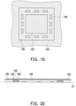
- FIG. 4A is a top view of a chip package of another embodiment of the invention.
- FIG. 4B is a cross-sectional view of a chip package of another embodiment of the invention.
- FIG. 5 is a cross-sectional view of a chip package of yet another embodiment of the invention.
- FIG. 6 is a cross-sectional view of a chip package of still yet another embodiment of the invention.
- FIG. 3A the structures of FIG. 1A and FIG. 2A in complete state are shown in FIG. 3A , i.e., the structure of FIG. 3A is partially shown in FIG. 1A and FIG. 2A .
- a supporting structure 120 and a carrier plate 110 are provided in the chip package process of the present embodiment.
- the supporting structure 120 is disposed on the carrier plate 110 .
- the supporting structure 120 has a plurality of openings 122 .
- the supporting structure 120 is one reticular structure, such as one reticular reinforced supporting member.
- the supporting structure having a plurality of openings and the carrier plate can alleviate warping occurring during the packaging process, and the effect is more significant for a fan-out wafer level package (FOWLP) or a fan-out panel level package (FOPLP) having a larger size.
- the structural strength of the chip package array 50 shown in FIG. 3C
- the production cost of the process can be lowered, such that the yield of the chip package 100 (shown in FIG. 1F and FIG. 2F ) can be increased.
- FIG. 3B the structures of FIG. 1B and FIG. 2B in complete state are shown in FIG. 3B , i.e., the structure of FIG. 3B is partially shown in FIG. 1B and FIG. 2B .
- a plurality of chips 130 is disposed on the carrier plate 110 , wherein the chips 130 are respectively located in a plurality of openings 122 of the supporting structure 120 .
- one chip 130 is disposed in one opening 122 , and the invention is not limited thereto.
- a plurality of chips can be disposed in one opening and disposed in the corresponding opening via a stacking method.
- the step of disposing the chips 130 on the carrier plate 110 further includes disposing a plurality of passive elements 140 on the carrier plate 110 that are located between the chips 130 and the supporting structure 120 .
- a plurality of the passive elements 140 can be disposed in each of the openings 122 to meet electrical requirements.
- an encapsulated material 150 such as molding compound, is formed to cover the supporting structure 120 and the chips 130 , wherein the supporting structure 120 and the chips 130 are located between the encapsulated material 150 and the carrier plate 110 , and the encapsulated material 150 is filled between the openings 122 and the chips 130 .
- the encapsulated material 150 is filled on the supporting structure 120 and completely covers the supporting structure 120 and the chips 130 such that each of the openings 122 in the supporting structure 120 is completely filled with the encapsulated material 150 to fix the supporting structure 120 and the chips 130 .
- the encapsulated material 150 also completely covers the passive elements 140 .
- the carrier plate 110 is removed. Since the encapsulated material 150 is completely filled in each of the openings 122 , the supporting structure 120 and the chips 130 are fixedly connected to each other via the encapsulated material 150 and do not separate. At this point, the supporting structure 120 , the chips 130 , the passive elements 140 , and the encapsulated material 150 form a first reference plane P 1 , i.e., the supporting structure 120 , the chips 130 , the passive elements 140 , and the encapsulated material 150 are coplanar.
- FIG. 3C the structures of FIG. 1E and FIG. 2E in complete state are shown in FIG. 3C , i.e., the structure of FIG. 3C is partially shown in FIG. 1E and FIG. 2E .
- the redistribution structure 160 is disposed on the supporting structure 120 and directly connected to the chips 130 , and via the disposition of the redistribution structure 160 , the signal originally disposed on the chips 130 is fanned-out outside the projection region of the chips 130 of the redistribution structure 160 , such that the flexibility of signal disposition of the chips 130 is increased.
- the conductive layer portion of the redistribution structure 160 can be directly electrically connected to a pad 130 a on the chips 130 without the addition of bumps.
- the redistribution structure 160 is disposed on the first reference plane P 1 and directly connected to the chips 130 .
- a plurality of solder balls 170 can be further disposed on the redistribution structure 160 , and the redistribution structure 160 is located between the chips 130 and the solder balls 170 .
- a chip package array 50 shown in FIG. 3C is completed, and the chip package array 50 contains a plurality of uncut chip packages 100 .
- the chip package array 50 is cut along a plurality of cutting lines L between the plurality of openings 122 to form a single chip package 100 as shown in FIG. 1F and FIG. 2F .
- each of the chip packages 100 formed by cutting the supporting structure 120 along the cutting lines L has a portion of the supporting structure 120 , and therefore the supporting structure 120 is one annular reinforced supporting member for a single chip package 100 and can increase the overall structural strength of the chip package 100 . More specifically, since the annular reinforced supporting member is formed by cutting along the cutting lines L, the reinforced supporting member is exposed at a side 102 of a single chip package 100 , and therefore better protection is provided to the peripheral region of the chip package 100 .
- the encapsulated material 150 and the redistribution structure 160 are also cut along the cutting lines L such that a portion of the encapsulated material 150 and a portion of the redistribution structure 160 are exposed at the side 102 of a single chip package 100 .
- the chip package array 50 includes a plurality of chip packages 100 , and the chip packages 100 are suitable for array arrangement to form the chip package array 50 as shown in FIG. 3C .
- Each of the chip packages 100 includes a redistribution structure 160 , a supporting structure 120 , a chip 130 , and an encapsulated material 150 .
- the supporting structure 120 is disposed on the redistribution structure 160 and has an opening 122 .
- the chip 130 is disposed on the redistribution structure 160 and located in the opening 122 .
- the encapsulated material 150 is located between the opening 122 and the chip 130 , wherein the encapsulated material 150 is filled between the opening 122 and the chip 130 , and the chip 130 and the supporting structure 120 are respectively directly connected to the redistribution structure 160 .
- the chip packages 100 are formed by cutting the chip package array 50 , and therefore the redistribution structure 160 , the supporting structure 120 , and the encapsulated material 150 are also cut and formed in each of the chip packages 100 .
- the supporting structure 120 is disposed in the peripheral region of each of the chip packages 100 of the chip package array 50 , warping occurring during the packaging process of the chip package array 50 can be alleviated, and the structural strength of the chip package array 50 can be increased and production cost of the process can be lowered, such that the yield of the chip packages 100 is increased. Moreover, the disposition of the supporting structure 120 can also improve the overall structural strength of each of the chip packages 100 .
- the chip packages 100 include a redistribution structure 160 , a supporting structure 120 , a chip 130 , and an encapsulated material 150 .
- the supporting structure 120 is disposed on the redistribution structure 160 and has an opening 122 .
- the chip 130 is disposed on the redistribution structure 160 and located in the opening 122 .
- the encapsulated material 150 is located between the opening 122 and the chip 130 , wherein the encapsulated material 150 is filled between the opening 122 and the chip 130 , and the chip 130 and the supporting structure 120 are respectively directly connected to the redistribution structure 160 .
- the chip packages 100 are formed by cutting the chip package array 50 (as shown in FIG. 3C ), and therefore the redistribution structure 160 , the supporting structure 120 , and the encapsulated material 150 are also cut and formed in each of the chip packages 100 . Since the supporting structure 120 is disposed in the peripheral region of the chip packages 100 , the overall structural strength of the chip packages 100 can be improved.
- a chip package 100 A of the present embodiment is similar to the chip package 100 of FIG. 1F and FIG. 2F , and the main difference between the two is the disposition of an encapsulated material 150 A.
- a portion of the encapsulated material 150 is removed to form the encapsulated material 150 A to expose the chips 130 .
- a portion of the encapsulated material 150 located on the supporting structure 120 and the chips 130 is removed and the encapsulated material 150 A located between the supporting structure 120 and the chips 130 is kept.
- a top surface 124 of the supporting structure 120 away from the redistribution structure 160 is coplanar with a first surface 132 of the chips 130 away from the redistribution structure 160 , i.e., both are located on a second reference plane P 2 .
- the chips 130 can be exposed outside the chip package 100 A to be in contact with a heat conductor such that the chip package 100 A has better heat dissipation.
- a chip package 100 B of the present embodiment is similar to the chip package 100 of FIG. 2F , and the main differences between the two are, for instance, the opening 122 of the present embodiment has an inner surface 126 , the inner surface 126 has at least one groove 128 , and the encapsulated material 150 is completely filled in the groove 128 .
- the overall structural strength of the chip package 100 B can be ensured by completely filling the encapsulated material 150 in the groove 128 .
- a portion of the encapsulated material 150 can be further removed to expose the chips 130 similarly as shown in FIG. 4A and FIG. 4B .
- a chip package 100 C of the present embodiment is similar to the chip package 100 of FIG. 2F , and the main differences between the two are, for instance, the opening 122 of the present embodiment has an inner surface 126 C, and the inner surface 126 C is inclined in a direction away from the chips 130 such that the encapsulated material 150 is extended above the inner surface 126 C.
- the supporting structure 120 can be covered via the extension of the encapsulated material 150 , such that the supporting structure 120 and the redistribution structure 160 are more tightly connected and are not readily fallen off.
- the overall structural strength of the chip package 100 C can be ensured by covering the inner surface 126 C of the encapsulated material 150 .
- a portion of the encapsulated material 150 can be further removed to expose the chips 130 similarly as shown in FIG. 4A and FIG. 4B .
- the disposition of the supporting structure can also improve the overall structural strength of each of the chip packages.
Abstract
Description
Claims (20)
Priority Applications (1)
| Application Number | Priority Date | Filing Date | Title |
|---|---|---|---|
| US15/636,644 US11227848B2 (en) | 2016-08-29 | 2017-06-29 | Chip package array, and chip package |
Applications Claiming Priority (4)
| Application Number | Priority Date | Filing Date | Title |
|---|---|---|---|
| US201662380960P | 2016-08-29 | 2016-08-29 | |
| TW106115539A TWI674647B (en) | 2016-08-29 | 2017-05-11 | Chip package array and chip package |
| TW106115539 | 2017-05-11 | ||
| US15/636,644 US11227848B2 (en) | 2016-08-29 | 2017-06-29 | Chip package array, and chip package |
Publications (2)
| Publication Number | Publication Date |
|---|---|
| US20180061788A1 US20180061788A1 (en) | 2018-03-01 |
| US11227848B2 true US11227848B2 (en) | 2022-01-18 |
Family
ID=79269558
Family Applications (1)
| Application Number | Title | Priority Date | Filing Date |
|---|---|---|---|
| US15/636,644 Active 2038-01-06 US11227848B2 (en) | 2016-08-29 | 2017-06-29 | Chip package array, and chip package |
Country Status (1)
| Country | Link |
|---|---|
| US (1) | US11227848B2 (en) |
Families Citing this family (4)
| Publication number | Priority date | Publication date | Assignee | Title |
|---|---|---|---|---|
| KR20180112463A (en) * | 2017-04-04 | 2018-10-12 | 에스케이하이닉스 주식회사 | Method of fabricating FOWLP |
| US11450620B2 (en) * | 2018-05-02 | 2022-09-20 | Intel Corporation | Innovative fan-out panel level package (FOPLP) warpage control |
| TWI768552B (en) * | 2020-11-20 | 2022-06-21 | 力成科技股份有限公司 | Stacked semiconductor package and packaging method thereof |
| CN112864027A (en) * | 2021-01-12 | 2021-05-28 | 浙江荷清柔性电子技术有限公司 | Fan-out type board level packaging method and structure thereof |
Citations (5)
| Publication number | Priority date | Publication date | Assignee | Title |
|---|---|---|---|---|
| US20100301474A1 (en) * | 2008-09-25 | 2010-12-02 | Wen-Kun Yang | Semiconductor Device Package Structure and Method for the Same |
| US20120153493A1 (en) * | 2010-12-17 | 2012-06-21 | Advanced Semiconductor Engineering, Inc. | Embedded component device and manufacturing methods thereof |
| US20150147849A1 (en) * | 2013-11-25 | 2015-05-28 | Samsung Electro-Mechanics Co., Ltd. | Method for manufacturing semiconductor package |
| US20160005628A1 (en) * | 2014-07-01 | 2016-01-07 | Freescal Semiconductor, Inc. | Wafer level packaging method and integrated electronic package |
| US20160336249A1 (en) * | 2015-05-11 | 2016-11-17 | Samsung Electro-Mechanics Co., Ltd. | Electronic component package and method of manufacturing the same |
-
2017
- 2017-06-29 US US15/636,644 patent/US11227848B2/en active Active
Patent Citations (5)
| Publication number | Priority date | Publication date | Assignee | Title |
|---|---|---|---|---|
| US20100301474A1 (en) * | 2008-09-25 | 2010-12-02 | Wen-Kun Yang | Semiconductor Device Package Structure and Method for the Same |
| US20120153493A1 (en) * | 2010-12-17 | 2012-06-21 | Advanced Semiconductor Engineering, Inc. | Embedded component device and manufacturing methods thereof |
| US20150147849A1 (en) * | 2013-11-25 | 2015-05-28 | Samsung Electro-Mechanics Co., Ltd. | Method for manufacturing semiconductor package |
| US20160005628A1 (en) * | 2014-07-01 | 2016-01-07 | Freescal Semiconductor, Inc. | Wafer level packaging method and integrated electronic package |
| US20160336249A1 (en) * | 2015-05-11 | 2016-11-17 | Samsung Electro-Mechanics Co., Ltd. | Electronic component package and method of manufacturing the same |
Also Published As
| Publication number | Publication date |
|---|---|
| US20180061788A1 (en) | 2018-03-01 |
Similar Documents
| Publication | Publication Date | Title |
|---|---|---|
| US11081371B2 (en) | Chip package process | |
| US10734367B2 (en) | Semiconductor package and method of fabricating the same | |
| KR101297015B1 (en) | Method of manufacturing fan-out semiconductor package using lead frame, semiconductor package thereof, and package on package thereof | |
| US7489044B2 (en) | Semiconductor package and fabrication method thereof | |
| US11227848B2 (en) | Chip package array, and chip package | |
| KR101368793B1 (en) | Semiconductor package and method of manufacturing the same | |
| US10332844B2 (en) | Manufacturing method of package structure | |
| KR20040053902A (en) | Multi chip package | |
| US9508657B2 (en) | Semiconductor package | |
| US10756077B2 (en) | Chip packaging method | |
| TWI719205B (en) | Chip package process | |
| TWI490960B (en) | Semiconductor package structure and manufacturing method thereof | |
| US11715714B2 (en) | Semiconductor devices and methods of manufacturing semiconductor devices | |
| US20220344175A1 (en) | Flip chip package unit and associated packaging method | |
| CN112185903A (en) | Electronic package and manufacturing method thereof | |
| TW201721813A (en) | Semiconductor device and manufacturing method of the same | |
| US20080185698A1 (en) | Semiconductor package structure and carrier structure | |
| US11227814B2 (en) | Three-dimensional semiconductor package with partially overlapping chips and manufacturing method thereof | |
| US11417581B2 (en) | Package structure | |
| US9905491B1 (en) | Interposer substrate designs for semiconductor packages | |
| US11469219B1 (en) | Dual die semiconductor package and manufacturing method thereof | |
| US20080157304A1 (en) | Chip package structure | |
| KR101209472B1 (en) | Lead frame for fabricating semiconductor package and Method for fabricating semiconductor package using the same | |
| US20160163629A1 (en) | Semiconductor package and method of fabricating the same | |
| KR101538546B1 (en) | Fabricating Method Of Semiconductor Device and Semiconduntor Device Fabricated Using The Same |
Legal Events
| Date | Code | Title | Description |
|---|---|---|---|
| AS | Assignment |
Owner name: VIA ALLIANCE SEMICONDUCTOR CO., LTD., CHINA Free format text: ASSIGNMENT OF ASSIGNORS INTEREST;ASSIGNORS:CHANG, WEN-YUAN;CHEN, WEI-CHENG;LU, HSUEH-CHUNG SHELTON;SIGNING DATES FROM 20170221 TO 20170301;REEL/FRAME:042855/0464 |
|
| STPP | Information on status: patent application and granting procedure in general |
Free format text: DOCKETED NEW CASE - READY FOR EXAMINATION |
|
| STPP | Information on status: patent application and granting procedure in general |
Free format text: NON FINAL ACTION MAILED |
|
| STPP | Information on status: patent application and granting procedure in general |
Free format text: RESPONSE TO NON-FINAL OFFICE ACTION ENTERED AND FORWARDED TO EXAMINER |
|
| STPP | Information on status: patent application and granting procedure in general |
Free format text: FINAL REJECTION MAILED |
|
| STPP | Information on status: patent application and granting procedure in general |
Free format text: DOCKETED NEW CASE - READY FOR EXAMINATION |
|
| STPP | Information on status: patent application and granting procedure in general |
Free format text: NON FINAL ACTION MAILED |
|
| STPP | Information on status: patent application and granting procedure in general |
Free format text: RESPONSE TO NON-FINAL OFFICE ACTION ENTERED AND FORWARDED TO EXAMINER |
|
| STPP | Information on status: patent application and granting procedure in general |
Free format text: AWAITING TC RESP., ISSUE FEE NOT PAID |
|
| STPP | Information on status: patent application and granting procedure in general |
Free format text: PUBLICATIONS -- ISSUE FEE PAYMENT VERIFIED |
|
| STCF | Information on status: patent grant |
Free format text: PATENTED CASE |