US11226527B2 - Display device - Google Patents

Display device Download PDF

Info

Publication number
US11226527B2
US11226527B2 US16/802,442 US202016802442A US11226527B2 US 11226527 B2 US11226527 B2 US 11226527B2 US 202016802442 A US202016802442 A US 202016802442A US 11226527 B2 US11226527 B2 US 11226527B2
Authority
US
United States
Prior art keywords
data line
line
disposed
region
pixel
Prior art date
Legal status (The legal status is an assumption and is not a legal conclusion. Google has not performed a legal analysis and makes no representation as to the accuracy of the status listed.)
Active
Application number
US16/802,442
Other versions
US20200348571A1 (en
Inventor
Gwon-Heon Ryu
Kwi Hyun Kim
Kook Hyun CHOI
Woo Gun Kang
Kyung Won Park
Jin Su Lee
Current Assignee (The listed assignees may be inaccurate. Google has not performed a legal analysis and makes no representation or warranty as to the accuracy of the list.)
Samsung Display Co Ltd
Original Assignee
Samsung Display Co Ltd
Priority date (The priority date is an assumption and is not a legal conclusion. Google has not performed a legal analysis and makes no representation as to the accuracy of the date listed.)
Filing date
Publication date
Application filed by Samsung Display Co Ltd filed Critical Samsung Display Co Ltd
Assigned to SAMSUNG DISPLAY CO., LTD. reassignment SAMSUNG DISPLAY CO., LTD. ASSIGNMENT OF ASSIGNORS INTEREST (SEE DOCUMENT FOR DETAILS). Assignors: CHOI, KOOK HYUN, KANG, Woo Gun, KIM, KWI HYUN, LEE, JIN SU, PARK, KYUNG WON, Ryu, Gwon-Heon
Publication of US20200348571A1 publication Critical patent/US20200348571A1/en
Priority to US17/543,725 priority Critical patent/US11762251B2/en
Application granted granted Critical
Publication of US11226527B2 publication Critical patent/US11226527B2/en
Active legal-status Critical Current
Anticipated expiration legal-status Critical

Links

Images

Classifications

    • GPHYSICS
    • G02OPTICS
    • G02FOPTICAL DEVICES OR ARRANGEMENTS FOR THE CONTROL OF LIGHT BY MODIFICATION OF THE OPTICAL PROPERTIES OF THE MEDIA OF THE ELEMENTS INVOLVED THEREIN; NON-LINEAR OPTICS; FREQUENCY-CHANGING OF LIGHT; OPTICAL LOGIC ELEMENTS; OPTICAL ANALOGUE/DIGITAL CONVERTERS
    • G02F1/00Devices or arrangements for the control of the intensity, colour, phase, polarisation or direction of light arriving from an independent light source, e.g. switching, gating or modulating; Non-linear optics
    • G02F1/01Devices or arrangements for the control of the intensity, colour, phase, polarisation or direction of light arriving from an independent light source, e.g. switching, gating or modulating; Non-linear optics for the control of the intensity, phase, polarisation or colour 
    • G02F1/13Devices or arrangements for the control of the intensity, colour, phase, polarisation or direction of light arriving from an independent light source, e.g. switching, gating or modulating; Non-linear optics for the control of the intensity, phase, polarisation or colour  based on liquid crystals, e.g. single liquid crystal display cells
    • G02F1/133Constructional arrangements; Operation of liquid crystal cells; Circuit arrangements
    • G02F1/1333Constructional arrangements; Manufacturing methods
    • G02F1/1343Electrodes
    • G02F1/134309Electrodes characterised by their geometrical arrangement
    • GPHYSICS
    • G02OPTICS
    • G02FOPTICAL DEVICES OR ARRANGEMENTS FOR THE CONTROL OF LIGHT BY MODIFICATION OF THE OPTICAL PROPERTIES OF THE MEDIA OF THE ELEMENTS INVOLVED THEREIN; NON-LINEAR OPTICS; FREQUENCY-CHANGING OF LIGHT; OPTICAL LOGIC ELEMENTS; OPTICAL ANALOGUE/DIGITAL CONVERTERS
    • G02F1/00Devices or arrangements for the control of the intensity, colour, phase, polarisation or direction of light arriving from an independent light source, e.g. switching, gating or modulating; Non-linear optics
    • G02F1/01Devices or arrangements for the control of the intensity, colour, phase, polarisation or direction of light arriving from an independent light source, e.g. switching, gating or modulating; Non-linear optics for the control of the intensity, phase, polarisation or colour 
    • G02F1/13Devices or arrangements for the control of the intensity, colour, phase, polarisation or direction of light arriving from an independent light source, e.g. switching, gating or modulating; Non-linear optics for the control of the intensity, phase, polarisation or colour  based on liquid crystals, e.g. single liquid crystal display cells
    • G02F1/133Constructional arrangements; Operation of liquid crystal cells; Circuit arrangements
    • G02F1/1333Constructional arrangements; Manufacturing methods
    • G02F1/1343Electrodes
    • G02F1/134309Electrodes characterised by their geometrical arrangement
    • G02F1/134345Subdivided pixels, e.g. for grey scale or redundancy
    • G02F1/134354Subdivided pixels, e.g. for grey scale or redundancy the sub-pixels being capacitively coupled
    • GPHYSICS
    • G02OPTICS
    • G02FOPTICAL DEVICES OR ARRANGEMENTS FOR THE CONTROL OF LIGHT BY MODIFICATION OF THE OPTICAL PROPERTIES OF THE MEDIA OF THE ELEMENTS INVOLVED THEREIN; NON-LINEAR OPTICS; FREQUENCY-CHANGING OF LIGHT; OPTICAL LOGIC ELEMENTS; OPTICAL ANALOGUE/DIGITAL CONVERTERS
    • G02F1/00Devices or arrangements for the control of the intensity, colour, phase, polarisation or direction of light arriving from an independent light source, e.g. switching, gating or modulating; Non-linear optics
    • G02F1/01Devices or arrangements for the control of the intensity, colour, phase, polarisation or direction of light arriving from an independent light source, e.g. switching, gating or modulating; Non-linear optics for the control of the intensity, phase, polarisation or colour 
    • G02F1/13Devices or arrangements for the control of the intensity, colour, phase, polarisation or direction of light arriving from an independent light source, e.g. switching, gating or modulating; Non-linear optics for the control of the intensity, phase, polarisation or colour  based on liquid crystals, e.g. single liquid crystal display cells
    • G02F1/133Constructional arrangements; Operation of liquid crystal cells; Circuit arrangements
    • G02F1/136Liquid crystal cells structurally associated with a semi-conducting layer or substrate, e.g. cells forming part of an integrated circuit
    • G02F1/1362Active matrix addressed cells
    • G02F1/136209Light shielding layers, e.g. black matrix, incorporated in the active matrix substrate, e.g. structurally associated with the switching element
    • GPHYSICS
    • G02OPTICS
    • G02FOPTICAL DEVICES OR ARRANGEMENTS FOR THE CONTROL OF LIGHT BY MODIFICATION OF THE OPTICAL PROPERTIES OF THE MEDIA OF THE ELEMENTS INVOLVED THEREIN; NON-LINEAR OPTICS; FREQUENCY-CHANGING OF LIGHT; OPTICAL LOGIC ELEMENTS; OPTICAL ANALOGUE/DIGITAL CONVERTERS
    • G02F1/00Devices or arrangements for the control of the intensity, colour, phase, polarisation or direction of light arriving from an independent light source, e.g. switching, gating or modulating; Non-linear optics
    • G02F1/01Devices or arrangements for the control of the intensity, colour, phase, polarisation or direction of light arriving from an independent light source, e.g. switching, gating or modulating; Non-linear optics for the control of the intensity, phase, polarisation or colour 
    • G02F1/13Devices or arrangements for the control of the intensity, colour, phase, polarisation or direction of light arriving from an independent light source, e.g. switching, gating or modulating; Non-linear optics for the control of the intensity, phase, polarisation or colour  based on liquid crystals, e.g. single liquid crystal display cells
    • G02F1/133Constructional arrangements; Operation of liquid crystal cells; Circuit arrangements
    • G02F1/136Liquid crystal cells structurally associated with a semi-conducting layer or substrate, e.g. cells forming part of an integrated circuit
    • G02F1/1362Active matrix addressed cells
    • G02F1/136213Storage capacitors associated with the pixel electrode
    • GPHYSICS
    • G02OPTICS
    • G02FOPTICAL DEVICES OR ARRANGEMENTS FOR THE CONTROL OF LIGHT BY MODIFICATION OF THE OPTICAL PROPERTIES OF THE MEDIA OF THE ELEMENTS INVOLVED THEREIN; NON-LINEAR OPTICS; FREQUENCY-CHANGING OF LIGHT; OPTICAL LOGIC ELEMENTS; OPTICAL ANALOGUE/DIGITAL CONVERTERS
    • G02F1/00Devices or arrangements for the control of the intensity, colour, phase, polarisation or direction of light arriving from an independent light source, e.g. switching, gating or modulating; Non-linear optics
    • G02F1/01Devices or arrangements for the control of the intensity, colour, phase, polarisation or direction of light arriving from an independent light source, e.g. switching, gating or modulating; Non-linear optics for the control of the intensity, phase, polarisation or colour 
    • G02F1/13Devices or arrangements for the control of the intensity, colour, phase, polarisation or direction of light arriving from an independent light source, e.g. switching, gating or modulating; Non-linear optics for the control of the intensity, phase, polarisation or colour  based on liquid crystals, e.g. single liquid crystal display cells
    • G02F1/133Constructional arrangements; Operation of liquid crystal cells; Circuit arrangements
    • G02F1/136Liquid crystal cells structurally associated with a semi-conducting layer or substrate, e.g. cells forming part of an integrated circuit
    • G02F1/1362Active matrix addressed cells
    • G02F1/136227Through-hole connection of the pixel electrode to the active element through an insulation layer
    • GPHYSICS
    • G02OPTICS
    • G02FOPTICAL DEVICES OR ARRANGEMENTS FOR THE CONTROL OF LIGHT BY MODIFICATION OF THE OPTICAL PROPERTIES OF THE MEDIA OF THE ELEMENTS INVOLVED THEREIN; NON-LINEAR OPTICS; FREQUENCY-CHANGING OF LIGHT; OPTICAL LOGIC ELEMENTS; OPTICAL ANALOGUE/DIGITAL CONVERTERS
    • G02F1/00Devices or arrangements for the control of the intensity, colour, phase, polarisation or direction of light arriving from an independent light source, e.g. switching, gating or modulating; Non-linear optics
    • G02F1/01Devices or arrangements for the control of the intensity, colour, phase, polarisation or direction of light arriving from an independent light source, e.g. switching, gating or modulating; Non-linear optics for the control of the intensity, phase, polarisation or colour 
    • G02F1/13Devices or arrangements for the control of the intensity, colour, phase, polarisation or direction of light arriving from an independent light source, e.g. switching, gating or modulating; Non-linear optics for the control of the intensity, phase, polarisation or colour  based on liquid crystals, e.g. single liquid crystal display cells
    • G02F1/133Constructional arrangements; Operation of liquid crystal cells; Circuit arrangements
    • G02F1/136Liquid crystal cells structurally associated with a semi-conducting layer or substrate, e.g. cells forming part of an integrated circuit
    • G02F1/1362Active matrix addressed cells
    • G02F1/136286Wiring, e.g. gate line, drain line
    • GPHYSICS
    • G09EDUCATION; CRYPTOGRAPHY; DISPLAY; ADVERTISING; SEALS
    • G09GARRANGEMENTS OR CIRCUITS FOR CONTROL OF INDICATING DEVICES USING STATIC MEANS TO PRESENT VARIABLE INFORMATION
    • G09G3/00Control arrangements or circuits, of interest only in connection with visual indicators other than cathode-ray tubes
    • G09G3/20Control arrangements or circuits, of interest only in connection with visual indicators other than cathode-ray tubes for presentation of an assembly of a number of characters, e.g. a page, by composing the assembly by combination of individual elements arranged in a matrix no fixed position being assigned to or needed to be assigned to the individual characters or partial characters
    • G09G3/34Control arrangements or circuits, of interest only in connection with visual indicators other than cathode-ray tubes for presentation of an assembly of a number of characters, e.g. a page, by composing the assembly by combination of individual elements arranged in a matrix no fixed position being assigned to or needed to be assigned to the individual characters or partial characters by control of light from an independent source
    • G09G3/36Control arrangements or circuits, of interest only in connection with visual indicators other than cathode-ray tubes for presentation of an assembly of a number of characters, e.g. a page, by composing the assembly by combination of individual elements arranged in a matrix no fixed position being assigned to or needed to be assigned to the individual characters or partial characters by control of light from an independent source using liquid crystals
    • G09G3/3611Control of matrices with row and column drivers
    • G09G3/3648Control of matrices with row and column drivers using an active matrix
    • GPHYSICS
    • G02OPTICS
    • G02FOPTICAL DEVICES OR ARRANGEMENTS FOR THE CONTROL OF LIGHT BY MODIFICATION OF THE OPTICAL PROPERTIES OF THE MEDIA OF THE ELEMENTS INVOLVED THEREIN; NON-LINEAR OPTICS; FREQUENCY-CHANGING OF LIGHT; OPTICAL LOGIC ELEMENTS; OPTICAL ANALOGUE/DIGITAL CONVERTERS
    • G02F1/00Devices or arrangements for the control of the intensity, colour, phase, polarisation or direction of light arriving from an independent light source, e.g. switching, gating or modulating; Non-linear optics
    • G02F1/01Devices or arrangements for the control of the intensity, colour, phase, polarisation or direction of light arriving from an independent light source, e.g. switching, gating or modulating; Non-linear optics for the control of the intensity, phase, polarisation or colour 
    • G02F1/13Devices or arrangements for the control of the intensity, colour, phase, polarisation or direction of light arriving from an independent light source, e.g. switching, gating or modulating; Non-linear optics for the control of the intensity, phase, polarisation or colour  based on liquid crystals, e.g. single liquid crystal display cells
    • G02F1/133Constructional arrangements; Operation of liquid crystal cells; Circuit arrangements
    • G02F1/1333Constructional arrangements; Manufacturing methods
    • G02F1/1337Surface-induced orientation of the liquid crystal molecules, e.g. by alignment layers
    • G02F1/133707Structures for producing distorted electric fields, e.g. bumps, protrusions, recesses, slits in pixel electrodes
    • GPHYSICS
    • G02OPTICS
    • G02FOPTICAL DEVICES OR ARRANGEMENTS FOR THE CONTROL OF LIGHT BY MODIFICATION OF THE OPTICAL PROPERTIES OF THE MEDIA OF THE ELEMENTS INVOLVED THEREIN; NON-LINEAR OPTICS; FREQUENCY-CHANGING OF LIGHT; OPTICAL LOGIC ELEMENTS; OPTICAL ANALOGUE/DIGITAL CONVERTERS
    • G02F1/00Devices or arrangements for the control of the intensity, colour, phase, polarisation or direction of light arriving from an independent light source, e.g. switching, gating or modulating; Non-linear optics
    • G02F1/01Devices or arrangements for the control of the intensity, colour, phase, polarisation or direction of light arriving from an independent light source, e.g. switching, gating or modulating; Non-linear optics for the control of the intensity, phase, polarisation or colour 
    • G02F1/13Devices or arrangements for the control of the intensity, colour, phase, polarisation or direction of light arriving from an independent light source, e.g. switching, gating or modulating; Non-linear optics for the control of the intensity, phase, polarisation or colour  based on liquid crystals, e.g. single liquid crystal display cells
    • G02F1/133Constructional arrangements; Operation of liquid crystal cells; Circuit arrangements
    • G02F1/1333Constructional arrangements; Manufacturing methods
    • G02F1/1343Electrodes
    • G02F1/134309Electrodes characterised by their geometrical arrangement
    • G02F1/134345Subdivided pixels, e.g. for grey scale or redundancy
    • GPHYSICS
    • G02OPTICS
    • G02FOPTICAL DEVICES OR ARRANGEMENTS FOR THE CONTROL OF LIGHT BY MODIFICATION OF THE OPTICAL PROPERTIES OF THE MEDIA OF THE ELEMENTS INVOLVED THEREIN; NON-LINEAR OPTICS; FREQUENCY-CHANGING OF LIGHT; OPTICAL LOGIC ELEMENTS; OPTICAL ANALOGUE/DIGITAL CONVERTERS
    • G02F2201/00Constructional arrangements not provided for in groups G02F1/00 - G02F7/00
    • G02F2201/12Constructional arrangements not provided for in groups G02F1/00 - G02F7/00 electrode
    • G02F2201/123Constructional arrangements not provided for in groups G02F1/00 - G02F7/00 electrode pixel
    • GPHYSICS
    • G02OPTICS
    • G02FOPTICAL DEVICES OR ARRANGEMENTS FOR THE CONTROL OF LIGHT BY MODIFICATION OF THE OPTICAL PROPERTIES OF THE MEDIA OF THE ELEMENTS INVOLVED THEREIN; NON-LINEAR OPTICS; FREQUENCY-CHANGING OF LIGHT; OPTICAL LOGIC ELEMENTS; OPTICAL ANALOGUE/DIGITAL CONVERTERS
    • G02F2203/00Function characteristic
    • G02F2203/30Gray scale
    • GPHYSICS
    • G09EDUCATION; CRYPTOGRAPHY; DISPLAY; ADVERTISING; SEALS
    • G09GARRANGEMENTS OR CIRCUITS FOR CONTROL OF INDICATING DEVICES USING STATIC MEANS TO PRESENT VARIABLE INFORMATION
    • G09G2300/00Aspects of the constitution of display devices
    • G09G2300/04Structural and physical details of display devices
    • G09G2300/0421Structural details of the set of electrodes
    • G09G2300/0426Layout of electrodes and connections
    • GPHYSICS
    • G09EDUCATION; CRYPTOGRAPHY; DISPLAY; ADVERTISING; SEALS
    • G09GARRANGEMENTS OR CIRCUITS FOR CONTROL OF INDICATING DEVICES USING STATIC MEANS TO PRESENT VARIABLE INFORMATION
    • G09G2320/00Control of display operating conditions
    • G09G2320/02Improving the quality of display appearance
    • G09G2320/0223Compensation for problems related to R-C delay and attenuation in electrodes of matrix panels, e.g. in gate electrodes or on-substrate video signal electrodes
    • GPHYSICS
    • G09EDUCATION; CRYPTOGRAPHY; DISPLAY; ADVERTISING; SEALS
    • G09GARRANGEMENTS OR CIRCUITS FOR CONTROL OF INDICATING DEVICES USING STATIC MEANS TO PRESENT VARIABLE INFORMATION
    • G09G2320/00Control of display operating conditions
    • G09G2320/02Improving the quality of display appearance
    • G09G2320/0233Improving the luminance or brightness uniformity across the screen

Definitions

  • the present disclosure relates to a display device, and in detail, relates to a display device for differentiating a capacitance for each region of the display device.
  • a liquid crystal display is a flat panel display that is widely used and includes two display panel sheets in which field generating electrodes such as pixel electrodes and common electrodes are formed, and a liquid crystal layer interposed between the display panels.
  • a voltage is applied to the field generating electrodes to generate an electric field in the liquid crystal layer, which determines the direction of liquid crystal molecules of the liquid crystal layer, and an image is displayed by controlling the polarization of incident light.
  • the liquid crystal display also includes a switching element connected to each pixel electrode, and a plurality of signal lines such as a gate line and a data line for applying a voltage to the pixel electrode by controlling the switching element.
  • Exemplary embodiments provide a display device capable of compensate a luminance difference by a data voltage.
  • a display device includes: a substrate including a first region and a second region; and a plurality of pixels disposed on the substrate, wherein the plurality of pixels each include a first data line and a second data line overlapping a pixel electrode, a first capacitance between the first data line and the pixel electrode is smaller than a second capacitance between the second data line and the pixel electrode in a pixel disposed in the first region, and the first capacitance between the first data line and the pixel electrode is larger than the second capacitance between the second data line and the pixel electrode in a pixel disposed in the second region.
  • the display panel may be scanned in a direction from the first region to the second region.
  • the plurality of pixels may each include: a gate line disposed on the substrate; a data line disposed to be insulated from the gate line; the pixel electrode disposed to overlap the first data line and the second data line; and a pixel electrode protrusion connected to the pixel electrode, wherein the data line may include the first data line and the second data line, and the pixel disposed in the first region may include a second pixel electrode protrusion overlapping the second data line.
  • An area of the first pixel electrode protrusion overlapping the first data line in the pixel disposed in the second region may be wider than an area of the first pixel electrode protrusion overlapping the first data line of the pixel disposed in the first region.
  • the first data line may be electrically connected to the pixel electrode of the pixel, and the second data line may not be electrically connected to the pixel electrode that is electrically connected to the first data line.
  • the pixel may include a display area and a light blocking area, and in the light blocking area of the pixel disposed in the first region, a width of the first data line may be narrower than a width of the second data line.
  • a width of the first data line may be wider than a width of the second data line.
  • a plurality of semiconductor layers disposed between the gate line and the data line may be further included, and the plurality of semiconductor layers may each include a dummy semiconductor layer disposed at a region where the gate line and the data line cross each other.
  • the gate line may include a first gate line and a second gate line parallel to each other, and a gate electrode disposed between the first gate line and the second gate line, and a part of the plurality of semiconductor layers, may be disposed to overlap the gate electrode so as to configure a transistor.
  • the first data line and the second data line may be curved at one edge of the pixel electrode, and a curved length of the second data line may be longer than a curved length of the first data line.
  • a storage electrode line disposed on the same layer as the gate line may be further included, the storage electrode line may include a first storage electrode line, a second storage electrode line, and a third storage electrode line, the first storage electrode line may be disposed to be adjacent to one edge of the pixel electrode, the third storage electrode line may be disposed to be adjacent to another edge of the pixel electrode, and the second storage electrode line may be disposed to overlap the center of the pixel electrode.
  • the first data line may be disposed between the first storage electrode line and the second storage electrode line
  • the second data line may be disposed between the second storage electrode line and the third storage electrode line.
  • a display device includes: a substrate including a first region and a second region; and a plurality of pixels disposed on the substrate, wherein the plurality of pixels each include a first data line and a second data line overlapping a pixel electrode, in a pixel disposed in the first region, a first capacitance between the first data line and the pixel electrode is smaller than a second capacitance between the second data line and the pixel electrode, and a difference between the first capacitance and the second capacitance in the first region decreases stepwise closer to the second region.
  • a first capacitance between the first data line and the pixel electrode may be larger than a second capacitance between the second data line and the pixel electrode, and in the second region, a difference between the first capacitance and the second capacitance may increase stepwise farther away from the first region.
  • the first capacitance and the second capacitance may be equal in the center region of the substrate.
  • the plurality of pixels may each include: a gate line disposed on the substrate; a data line disposed to be insulated from the gate line; a pixel electrode disposed to overlap the first data line and the second data line; and a pixel electrode protrusion connected to the pixel electrode, wherein the data line may include the first data line and the second data line, the pixel disposed in the first region may include a second pixel electrode protrusion overlapping the second data line, and the area of the first pixel electrode protrusion overlapping the first data line in the pixel disposed in the second region may be larger than the area of the first pixel electrode protrusion overlapping the first data line of the pixel disposed in the first region.
  • the pixel may include a display area and a light blocking area, and in the pixel disposed in the first region, the width of the first data line may be narrower than the width of the second data line in the light blocking area, while in the pixel disposed in the second region, the width of the first data line may be wider than the width of the second data line in the light blocking area.
  • the first data line may be electrically connected to the pixel electrode of the pixel, and the second data line may not be electrically connected to the pixel electrode that is electrically connected to the first data line.
  • a display device includes: a substrate including a first region and a second region; and a plurality of pixels disposed on the substrate, wherein the pixels include a first data line and a second data line overlapping a pixel electrode, a pixel disposed in the first region includes a second pixel electrode protrusion overlapping the second data line, and an area of the first pixel electrode protrusion overlapping the first data line in the pixel disposed in the second region is larger than an area of the first pixel electrode protrusion overlapping the first data line of the pixel disposed in the first region.
  • a display device includes: a substrate including a first region and a second region; and a plurality of pixels disposed on the substrate, wherein the plurality of pixels each include a first data line and a second data line overlapping a pixel electrode, the pixels include a display area and a light blocking area, in the pixel disposed in the first region, a width of the first data line is narrower than a width of the second data line in the light blocking area, and in a pixel disposed in the second region, a width of the first data line is wider than a width of the second data line in the light blocking area.
  • a display device capable of compensating a luminance difference by a data voltage is provided.
  • FIG. 1 is a view schematically showing a display device according to an embodiment of the present inventive concept.
  • FIG. 2 is a layout view of one pixel disposed in a first region A 1 .
  • FIG. 3A is a cross-sectional view of a display device of FIG. 2 taken along a line IIIa-IIIa′.
  • FIG. 3B is a cross-sectional view of a display device of FIG. 2 taken along a line IIIb-IIIb′.
  • FIG. 4 is a layout view of one pixel disposed in a second region A 2 .
  • FIG. 5 shows various causes that affect a luminance and results in a display device.
  • FIGS. 6A and 6B are views for measuring a luminance of a display device when displaying an image without a white box.
  • FIG. 6A shows a measuring position
  • FIG. 6B is an image for measuring a luminance at a measuring position.
  • FIGS. 7A, 7B, 7C, and 7D are views for measuring a luminance of a display device when displaying an image including a white box.
  • FIG. 7A shows a measuring position
  • FIG. 7B is an image for measuring a luminance at a measuring position.
  • FIG. 7C shows a luminance for each position for the same cross-section as in FIG. 3B .
  • FIG. 7D shows a reason that a luminance is high near a first data line and a luminance is low near a second data line.
  • FIGS. 8A, 8B, and 8C are views showing a luminance in upper and lower regions of a white box of a display device when a self-capacitance is larger than a neighboring-capacitance.
  • FIG. 8A is a view showing a brightness in an upper end and a lower end of a white box when a self-capacitance is larger than a neighboring-capacitance.
  • FIG. 8B is a view showing a voltage behavior in an upper end of a white box.
  • FIG. 8C is a view showing a voltage behavior in a lower end of a white box.
  • FIGS. 9A, 9B, and 9C are views showing a luminance in upper and lower regions of a white box of a display device when a self-capacitance is smaller than a neighboring-capacitance.
  • FIG. 9A is a view showing a brightness in an upper end and a lower end of a white box when a self-capacitance is smaller than a neighboring-capacitance.
  • FIG. 9 B is a view showing a voltage behavior in an upper end of a white box.
  • FIG. 9C is a view showing a voltage behavior in a lower end of a white box.
  • FIG. 10 is a top plan view of a pixel disposed in a first region A 1 according to another embodiment.
  • FIG. 11 is a top plan view of a pixel disposed in a second region A 2 according to another embodiment.
  • FIG. 12 is a view showing a display device according to another embodiment of the present inventive concept.
  • the phrase “on a plane” means viewing a target portion from the top
  • the phrase “on a cross-section” means viewing a cross-section formed by vertically cutting a target portion from the side.
  • FIG. 1 is a view schematically showing a display device 1000 according to an embodiment of the present inventive concept.
  • the display device 1000 according to an embodiment of the present inventive concept includes a first region A 1 and a second region A 2 .
  • the first region A 1 and the second region A 2 are disposed at opposite sides with respect to a center in a second direction DR 2 of the display device 1000 .
  • a scan is performed in a direction from the first region A 1 to the second region A 2 .
  • capacitances Cdp between a data line and a pixel electrode in the first region A 1 and the second region A 2 are different from each other.
  • the pixel electrode overlaps two data lines.
  • one data line is the data line connected to a corresponding pixel (hereinafter, a first data line)
  • the other data line is the data line connected to a neighboring pixel (hereinafter, a second data line).
  • the capacitance between the first data line and the pixel electrode (hereinafter, a self-capacitance Cdp 1 ) is smaller than the capacitance between the second data line and the pixel electrode (hereinafter, a neighboring-capacitance Cdp 2 ).
  • the self-capacitance Cdp 1 is larger than the neighboring-capacitance Cdp 2 .
  • the luminance deviation due to the data voltage may be compensated. Detailed effects are described in detail later.
  • the meaning of the pixel includes the area occupied by one transistor and the pixel electrode 2 connected thereto, and FIG. 2 shows one pixel.
  • FIG. 2 is a layout view of one pixel disposed in a first region A 1 .
  • FIG. 3A is a cross-sectional view of a display device of FIG. 2 taken along a line IIIa-IIIa′.
  • FIG. 3B is a cross-sectional view of a display device of FIG. 2 taken along a line IIIb-IIIb′.
  • a plurality of gate lines 121 disposed on a first substrate 110 made of transparent glass or plastic are included.
  • the gate lines 121 transmit a gate signal and extend in a first direction DR 1 .
  • Each gate line 121 includes a first gate line 121 a and a second gate line 121 b that are separated from each other, and a gate electrode 124 connecting the first gate line 121 a and the second gate line 121 b.
  • a storage electrode line 129 may be disposed on the same layer as the gate line 121 .
  • the storage electrode line 129 includes a first storage electrode line 129 a , a second storage electrode line 129 b , and a third storage electrode line 129 c extending in the second direction DR 2 , and the first storage electrode line 129 a , the second storage electrode line 129 b , and the third storage electrode line 129 c are connected to a transverse storage electrode line 129 d extending parallel to the first direction DR 1 .
  • the second storage electrode line 129 b may include two parts that are separated from each other, and the second storage electrode line 129 b that is not connected to the transverse storage electrode line 129 d may be disposed with an island shape.
  • a gate insulating layer 140 made of an insulating material such as a silicon oxide or a silicon nitride is disposed on the gate line 121 and the storage electrode line 129 .
  • the gate insulating layer 140 may have a multilayered structure including at least two insulating layers having different physical properties.
  • a plurality of semiconductor layers 154 are disposed on the gate insulating layer 140 .
  • the semiconductor layer 154 may be disposed overlapping the gate electrode 124 .
  • dummy semiconductor layers 155 disposed on the same layer as the semiconductor layer 154 may be disposed at a position where the gate line 121 and the data line 171 are crossed and a position where the storage electrode line 129 and the data line 171 are crossed. These dummy semiconductor layers 155 smooth a step at the region where the wires are crossed. However, the dummy semiconductor layer 155 does not constitute a transistor or the like.
  • a plurality of data lines 171 , a plurality of source electrodes 173 connected to the data lines 171 , and a plurality of drain electrodes 175 are disposed on the semiconductor layer 154 and the gate insulating layer 140 .
  • the data line 171 extends in the second direction DR 2 , thereby crossing the gate line 121 .
  • the data line 171 includes a first data line 171 a and a second data line 171 b .
  • the first data line 171 a and the second data line 171 b overlap the pixel electrode 191 , and are disposed without overlapping the storage electrode line 129 .
  • first data line 171 a may be disposed between the first storage electrode line 129 a and the second storage electrode line 129 b .
  • second data line 171 b may be disposed between the second storage electrode line 129 b and the third storage electrode line 129 c.
  • the first data line 171 a each constitutes a respective transistor of the overlapping pixels.
  • the second data line 171 b constitutes the transistors of other pixels (not shown) neighboring in the second direction. That is, in the present embodiment, two data lines overlap one pixel electrode 191 , but only one data line 171 a is electrically connected to the pixel electrode 191 and the other data line 171 b is electrically connected to the pixel electrode neighboring thereto.
  • the second data line 171 b may be disposed to be curved and/or bent near the edge of the pixel electrode 191 in the second direction DR 2 .
  • the first data line 171 a may be also disposed to be curved near the edge of the pixel electrode 191 in the second direction DR 2 .
  • the curved length 312 b of the second data line 171 b may be longer than the curved length 312 a of the first data line 171 a (e.g., the length of the bent portion of the second data line 171 b may be longer than the bent portion of the first data line 171 a ).
  • a portion of the first data line 171 a constitutes the source electrode 173 .
  • the source electrode 173 extends from the data line 171 and overlaps the gate electrode 124 , and may have an approximate U-shape.
  • the drain electrode 175 is separated from the data line 171 , and extends from the center of the U-shape of the source electrode 173 toward the top.
  • One gate electrode 124 , one source electrode 173 , and one drain electrode 175 form one thin film transistor (TFT) together with the semiconductor layer 154 , and the channel region of the thin film transistor is formed in the semiconductor layer 154 between the source electrode 173 and the drain electrodes 175 .
  • TFT thin film transistor
  • the color filters may include a red color filter, a green color filter, and a blue color filter. Each color filter may be located in the region corresponding to one pixel electrode 191 .
  • the insulating layer 180 may be made of an inorganic insulator such as a silicon nitride or a silicon oxide, an organic insulator, or a low dielectric constant insulator.
  • the insulating layer 180 and the color filter 230 include a contact hole 181 overlapping the drain electrode 175 .
  • the pixel electrode 191 is physically and electrically connected to the drain electrode 175 through the contact hole 181 , thereby receiving the data voltage from the drain electrode 175 .
  • the pixel electrode 191 may include a transparent conductor such as ITO or IZO.
  • the pixel electrode includes a transverse stem part 192 extending in the first direction DR 1 , and a longitudinal stem part 193 crossing the transverse stem part and extending in the second direction DR 2 . Fine branches 199 extend from each stem part.
  • the pixel electrode 191 overlaps both the first storage electrode line 129 a and the third storage electrode line 129 c , and includes an outer longitudinal stem part 195 extending along the second direction DR 2 .
  • the outer longitudinal stem part 195 is connected to the edge of the transverse stem part 192 of the pixel electrode 191 .
  • the pixel electrode 191 also includes an outer transverse stem part 196 .
  • the outer transverse stem part 196 is disposed adjacent to the transistor TFT, and a part of the outer transverse stem part 196 is connected to the drain electrode 175 through the contact hole 181 , thereby receiving the voltage.
  • a part of the outer transverse stem part 196 includes a first protrusion 196 a that overlaps the first data line 171 a and a second protrusion 196 b that overlaps the second data lines.
  • the first data line 171 a and the first protrusion 196 a overlapping each other form a self-capacitance Cdp 1 .
  • the second data line 171 b and the second protrusion 196 b overlapping each other constitute the neighboring-capacitance Cdp 2 .
  • the area of the second protrusion 196 b is larger than the area of the first protrusion 196 a . Therefore, the value of the neighboring-capacitance Cdp 2 between the second protrusion 196 b and the second data line 171 b is larger than the value of the self-capacitance Cdp 1 .
  • the value of the neighboring-capacitance Cdp 2 is larger than the value of the self-capacitance Cdp 1 such that the luminance deviation due to the data voltage may be compensated. Specific effects will be described later.
  • an overlapping pixel electrode 197 overlapping the part of the gate line 121 is included.
  • the overlapping pixel electrode 197 may extend along the first direction DR 1 .
  • a light blocking member 220 is disposed on the pixel electrode 191 .
  • the light blocking member 220 is disposed along the first direction DR 1 , and overlaps the transistor and the gate line 121 and the like.
  • the region overlapping the light blocking member 220 is referred to as a light blocking area, and the region not overlapping the light blocking member 220 is referred to as a display area.
  • a common electrode 270 is disposed on a second substrate 210 .
  • a liquid crystal layer 3 including liquid crystal molecules 31 is disposed between a first display panel 100 and a second display panel 200 .
  • FIG. 3B shows another cross-section of FIG. 2 .
  • the first storage electrode line 129 a , the second storage electrode line 129 b , and the third storage electrode line 129 c are disposed to be separated from each other on the first substrate 110 , and the first data line 171 a and the second data line 171 b are disposed therebetween.
  • the description of the other constituent elements is the same as that in FIG. 3A such that the detailed explanations of the same constituent elements are omitted.
  • FIG. 4 is a layout view of one pixel disposed in the second region A 2 .
  • the arrangement of the pixel disposed in the second region A 2 is the same as that in FIG. 2 except for the configuration related to the first protrusion 196 a of the outer transverse stem part 196 .
  • the detailed description of the same constituent elements is omitted.
  • the outer transverse stem part 196 only includes the first protrusion 196 a without the second protrusion. Therefore, the first protrusion 196 a and the first data line 171 form the self-capacitance Cdp 1 , and the value of the self-capacitance Cdp 1 becomes larger than the value of the neighboring-capacitance Cdp 2 .
  • the second protrusion is not disposed. However, the outer transverse stem part 196 and the second data line 171 b are partially overlapped, thereby forming the neighboring-capacitance Cdp 2 in the overlapping region.
  • the self-capacitance Cdp 1 is larger than the neighboring-capacitance Cdp 2 .
  • the area 304 of the first protrusion 196 a intersecting with the first data line 171 a of FIG. 4 is larger than the area 302 of the first protrusion 196 a intersecting with the first data line 171 a of FIG. 2 .
  • the first protrusion 196 a of FIG. 2 is the structure disposed to compensate the capacitance by the curved part of the second data line 171 b because the second data line 171 b is curved near the edge of the pixel electrode 191 in the second direction DR 2 . Accordingly, in the pixel of FIG. 4 , the area 304 of the first protrusion 196 a intersecting with the first data line 171 a should be larger than the area 302 that in the pixel of FIG. 2 , and in this case, the self-capacitance Cdp 1 becomes larger than the neighboring-capacitance Cdp 2 .
  • the pixel disposed in the first region A 1 further includes the second protrusion overlapping the second data line such that the neighboring-capacitance Cdp 2 is larger than the self-capacitance Cdp 1 , and in the pixel disposed in the second region A 2 , the area of the first protrusion overlapping the first data line is further wider without including the second protrusion, such that the self-capacitance Cdp 1 is larger than the neighboring-capacitance Cdp 2 .
  • the luminance deviation due to the data voltage may be compensated.
  • FIG. 5 shows various causes that affect a luminance and results in a display device.
  • the self-capacitance Cdp 1 when displaying an image in which a white box is disposed at the center, if the self-capacitance Cdp 1 is large, the image appears bright at the top of the white box and dark at the bottom. Conversely, if the self-capacitance Cdp 1 decreases, the image appears dark at the top of the white box and bright at the bottom.
  • the luminance of the display device is also affected by TFT leakage and the data voltage. Particularly, in the display device according to the present embodiment, since the data line 171 and the pixel electrode 191 are overlapped in the display area, the effect of the luminance due to the data voltage is great. Referring to FIG. 5 , the change in the luminance due to the data voltage appears bright at the top and bottom of the white box.
  • the data voltage causes a problem that the display device is visibly brighter at the top and bottom of the white box.
  • the self-capacitance Cdp 1 is made smaller than the neighboring-capacitance Cdp 2 at the top of the white box, that is, at the top of the display device, so that the display device is recognized to be darkened, thereby compensating the luminance brightened by the data voltage.
  • the self-capacitance Cdp 1 is made larger than the neighboring-capacitance Cdp 2 at the bottom of the white box, that is, at the bottom of the display device, so that the display device is recognized to be darkened, thereby compensating the luminance brightened by the data voltage.
  • FIGS. 6A and 6B are views for measuring a luminance of a display device when displaying an image without a white box.
  • FIG. 6A shows a measuring position
  • FIG. 6B is an image for measuring a luminance at a measuring position.
  • FIG. 6A shows a display panel 1000 and a pad 700 . Referring to FIG. 6B , it is confirmed that there is no luminance deviation according to the position in the pixel in the image without the white box.
  • FIGS. 7A, 7B, 7C, and 7D are views for measuring a luminance of a display device when displaying an image including a white box.
  • FIG. 7A shows a measuring position
  • FIG. 7B is an image for measuring a luminance at a measuring position.
  • FIG. 7A shows the display panel 1000 and the pad 700 .
  • FIG. 7B in the case of the image including the white box, it may be confirmed that the luminance deviation appears for each position in the pixel.
  • FIG. 7C shows a luminance for each position for the same cross-section as in FIG. 3B . Referring to FIG.
  • the luminance is high near the first data line 171 a which is electrically connected to the pixel electrode 191 , and the luminance is low near the second data line 171 b which is not electrically connected to the pixel electrode 191 .
  • FIG. 7D shows a reason why a luminance is high near the first data line 171 a and a luminance is low near the second data line 171 b .
  • potential increases near the first data line 171 a connected to the pixel electrode to supply a data voltage of 15 V such that the luminance is high.
  • the potential decreases near the second data line 171 b to which the data voltage is not supplied during the driving of the corresponding pixel that is connected to the neighboring pixel electrode, and accordingly, the luminance is lower.
  • FIGS. 8A, 8B, and 8C are views showing a luminance in an upper and lower region of a white box of a display device when a self-capacitance Cdp 1 is larger than a neighboring-capacitance Cdp 2 .
  • FIG. 8A is a view showing a brightness in an upper end and a lower end of a white box when a self-capacitance Cdp 1 is larger than a neighboring-capacitance Cdp 2 .
  • FIG. 8A shows the display panel 1000 and the pad 700 . Referring to FIG. 8A , the top of the white box appears lighter, and the bottom of the white box appears darker.
  • FIG. 8B is a view showing a voltage behavior in an upper end of a white box.
  • FIG. 8B shows the image appearance bright because the data voltages are driven in the direction away from each other.
  • FIG. 8C shows the voltage behavior at the bottom of the white box. As shown in FIG. 8C , at the bottom of the white box, the data voltages are driven in the direction toward each other such that the image appears dark.
  • FIGS. 9A, 9B, and 9C are views showing a luminance in an upper and lower region of a white box of a display device when a self-capacitance Cdp 1 is smaller than a neighboring-capacitance Cdp 2 .
  • FIG. 9A is a view showing a brightness in an upper end and a lower end of a white box when a self-capacitance Cdp 1 is smaller than a neighboring-capacitance Cdp 2 .
  • FIG. 9A shows the display panel 1000 and the pad 700 . Referring to FIG. 9A , the top of the white box appears darker, and the bottom of the white box appears lighter.
  • FIG. 9B is a view showing a voltage behavior in an upper end of a white box.
  • FIG. 9C is a view showing a voltage behavior in a lower end of a white box. As shown in FIG. 9C , at the bottom of the white box, the image appears dark because the data voltages are driven in the direction away from each other.
  • the luminance of the entire display device increases by the data voltage, thereby solving the phenomenon of being displayed brightly.
  • the self-capacitance Cdp 1 should be smaller than the neighboring-capacitance Cdp 2 to reduce the luminance of the top of the display device, that is, the top of the white box. Therefore, to increase the neighboring-capacitance Cdp 2 , as shown in FIG. 2 , the second protrusion 196 b is added.
  • the self-capacitance Cdp 1 should be smaller than the neighboring-capacitance Cdp 2 . Accordingly, to increase the self-capacitance Cdp 1 , as shown in FIG. 4 , the area of the first protrusion 196 a is increased.
  • the embodiment adjusting the self-capacitance Cdp 1 and the neighboring-capacitance Cdp 2 by using the first protrusion 196 a and the second protrusion 196 b as the part of the pixel electrode 191 was described.
  • the self-capacitance Cdp 1 and the neighboring-capacitance Cdp 2 may be adjusted by controlling the width of the data line, not the pixel electrode 191 .
  • FIG. 10 and FIG. 11 are views showing a pixel disposed in a first region A 1 and a second region A 2 in a display device according to another embodiment.
  • FIG. 10 is a top plan view of the pixel disposed in the first region A 1
  • FIG. 11 is a top plan view of the pixel disposed in the second region A 2 .
  • the width 322 b of the second data line 171 b expands in the region overlapping the light blocking member 220 .
  • the width 322 a of the first data line 171 a is narrower than the width 322 b of the second data line 171 b . Therefore, since like FIG.
  • the neighboring-capacitance Cdp 2 is larger than the self-capacitance Cdp 1 and is in the upper region of the display device, the luminance is decreased in this case as confirmed from FIG. 5 , and it is possible to compensate the luminance increase due to the data voltage.
  • Other configurations are the same as those described above, and the detailed description of the same constituent elements is omitted.
  • the width of the first data line 171 a extends in the region overlapping the light blocking member 220 . That is, without changing the area of the first protrusion 196 a , by increasing the width of the first data line 171 a , the overlapping area of the pixel electrode 191 and the first data line 171 a increases. Accordingly, the self-capacitance Cdp 1 is larger than the neighboring-capacitance Cdp 2 . Since the second region A 2 is the lower end region of the display device, the luminance decreases as confirmed in FIG. 5 , and accordingly, like in FIG. 4 , the luminance increase of the data voltage may be compensated. Other configurations are the same as those described above, and the detailed description of the same constituent elements is omitted.
  • the self-capacitance Cdp 1 is smaller than the neighboring-capacitance Cdp 2 in the first region A 1 , and the self-capacitance Cdp 1 is larger than the neighboring-capacitance Cdp 2 in the second region A 2 .
  • the difference between the self-capacitance Cdp 1 and the neighboring-capacitance Cdp 2 may increase and decrease stepwise.
  • FIG. 12 is a view showing a display device 1000 according to another embodiment of the present inventive concept.
  • the difference between the self-capacitance Cdp 1 and neighboring-capacitance Cdp 2 is greatest in the uppermost region divided by the center of the display device 1000 .
  • the difference between the self-capacitance Cdp 1 and the neighboring-capacitance Cdp 2 decreases toward the center, and the self-capacitance Cdp 1 and the neighboring-capacitance Cdp 2 become equal at the center of the display device.
  • the self-capacitance Cdp 1 While passing through the center of the display device 1000 , the self-capacitance Cdp 1 is larger than the neighboring-capacitance Cdp 2 at the lower side, and the difference therebetween increases farther away from the center. If the difference between the self-capacitance Cdp 1 and the neighboring-capacitance Cdp 2 is adjusted stepwise, the increase in luminance due to the data voltage may be effectively compensated.
  • the values of the self-capacitance Cdp 1 and the neighboring-capacitance Cdp 2 may be adjusted in various ways. That is, as shown in FIG. 2 to FIG. 4 , these values may be adjusted by using the areas of the first protrusion 196 a and the second protrusion 196 b that are disposed on the same layer as the pixel electrode 191 , and as shown in FIG. 10 and FIG. 11 , by using the widths of the first data line 171 a and the second data line 171 b.
  • the capacitance increases as the area of the protrusion is larger or the width of the data line increases, a person of ordinary skill in the art may adjust the capacitance by increasing or decreasing the area or width stepwise by each region of the display device 1000 .

Abstract

A display device according to an embodiment of the present inventive concept includes: a substrate including a first region and a second region; and a plurality of pixels disposed on the substrate, wherein the plurality of pixels each include a first data line and a second data line overlapping a pixel electrode, a first capacitance between the first data line and the pixel electrode is smaller than a second capacitance between the second data line and the pixel electrode in a pixel disposed in the first region, and the first capacitance between the first data line and the pixel electrode is larger than the second capacitance between the second data line and a pixel electrode in the pixel disposed in the second region.

Description

CROSS-REFERENCE TO RELATED APPLICATION
This application claims priority to and the benefit of Korean Patent Application No. 10-2019-0050337 filed in the Korean Intellectual Property Office on Apr. 30, 2019, the entire contents of which are incorporated herein by reference.
BACKGROUND (a) Technical Field
The present disclosure relates to a display device, and in detail, relates to a display device for differentiating a capacitance for each region of the display device.
(b) Description of the Related Art
A liquid crystal display is a flat panel display that is widely used and includes two display panel sheets in which field generating electrodes such as pixel electrodes and common electrodes are formed, and a liquid crystal layer interposed between the display panels. A voltage is applied to the field generating electrodes to generate an electric field in the liquid crystal layer, which determines the direction of liquid crystal molecules of the liquid crystal layer, and an image is displayed by controlling the polarization of incident light.
The liquid crystal display also includes a switching element connected to each pixel electrode, and a plurality of signal lines such as a gate line and a data line for applying a voltage to the pixel electrode by controlling the switching element.
The above information disclosed in this Background section is only for enhancement of understanding of the background of the invention and therefore it may contain information that does not form the prior art that is already known in this country to a person of ordinary skill in the art.
SUMMARY OF THE INVENTION
Exemplary embodiments provide a display device capable of compensate a luminance difference by a data voltage.
A display device according to an embodiment of the present inventive concept includes: a substrate including a first region and a second region; and a plurality of pixels disposed on the substrate, wherein the plurality of pixels each include a first data line and a second data line overlapping a pixel electrode, a first capacitance between the first data line and the pixel electrode is smaller than a second capacitance between the second data line and the pixel electrode in a pixel disposed in the first region, and the first capacitance between the first data line and the pixel electrode is larger than the second capacitance between the second data line and the pixel electrode in a pixel disposed in the second region.
The display panel may be scanned in a direction from the first region to the second region.
The plurality of pixels may each include: a gate line disposed on the substrate; a data line disposed to be insulated from the gate line; the pixel electrode disposed to overlap the first data line and the second data line; and a pixel electrode protrusion connected to the pixel electrode, wherein the data line may include the first data line and the second data line, and the pixel disposed in the first region may include a second pixel electrode protrusion overlapping the second data line.
An area of the first pixel electrode protrusion overlapping the first data line in the pixel disposed in the second region may be wider than an area of the first pixel electrode protrusion overlapping the first data line of the pixel disposed in the first region.
The first data line may be electrically connected to the pixel electrode of the pixel, and the second data line may not be electrically connected to the pixel electrode that is electrically connected to the first data line.
The pixel may include a display area and a light blocking area, and in the light blocking area of the pixel disposed in the first region, a width of the first data line may be narrower than a width of the second data line.
In the light blocking area of the pixel disposed in the second region, a width of the first data line may be wider than a width of the second data line.
A plurality of semiconductor layers disposed between the gate line and the data line may be further included, and the plurality of semiconductor layers may each include a dummy semiconductor layer disposed at a region where the gate line and the data line cross each other.
The gate line may include a first gate line and a second gate line parallel to each other, and a gate electrode disposed between the first gate line and the second gate line, and a part of the plurality of semiconductor layers, may be disposed to overlap the gate electrode so as to configure a transistor.
The first data line and the second data line may be curved at one edge of the pixel electrode, and a curved length of the second data line may be longer than a curved length of the first data line.
A storage electrode line disposed on the same layer as the gate line may be further included, the storage electrode line may include a first storage electrode line, a second storage electrode line, and a third storage electrode line, the first storage electrode line may be disposed to be adjacent to one edge of the pixel electrode, the third storage electrode line may be disposed to be adjacent to another edge of the pixel electrode, and the second storage electrode line may be disposed to overlap the center of the pixel electrode.
The first data line may be disposed between the first storage electrode line and the second storage electrode line, and the second data line may be disposed between the second storage electrode line and the third storage electrode line.
A display device according to another embodiment of the present inventive concept includes: a substrate including a first region and a second region; and a plurality of pixels disposed on the substrate, wherein the plurality of pixels each include a first data line and a second data line overlapping a pixel electrode, in a pixel disposed in the first region, a first capacitance between the first data line and the pixel electrode is smaller than a second capacitance between the second data line and the pixel electrode, and a difference between the first capacitance and the second capacitance in the first region decreases stepwise closer to the second region.
In the pixel disposed in the second region, a first capacitance between the first data line and the pixel electrode may be larger than a second capacitance between the second data line and the pixel electrode, and in the second region, a difference between the first capacitance and the second capacitance may increase stepwise farther away from the first region.
The first capacitance and the second capacitance may be equal in the center region of the substrate.
The plurality of pixels may each include: a gate line disposed on the substrate; a data line disposed to be insulated from the gate line; a pixel electrode disposed to overlap the first data line and the second data line; and a pixel electrode protrusion connected to the pixel electrode, wherein the data line may include the first data line and the second data line, the pixel disposed in the first region may include a second pixel electrode protrusion overlapping the second data line, and the area of the first pixel electrode protrusion overlapping the first data line in the pixel disposed in the second region may be larger than the area of the first pixel electrode protrusion overlapping the first data line of the pixel disposed in the first region.
The pixel may include a display area and a light blocking area, and in the pixel disposed in the first region, the width of the first data line may be narrower than the width of the second data line in the light blocking area, while in the pixel disposed in the second region, the width of the first data line may be wider than the width of the second data line in the light blocking area.
The first data line may be electrically connected to the pixel electrode of the pixel, and the second data line may not be electrically connected to the pixel electrode that is electrically connected to the first data line.
A display device according to another embodiment of the present inventive concept includes: a substrate including a first region and a second region; and a plurality of pixels disposed on the substrate, wherein the pixels include a first data line and a second data line overlapping a pixel electrode, a pixel disposed in the first region includes a second pixel electrode protrusion overlapping the second data line, and an area of the first pixel electrode protrusion overlapping the first data line in the pixel disposed in the second region is larger than an area of the first pixel electrode protrusion overlapping the first data line of the pixel disposed in the first region.
A display device according to another embodiment of the present inventive concept includes: a substrate including a first region and a second region; and a plurality of pixels disposed on the substrate, wherein the plurality of pixels each include a first data line and a second data line overlapping a pixel electrode, the pixels include a display area and a light blocking area, in the pixel disposed in the first region, a width of the first data line is narrower than a width of the second data line in the light blocking area, and in a pixel disposed in the second region, a width of the first data line is wider than a width of the second data line in the light blocking area.
According to the embodiments, a display device capable of compensating a luminance difference by a data voltage is provided.
BRIEF DESCRIPTION OF THE DRAWINGS
FIG. 1 is a view schematically showing a display device according to an embodiment of the present inventive concept.
FIG. 2 is a layout view of one pixel disposed in a first region A1.
FIG. 3A is a cross-sectional view of a display device of FIG. 2 taken along a line IIIa-IIIa′. FIG. 3B is a cross-sectional view of a display device of FIG. 2 taken along a line IIIb-IIIb′.
FIG. 4 is a layout view of one pixel disposed in a second region A2.
FIG. 5 shows various causes that affect a luminance and results in a display device.
FIGS. 6A and 6B are views for measuring a luminance of a display device when displaying an image without a white box. FIG. 6A shows a measuring position, and FIG. 6B is an image for measuring a luminance at a measuring position.
FIGS. 7A, 7B, 7C, and 7D are views for measuring a luminance of a display device when displaying an image including a white box. FIG. 7A shows a measuring position, and FIG. 7B is an image for measuring a luminance at a measuring position. FIG. 7C shows a luminance for each position for the same cross-section as in FIG. 3B. FIG. 7D shows a reason that a luminance is high near a first data line and a luminance is low near a second data line.
FIGS. 8A, 8B, and 8C are views showing a luminance in upper and lower regions of a white box of a display device when a self-capacitance is larger than a neighboring-capacitance. FIG. 8A is a view showing a brightness in an upper end and a lower end of a white box when a self-capacitance is larger than a neighboring-capacitance. FIG. 8B is a view showing a voltage behavior in an upper end of a white box. FIG. 8C is a view showing a voltage behavior in a lower end of a white box.
FIGS. 9A, 9B, and 9C are views showing a luminance in upper and lower regions of a white box of a display device when a self-capacitance is smaller than a neighboring-capacitance. FIG. 9A is a view showing a brightness in an upper end and a lower end of a white box when a self-capacitance is smaller than a neighboring-capacitance. FIG. 9B is a view showing a voltage behavior in an upper end of a white box. FIG. 9C is a view showing a voltage behavior in a lower end of a white box.
FIG. 10 is a top plan view of a pixel disposed in a first region A1 according to another embodiment.
FIG. 11 is a top plan view of a pixel disposed in a second region A2 according to another embodiment.
FIG. 12 is a view showing a display device according to another embodiment of the present inventive concept.
DETAILED DESCRIPTION OF THE EMBODIMENTS
The present inventive concept will be described more fully hereinafter with reference to the accompanying drawings, in which embodiments of the invention are shown. As those skilled in the art would realize, the described embodiments may be modified in various different ways, all without departing from the spirit or scope of the present inventive concept.
In order to clearly explain the present inventive concept, portions that are not directly related to the present inventive concept are omitted, and the same reference numerals are attached to the same or similar constituent elements through the entire specification.
In addition, the size and thickness of each configuration shown in the drawings are arbitrarily shown for better understanding and ease of description, but the present inventive concept is not limited thereto. In the drawings, the thickness of layers, films, panels, regions, etc., are exaggerated for clarity. In the drawings, for better understanding and ease of description, the thicknesses of some layers and areas are exaggerated.
It will be understood that when an element such as a layer, film, region, or substrate is referred to as being “on” or “above” another element, it can be directly on the other element or intervening elements may also be present. In contrast, when an element is referred to as being “directly on” another element, there are no intervening elements present. Further, in the specification, the word “on” or “above” means positioned on or below the object portion, and does not necessarily mean positioned on the upper side of the object portion based on a gravitational direction.
In addition, unless explicitly described to the contrary, the word “comprise” and variations such as “comprises” or “comprising” will be understood to imply the inclusion of stated elements but not the exclusion of any other elements.
Further, throughout the specification, the phrase “on a plane” means viewing a target portion from the top, and the phrase “on a cross-section” means viewing a cross-section formed by vertically cutting a target portion from the side.
Now, a display device according to an embodiment of the present inventive concept is described in detail with reference to accompanying drawings.
FIG. 1 is a view schematically showing a display device 1000 according to an embodiment of the present inventive concept. Referring to FIG. 1, the display device 1000 according to an embodiment of the present inventive concept includes a first region A1 and a second region A2. As shown in FIG. 1, the first region A1 and the second region A2 are disposed at opposite sides with respect to a center in a second direction DR2 of the display device 1000. A scan is performed in a direction from the first region A1 to the second region A2. As is described in detail later, capacitances Cdp between a data line and a pixel electrode in the first region A1 and the second region A2 are different from each other.
That is, in one pixel of the display device according to the present embodiment, the pixel electrode overlaps two data lines. In this case, one data line is the data line connected to a corresponding pixel (hereinafter, a first data line), and the other data line is the data line connected to a neighboring pixel (hereinafter, a second data line).
In the pixel disposed at the first region A1, the capacitance between the first data line and the pixel electrode (hereinafter, a self-capacitance Cdp1) is smaller than the capacitance between the second data line and the pixel electrode (hereinafter, a neighboring-capacitance Cdp2).
Also, in the pixel disposed in the second region A2, the self-capacitance Cdp1 is larger than the neighboring-capacitance Cdp2. By differentiating the self-capacitance Cdp1 and the neighboring-capacitance Cdp2 of each pixel for each region of the display device, the luminance deviation due to the data voltage may be compensated. Detailed effects are described in detail later.
The pixels disposed in the first region A1 and the second region A2 are described in detail with reference to the drawings.
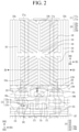
In this specification, the meaning of the pixel includes the area occupied by one transistor and the pixel electrode 2 connected thereto, and FIG. 2 shows one pixel.
FIG. 2 is a layout view of one pixel disposed in a first region A1. FIG. 3A is a cross-sectional view of a display device of FIG. 2 taken along a line IIIa-IIIa′. FIG. 3B is a cross-sectional view of a display device of FIG. 2 taken along a line IIIb-IIIb′.
Referring to FIG. 2 and FIG. 3A, a plurality of gate lines 121 disposed on a first substrate 110 made of transparent glass or plastic are included.
The gate lines 121 transmit a gate signal and extend in a first direction DR1. Each gate line 121 includes a first gate line 121 a and a second gate line 121 b that are separated from each other, and a gate electrode 124 connecting the first gate line 121 a and the second gate line 121 b.
Also, a storage electrode line 129 may be disposed on the same layer as the gate line 121. The storage electrode line 129 includes a first storage electrode line 129 a, a second storage electrode line 129 b, and a third storage electrode line 129 c extending in the second direction DR2, and the first storage electrode line 129 a, the second storage electrode line 129 b, and the third storage electrode line 129 c are connected to a transverse storage electrode line 129 d extending parallel to the first direction DR1. The second storage electrode line 129 b may include two parts that are separated from each other, and the second storage electrode line 129 b that is not connected to the transverse storage electrode line 129 d may be disposed with an island shape.
A gate insulating layer 140 made of an insulating material such as a silicon oxide or a silicon nitride is disposed on the gate line 121 and the storage electrode line 129. The gate insulating layer 140 may have a multilayered structure including at least two insulating layers having different physical properties.
A plurality of semiconductor layers 154 are disposed on the gate insulating layer 140. The semiconductor layer 154 may be disposed overlapping the gate electrode 124. Also, dummy semiconductor layers 155 disposed on the same layer as the semiconductor layer 154 may be disposed at a position where the gate line 121 and the data line 171 are crossed and a position where the storage electrode line 129 and the data line 171 are crossed. These dummy semiconductor layers 155 smooth a step at the region where the wires are crossed. However, the dummy semiconductor layer 155 does not constitute a transistor or the like.
Next, a plurality of data lines 171, a plurality of source electrodes 173 connected to the data lines 171, and a plurality of drain electrodes 175 are disposed on the semiconductor layer 154 and the gate insulating layer 140.
The data line 171 extends in the second direction DR2, thereby crossing the gate line 121. The data line 171 includes a first data line 171 a and a second data line 171 b. The first data line 171 a and the second data line 171 b overlap the pixel electrode 191, and are disposed without overlapping the storage electrode line 129.
In detail, the first data line 171 a may be disposed between the first storage electrode line 129 a and the second storage electrode line 129 b. Also, the second data line 171 b may be disposed between the second storage electrode line 129 b and the third storage electrode line 129 c.
The first data line 171 a each constitutes a respective transistor of the overlapping pixels. However, the second data line 171 b constitutes the transistors of other pixels (not shown) neighboring in the second direction. That is, in the present embodiment, two data lines overlap one pixel electrode 191, but only one data line 171 a is electrically connected to the pixel electrode 191 and the other data line 171 b is electrically connected to the pixel electrode neighboring thereto.
The second data line 171 b may be disposed to be curved and/or bent near the edge of the pixel electrode 191 in the second direction DR2. The first data line 171 a may be also disposed to be curved near the edge of the pixel electrode 191 in the second direction DR2. At this time, the curved length 312 b of the second data line 171 b may be longer than the curved length 312 a of the first data line 171 a (e.g., the length of the bent portion of the second data line 171 b may be longer than the bent portion of the first data line 171 a).
A portion of the first data line 171 a constitutes the source electrode 173. The source electrode 173 extends from the data line 171 and overlaps the gate electrode 124, and may have an approximate U-shape. The drain electrode 175 is separated from the data line 171, and extends from the center of the U-shape of the source electrode 173 toward the top.
One gate electrode 124, one source electrode 173, and one drain electrode 175 form one thin film transistor (TFT) together with the semiconductor layer 154, and the channel region of the thin film transistor is formed in the semiconductor layer 154 between the source electrode 173 and the drain electrodes 175.
Next, a plurality of color filters 230 are disposed on the data line 171. The color filters may include a red color filter, a green color filter, and a blue color filter. Each color filter may be located in the region corresponding to one pixel electrode 191.
Next, an insulating layer 180 is disposed. The insulating layer 180 may be made of an inorganic insulator such as a silicon nitride or a silicon oxide, an organic insulator, or a low dielectric constant insulator.
The insulating layer 180 and the color filter 230 include a contact hole 181 overlapping the drain electrode 175. The pixel electrode 191 is physically and electrically connected to the drain electrode 175 through the contact hole 181, thereby receiving the data voltage from the drain electrode 175.
The pixel electrode 191 may include a transparent conductor such as ITO or IZO. The pixel electrode includes a transverse stem part 192 extending in the first direction DR1, and a longitudinal stem part 193 crossing the transverse stem part and extending in the second direction DR2. Fine branches 199 extend from each stem part.
The pixel electrode 191 overlaps both the first storage electrode line 129 a and the third storage electrode line 129 c, and includes an outer longitudinal stem part 195 extending along the second direction DR2. The outer longitudinal stem part 195 is connected to the edge of the transverse stem part 192 of the pixel electrode 191.
The pixel electrode 191 also includes an outer transverse stem part 196. The outer transverse stem part 196 is disposed adjacent to the transistor TFT, and a part of the outer transverse stem part 196 is connected to the drain electrode 175 through the contact hole 181, thereby receiving the voltage.
A part of the outer transverse stem part 196 includes a first protrusion 196 a that overlaps the first data line 171 a and a second protrusion 196 b that overlaps the second data lines. The first data line 171 a and the first protrusion 196 a overlapping each other form a self-capacitance Cdp1. The second data line 171 b and the second protrusion 196 b overlapping each other constitute the neighboring-capacitance Cdp2.
Referring to FIG. 2, FIG. 1, the area of the second protrusion 196 b is larger than the area of the first protrusion 196 a. Therefore, the value of the neighboring-capacitance Cdp2 between the second protrusion 196 b and the second data line 171 b is larger than the value of the self-capacitance Cdp1. In the pixel disposed in the first region A1 of the display device, as shown in FIG. 1, the value of the neighboring-capacitance Cdp2 is larger than the value of the self-capacitance Cdp1 such that the luminance deviation due to the data voltage may be compensated. Specific effects will be described later.
Referring to FIG. 2, an overlapping pixel electrode 197 overlapping the part of the gate line 121 is included. The overlapping pixel electrode 197 may extend along the first direction DR1.
Next, referring to FIG. 2 and FIG. 3A, a light blocking member 220 is disposed on the pixel electrode 191. The light blocking member 220 is disposed along the first direction DR1, and overlaps the transistor and the gate line 121 and the like. In FIG. 2, the region overlapping the light blocking member 220 is referred to as a light blocking area, and the region not overlapping the light blocking member 220 is referred to as a display area.
Next, referring to FIG. 3A, a common electrode 270 is disposed on a second substrate 210. A liquid crystal layer 3 including liquid crystal molecules 31 is disposed between a first display panel 100 and a second display panel 200.
FIG. 3B shows another cross-section of FIG. 2. Referring to FIG. 3B, the first storage electrode line 129 a, the second storage electrode line 129 b, and the third storage electrode line 129 c are disposed to be separated from each other on the first substrate 110, and the first data line 171 a and the second data line 171 b are disposed therebetween. The description of the other constituent elements is the same as that in FIG. 3A such that the detailed explanations of the same constituent elements are omitted.
Next, the arrangement of one pixel disposed in the second region A2 of FIG. 1 is described with reference to FIG. 4. FIG. 4 is a layout view of one pixel disposed in the second region A2. Referring to FIG. 4, the arrangement of the pixel disposed in the second region A2 is the same as that in FIG. 2 except for the configuration related to the first protrusion 196 a of the outer transverse stem part 196. The detailed description of the same constituent elements is omitted.
Referring to FIG. 4, in the pixel according to the present embodiment, the outer transverse stem part 196 only includes the first protrusion 196 a without the second protrusion. Therefore, the first protrusion 196 a and the first data line 171 form the self-capacitance Cdp1, and the value of the self-capacitance Cdp1 becomes larger than the value of the neighboring-capacitance Cdp2. In the present embodiment, the second protrusion is not disposed. However, the outer transverse stem part 196 and the second data line 171 b are partially overlapped, thereby forming the neighboring-capacitance Cdp2 in the overlapping region. However, because the second data line 171 b does not include the configuration corresponding to the first protrusion 196 a overlapping the first data line 171 a, the self-capacitance Cdp1 is larger than the neighboring-capacitance Cdp2.
Also, the area 304 of the first protrusion 196 a intersecting with the first data line 171 a of FIG. 4 is larger than the area 302 of the first protrusion 196 a intersecting with the first data line 171 a of FIG. 2. The first protrusion 196 a of FIG. 2 is the structure disposed to compensate the capacitance by the curved part of the second data line 171 b because the second data line 171 b is curved near the edge of the pixel electrode 191 in the second direction DR2. Accordingly, in the pixel of FIG. 4, the area 304 of the first protrusion 196 a intersecting with the first data line 171 a should be larger than the area 302 that in the pixel of FIG. 2, and in this case, the self-capacitance Cdp1 becomes larger than the neighboring-capacitance Cdp2.
That is, in the display device according to the present embodiment, the pixel disposed in the first region A1 further includes the second protrusion overlapping the second data line such that the neighboring-capacitance Cdp2 is larger than the self-capacitance Cdp1, and in the pixel disposed in the second region A2, the area of the first protrusion overlapping the first data line is further wider without including the second protrusion, such that the self-capacitance Cdp1 is larger than the neighboring-capacitance Cdp2. Thus, since the sizes of the self-capacitance Cdp1 and the neighboring-capacitance Cdp2 are different from each other, the luminance deviation due to the data voltage may be compensated.
FIG. 5 shows various causes that affect a luminance and results in a display device. Referring to FIG. 5, when displaying an image in which a white box is disposed at the center, if the self-capacitance Cdp1 is large, the image appears bright at the top of the white box and dark at the bottom. Conversely, if the self-capacitance Cdp1 decreases, the image appears dark at the top of the white box and bright at the bottom.
The luminance of the display device is also affected by TFT leakage and the data voltage. Particularly, in the display device according to the present embodiment, since the data line 171 and the pixel electrode 191 are overlapped in the display area, the effect of the luminance due to the data voltage is great. Referring to FIG. 5, the change in the luminance due to the data voltage appears bright at the top and bottom of the white box.
Thus, the data voltage causes a problem that the display device is visibly brighter at the top and bottom of the white box. However, in the display device according to the present embodiment, the self-capacitance Cdp1 is made smaller than the neighboring-capacitance Cdp2 at the top of the white box, that is, at the top of the display device, so that the display device is recognized to be darkened, thereby compensating the luminance brightened by the data voltage. Also, the self-capacitance Cdp1 is made larger than the neighboring-capacitance Cdp2 at the bottom of the white box, that is, at the bottom of the display device, so that the display device is recognized to be darkened, thereby compensating the luminance brightened by the data voltage.
FIGS. 6A and 6B are views for measuring a luminance of a display device when displaying an image without a white box. FIG. 6A shows a measuring position, and FIG. 6B is an image for measuring a luminance at a measuring position. FIG. 6A shows a display panel 1000 and a pad 700. Referring to FIG. 6B, it is confirmed that there is no luminance deviation according to the position in the pixel in the image without the white box.
FIGS. 7A, 7B, 7C, and 7D are views for measuring a luminance of a display device when displaying an image including a white box. FIG. 7A shows a measuring position, and FIG. 7B is an image for measuring a luminance at a measuring position. FIG. 7A shows the display panel 1000 and the pad 700. Referring to FIG. 7B, in the case of the image including the white box, it may be confirmed that the luminance deviation appears for each position in the pixel. FIG. 7C shows a luminance for each position for the same cross-section as in FIG. 3B. Referring to FIG. 7C, it may be confirmed that the luminance is high near the first data line 171 a which is electrically connected to the pixel electrode 191, and the luminance is low near the second data line 171 b which is not electrically connected to the pixel electrode 191.
FIG. 7D shows a reason why a luminance is high near the first data line 171 a and a luminance is low near the second data line 171 b. Referring to FIG. 7D, potential increases near the first data line 171 a connected to the pixel electrode to supply a data voltage of 15 V such that the luminance is high. However, the potential decreases near the second data line 171 b to which the data voltage is not supplied during the driving of the corresponding pixel that is connected to the neighboring pixel electrode, and accordingly, the luminance is lower.
FIGS. 8A, 8B, and 8C are views showing a luminance in an upper and lower region of a white box of a display device when a self-capacitance Cdp1 is larger than a neighboring-capacitance Cdp2. FIG. 8A is a view showing a brightness in an upper end and a lower end of a white box when a self-capacitance Cdp1 is larger than a neighboring-capacitance Cdp2. FIG. 8A shows the display panel 1000 and the pad 700. Referring to FIG. 8A, the top of the white box appears lighter, and the bottom of the white box appears darker. FIG. 8B is a view showing a voltage behavior in an upper end of a white box. As shown in FIG. 8B, at the top of the white box, the image appears bright because the data voltages are driven in the direction away from each other. FIG. 8C shows the voltage behavior at the bottom of the white box. As shown in FIG. 8C, at the bottom of the white box, the data voltages are driven in the direction toward each other such that the image appears dark.
FIGS. 9A, 9B, and 9C are views showing a luminance in an upper and lower region of a white box of a display device when a self-capacitance Cdp1 is smaller than a neighboring-capacitance Cdp2. FIG. 9A is a view showing a brightness in an upper end and a lower end of a white box when a self-capacitance Cdp1 is smaller than a neighboring-capacitance Cdp2. FIG. 9A shows the display panel 1000 and the pad 700. Referring to FIG. 9A, the top of the white box appears darker, and the bottom of the white box appears lighter. FIG. 9B is a view showing a voltage behavior in an upper end of a white box. As shown in FIG. 9B, at the top of the white box, the image appears dark because the data voltages are driven in the direction approaching each other. FIG. 9C is a view showing a voltage behavior in a lower end of a white box. As shown in FIG. 9C, at the bottom of the white box, the image appears dark because the data voltages are driven in the direction away from each other.
That is, in the display device according to the present embodiment, by using a phenomenon that the luminance at the upper and lower ends of the white box varies depending on the magnitude difference of the self-capacitance Cdp1 and the neighboring-capacitance Cdp2, the luminance of the entire display device increases by the data voltage, thereby solving the phenomenon of being displayed brightly.
That is, in order to compensate the bright luminance, when the self-capacitance Cdp1 and the neighboring-capacitance Cdp2 are appropriately adjusted so as to lower the luminance, the luminance brightness due to the data voltage is compensated.
At this time, there is a difference in the method of reducing the luminance per region based on the center of the display device. That is, referring to FIG. 5, the self-capacitance Cdp1 should be smaller than the neighboring-capacitance Cdp2 to reduce the luminance of the top of the display device, that is, the top of the white box. Therefore, to increase the neighboring-capacitance Cdp2, as shown in FIG. 2, the second protrusion 196 b is added.
Again referring to FIG. 5, to reduce the luminance at the bottom of the display device, that is, the bottom of the white box, the self-capacitance Cdp1 should be smaller than the neighboring-capacitance Cdp2. Accordingly, to increase the self-capacitance Cdp1, as shown in FIG. 4, the area of the first protrusion 196 a is increased.
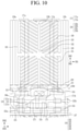
In the above, the embodiment adjusting the self-capacitance Cdp1 and the neighboring-capacitance Cdp2 by using the first protrusion 196 a and the second protrusion 196 b as the part of the pixel electrode 191 was described. However, the self-capacitance Cdp1 and the neighboring-capacitance Cdp2 may be adjusted by controlling the width of the data line, not the pixel electrode 191.
FIG. 10 and FIG. 11 are views showing a pixel disposed in a first region A1 and a second region A2 in a display device according to another embodiment.
FIG. 10 is a top plan view of the pixel disposed in the first region A1, and FIG. 11 is a top plan view of the pixel disposed in the second region A2.
Referring to FIG. 10, in the pixel according to the present embodiment, the width 322 b of the second data line 171 b expands in the region overlapping the light blocking member 220. In other words, by increasing the width 322 b of the second data line 171 b without adding the configuration of the separate protrusion in the same layer as the pixel electrode 191, the overlap area of the existing pixel electrode 191 and the second data line 171 b is increased. The width 322 a of the first data line 171 a is narrower than the width 322 b of the second data line 171 b. Therefore, since like FIG. 2 the neighboring-capacitance Cdp2 is larger than the self-capacitance Cdp1 and is in the upper region of the display device, the luminance is decreased in this case as confirmed from FIG. 5, and it is possible to compensate the luminance increase due to the data voltage. Other configurations are the same as those described above, and the detailed description of the same constituent elements is omitted.
Referring to FIG. 11, in the pixel according to the present embodiment, the width of the first data line 171 a extends in the region overlapping the light blocking member 220. That is, without changing the area of the first protrusion 196 a, by increasing the width of the first data line 171 a, the overlapping area of the pixel electrode 191 and the first data line 171 a increases. Accordingly, the self-capacitance Cdp1 is larger than the neighboring-capacitance Cdp2. Since the second region A2 is the lower end region of the display device, the luminance decreases as confirmed in FIG. 5, and accordingly, like in FIG. 4, the luminance increase of the data voltage may be compensated. Other configurations are the same as those described above, and the detailed description of the same constituent elements is omitted.
In the above, in the configuration in which the display device is divided into the first region A1 and the second region A2, the self-capacitance Cdp1 is smaller than the neighboring-capacitance Cdp2 in the first region A1, and the self-capacitance Cdp1 is larger than the neighboring-capacitance Cdp2 in the second region A2. However, in another embodiment, the difference between the self-capacitance Cdp1 and the neighboring-capacitance Cdp2 may increase and decrease stepwise.
FIG. 12 is a view showing a display device 1000 according to another embodiment of the present inventive concept. Referring to FIG. 12, the difference between the self-capacitance Cdp1 and neighboring-capacitance Cdp2 is greatest in the uppermost region divided by the center of the display device 1000. However, the difference between the self-capacitance Cdp1 and the neighboring-capacitance Cdp2 decreases toward the center, and the self-capacitance Cdp1 and the neighboring-capacitance Cdp2 become equal at the center of the display device.
While passing through the center of the display device 1000, the self-capacitance Cdp1 is larger than the neighboring-capacitance Cdp2 at the lower side, and the difference therebetween increases farther away from the center. If the difference between the self-capacitance Cdp1 and the neighboring-capacitance Cdp2 is adjusted stepwise, the increase in luminance due to the data voltage may be effectively compensated.
The values of the self-capacitance Cdp1 and the neighboring-capacitance Cdp2 may be adjusted in various ways. That is, as shown in FIG. 2 to FIG. 4, these values may be adjusted by using the areas of the first protrusion 196 a and the second protrusion 196 b that are disposed on the same layer as the pixel electrode 191, and as shown in FIG. 10 and FIG. 11, by using the widths of the first data line 171 a and the second data line 171 b.
Since the capacitance increases as the area of the protrusion is larger or the width of the data line increases, a person of ordinary skill in the art may adjust the capacitance by increasing or decreasing the area or width stepwise by each region of the display device 1000.
While this invention has been described in connection with what is presently considered to be practical embodiments, it is to be understood that the invention is not limited to the disclosed embodiments. On the contrary, it is intended to cover various modifications and equivalent arrangements included within the spirit and scope of the appended claims.

Claims (10)

What is claimed is:
1. A display device comprising:
a substrate including a first region and a second region; and
a plurality of pixels disposed on the substrate,
wherein the plurality of pixels each include a first data line and a second data line overlapping a pixel electrode,
a first capacitance between the first data line and the pixel electrode is smaller than a second capacitance between the second data line and the pixel electrode in a pixel disposed in the first region, and
the first capacitance between the first data line and the pixel electrode is larger than the second capacitance between the second data line and the pixel electrode in a pixel disposed in the second region,
wherein a pixel electrode protrusion is connected to the pixel electrode,
an area of a first pixel electrode protrusion overlapping the first data line in the pixel disposed in the second region is wider than an area of a first pixel electrode protrusion overlapping the first data line of the pixel disposed in the first region,
the first data line and the second data line are curved at one edge of the pixel electrode, and
a curved length of the second data line is longer than a curved length of the first data line.
2. The display device of claim 1, wherein
the display panel is scanned in a direction from the first region to the second region.
3. The display device of claim 1, wherein
the plurality of pixels each include:
a gate line disposed on the substrate; and
a data line disposed to be insulated from the gate line,
wherein the data line includes the first data line and the second data line, and
the pixel disposed in the first region includes a second pixel electrode protrusion overlapping the second data line.
4. The display device of claim 3, further comprising
a storage electrode line disposed on the same layer as the gate line,
wherein the storage electrode line includes a first storage electrode line, a second storage electrode line, and a third storage electrode line,
the first storage electrode line is disposed to be adjacent to one edge of the pixel electrode,
the third storage electrode line is disposed to be adjacent to another edge of the pixel electrode, and
the second storage electrode line is disposed to overlap the center of the pixel electrode.
5. The display device of claim 4, wherein
the first data line is disposed between the first storage electrode line and the second storage electrode line, and
the second data line is disposed between the second storage electrode line and the third storage electrode line.
6. The display device of claim 1, wherein
the first data line is electrically connected to the pixel electrode of the pixel, and
the second data line is not electrically connected to the pixel electrode that is electrically connected to the first data line.
7. The display device of claim 6, wherein
the pixel includes a display area and a light blocking area, and
in the light blocking area of the pixel disposed in the first region, a width of the first data line is narrower than a width of the second data line.
8. The display device of claim 7, wherein
in the light blocking area of the pixel disposed in the second region, the width of the first data line is wider than the width of the second data line.
9. The display device of claim 1, further comprising
a plurality of semiconductor layers disposed between the gate line and the data line,
wherein the plurality of semiconductor layers each include a dummy semiconductor layer disposed at a region where the gate line and the data line cross each other.
10. The display device of claim 9, wherein
the gate line includes a first gate line and a second gate line parallel to each other, and a gate electrode disposed between the first gate line and the second gate line, and
a part of the plurality of semiconductor layers is disposed to overlap the gate electrode so as to configure a transistor.
US16/802,442 2019-04-30 2020-02-26 Display device Active US11226527B2 (en)

Priority Applications (1)

Application Number Priority Date Filing Date Title
US17/543,725 US11762251B2 (en) 2019-04-30 2021-12-06 Display device

Applications Claiming Priority (2)

Application Number Priority Date Filing Date Title
KR10-2019-0050337 2019-04-30
KR1020190050337A KR20200127073A (en) 2019-04-30 2019-04-30 Display device

Related Child Applications (1)

Application Number Title Priority Date Filing Date
US17/543,725 Division US11762251B2 (en) 2019-04-30 2021-12-06 Display device

Publications (2)

Publication Number Publication Date
US20200348571A1 US20200348571A1 (en) 2020-11-05
US11226527B2 true US11226527B2 (en) 2022-01-18

Family

ID=72984954

Family Applications (2)

Application Number Title Priority Date Filing Date
US16/802,442 Active US11226527B2 (en) 2019-04-30 2020-02-26 Display device
US17/543,725 Active US11762251B2 (en) 2019-04-30 2021-12-06 Display device

Family Applications After (1)

Application Number Title Priority Date Filing Date
US17/543,725 Active US11762251B2 (en) 2019-04-30 2021-12-06 Display device

Country Status (3)

Country Link
US (2) US11226527B2 (en)
KR (1) KR20200127073A (en)
CN (1) CN111856827A (en)

Families Citing this family (1)

* Cited by examiner, † Cited by third party
Publication number Priority date Publication date Assignee Title
KR20210127842A (en) * 2020-04-14 2021-10-25 삼성디스플레이 주식회사 Liquid crystal device

Citations (12)

* Cited by examiner, † Cited by third party
Publication number Priority date Publication date Assignee Title
US6429907B1 (en) * 1999-02-24 2002-08-06 Lg Philips Lcd Co., Ltd. Liquid crystal display having improved image quality by reducing the excited interference voltage
KR100905015B1 (en) 2002-12-26 2009-06-30 엘지디스플레이 주식회사 Liquid crystal display device for preventing overbrightness of most outer pixels
US20100073273A1 (en) * 2008-09-23 2010-03-25 Chul Nam Liquid crystal panel and liquid crystal display device having the same
KR101240646B1 (en) 2005-09-07 2013-03-08 삼성디스플레이 주식회사 Liquid crystal display
US20130215344A1 (en) * 2009-05-19 2013-08-22 Samsung Display Co., Ltd. Liquid crystal display
US20160147119A1 (en) * 2014-11-21 2016-05-26 Samsung Display Co., Ltd. Liquid crystal display
KR101641538B1 (en) 2008-12-24 2016-07-22 삼성디스플레이 주식회사 Display panel
US20160313613A1 (en) * 2015-04-22 2016-10-27 Au Optronics Corp. Pixel structure and display panel
KR20170039000A (en) 2015-09-30 2017-04-10 엘지디스플레이 주식회사 Array Substrate For Liquid Crystal Display Device
US10281784B1 (en) * 2017-12-06 2019-05-07 Samsung Display Co., Ltd. Liquid crystal display device
US20190296048A1 (en) * 2018-03-22 2019-09-26 Samsung Display Co., Ltd, Display device
US20190355318A1 (en) * 2018-05-17 2019-11-21 Samsung Display Co., Ltd. Display device

Family Cites Families (7)

* Cited by examiner, † Cited by third party
Publication number Priority date Publication date Assignee Title
JP2004133028A (en) * 2002-10-08 2004-04-30 Toshiba Matsushita Display Technology Co Ltd Liquid crystal display device
KR100898785B1 (en) * 2002-10-24 2009-05-20 엘지디스플레이 주식회사 Liquid crystal display
JP3958306B2 (en) * 2003-09-02 2007-08-15 シャープ株式会社 Liquid crystal display
JP4276965B2 (en) * 2004-02-04 2009-06-10 シャープ株式会社 Display device
US8334954B2 (en) * 2006-04-04 2012-12-18 Sharp Kabushiki Kaisha Liquid crystal display device
WO2012093621A1 (en) * 2011-01-06 2012-07-12 シャープ株式会社 Liquid-crystal display device
US9495923B2 (en) * 2011-05-18 2016-11-15 Sharp Kabushiki Kaisha Liquid crystal display device, method of driving liquid crystal display device, and television receiver

Patent Citations (12)

* Cited by examiner, † Cited by third party
Publication number Priority date Publication date Assignee Title
US6429907B1 (en) * 1999-02-24 2002-08-06 Lg Philips Lcd Co., Ltd. Liquid crystal display having improved image quality by reducing the excited interference voltage
KR100905015B1 (en) 2002-12-26 2009-06-30 엘지디스플레이 주식회사 Liquid crystal display device for preventing overbrightness of most outer pixels
KR101240646B1 (en) 2005-09-07 2013-03-08 삼성디스플레이 주식회사 Liquid crystal display
US20100073273A1 (en) * 2008-09-23 2010-03-25 Chul Nam Liquid crystal panel and liquid crystal display device having the same
KR101641538B1 (en) 2008-12-24 2016-07-22 삼성디스플레이 주식회사 Display panel
US20130215344A1 (en) * 2009-05-19 2013-08-22 Samsung Display Co., Ltd. Liquid crystal display
US20160147119A1 (en) * 2014-11-21 2016-05-26 Samsung Display Co., Ltd. Liquid crystal display
US20160313613A1 (en) * 2015-04-22 2016-10-27 Au Optronics Corp. Pixel structure and display panel
KR20170039000A (en) 2015-09-30 2017-04-10 엘지디스플레이 주식회사 Array Substrate For Liquid Crystal Display Device
US10281784B1 (en) * 2017-12-06 2019-05-07 Samsung Display Co., Ltd. Liquid crystal display device
US20190296048A1 (en) * 2018-03-22 2019-09-26 Samsung Display Co., Ltd, Display device
US20190355318A1 (en) * 2018-05-17 2019-11-21 Samsung Display Co., Ltd. Display device

Also Published As

Publication number Publication date
US20200348571A1 (en) 2020-11-05
US20220107537A1 (en) 2022-04-07
CN111856827A (en) 2020-10-30
KR20200127073A (en) 2020-11-10
US11762251B2 (en) 2023-09-19

Similar Documents

Publication Publication Date Title
US9213205B2 (en) Liquid crystal display having multiple pixel regions for improved transmittance
US10651207B2 (en) Display device having a scanning circuit disposed along an edge of a substrate and scan lines connected to the scanning circuit
JP4707980B2 (en) Thin film transistor display panel
US8988621B2 (en) Array substrate and display panel having the same
US8477252B2 (en) Display apparatus with gate leading lines of differing lengths
KR102652674B1 (en) Ultra High Resolution Liquid Crystal Display
US10622384B2 (en) Liquid crystal display panel and liquid crystal display
US9766525B2 (en) Active-matrix substrate and display device
KR102031682B1 (en) Ultra High Resolution Liquid Crystal Display Having A Compensating Thin Film Transistor At Each Pixel
US10564489B2 (en) Liquid crystal display device
US10809579B2 (en) Liquid crystal display
US11762251B2 (en) Display device
JP5868993B2 (en) Liquid crystal display element and liquid crystal display device
JP5815127B2 (en) Liquid crystal display element and liquid crystal display device
CN107544186A (en) Display device
US20160202585A1 (en) Liquid crystal display
US11537012B2 (en) Substrate for display device and display device
KR102162754B1 (en) Ultra High Resolution Liquid Crystal Display Having A Compensating Thin Film Transistor
KR102346086B1 (en) Liquid crystal display device having a compensting thin film transistor
KR20080098882A (en) Liquid crystal display
KR102202453B1 (en) Ultra High Resolution Liquid Crystal Display Having A Compensating Thin Film Transistor
US9397120B2 (en) Array substrate and a display device having the same
JP2023114224A (en) Semiconductor device and display

Legal Events

Date Code Title Description
AS Assignment

Owner name: SAMSUNG DISPLAY CO., LTD., KOREA, REPUBLIC OF

Free format text: ASSIGNMENT OF ASSIGNORS INTEREST;ASSIGNORS:RYU, GWON-HEON;KIM, KWI HYUN;CHOI, KOOK HYUN;AND OTHERS;REEL/FRAME:051942/0775

Effective date: 20191028

FEPP Fee payment procedure

Free format text: ENTITY STATUS SET TO UNDISCOUNTED (ORIGINAL EVENT CODE: BIG.); ENTITY STATUS OF PATENT OWNER: LARGE ENTITY

STPP Information on status: patent application and granting procedure in general

Free format text: NON FINAL ACTION MAILED

STPP Information on status: patent application and granting procedure in general

Free format text: RESPONSE TO NON-FINAL OFFICE ACTION ENTERED AND FORWARDED TO EXAMINER

STPP Information on status: patent application and granting procedure in general

Free format text: FINAL REJECTION MAILED

STPP Information on status: patent application and granting procedure in general

Free format text: ADVISORY ACTION MAILED

STPP Information on status: patent application and granting procedure in general

Free format text: DOCKETED NEW CASE - READY FOR EXAMINATION

STPP Information on status: patent application and granting procedure in general

Free format text: NOTICE OF ALLOWANCE MAILED -- APPLICATION RECEIVED IN OFFICE OF PUBLICATIONS

STPP Information on status: patent application and granting procedure in general

Free format text: PUBLICATIONS -- ISSUE FEE PAYMENT VERIFIED

STCF Information on status: patent grant

Free format text: PATENTED CASE