US11091850B2 - Producing method of wired circuit board - Google Patents
Producing method of wired circuit board Download PDFInfo
- Publication number
- US11091850B2 US11091850B2 US15/876,603 US201815876603A US11091850B2 US 11091850 B2 US11091850 B2 US 11091850B2 US 201815876603 A US201815876603 A US 201815876603A US 11091850 B2 US11091850 B2 US 11091850B2
- Authority
- US
- United States
- Prior art keywords
- gold plating
- stainless steel
- layer
- gold
- plating layer
- Prior art date
- Legal status (The legal status is an assumption and is not a legal conclusion. Google has not performed a legal analysis and makes no representation as to the accuracy of the status listed.)
- Active, expires
Links
Images


Classifications
-
- C—CHEMISTRY; METALLURGY
- C25—ELECTROLYTIC OR ELECTROPHORETIC PROCESSES; APPARATUS THEREFOR
- C25D—PROCESSES FOR THE ELECTROLYTIC OR ELECTROPHORETIC PRODUCTION OF COATINGS; ELECTROFORMING; APPARATUS THEREFOR
- C25D5/00—Electroplating characterised by the process; Pretreatment or after-treatment of workpieces
- C25D5/02—Electroplating of selected surface areas
-
- C—CHEMISTRY; METALLURGY
- C25—ELECTROLYTIC OR ELECTROPHORETIC PROCESSES; APPARATUS THEREFOR
- C25D—PROCESSES FOR THE ELECTROLYTIC OR ELECTROPHORETIC PRODUCTION OF COATINGS; ELECTROFORMING; APPARATUS THEREFOR
- C25D5/00—Electroplating characterised by the process; Pretreatment or after-treatment of workpieces
- C25D5/10—Electroplating with more than one layer of the same or of different metals
-
- C—CHEMISTRY; METALLURGY
- C25—ELECTROLYTIC OR ELECTROPHORETIC PROCESSES; APPARATUS THEREFOR
- C25D—PROCESSES FOR THE ELECTROLYTIC OR ELECTROPHORETIC PRODUCTION OF COATINGS; ELECTROFORMING; APPARATUS THEREFOR
- C25D3/00—Electroplating: Baths therefor
- C25D3/02—Electroplating: Baths therefor from solutions
- C25D3/48—Electroplating: Baths therefor from solutions of gold
-
- C—CHEMISTRY; METALLURGY
- C25—ELECTROLYTIC OR ELECTROPHORETIC PROCESSES; APPARATUS THEREFOR
- C25D—PROCESSES FOR THE ELECTROLYTIC OR ELECTROPHORETIC PRODUCTION OF COATINGS; ELECTROFORMING; APPARATUS THEREFOR
- C25D5/00—Electroplating characterised by the process; Pretreatment or after-treatment of workpieces
- C25D5/02—Electroplating of selected surface areas
- C25D5/022—Electroplating of selected surface areas using masking means
-
- C—CHEMISTRY; METALLURGY
- C25—ELECTROLYTIC OR ELECTROPHORETIC PROCESSES; APPARATUS THEREFOR
- C25D—PROCESSES FOR THE ELECTROLYTIC OR ELECTROPHORETIC PRODUCTION OF COATINGS; ELECTROFORMING; APPARATUS THEREFOR
- C25D5/00—Electroplating characterised by the process; Pretreatment or after-treatment of workpieces
- C25D5/34—Pretreatment of metallic surfaces to be electroplated
- C25D5/36—Pretreatment of metallic surfaces to be electroplated of iron or steel
-
- C—CHEMISTRY; METALLURGY
- C25—ELECTROLYTIC OR ELECTROPHORETIC PROCESSES; APPARATUS THEREFOR
- C25D—PROCESSES FOR THE ELECTROLYTIC OR ELECTROPHORETIC PRODUCTION OF COATINGS; ELECTROFORMING; APPARATUS THEREFOR
- C25D5/00—Electroplating characterised by the process; Pretreatment or after-treatment of workpieces
- C25D5/48—After-treatment of electroplated surfaces
- C25D5/50—After-treatment of electroplated surfaces by heat-treatment
-
- C—CHEMISTRY; METALLURGY
- C25—ELECTROLYTIC OR ELECTROPHORETIC PROCESSES; APPARATUS THEREFOR
- C25D—PROCESSES FOR THE ELECTROLYTIC OR ELECTROPHORETIC PRODUCTION OF COATINGS; ELECTROFORMING; APPARATUS THEREFOR
- C25D7/00—Electroplating characterised by the article coated
-
- H—ELECTRICITY
- H05—ELECTRIC TECHNIQUES NOT OTHERWISE PROVIDED FOR
- H05K—PRINTED CIRCUITS; CASINGS OR CONSTRUCTIONAL DETAILS OF ELECTRIC APPARATUS; MANUFACTURE OF ASSEMBLAGES OF ELECTRICAL COMPONENTS
- H05K1/00—Printed circuits
- H05K1/02—Details
- H05K1/03—Use of materials for the substrate
- H05K1/05—Insulated conductive substrates, e.g. insulated metal substrate
-
- H—ELECTRICITY
- H05—ELECTRIC TECHNIQUES NOT OTHERWISE PROVIDED FOR
- H05K—PRINTED CIRCUITS; CASINGS OR CONSTRUCTIONAL DETAILS OF ELECTRIC APPARATUS; MANUFACTURE OF ASSEMBLAGES OF ELECTRICAL COMPONENTS
- H05K3/00—Apparatus or processes for manufacturing printed circuits
- H05K3/10—Apparatus or processes for manufacturing printed circuits in which conductive material is applied to the insulating support in such a manner as to form the desired conductive pattern
- H05K3/18—Apparatus or processes for manufacturing printed circuits in which conductive material is applied to the insulating support in such a manner as to form the desired conductive pattern using precipitation techniques to apply the conductive material
- H05K3/188—Apparatus or processes for manufacturing printed circuits in which conductive material is applied to the insulating support in such a manner as to form the desired conductive pattern using precipitation techniques to apply the conductive material by direct electroplating
-
- H—ELECTRICITY
- H05—ELECTRIC TECHNIQUES NOT OTHERWISE PROVIDED FOR
- H05K—PRINTED CIRCUITS; CASINGS OR CONSTRUCTIONAL DETAILS OF ELECTRIC APPARATUS; MANUFACTURE OF ASSEMBLAGES OF ELECTRICAL COMPONENTS
- H05K3/00—Apparatus or processes for manufacturing printed circuits
- H05K3/22—Secondary treatment of printed circuits
- H05K3/24—Reinforcing of the conductive pattern
- H05K3/241—Reinforcing of the conductive pattern characterised by the electroplating method; means therefor, e.g. baths or apparatus
-
- H—ELECTRICITY
- H05—ELECTRIC TECHNIQUES NOT OTHERWISE PROVIDED FOR
- H05K—PRINTED CIRCUITS; CASINGS OR CONSTRUCTIONAL DETAILS OF ELECTRIC APPARATUS; MANUFACTURE OF ASSEMBLAGES OF ELECTRICAL COMPONENTS
- H05K3/00—Apparatus or processes for manufacturing printed circuits
- H05K3/22—Secondary treatment of printed circuits
- H05K3/24—Reinforcing of the conductive pattern
- H05K3/243—Reinforcing of the conductive pattern characterised by selective plating, e.g. for finish plating of pads
-
- H—ELECTRICITY
- H05—ELECTRIC TECHNIQUES NOT OTHERWISE PROVIDED FOR
- H05K—PRINTED CIRCUITS; CASINGS OR CONSTRUCTIONAL DETAILS OF ELECTRIC APPARATUS; MANUFACTURE OF ASSEMBLAGES OF ELECTRICAL COMPONENTS
- H05K3/00—Apparatus or processes for manufacturing printed circuits
- H05K3/46—Manufacturing multilayer circuits
- H05K3/4644—Manufacturing multilayer circuits by building the multilayer layer by layer, i.e. build-up multilayer circuits
-
- G—PHYSICS
- G11—INFORMATION STORAGE
- G11B—INFORMATION STORAGE BASED ON RELATIVE MOVEMENT BETWEEN RECORD CARRIER AND TRANSDUCER
- G11B5/00—Recording by magnetisation or demagnetisation of a record carrier; Reproducing by magnetic means; Record carriers therefor
- G11B5/48—Disposition or mounting of heads or head supports relative to record carriers ; arrangements of heads, e.g. for scanning the record carrier to increase the relative speed
- G11B5/4806—Disposition or mounting of heads or head supports relative to record carriers ; arrangements of heads, e.g. for scanning the record carrier to increase the relative speed specially adapted for disk drive assemblies, e.g. assembly prior to operation, hard or flexible disk drives
- G11B5/4833—Structure of the arm assembly, e.g. load beams, flexures, parts of the arm adapted for controlling vertical force on the head
-
- H—ELECTRICITY
- H05—ELECTRIC TECHNIQUES NOT OTHERWISE PROVIDED FOR
- H05K—PRINTED CIRCUITS; CASINGS OR CONSTRUCTIONAL DETAILS OF ELECTRIC APPARATUS; MANUFACTURE OF ASSEMBLAGES OF ELECTRICAL COMPONENTS
- H05K1/00—Printed circuits
- H05K1/02—Details
- H05K1/0277—Bendability or stretchability details
- H05K1/028—Bending or folding regions of flexible printed circuits
- H05K1/0281—Reinforcement details thereof
-
- H—ELECTRICITY
- H05—ELECTRIC TECHNIQUES NOT OTHERWISE PROVIDED FOR
- H05K—PRINTED CIRCUITS; CASINGS OR CONSTRUCTIONAL DETAILS OF ELECTRIC APPARATUS; MANUFACTURE OF ASSEMBLAGES OF ELECTRICAL COMPONENTS
- H05K1/00—Printed circuits
- H05K1/02—Details
- H05K1/03—Use of materials for the substrate
- H05K1/0393—Flexible materials
-
- H—ELECTRICITY
- H05—ELECTRIC TECHNIQUES NOT OTHERWISE PROVIDED FOR
- H05K—PRINTED CIRCUITS; CASINGS OR CONSTRUCTIONAL DETAILS OF ELECTRIC APPARATUS; MANUFACTURE OF ASSEMBLAGES OF ELECTRICAL COMPONENTS
- H05K1/00—Printed circuits
- H05K1/02—Details
- H05K1/03—Use of materials for the substrate
- H05K1/05—Insulated conductive substrates, e.g. insulated metal substrate
- H05K1/053—Insulated conductive substrates, e.g. insulated metal substrate the metal substrate being covered by an inorganic insulating layer
-
- H—ELECTRICITY
- H05—ELECTRIC TECHNIQUES NOT OTHERWISE PROVIDED FOR
- H05K—PRINTED CIRCUITS; CASINGS OR CONSTRUCTIONAL DETAILS OF ELECTRIC APPARATUS; MANUFACTURE OF ASSEMBLAGES OF ELECTRICAL COMPONENTS
- H05K1/00—Printed circuits
- H05K1/02—Details
- H05K1/03—Use of materials for the substrate
- H05K1/05—Insulated conductive substrates, e.g. insulated metal substrate
- H05K1/056—Insulated conductive substrates, e.g. insulated metal substrate the metal substrate being covered by an organic insulating layer
-
- H—ELECTRICITY
- H05—ELECTRIC TECHNIQUES NOT OTHERWISE PROVIDED FOR
- H05K—PRINTED CIRCUITS; CASINGS OR CONSTRUCTIONAL DETAILS OF ELECTRIC APPARATUS; MANUFACTURE OF ASSEMBLAGES OF ELECTRICAL COMPONENTS
- H05K1/00—Printed circuits
- H05K1/02—Details
- H05K1/11—Printed elements for providing electric connections to or between printed circuits
-
- H—ELECTRICITY
- H05—ELECTRIC TECHNIQUES NOT OTHERWISE PROVIDED FOR
- H05K—PRINTED CIRCUITS; CASINGS OR CONSTRUCTIONAL DETAILS OF ELECTRIC APPARATUS; MANUFACTURE OF ASSEMBLAGES OF ELECTRICAL COMPONENTS
- H05K2203/00—Indexing scheme relating to apparatus or processes for manufacturing printed circuits covered by H05K3/00
- H05K2203/11—Treatments characterised by their effect, e.g. heating, cooling, roughening
- H05K2203/1105—Heating or thermal processing not related to soldering, firing, curing or laminating, e.g. for shaping the substrate or during finish plating
-
- H—ELECTRICITY
- H05—ELECTRIC TECHNIQUES NOT OTHERWISE PROVIDED FOR
- H05K—PRINTED CIRCUITS; CASINGS OR CONSTRUCTIONAL DETAILS OF ELECTRIC APPARATUS; MANUFACTURE OF ASSEMBLAGES OF ELECTRICAL COMPONENTS
- H05K2203/00—Indexing scheme relating to apparatus or processes for manufacturing printed circuits covered by H05K3/00
- H05K2203/14—Related to the order of processing steps
- H05K2203/1476—Same or similar kind of process performed in phases, e.g. coarse patterning followed by fine patterning
Definitions
- the present invention relates to a method for producing a wired circuit board.
- a method in which a terminal for electrical connection is formed on a stainless steel board, and a gold plating layer is formed on the terminal by gold plating has been known.
- a forming method of a gold plating pattern on the stainless steel board has been proposed in which a desired site of the stainless steel board is immersed in a hydrochloric acid-based plating solution, and a first gold plating layer is formed on the immersed site (ref: for example, Japanese Unexamined Patent Publication No. 2014-34702).
- a conductive layer is separately provided on the stainless steel board, and a conductive terminal is provided on the conductive layer.
- a passive film is provided on the surface of the stainless steel board, so that in view of improvement of the adhesive properties described above, the removal of the passive film is required.
- the above-described passive film is removed by immersing the stainless steel board in the hydrochloric acid-based plating solution, and the gold plating layer is formed on the terminal of the stainless steel board.
- the gold plating layer is formed on the conductive terminal, and forming of the gold plating layer on the terminal of the stainless steel board and forming of the gold plating layer on the conductive terminal are performed by using the same plating bath.
- the conductive terminal is corroded by the hydrochloric acid-based plating solution.
- An object of the present invention is to provide a method for producing a wired circuit board capable of easily forming the first gold plating layer on the stainless steel terminal with easy equipment.
- the present invention [1] includes a method for producing a wired circuit board including a stainless steel supporting layer having a stainless steel terminal including a first step of preparing the stainless steel supporting layer having a passive film formed on the surface thereof and a second step of forming a first gold plating layer on the surface of the stainless steel terminal, wherein in the second step, the stainless steel supporting layer is immersed in a first gold plating solution containing a weak acid and a gold compound without containing a strong acid, and electricity is supplied to the stainless steel supporting layer so that the passive film is removed and the first gold plating layer is formed on the surface of the stainless steel terminal.
- the stainless steel supporting layer is immersed in the first gold plating solution containing the weak acid and the gold compound without containing the strong acid, so that in the second step, when the electricity is supplied to the stainless steel supporting layer, the passive film is surely removed and the first gold plating layer can be formed on the surface of the stainless steel terminal.
- the first gold plating solution does not contain the strong acid, so that when the first gold plating solution is used, the gold plating layer can be formed on the conductive terminal, while corrosion of the conductive terminal is suppressed. Thus, the first gold plating layer can be easily formed on the stainless steel terminal with easy equipment.
- the present invention [2] includes the method for producing a wired circuit board described in [1] further including: after the second step, a third step of forming a second gold plating layer on the surface of the first gold plating layer, wherein in the third step, the stainless steel supporting layer is immersed in a second gold plating solution containing a gold compound without containing an acid, and electricity is supplied to the stainless steel supporting layer so that the second gold plating layer is formed on the surface of the first gold plating layer; and the content ratio of the gold compound in the second gold plating solution is higher than that of the gold compound in the first gold plating solution.
- the content ratio of the gold compound in the second gold plating solution in the third step is higher than that of the gold compound in the first gold plating solution in the second step, so that the thick second plating layer can be efficiently formed for a short period of time.
- the present invention [3] includes the method for producing a wired circuit board described in [1] or [2], wherein the wired circuit board further includes a conductive layer supported by the stainless steel supporting layer and having a conductive terminal, further including: a fourth step of forming a third gold plating layer on the surface of the conductive terminal; wherein in the fourth step, the conductive layer is immersed in a third gold plating solution containing a weak acid and a gold compound without containing a strong acid, and electricity is supplied to the conductive layer so that the third gold plating layer is formed on the surface of the conductive terminal; and the ratio of the current density in the second step to the current density in the fourth step is 2 or more.
- the ratio of the current density in the second step to the current density in the fourth step is 2 or more. That is, the current density in the second step can be set higher than that in the fourth step, so that in the second step, the passive film can be further more surely removed. As a result, the wired circuit board including the first gold plating layer having adhesive properties with respect to the stainless steel terminal can be produced.
- the present invention [4] includes the method for producing a wired circuit board described in any one of [1] to [3], wherein the wired circuit board further includes a conductive layer supported by the stainless steel supporting layer and having a conductive terminal, further including: after the second step, a fourth step of forming a third gold plating layer on the surface of the conductive terminal; wherein in the fourth step, the conductive layer is immersed in a third gold plating solution containing a weak acid and a gold compound without containing a strong acid, and electricity is supplied to the conductive layer so that the third gold plating layer is formed on the surface of the conductive terminal; and the second step and the fourth step are performed in the same plating bath.
- the second step and the fourth step are performed in the same plating bath, so that a producing device and a producing step can be simplified.
- the present invention [5] includes the method for producing a wired circuit board described in any one of [1] to [4] further including: after the second step, a heating step of heating the first gold plating layer.
- the heating step the first gold plating layer is heated, so that the wired circuit board including the first gold plating layer having adhesive properties with respect to the stainless steel terminal can be produced.
- the present invention [6] includes the method for producing a wired circuit board described in [2] further including: after the third step, a heating step of heating the first gold plating layer and the second gold plating layer.
- the heating step in the heating step, the first gold plating layer and the second gold plating layer are heated, so that the wired circuit board including the first gold plating layer and the second gold plating layer that have adhesive properties with respect to the stainless steel terminal can be produced.
- the wired circuit board including the first gold plating layer having excellent adhesive properties with respect to the stainless steel terminal can be produced.
- FIGS. 1A to 1C show partial process drawings for illustrating a method for producing a suspension board with circuit that is one embodiment of a method for producing a wired circuit board of the present invention:
- FIG. 1A illustrating a first step of preparing a suspension board with circuit
- FIG. 1B illustrating a second step of forming a first gold plating layer
- FIG. 1C illustrating a third step of forming a second gold plating layer.
- FIGS. 2D to 2F subsequent to FIG. 1C , show partial process drawings for illustrating the method for producing a suspension board with circuit that is one embodiment of the method for producing a wired circuit board of the present invention:
- FIG. 2D illustrating a fourth step of preparing a third gold plating layer
- FIG. 2E illustrating a fifth step of forming a fourth gold plating layer
- FIG. 2F illustrating a sixth step of removing a second plating resist.
- FIG. 3 shows a flow chart of the method for producing a suspension board with circuit shown in FIGS. 1A to 2F .
- FIG. 4 shows a schematic drawing of a plating device used in the method for producing a suspension board with circuit.
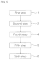
- FIG. 5 shows a flow chart of a modified example (embodiment in which the third step is not performed) of the method for producing a suspension board with circuit.
- FIG. 6 shows a flow chart of a modified example (embodiment in which the second step and the sixth step are sequentially performed) of the method for producing a suspension board with circuit.
- FIG. 7 shows a flow chart of a modified example (embodiment in which the third step and the sixth step are sequentially performed) of the method for producing a suspension board with circuit.
- FIGS. 8A and 8B show partial process drawings of a modified example (method for producing a first suspension board with circuit without including a third gold plating layer and a fourth gold plating layer on a conductive terminal) of the method for producing a suspension board with circuit:
- FIG. 8A illustrating a second step of forming a first gold plating layer
- FIG. 8B illustrating a third step of forming a second gold plating layer.
- FIGS. 9A and 9B show partial process drawings of a modified example (method for producing a second suspension board with circuit without including a first gold plating layer and a second gold plating layer on a stainless steel terminal) of the method for producing a suspension board with circuit:
- FIG. 9A illustrating a fourth step of preparing a third gold plating layer
- FIG. 9B illustrating a fifth step of forming a fourth gold plating layer.
- a method for producing a suspension board with circuit that is one embodiment of a method for producing a wired circuit board of the present invention is a method for producing a suspension board with circuit 21 including a stainless steel supporting layer 22 and a conductive layer 24 .
- the suspension board with circuit 21 sequentially includes the stainless steel supporting layer 22 , a base insulating layer 23 , the conductive layer 24 , and a cover insulating layer (not shown) in a thickness direction (up-down direction).
- the stainless steel supporting layer 22 is the lower-most layer of the suspension board with circuit 21 .
- the stainless steel supporting layer 22 has a generally flat plate (sheet) shape extending in a plane direction perpendicular to the thickness direction.
- the stainless steel supporting layer 22 is a supporting member that supports the suspension board with circuit 21 .
- the stainless steel supporting layer 22 has a supporting main body portion 50 , an opening portion 51 , and a stainless steel terminal 26 .
- the outer shape of the supporting main body portion 50 is the same as that of the suspension board with circuit 21 .
- the opening portion 51 is formed at the inside of the supporting main body portion 50 , and passes through the stainless steel supporting layer 22 in the thickness direction.
- the supporting main body portion 50 around the opening portion 51 has a generally frame shape when viewed from the bottom.
- the stainless steel terminal 26 is disposed at the inside of the opening portion 51 .
- the outer end edge (circumferential end edge) of the stainless steel terminal 26 is disposed at spaced intervals to the inner end edge of the supporting main body portion 50 at the inside thereof in the plane direction (direction perpendicular to the thickness direction). In this manner, the stainless steel terminal 26 is insulated from the supporting main body portion 50 .
- a stainless steel material for forming the stainless steel supporting layer 22 is not particularly limited, and an example thereof includes SUS 304.
- the stainless steel supporting layer 22 has a thickness of, for example, 15 ⁇ m or more, preferably 20 ⁇ m or more, and for example, 50 ⁇ m or less, preferably 30 ⁇ m or less.
- a passive film 25 is formed on the surface of the supporting main body portion 50 .
- the above-described passive film 25 is not formed on the surface of the stainless steel terminal 26 , and a first gold plating layer 31 and a second gold plating layer 32 (gold plating layer 35 ) to be described later are formed thereon.
- the base insulating layer 23 is disposed on the upper surface of the stainless steel supporting layer 22 .
- the base insulating layer 23 has a generally flat plate (sheet) shape extending in the plane direction.
- the base insulating layer 23 has a pattern corresponding to the conductive layer 24 to be described next. A part of the lower surface of the base insulating layer 23 is exposed from the above-described opening portion 51 downwardly.
- the base insulating layer 23 is, for example, made of an insulating material such as polyimide. The thickness of the base insulating layer 23 is appropriately set in accordance with its usages and purpose.
- the conductive layer 24 is disposed on the upper surface of the base insulating layer 23 .
- the conductive layer 24 continuously has a conductive wire and a conductive terminal 28 that is continuous thereto.
- a third gold plating layer 33 and a fourth gold plating layer 34 to be described later are formed on the surface of the conductive terminal 28 .
- the conductive layer 24 is, for example, made of a conductive material such as copper, nickel, and an alloy thereof.
- the conductive layer 24 has a thickness of, for example, 3 ⁇ m or more, preferably 5 ⁇ m or more, and for example, 50 ⁇ m or less, preferably 20 ⁇ m or less.
- the cover insulating layer (not shown) is the upper-most layer of the suspension board with circuit 21 .
- the cover insulating layer (not shown) has a pattern of exposing the conductive terminal 28 and covering a conductive wire (not shown).
- the method for producing the suspension board with circuit 21 includes a first step 1, a second step 2, a third step 3, a fourth step 4, a fifth step 5, and a sixth step 6 as one example of a heating step.
- the first step 1, the second step 2, the third step 3, the fourth step 4, the fifth step 5, and the sixth step 6 are sequentially performed.
- the suspension board with circuit 21 including the stainless steel supporting layer 22 , the base insulating layer 23 , the conductive layer 24 , and the cover insulating layer (not shown) is prepared.
- the stainless steel supporting layer 22 has the supporting main body portion 50 , the opening portion 51 , and the stainless steel terminal 26 .
- the passive film 25 is formed on both surfaces of the supporting main body portion 50 and the stainless steel terminal 26 .
- the passive film 25 covers the lower surface and the side surfaces (including the outer side surfaces and the inner side surfaces) of the stainless steel supporting layer 22 .
- the passive film 25 is a thin film which is obtained by passivating stainless steel that forms the stainless steel supporting layer 22 .
- the passive film 25 can also include, for example, a metal oxide such as chromium oxide, nickel oxide, and a complex oxide thereof.
- the passive film 25 has a thickness of, for example, 1 ⁇ m or more, preferably 2 ⁇ m or more, and for example, 20 ⁇ m or less, preferably 10 m or less.
- the passive film 25 is a film that reduces the adhesive force of the first gold plating layer 31 to be described later with respect to the stainless steel supporting layer 22 on the surface of the stainless steel supporting layer 22 , and is originally an unnecessary film. However, the passive film 25 is inevitably formed on the surface of the stainless steel supporting layer 22 .
- the suspension board with circuit 21 is prepared as assembly sheets 30 in which a plurality thereof are disposed at spaced intervals to each other.
- the second step 2 to the fifth step 5 are performed by using a plating device 40 shown in FIG. 4 .
- the plating device 40 sequentially includes a first roll 43 , a first plating tank 41 , a second plating tank 42 , and a second roll 44 toward the downstream side in a conveyance direction of the assembly sheet 30 .
- the assembly sheet 30 is wound around the first roll 43 to be capable of being delivered.
- the first plating tank 41 is disposed at the downstream side in the conveyance direction of the first roll 43 .
- a first gold plating solution is housed in the first plating tank 41 .
- the first plating tank 41 is made so as to be capable of heating the first gold plating solution.
- the first gold plating solution contains a weak acid and a gold compound without containing a strong acid.
- Examples of the strong acid include inorganic acids such as nitric acid, hydrochloric acid, and sulfuric acid.
- the weak acid has a function of adjusting pH of the first gold plating solution.
- the weak acid is not particularly limited, and examples thereof include organic acids.
- the content ratio of the weak acid in the first gold plating solution is, for example, 1 mass % or more, preferably 5 mass % or more, and for example, 40 mass % or less, preferably 20 mass % or less.
- the gold compound is a gold precursor used for forming the first gold plating layer 31 , and is dissolved in the first gold plating solution.
- the gold compound include tetrachloroauric acid, metal salt tetrachloride, gold trichloride, gold cyanide, gold potassium cyanide (KAu(CN) 2 ), trichloride diethylamine auric acid, and ethylenediamine gold complex. These gold compounds can be used alone or in combination of two or more. Preferably, gold potassium cyanide is used.
- the content ratio of the gold compound in the first gold plating solution is, for example, 0.01 mass % or more, preferably 0.1 mass % or more, and for example, 1.0 mass % or less, preferably 0.5 mass % or less.
- the content ratio of the gold in the first gold plating solution is, for example, 0.1 g/L or more, preferably 0.5 g/L or more, and for example, 5 g/L or less, preferably 1.5 g/L or less.
- the first gold plating solution can also further contain an organic acid salt.
- the organic acid salt has a function of adjusting the electric conductivity of the first gold plating solution.
- the organic acid salt is not particularly limited.
- the content ratio of the organic acid salt in the first gold plating solution is, for example, 0.5 mass % or more, preferably 3 mass % or more, and for example, 30 mass % or less, preferably 15 mass % or less.
- the ratio of water is the remaining portion of the content ratio of the above-described component.
- the first gold plating solution has a pH of, for example, 3.0 or more, preferably 3.5 or more, and for example, 5.0 or less, preferably 4.0 or less.
- the temperature of the first gold plating solution is not particularly limited, and is, for example, higher than the normal temperature.
- the temperature thereof is, for example, 30° C. or more, preferably 40° C. or more, more preferably 45° C. or more, and for example, 70° C. or less, preferably 60° C. or less, more preferably 55° C. or less.
- a first electrode (not shown) is disposed in the first plating tank 41 so as to be immersed in the first gold plating solution.
- the first electrode is connected to a first rectifier (not shown).
- the second plating tank 42 is disposed at the downstream side in the conveyance direction of the first plating tank 41 .
- a second gold plating solution is housed in the second plating tank 42 .
- the second plating tank 42 is made so as to be capable of heating the second gold plating solution.
- the second gold plating solution contains a gold compound without containing an acid.
- Examples of the acid include the strong acid and the weak acid illustrated in the first gold plating solution.
- the gold compound the same gold compound as that contained in the first gold plating solution is used.
- gold potassium cyanide is used.
- the content ratio of the gold compound in the second gold plating solution is, for example, 0.5 mass % or more, preferably 1.0 mass % or more, and for example, 5.0 mass % or less, preferably 1.5 mass % or less.
- the content ratio of the gold compound in the second gold plating solution is higher than that of the gold compound in the first gold plating solution, and to be specific, the ratio of the content ratio of the gold compound in the second gold plating solution to that of the gold compound in the first gold plating solution is, for example, above 1, preferably 3 or more, more preferably 5 or more, further more preferably 7.0 or more, and for example, 50 or less.
- the second gold plating layer 32 can be efficiently formed.
- the content ratio of the gold in the second gold plating solution is, for example, 0.5 g/L or more, preferably 5 g/L or more, and for example, 50 g/L or less, preferably 10 g/L or less.
- the content ratio of the gold in the second gold plating solution is higher than that of the gold in the first gold plating solution, and to be specific, the ratio of the content ratio of the gold in the second gold plating solution to that of the gold in the first gold plating solution is, for example, above 1, preferably 3 or more, more preferably 5 or more, further more preferably 7.0 or more, and for example, 50 or less.
- the second gold plating layer 32 can be efficiently formed.
- the second gold plating solution can also further contain additives such as organic acid salts, inorganic acid salts, and crystal regulators.
- the organic acid salt has a function of adjusting the electric conductivity of the second gold plating solution.
- the organic acid salt is not particularly limited.
- the content ratio of the organic acid salt in the second gold plating solution is, for example, 1 mass % or more, and for example, 40 mass % or less.
- the inorganic acid salt has a function of adjusting the electric conductivity of the second gold plating solution.
- the inorganic acid salt is not particularly limited, and as an aqueous solution thereof, one that shows neutrality (pH 6 to 8) is used.
- the content ratio of the inorganic acid salt in the second gold plating solution is, for example, 0.1 mass % or more, and for example, 10 mass % or less.
- the crystal regulator is an auxiliary that promotes smooth deposition of the second gold plating layer 32 in the third step 3.
- Examples of the crystal regulator include salts of metal such as thallium, lead, and bismuth (for example, sulfate, nitrate, organic acid salt, or the like).
- the content ratio of the crystal regulator in the second gold plating solution is, as the content ratio of the metal, for example, 0.0001 mass % or more, and for example, 0.02 mass % or less, preferably 0.005 mass % or less.
- the ratio of the water is the remaining portion of the content ratio of the above-described component.
- the second gold plating solution has a pH of, for example, 5.0 or more, preferably 6.0 or more, and for example, 9.0 or less, preferably 7.5 or less.
- the temperature of the second gold plating solution is not particularly limited, and for example, higher than the normal temperature.
- the temperature thereof is, for example, 30° C. or more, preferably 50° C. or more, and for example, 80° C. or less, preferably 70° C. or less.
- the temperature thereof can be also set higher than that of the first gold plating solution, and to be specific, for example, set higher for 5° C. or more, preferably 10° C. or more.
- a second electrode (not shown) is disposed in the second plating tank 42 so as to be immersed in the second gold plating solution.
- the second electrode is connected to a second rectifier (not shown).
- the second roll 44 is disposed at the downstream side in the conveyance direction of the second plating tank 42 .
- the assembly sheet 30 is wound around the second roll 44 to be capable of winding up the assembly sheet 30 .
- the assembly sheet 30 is wound around the first roll 43 in the plating device 40 .
- the second step 2 is performed.
- the second step 2 is gold strike plating. As shown in FIGS. 1A and 1B , in the second step 2, the first gold plating layer 31 is formed on the surface of the stainless steel terminal 26 , while the passive film 25 that is formed on the surface of the stainless steel terminal 26 is removed.
- a first plating resist 27 is disposed in the suspension board with circuit 21 .
- the first plating resist 27 is disposed in the suspension board with circuit 21 in a pattern of exposing the stainless steel terminal 26 and the neighborhood thereof and covering the conductive layer 24 .
- the assembly sheet 30 is continuously sent out (conveyed) from the first roll 43 toward the first plating tank 41 .
- the stainless steel terminal 26 (the stainless steel supporting layer 22 ) is immersed in the first gold plating solution.
- the stainless steel supporting layer 22 is in contact with a power feeding member (not shown) such as a power feeding roll that is electrically connected to the first rectifier in the first plating tank 41 .
- the assembly sheet 30 is disposed facing the first electrode in the first gold plating solution.
- a voltage is applied between the stainless steel terminal 26 and the first electrode (not shown) by the first rectifier (not shown). Then, the stainless steel terminal 26 becomes a cathode, and the first electrode becomes an anode.
- the above-described application of the voltage is performed by supplying electricity to the stainless steel supporting layer 22 and the first electrode (not shown).
- the current density of the stainless steel terminal 26 in the second step 2 is, in view of surely removing the passive film 25 , relatively high, and for example, higher than that of the stainless steel terminal 26 in the regular gold strike plating.
- the current density of the stainless steel terminal 26 is, for example, 1 A/dm 2 or more, preferably 2 A/dm 2 or more, more preferably 3 A/dm 2 or more, and for example, 1000 A/dm 2 or less.
- the current density of the stainless steel terminal 26 is an amount of current of the stainless steel terminal 26 per unit area, and is a value (application current [A]/surface area [dm 2 ] of the stainless steel terminal 26 ) obtained by dividing the application current by the surface area (exposed area) of the stainless steel terminal 26 .
- the application time of the second step 2 is, for example, 10 seconds or more, and for example, 100 seconds or less.
- the application time is set in accordance with the size (length in the conveyance direction) of the first plating tank 41 and the conveyance rate.
- the first gold plating layer 31 is formed on the surface of the stainless steel terminal 26 , while the passive film 25 is removed.
- the thickness of the first gold plating layer 31 is smaller than that of the gold plating layer that is usually provided on the stainless steel terminal 26 .
- the first gold plating layer 31 has a thickness of, for example, 20 nm or more, preferably 100 nm or more, and for example, 1000 nm or less, preferably 500 nm or less.
- the second gold plating layer 32 is formed on the surface of the first gold plating layer 31 .
- the third step 3 is gold soft plating.
- the second gold plating layer 32 having a larger thickness than that of the first gold plating layer 31 is formed on the surface of the first gold plating layer 31 .
- the assembly sheet 30 in which the first plating resist 27 is disposed and the first gold plating layer 31 (ref: FIG. 1B ) is formed is conveyed from the first plating tank 41 to the second plating tank 42 .
- the first gold plating layer 31 (the stainless steel terminal 26 in which the first gold plating layer 31 is formed) is immersed in the second gold plating solution.
- the conductive layer 24 is in contact with a power feeding member (not shown) such as a power feeding roll that is electrically connected to the second rectifier in the second plating tank 42 .
- the assembly sheet 30 is disposed facing the second electrode in the second gold plating solution.
- a voltage is applied between the first gold plating layer 31 and the second electrode by the second rectifier (not shown). Then, the first gold plating layer 31 becomes a cathode, and the second electrode becomes an anode.
- the above-described application of the voltage is performed by supplying electricity to the stainless steel supporting layer 22 and the second electrode (not shown).
- the current density of the first gold plating layer 31 in the third step 3 is low with respect to that of the stainless steel terminal 26 in the second step 2, and to be specific, for example, 200 A/dm 2 or less, preferably 10 A/dm 2 or less, more preferably 1.0 A/dm 2 or less, and for example, 0.1 A/dm 2 or more.
- the ratio of the current density of the stainless steel terminal 26 in the second step 2 to that of the first gold plating layer 31 in the third step 3 is, for example, above 1, preferably 5 or more, more preferably 10 or more, and for example, 100 or less.
- the current density of the first gold plating layer 31 is an amount of current of the first gold plating layer 31 per unit area, and is a value (application current [A]/surface area [dm 2 ] of the first gold plating layer 31 ) obtained by dividing the application current by the surface area (exposed area) of the first gold plating layer 31 .
- the application time of the third step 3 is, for example, 30 seconds or more, and for example, 600 seconds or less.
- the application time is set in accordance with the size (length in the conveyance direction) of the first plating tank 41 and the conveyance rate.
- the second gold plating layer 32 is formed on the surface of the first gold plating layer 31 .
- the second gold plating layer 32 has a thickness of, for example, 10 nm or more, preferably 50 nm or more, and for example, 5000 nm or less, preferably 3000 nm or less.
- the ratio of the thickness of the second gold plating layer 32 to that of the first gold plating layer 31 is, for example, 0.1 or more, preferably 0.4 or more, and for example, 50 or less, preferably 10 or less.
- the first gold plating layer 31 and the second gold plating layer 32 form the gold plating layer 35 .
- the gold plating layer 35 consists of only the first gold plating layer 31 and the second gold plating layer 32 .
- the gold plating layer 35 practically consists of a single layer.
- the thickness of the gold plating layer 35 is the total amount of the thickness of the first gold plating layer 31 and the thickness of the second gold plating layer 32 , and is, for example, 10 nm or more, preferably 50 nm or more, and for example, 1000 nm or less, preferably 500 nm or less.
- the first plating resist 27 is removed.
- suspension board with circuit 21 is wound up by the second roll 44 .
- the third gold plating layer 33 is formed on the surface of the conductive terminal 28 , and thereafter, as shown in FIG. 2E , in the fifth step 5, the fourth gold plating layer 34 is formed on the surface of the third gold plating layer 33 .
- the plating device 40 that is used in the second step 2 and the third step 3 is used again. That is, the plating device 40 is shared.
- a second plating resist 29 is disposed in the suspension board with circuit 21 in a pattern of exposing the conductive terminal 28 and the neighborhood thereof and covering the stainless steel supporting layer 22 including the first gold plating layer 31 and the second gold plating layer 32 .
- the fourth step 4 is gold strike plating.
- the action and the first gold plating solution in the fourth step 4 are the same as those in the second step 2.
- the assembly sheet 30 is continuously sent out (conveyed) from the first roll 43 toward the first plating tank 41 .
- the conductive terminal 28 is immersed in the first gold plating solution. That is, the second step 2 and the fourth step 4 are performed in the same (common) first plating tank 41 .
- the action in the fourth step 4 is the same as that in the second step 2.
- the second step 2 and the fourth step 4 are performed in the same (common) first plating tank 41 .
- the current density in the fourth step 4 is the current density of the regular gold strike plating.
- the current density of the conductive terminal 28 in the fourth step 4 is that of the conductive terminal 28 in the regular gold strike plating, and is, for example, 0.3 A/dm 2 or more, and for example, 20 A/dm 2 or less.
- the current density of the conductive terminal 28 is an amount of current of the conductive terminal 28 per unit area, and is a value (application current [A]/surface area [dm 2 ] of the conductive terminal 28 ) obtained by dividing the application current by the surface area (exposed area) of the conductive terminal 28 .
- the ratio of the current density of the stainless steel terminal 26 in the second step 2 to that of the conductive terminal 28 in the fourth step 4 is, for example, 2 or more, preferably 10 or more, more preferably 15 or more, further more preferably 30 or more, and for example, 1000 or less.
- the passive film 25 can be more surely removed, while an outflow of the conductive material to the first gold plating solution caused by excessively high current density in the fourth step 4 can be suppressed.
- the third gold plating layer 33 is formed on the surface of the conductive terminal 28 . Simultaneously, foreign materials (including wastes) attached to the surface of the conductive terminal 28 are removed.
- the third gold plating layer 33 has a thickness of, for example, 10 nm or more, preferably 50 nm or more, and for example, 5000 nm or less, preferably 3000 nm or less.
- the fifth step 5 is gold soft plating.
- the action and the second gold plating solution in the fifth step 5 are the same as those in the third step 3.
- the third step 3 and the fifth step 5 are performed in the same (common) second plating tank 42 .
- the action in the fifth step 5 is the same as that in the third step 3.
- the third step 3 and the fifth step 5 are performed in the same (common) second plating tank 42 .
- the current density of the third gold plating layer 33 in the fifth step 5 is that of the third gold plating layer 33 in the regular gold strike plating, and is, for example, 0.1 A/dm 2 or more, and for example, 20 A/dm 2 or less.
- the current density of the third gold plating layer 33 is an amount of current of the third gold plating layer 33 per unit area, and is a value (application current [A]/surface area [dm 2 ] of the third gold plating layer 33 ) obtained by dividing the application current by the surface area (exposed area) of the third gold plating layer 33 .
- the third gold plating layer 33 and the fourth gold plating layer 34 are sequentially formed on the surface of the conductive terminal 28 .
- the fourth gold plating layer 34 has a thickness of, for example, 0.1 ⁇ m or more, preferably 0.3 ⁇ m or more, and for example, 10 ⁇ m or less, preferably 1 ⁇ m or less.
- the suspension board with circuit 21 including the stainless steel terminal 26 in which the first gold plating layer 31 and the second gold plating layer 32 (the gold plating layer 35 ) are sequentially formed on the surface thereof, and the conductive terminal 28 in which the third gold plating layer 33 and the fourth gold plating layer 34 are sequentially formed on the surface thereof is obtained.
- the suspension board with circuit 21 is heated.
- the first gold plating layer 31 , the second gold plating layer 32 , the third gold plating layer 33 , and the fourth gold plating layer 34 are heated.
- the assembly sheet 30 is conveyed so as to pass through a heating furnace.
- the heating temperature is, for example, 180° C. or more, preferably 200° C. or more, and for example, 350° C. or less, preferably 300° C. or less.
- the heating time is, for example, 0.5 hours or more, preferably 1 hour or more, and for example, 3 hours or less, preferably 2 hours or less.
- the adhesive properties of the first gold plating layer 31 and the second gold plating layer 32 with respect to the stainless steel terminal 26 are improved.
- the adhesive properties of the third gold plating layer 33 and the fourth gold plating layer 34 with respect to the conductive terminal 28 are improved.
- the stainless steel supporting layer 22 is immersed in the first gold plating solution containing a weak acid and a gold compound without containing a strong acid, so that in the second step 2, when the electricity is supplied to the stainless steel supporting layer 22 , the passive film 25 is surely removed and the first gold plating layer can be formed on the surface of the stainless steel terminal 26 .
- the first gold plating solution does not contain the strong acid, so that in the fourth step 4, when the first gold plating solution is used, the third gold plating layer 33 can be formed on the conductive terminal 28 , while corrosion of the conductive terminal 28 is suppressed. Furthermore, the second step 2 and the fourth step 4 can be performed in the same plating solution, that is, the same first plating tank 41 , so that the plating device 40 and the producing step can be simplified. Thus, the first gold plating layer 31 can be easily formed on the stainless steel terminal 26 with easy equipment.
- the content ratio of the gold compound in the second gold plating solution in the third step 3 is higher than that of the gold compound in the first gold plating solution in the second step 2, so that the thick second gold plating layer 32 can be efficiently formed for a short period of time.
- the current density in the second step 2 when the ratio of the current density in the second step 2 to the current density in the fourth step 4 is 2 or more, the current density in the second step 2 can be set higher than that in the fourth step 4, so that in the second step 2, the passive film 25 can be further more surely removed.
- the suspension board with circuit 21 including the first gold plating layer 31 having adhesive properties with respect to the stainless steel terminal 26 can be produced.
- the second step 2 and the fourth step 4 are performed in the same plating bath, that is, the same first plating tank 41 , so that the plating device 40 and the producing step can be simplified.
- the first gold plating layer 31 is heated, so that the suspension board with circuit 21 including the first gold plating layer 31 having adhesive properties with respect to the stainless steel terminal 26 can be produced.
- the first gold plating layer 31 and the second gold plating layer 32 are heated, so that the suspension board with circuit 21 including the first gold plating layer 31 and the second gold plating layer 32 having adhesive properties with respect to the stainless steel terminal 26 can be produced.
- an electrically conductive portion (not shown) that is electrically connected to the stainless steel terminal 26 is provided in an insulating opening portion (not shown) of the base insulating layer 23 , and in the second step 2 and the third step 3, the electricity can be supplied from the conductive layer 24 to the stainless steel terminal 26 via the electrically conductive portion. In the fourth step 4 and the fifth step 5, the electricity can be also supplied from the stainless steel terminal 26 via the electrically conductive portion.
- the method for producing the suspension board with circuit 21 can also include a cleansing step and a drying step. Although not shown in FIG. 3 , for example, the cleansing step and the drying step are inserted between each of the steps.
- the gold plating layer 35 that consists of only the first gold plating layer 31 is formed.
- the application time in the second step 2 of the modified example is longer than that in the second step 2 of one embodiment.
- the suspension board with circuit 21 includes the third step 3.
- the second gold plating solution having the content ratio of the gold compound higher than that in the first gold plating solution is used, so that the thick second gold plating layer 32 can be formed for a short period of time and thus, the thick gold plating layer 35 can be formed for a short period of time.
- the sixth step 6 is performed after the fifth step 5.
- the sixth step 6 can be also performed after the second step 2. As shown in FIG. 7 , the sixth step 6 can be also performed after the third step 3.
- the sixth step 6 is performed after the second step 2 and before the third step 3.
- the first gold plating layer 31 is heated.
- the suspension board with circuit 21 including the first gold plating layer 31 having adhesive properties with respect to the stainless steel terminal 26 can be produced.
- the sixth step 6 is performed after the third step 3 and before the fourth step 4.
- the first gold plating layer 31 and the third gold plating layer 33 are heated.
- the suspension board with circuit 21 including the first gold plating layer 31 and the second gold plating layer 32 having adhesive properties with respect to the stainless steel terminal 26 can be produced.
- the sixth step 6 can be performed twice, and for example, as referred to FIGS. 3 and 6 , the sixth step 6 can be performed immediately after the second step 2 and immediately after the fifth step 5. As referred to FIGS. 3 and 7 , the sixth step 6 can be also performed immediately after the third step 3 and immediately after the fifth step 5.
- the passive film 25 may be also formed on the upper surface of the stainless steel supporting layer 22 , to be specific, on the surface that is in contact with the base insulating layer 23 in the stainless steel supporting layer 22 .
- the first gold plating layer 31 and the third gold plating layer 33 are formed in the suspension boards with circuit 21 that are the same kind in the same first plating tank 41 .
- the first gold plating layer 31 is formed in a first suspension board with circuit 21 A by using the first gold plating bath, and separately, as shown in FIG. 9A , the third gold plating layer 33 can be also formed in a second suspension board with circuit 21 B that is different from the first suspension board with circuit 21 A by using the first gold plating bath.
- FIGS. 8A and 8B the first plating resist 27 is omitted, and in FIGS. 9A and 9B , the second plating resist 29 is omitted.
- the first suspension board with circuit 21 A is shipped as a product without forming the third gold plating layer 33 and the fourth gold plating layer 34 on the conductive terminal 28 . That is, the method for producing the first suspension board with circuit 21 A includes the second step 2 (ref: FIG. 8A ) in which the first gold plating layer 31 is formed and the third step 3 (ref: FIG. 8B ) in which the second gold plating layer 32 is formed without including the fourth step 4 and the fifth step 5.
- the second suspension board with circuit 21 B is shipped as a product without forming the first gold plating layer 31 and the second gold plating layer 32 in the stainless steel terminal 26 and by allowing the passive film 25 to remain in the stainless steel terminal 26 .
- the method for producing the second suspension board with circuit 21 B includes the fourth step 4 (ref: FIG. 9A ) in which the third gold plating layer 33 is formed and the fifth step 5 (ref: FIG. 9B ) in which the fourth gold plating layer 34 is formed without including the second step 2 and the third step 3.
- each of the first suspension board with circuit 21 A and the second suspension board with circuit 21 B can be produced by the plating device 40 in which the number of equipment is reduced.
- the suspension board with circuit 21 is illustrated.
- the example is not limited to this.
- another wired circuit board such as a flexible wired circuit board including the stainless steel supporting layer 22 as a reinforcing layer can be also used.
- the present invention is further described based on Examples below.
- the present invention is however not limited by the following Examples.
- the specific numerical values in mixing ratio (content ratio), property value, and parameter used in the following description can be replaced with upper limit values (numerical values defined as “or less” or “below”) or lower limit values (numerical values defined as “or more” or “above”) of corresponding numerical values in mixing ratio (content ratio), property value, and parameter described in the above-described “DETAILED DESCRIPTION OF THE INVENTION”.
- the suspension board with circuit 21 was produced.
- the suspension board with circuit 21 was prepared in which the stainless steel supporting layer 22 having the stainless steel terminal 26 , the base insulating layer 23 disposed on the upper surface of the stainless steel supporting layer 22 , the conductive layer 24 disposed on the upper surface of the base insulating layer 23 and having the conductive terminal 28 , and a cover insulating layer exposing the conductive terminal 28 on the upper surface of the base insulating layer 23 were included.
- the stainless steel supporting layer 22 (the stainless steel terminal 26 ) was made of SUS 304 and had a thickness of 25 ⁇ m.
- the base insulating layer 23 was made of polyimide and had a thickness of 10 ⁇ m.
- the conductive layer 24 (the conductive terminal 28 ) was made of copper and had a thickness of 20 ⁇ m.
- the cover insulating layer was made of polyimide.
- the assembly sheet 30 in which the plurality of suspension boards with circuit 21 described above were disposed in alignment was prepared.
- the first plating resist 27 was disposed in the suspension board with circuit 21 so as to expose the stainless steel terminal 26 and the neighborhood thereof and cover the conductive layer 24 .
- the plating device 40 sequentially including the first roll 43 , the first plating tank 41 , the second plating tank 42 , and the second roll 44 toward the conveyance direction of the assembly sheet 30 was prepared.
- the first plating tank 41 was filled with the first gold plating solution having the following composition and temperature so as to immerse the first electrode.
- Gold potassium cyanide (KAu (CN) 2 ) 0.15 mass % (gold concentration of 1 g/L) Organic acid 9 to 11 mass % Organic acid salt 7 to 9 mass % pH 3.5 to 4.0 Temperature 50° C.
- the second plating tank 42 was filled with the second gold plating solution having the following composition and temperature so as to immerse the second electrode.
- Gold potassium cyanide (KAu (CN) 2 ) 1.17 mass % (gold concentration of 8 g/L)
- the above-described assembly sheet 30 was provided in the plating device 40 . To be specific, the assembly sheet 30 was wound around the first roll 43 .
- the assembly sheet 30 was continuously sent out (conveyed) from the first roll 43 toward the first plating tank 41 .
- the stainless steel terminal 26 (the stainless steel supporting layer 22 ) was immersed in the first gold plating solution.
- a voltage was applied between the stainless steel terminal 26 and the first electrode by the first rectifier.
- the current density of the stainless steel terminal 26 was 20 A/dm 2 .
- the application time was 25 seconds.
- the first gold plating layer 31 was formed on the surface of the stainless steel terminal 26 , while the passive film 25 was removed.
- the first gold plating layer 31 had a thickness of 150 nm.
- the assembly sheet 30 in which the first gold plating layer 31 was formed was continuously sent out (conveyed) toward the second plating tank 42 .
- the first gold plating layer 31 was immersed in the second gold plating solution.
- a voltage was applied between the first gold plating layer 31 and the second electrode by the second rectifier.
- the current density of the stainless steel terminal 26 (the first gold plating layer 31 ) was 0.3 A/dm 2 .
- the application time was 300 seconds.
- the second gold plating layer 32 was formed on the surface of the first gold plating layer 31 .
- the second gold plating layer 32 had a thickness of 70 nm.
- the second plating resist 29 was disposed so as to expose the conductive terminal 28 and the neighborhood thereof, and cover the stainless steel supporting layer 22 including the stainless steel terminal 26 (and the first gold plating layer 31 and the second gold plating layer 32 that were formed on the surface thereof).
- the assembly sheet 30 in which the second plating resist 29 was disposed was wound up by the second roll 44 .
- the gold strike plating was performed with respect to the conductive terminal 28 of the assembly sheet 30 by using the same plating device 40 as that described above.
- the second roll 44 that wound up the assembly sheet 30 was disposed at the upstream side of the first plating tank 41 as the first roll 43 of the same plating device as the plating device 40 used in the gold strike plating with respect to the stainless steel terminal 26 .
- the assembly sheet 30 was continuously sent out (conveyed) from the first roll 43 toward the first plating tank 41 (the first plating tank 41 that was the same in the second step 2). In this manner, the conductive terminal 28 was immersed in the first gold plating solution.
- a voltage was applied between the conductive terminal 28 and the first electrode by the first rectifier.
- the current density of the conductive terminal 28 was 1 A/dm 2
- the application time was 25 seconds.
- the third gold plating layer 33 was formed on the surface of the conductive terminal 28 , while foreign materials (including wastes) attached to the surface of the conductive terminal 28 were removed.
- the third gold plating layer 33 had a thickness of 100 nm.
- the assembly sheet 30 in which the third gold plating layer 33 was formed was continuously sent out (conveyed) toward the second plating tank 42 (the second plating tank 42 that was the same in the third step 3). In this manner, the third gold plating layer 33 was immersed in the second gold plating solution.
- a voltage was applied between the third gold plating layer 33 and the second electrode by the second rectifier.
- the current density of the third gold plating layer 33 was 1.7 A/dm 2 .
- the application time was 300 seconds.
- the fourth gold plating layer 34 was formed on the surface of the third gold plating layer 33 .
- the fourth gold plating layer 34 had a thickness of 400 nm.
- the assembly sheet 30 was wound up by the second roll 44 .
- the sixth step 6 was performed.
- the assembly sheet 30 was heated under the vacuum atmosphere.
- the heating temperature was 200° C., and the heating time was 1 hour.
Landscapes
- Chemical & Material Sciences (AREA)
- Engineering & Computer Science (AREA)
- Organic Chemistry (AREA)
- Chemical Kinetics & Catalysis (AREA)
- Electrochemistry (AREA)
- Materials Engineering (AREA)
- Metallurgy (AREA)
- Microelectronics & Electronic Packaging (AREA)
- Manufacturing & Machinery (AREA)
- Electroplating Methods And Accessories (AREA)
- Manufacturing Of Printed Wiring (AREA)
- Supporting Of Heads In Record-Carrier Devices (AREA)
- Adjustment Of The Magnetic Head Position Track Following On Tapes (AREA)
- Electroplating And Plating Baths Therefor (AREA)
- Parts Printed On Printed Circuit Boards (AREA)
- Insulated Metal Substrates For Printed Circuits (AREA)
Abstract
Description
| Gold potassium cyanide (KAu (CN)2) | 0.15 mass % |
| (gold concentration of 1 g/L) | |
| Organic acid | 9 to 11 mass % |
| Organic acid salt | 7 to 9 mass % |
| pH | 3.5 to 4.0 |
| Temperature | 50° C. |
| Gold potassium cyanide (KAu (CN)2) | 1.17 mass % |
| (gold concentration of 8 g/L) | |
| Organic acid salt | 10 to 15 mass % |
| |
2 to 3 mass % |
| Thallium sulfate | 0.001 mass % |
| pH | 6.5 |
| Temperature | 65° C. |
Claims (4)
Applications Claiming Priority (3)
| Application Number | Priority Date | Filing Date | Title |
|---|---|---|---|
| JP2017-009187 | 2017-01-23 | ||
| JP2017009187 | 2017-01-23 | ||
| JPJP2017-009187 | 2017-01-23 |
Publications (2)
| Publication Number | Publication Date |
|---|---|
| US20180209058A1 US20180209058A1 (en) | 2018-07-26 |
| US11091850B2 true US11091850B2 (en) | 2021-08-17 |
Family
ID=62906128
Family Applications (2)
| Application Number | Title | Priority Date | Filing Date |
|---|---|---|---|
| US15/876,603 Active 2038-04-11 US11091850B2 (en) | 2017-01-23 | 2018-01-22 | Producing method of wired circuit board |
| US16/479,071 Active US10808329B2 (en) | 2017-01-23 | 2018-01-22 | Wired circuit board and production method thereof |
Family Applications After (1)
| Application Number | Title | Priority Date | Filing Date |
|---|---|---|---|
| US16/479,071 Active US10808329B2 (en) | 2017-01-23 | 2018-01-22 | Wired circuit board and production method thereof |
Country Status (4)
| Country | Link |
|---|---|
| US (2) | US11091850B2 (en) |
| JP (2) | JP6712329B2 (en) |
| CN (2) | CN110178181B (en) |
| WO (1) | WO2018135655A1 (en) |
Families Citing this family (1)
| Publication number | Priority date | Publication date | Assignee | Title |
|---|---|---|---|---|
| JP2024046955A (en) * | 2022-09-26 | 2024-04-05 | 日東電工株式会社 | Method for manufacturing a printed circuit board, and printed circuit board |
Citations (21)
| Publication number | Priority date | Publication date | Assignee | Title |
|---|---|---|---|---|
| US2133995A (en) * | 1937-12-16 | 1938-10-25 | Howard Hunt Pen Company C | Process for gold plating chromium alloy steels |
| US2315568A (en) * | 1939-09-28 | 1943-04-06 | Du Pont | Cleaning steel surfaces |
| US2905601A (en) * | 1957-08-13 | 1959-09-22 | Sel Rex Corp | Electroplating bright gold |
| US3104212A (en) * | 1959-05-21 | 1963-09-17 | Sel Rex Corp | Electroplating smooth ductile gold |
| US3373094A (en) * | 1964-08-26 | 1968-03-12 | Sel Rex Corp | Gold and gold alloy electroplating |
| US3598706A (en) * | 1967-12-11 | 1971-08-10 | Trifari Krussman And Fishel In | Acid gold plating baths |
| US5575900A (en) * | 1995-07-03 | 1996-11-19 | Antelman Technologies Ltd. | Gold plating solutions |
| US6312580B1 (en) * | 1998-11-02 | 2001-11-06 | Tivian Industries, Ltd. | Method for gold plating chromium and other passive metals |
| CN1658739A (en) | 2004-02-20 | 2005-08-24 | 日东电工株式会社 | Production method of suspension board with circuit |
| WO2007058604A1 (en) | 2005-11-18 | 2007-05-24 | Replisaurus Technologies Ab | Master electrode and method of forming the master electrode |
| CN102906311A (en) | 2010-05-24 | 2013-01-30 | 丰田自动车株式会社 | Method for plating stainless steel and material after plating |
| CN103069629A (en) | 2010-10-20 | 2013-04-24 | 株式会社新王材料 | Fuel cell separator and method for producing same |
| US20130330654A1 (en) * | 2012-06-11 | 2013-12-12 | GM Global Technology Operations LLC | Method of depositing durable thin gold coating on fuel cell bipolar plates |
| US20140017512A1 (en) | 2012-07-12 | 2014-01-16 | Ykk Corporation Of America | Button or Fastener Member of Copper-Plated Aluminum or Aluminum Alloy and Method of Production Thereof |
| US20140023876A1 (en) * | 2011-02-09 | 2014-01-23 | Dai Nippon Printing Co., Ltd. | Stainless substrate having a gold-plating layer, and process of forming a partial gold-plating pattern on a stainless substrate |
| JP2014034702A (en) | 2012-08-08 | 2014-02-24 | Dainippon Printing Co Ltd | Method for forming a gold plating pattern on a stainless steel substrate and stainless steel substrate having a gold plating pattern |
| CN103665010A (en) | 2012-09-19 | 2014-03-26 | 小岛化学药品株式会社 | Manufacturing method of low free chlorine gold salt |
| CN104109896A (en) | 2013-04-19 | 2014-10-22 | 日东电工株式会社 | Plating apparatus, plating method, method of manufacturing printed circuit board and printed circuit board |
| US20150156892A1 (en) | 2013-12-04 | 2015-06-04 | Nitto Denko Corporation | Producing method of suspension board with circuit |
| US20160208401A1 (en) * | 2015-01-16 | 2016-07-21 | Hutchinson Technology Incorporated | Gold electroplating solution and method |
| CN106103808A (en) | 2014-03-06 | 2016-11-09 | 住友电气工业株式会社 | Metal porous body and method for producing metal porous body |
Family Cites Families (17)
| Publication number | Priority date | Publication date | Assignee | Title |
|---|---|---|---|---|
| JPS4910572B1 (en) * | 1969-06-09 | 1974-03-12 | ||
| JPH04276093A (en) * | 1991-03-04 | 1992-10-01 | Bikutoria:Kk | Gold strike plating liquid |
| JPH07296354A (en) * | 1994-04-27 | 1995-11-10 | Daido Steel Co Ltd | Magnetic head suspension |
| JP2009140789A (en) | 2007-12-07 | 2009-06-25 | Toyota Motor Corp | Manufacturing method of fuel cell separator and fuel cell separator |
| JP4984260B2 (en) * | 2008-05-19 | 2012-07-25 | 住友電工プリントサーキット株式会社 | Printed wiring board manufacturing method and printed wiring board manufactured by the method |
| CN101748427A (en) | 2008-12-02 | 2010-06-23 | 北京有色金属研究总院 | Titanium plate of a kind of plated with thick gold membrane and preparation method thereof |
| JP2011099128A (en) | 2009-11-04 | 2011-05-19 | Dowa Metaltech Kk | Plated member and method for manufacturing the same |
| JP5562619B2 (en) | 2009-12-01 | 2014-07-30 | 日東電工株式会社 | Connection structure between electronic component and printed circuit board, wired circuit board assembly, and electronic component inspection method |
| JP5603744B2 (en) * | 2010-11-10 | 2014-10-08 | 日東電工株式会社 | Suspension board with circuit and manufacturing method thereof |
| US20130008308A1 (en) * | 2011-07-08 | 2013-01-10 | Suresh Rama Reddy Govindappa | Filtration system and method for engine air intake |
| JP5986801B2 (en) | 2012-05-23 | 2016-09-06 | 日本発條株式会社 | Wiring member for disk device suspension and disk device suspension |
| JP6101151B2 (en) * | 2013-05-22 | 2017-03-22 | 日東電工株式会社 | Suspension board with circuit and manufacturing method thereof |
| KR20160058795A (en) * | 2013-09-20 | 2016-05-25 | 도요 고한 가부시키가이샤 | Metal-plated stainless steel material, and production method for metal-plated stainless steel material |
| JP6355989B2 (en) | 2014-06-26 | 2018-07-11 | 日東電工株式会社 | Suspension board with circuit and manufacturing method thereof |
| JP6382605B2 (en) | 2014-07-08 | 2018-08-29 | 日東電工株式会社 | Suspension board with circuit and manufacturing method thereof |
| JP6420643B2 (en) | 2014-11-28 | 2018-11-07 | 日東電工株式会社 | Suspension board with circuit |
| JP6321262B2 (en) | 2017-05-09 | 2018-05-09 | 日東電工株式会社 | Suspension board with circuit |
-
2018
- 2018-01-22 US US15/876,603 patent/US11091850B2/en active Active
- 2018-01-22 US US16/479,071 patent/US10808329B2/en active Active
- 2018-01-22 WO PCT/JP2018/001759 patent/WO2018135655A1/en not_active Ceased
- 2018-01-22 JP JP2018562475A patent/JP6712329B2/en active Active
- 2018-01-22 CN CN201880006618.5A patent/CN110178181B/en active Active
- 2018-01-22 CN CN201810060118.1A patent/CN108456900B/en active Active
- 2018-01-23 JP JP2018008755A patent/JP7144937B2/en active Active
Patent Citations (28)
| Publication number | Priority date | Publication date | Assignee | Title |
|---|---|---|---|---|
| US2133995A (en) * | 1937-12-16 | 1938-10-25 | Howard Hunt Pen Company C | Process for gold plating chromium alloy steels |
| US2315568A (en) * | 1939-09-28 | 1943-04-06 | Du Pont | Cleaning steel surfaces |
| US2905601A (en) * | 1957-08-13 | 1959-09-22 | Sel Rex Corp | Electroplating bright gold |
| US3104212A (en) * | 1959-05-21 | 1963-09-17 | Sel Rex Corp | Electroplating smooth ductile gold |
| US3373094A (en) * | 1964-08-26 | 1968-03-12 | Sel Rex Corp | Gold and gold alloy electroplating |
| US3598706A (en) * | 1967-12-11 | 1971-08-10 | Trifari Krussman And Fishel In | Acid gold plating baths |
| US5575900A (en) * | 1995-07-03 | 1996-11-19 | Antelman Technologies Ltd. | Gold plating solutions |
| US6312580B1 (en) * | 1998-11-02 | 2001-11-06 | Tivian Industries, Ltd. | Method for gold plating chromium and other passive metals |
| CN1658739A (en) | 2004-02-20 | 2005-08-24 | 日东电工株式会社 | Production method of suspension board with circuit |
| US20050186332A1 (en) | 2004-02-20 | 2005-08-25 | Nitto Denko Corporation | Production method of suspension board with circuit |
| WO2007058604A1 (en) | 2005-11-18 | 2007-05-24 | Replisaurus Technologies Ab | Master electrode and method of forming the master electrode |
| CN101360851A (en) | 2005-11-18 | 2009-02-04 | 莱里斯奥鲁斯技术公司 | Main electrode and preparation method thereof |
| CN102906311A (en) | 2010-05-24 | 2013-01-30 | 丰田自动车株式会社 | Method for plating stainless steel and material after plating |
| US20130071688A1 (en) | 2010-05-24 | 2013-03-21 | Toyota Jidosha Kabushiki Kaisha | Method of plating stainless steel and plated material |
| CN103069629A (en) | 2010-10-20 | 2013-04-24 | 株式会社新王材料 | Fuel cell separator and method for producing same |
| US20140023876A1 (en) * | 2011-02-09 | 2014-01-23 | Dai Nippon Printing Co., Ltd. | Stainless substrate having a gold-plating layer, and process of forming a partial gold-plating pattern on a stainless substrate |
| US20130330654A1 (en) * | 2012-06-11 | 2013-12-12 | GM Global Technology Operations LLC | Method of depositing durable thin gold coating on fuel cell bipolar plates |
| US20140017512A1 (en) | 2012-07-12 | 2014-01-16 | Ykk Corporation Of America | Button or Fastener Member of Copper-Plated Aluminum or Aluminum Alloy and Method of Production Thereof |
| CN103540979A (en) | 2012-07-12 | 2014-01-29 | Ykk株式会社 | Button or fastener member of copper-plated aluminum or aluminum alloy and method of production thereof |
| JP2014034702A (en) | 2012-08-08 | 2014-02-24 | Dainippon Printing Co Ltd | Method for forming a gold plating pattern on a stainless steel substrate and stainless steel substrate having a gold plating pattern |
| CN103665010A (en) | 2012-09-19 | 2014-03-26 | 小岛化学药品株式会社 | Manufacturing method of low free chlorine gold salt |
| CN104109896A (en) | 2013-04-19 | 2014-10-22 | 日东电工株式会社 | Plating apparatus, plating method, method of manufacturing printed circuit board and printed circuit board |
| US20140311776A1 (en) * | 2013-04-19 | 2014-10-23 | Nitto Denko Corporation | Plating apparatus, plating method, method of manufacturing printed circuit board and printed circuit board |
| US20150156892A1 (en) | 2013-12-04 | 2015-06-04 | Nitto Denko Corporation | Producing method of suspension board with circuit |
| CN104703400A (en) | 2013-12-04 | 2015-06-10 | 日东电工株式会社 | Producing method of suspension board with circuit |
| CN106103808A (en) | 2014-03-06 | 2016-11-09 | 住友电气工业株式会社 | Metal porous body and method for producing metal porous body |
| US20170069918A1 (en) | 2014-03-06 | 2017-03-09 | Sumitomo Electric Industries, Ltd. | Porous metal body and method for producing porous metal body |
| US20160208401A1 (en) * | 2015-01-16 | 2016-07-21 | Hutchinson Technology Incorporated | Gold electroplating solution and method |
Non-Patent Citations (1)
| Title |
|---|
| Notification of First Office Action, which was issued by the China National Intellectual Property Administration dated Feb. 1, 2021, in connection with Chinese Patent Application No. 201810060118.1. |
Also Published As
| Publication number | Publication date |
|---|---|
| JP6712329B2 (en) | 2020-06-17 |
| WO2018135655A1 (en) | 2018-07-26 |
| CN108456900B (en) | 2022-03-04 |
| US10808329B2 (en) | 2020-10-20 |
| CN108456900A (en) | 2018-08-28 |
| JP2018119211A (en) | 2018-08-02 |
| CN110178181A (en) | 2019-08-27 |
| JP7144937B2 (en) | 2022-09-30 |
| CN110178181B (en) | 2021-06-08 |
| JPWO2018135655A1 (en) | 2019-11-07 |
| US20190394882A1 (en) | 2019-12-26 |
| US20180209058A1 (en) | 2018-07-26 |
Similar Documents
| Publication | Publication Date | Title |
|---|---|---|
| JP5521113B2 (en) | High strength, high heat resistant electrolytic copper foil and manufacturing method thereof | |
| JP5862917B2 (en) | Method for electroplating long conductive substrate, method for producing copper-coated long conductive substrate using this method, and roll-to-roll type electroplating apparatus | |
| JP5652587B2 (en) | Method for producing copper-coated polyimide substrate and electroplating apparatus | |
| TW201837240A (en) | Plated wire rod material, method for producing same, and cable, electric wire, coil and spring member, each of which is formed using same | |
| CN110785515A (en) | Apparatus for manufacturing electrolytic copper foil | |
| US11091850B2 (en) | Producing method of wired circuit board | |
| JP7070012B2 (en) | Electroplating equipment and method for manufacturing metal-clad laminates | |
| JP2714922B2 (en) | Manufacturing equipment for ultra-fine composite metal plated wire | |
| CN102257187A (en) | Copper material for plating, process for producing copper material for plating, and process for producing copper-plated material | |
| JP5858286B2 (en) | Method for electrolytic plating long conductive substrate and method for producing copper clad laminate | |
| JP3416620B2 (en) | Electrolytic copper foil manufacturing apparatus and electrolytic copper foil manufacturing method | |
| JP2526586B2 (en) | Wiring board manufacturing method | |
| JP5751530B2 (en) | Method for electrolytic plating long conductive substrate and method for producing copper clad laminate | |
| JPWO2016104530A1 (en) | Coil conductor manufacturing method and induction coil provided with coil conductor manufactured using the method | |
| JP6403097B2 (en) | Insoluble anode, plating apparatus, electroplating method, and copper clad laminate manufacturing method | |
| KR102680532B1 (en) | Reel-to-reel ultra-fine wire electrolytic thick film plating device and plating method | |
| JP2008127618A (en) | Method for treating surface of copper foil through feeding alternating current | |
| US20120075828A1 (en) | Lead Frames for Capacitors | |
| JP2002371399A (en) | Plating method and plating apparatus used therefor | |
| JP5293664B2 (en) | Method and apparatus for electroplating long conductive substrate, metallized polyimide film and method for producing the same | |
| KR100727270B1 (en) | Plating electrode structure for manufacturing printed circuit board and electrolytic plating apparatus having same | |
| KR102222946B1 (en) | Apparatus for manufacturing electrode terminal for secondary battery and manufacturing method for electrode terminal for secondary battery | |
| JP4890387B2 (en) | Manufacturing method and manufacturing apparatus for grain-oriented silicon steel sheet | |
| US2700126A (en) | Copper oxide rectifier | |
| CN113015824A (en) | Plating apparatus and plating method |
Legal Events
| Date | Code | Title | Description |
|---|---|---|---|
| FEPP | Fee payment procedure |
Free format text: ENTITY STATUS SET TO UNDISCOUNTED (ORIGINAL EVENT CODE: BIG.); ENTITY STATUS OF PATENT OWNER: LARGE ENTITY |
|
| AS | Assignment |
Owner name: NITTO DENK0 CORPORATION, JAPAN Free format text: ASSIGNMENT OF ASSIGNORS INTEREST;ASSIGNORS:SUGIMOTO, YUU;TANABE, HIROYUKI;REEL/FRAME:045442/0524 Effective date: 20171218 |
|
| STPP | Information on status: patent application and granting procedure in general |
Free format text: DOCKETED NEW CASE - READY FOR EXAMINATION |
|
| STPP | Information on status: patent application and granting procedure in general |
Free format text: NON FINAL ACTION MAILED |
|
| STPP | Information on status: patent application and granting procedure in general |
Free format text: RESPONSE TO NON-FINAL OFFICE ACTION ENTERED AND FORWARDED TO EXAMINER |
|
| STPP | Information on status: patent application and granting procedure in general |
Free format text: FINAL REJECTION MAILED |
|
| STPP | Information on status: patent application and granting procedure in general |
Free format text: ADVISORY ACTION MAILED |
|
| STPP | Information on status: patent application and granting procedure in general |
Free format text: RESPONSE TO NON-FINAL OFFICE ACTION ENTERED AND FORWARDED TO EXAMINER |
|
| STPP | Information on status: patent application and granting procedure in general |
Free format text: FINAL REJECTION MAILED |
|
| STPP | Information on status: patent application and granting procedure in general |
Free format text: RESPONSE AFTER FINAL ACTION FORWARDED TO EXAMINER |
|
| STPP | Information on status: patent application and granting procedure in general |
Free format text: ADVISORY ACTION MAILED |
|
| STPP | Information on status: patent application and granting procedure in general |
Free format text: DOCKETED NEW CASE - READY FOR EXAMINATION |
|
| STPP | Information on status: patent application and granting procedure in general |
Free format text: NOTICE OF ALLOWANCE MAILED -- APPLICATION RECEIVED IN OFFICE OF PUBLICATIONS |
|
| STPP | Information on status: patent application and granting procedure in general |
Free format text: PUBLICATIONS -- ISSUE FEE PAYMENT RECEIVED |
|
| STPP | Information on status: patent application and granting procedure in general |
Free format text: PUBLICATIONS -- ISSUE FEE PAYMENT VERIFIED |
|
| STCF | Information on status: patent grant |
Free format text: PATENTED CASE |
|
| MAFP | Maintenance fee payment |
Free format text: PAYMENT OF MAINTENANCE FEE, 4TH YEAR, LARGE ENTITY (ORIGINAL EVENT CODE: M1551); ENTITY STATUS OF PATENT OWNER: LARGE ENTITY Year of fee payment: 4 |