JP6101151B2 - Suspension board with circuit and manufacturing method thereof - Google Patents
Suspension board with circuit and manufacturing method thereof Download PDFInfo
- Publication number
- JP6101151B2 JP6101151B2 JP2013107829A JP2013107829A JP6101151B2 JP 6101151 B2 JP6101151 B2 JP 6101151B2 JP 2013107829 A JP2013107829 A JP 2013107829A JP 2013107829 A JP2013107829 A JP 2013107829A JP 6101151 B2 JP6101151 B2 JP 6101151B2
- Authority
- JP
- Japan
- Prior art keywords
- suspension board
- insulating layer
- layer
- connection terminal
- width
- Prior art date
- Legal status (The legal status is an assumption and is not a legal conclusion. Google has not performed a legal analysis and makes no representation as to the accuracy of the status listed.)
- Active
Links
- 239000000725 suspension Substances 0.000 title claims description 145
- 238000004519 manufacturing process Methods 0.000 title claims description 33
- 239000010410 layer Substances 0.000 claims description 220
- 229910000679 solder Inorganic materials 0.000 claims description 126
- 239000002184 metal Substances 0.000 claims description 78
- 229910052751 metal Inorganic materials 0.000 claims description 78
- 239000011347 resin Substances 0.000 claims description 24
- 229920005989 resin Polymers 0.000 claims description 24
- 239000000758 substrate Substances 0.000 claims description 23
- 239000004020 conductor Substances 0.000 claims description 19
- 239000002335 surface treatment layer Substances 0.000 claims description 18
- 239000010931 gold Substances 0.000 claims description 10
- 229910001220 stainless steel Inorganic materials 0.000 claims description 9
- 239000010935 stainless steel Substances 0.000 claims description 9
- PCHJSUWPFVWCPO-UHFFFAOYSA-N gold Chemical compound [Au] PCHJSUWPFVWCPO-UHFFFAOYSA-N 0.000 claims description 8
- 229910052737 gold Inorganic materials 0.000 claims description 8
- 238000007747 plating Methods 0.000 claims description 8
- 239000000463 material Substances 0.000 claims description 7
- 230000002265 prevention Effects 0.000 claims description 3
- 230000007480 spreading Effects 0.000 description 67
- 230000017525 heat dissipation Effects 0.000 description 30
- 238000000034 method Methods 0.000 description 25
- 238000005530 etching Methods 0.000 description 16
- 238000009736 wetting Methods 0.000 description 12
- 230000007423 decrease Effects 0.000 description 8
- PXHVJJICTQNCMI-UHFFFAOYSA-N Nickel Chemical compound [Ni] PXHVJJICTQNCMI-UHFFFAOYSA-N 0.000 description 6
- 230000008859 change Effects 0.000 description 6
- 230000000694 effects Effects 0.000 description 6
- 239000004642 Polyimide Substances 0.000 description 5
- 229920001721 polyimide Polymers 0.000 description 5
- 239000011247 coating layer Substances 0.000 description 4
- 239000010949 copper Substances 0.000 description 4
- ORTQZVOHEJQUHG-UHFFFAOYSA-L copper(II) chloride Chemical compound Cl[Cu]Cl ORTQZVOHEJQUHG-UHFFFAOYSA-L 0.000 description 4
- RYGMFSIKBFXOCR-UHFFFAOYSA-N Copper Chemical compound [Cu] RYGMFSIKBFXOCR-UHFFFAOYSA-N 0.000 description 3
- 239000000470 constituent Substances 0.000 description 3
- 229910052802 copper Inorganic materials 0.000 description 3
- 238000010586 diagram Methods 0.000 description 3
- 229910052759 nickel Inorganic materials 0.000 description 3
- 230000008569 process Effects 0.000 description 3
- 229910021578 Iron(III) chloride Inorganic materials 0.000 description 2
- CDBYLPFSWZWCQE-UHFFFAOYSA-L Sodium Carbonate Chemical compound [Na+].[Na+].[O-]C([O-])=O CDBYLPFSWZWCQE-UHFFFAOYSA-L 0.000 description 2
- 230000000903 blocking effect Effects 0.000 description 2
- 229960003280 cupric chloride Drugs 0.000 description 2
- 230000012447 hatching Effects 0.000 description 2
- RBTARNINKXHZNM-UHFFFAOYSA-K iron trichloride Chemical compound Cl[Fe](Cl)Cl RBTARNINKXHZNM-UHFFFAOYSA-K 0.000 description 2
- BQCADISMDOOEFD-UHFFFAOYSA-N Silver Chemical compound [Ag] BQCADISMDOOEFD-UHFFFAOYSA-N 0.000 description 1
- ATJFFYVFTNAWJD-UHFFFAOYSA-N Tin Chemical compound [Sn] ATJFFYVFTNAWJD-UHFFFAOYSA-N 0.000 description 1
- 238000004891 communication Methods 0.000 description 1
- 230000008878 coupling Effects 0.000 description 1
- 238000010168 coupling process Methods 0.000 description 1
- 238000005859 coupling reaction Methods 0.000 description 1
- 230000007547 defect Effects 0.000 description 1
- 238000009413 insulation Methods 0.000 description 1
- 239000007788 liquid Substances 0.000 description 1
- 230000002093 peripheral effect Effects 0.000 description 1
- 229910052709 silver Inorganic materials 0.000 description 1
- 239000004332 silver Substances 0.000 description 1
- 229910000029 sodium carbonate Inorganic materials 0.000 description 1
Images


Classifications
-
- H—ELECTRICITY
- H05—ELECTRIC TECHNIQUES NOT OTHERWISE PROVIDED FOR
- H05K—PRINTED CIRCUITS; CASINGS OR CONSTRUCTIONAL DETAILS OF ELECTRIC APPARATUS; MANUFACTURE OF ASSEMBLAGES OF ELECTRICAL COMPONENTS
- H05K3/00—Apparatus or processes for manufacturing printed circuits
- H05K3/30—Assembling printed circuits with electric components, e.g. with resistor
- H05K3/32—Assembling printed circuits with electric components, e.g. with resistor electrically connecting electric components or wires to printed circuits
- H05K3/34—Assembling printed circuits with electric components, e.g. with resistor electrically connecting electric components or wires to printed circuits by soldering
- H05K3/3405—Edge mounted components, e.g. terminals
-
- G—PHYSICS
- G11—INFORMATION STORAGE
- G11B—INFORMATION STORAGE BASED ON RELATIVE MOVEMENT BETWEEN RECORD CARRIER AND TRANSDUCER
- G11B5/00—Recording by magnetisation or demagnetisation of a record carrier; Reproducing by magnetic means; Record carriers therefor
- G11B5/48—Disposition or mounting of heads or head supports relative to record carriers ; arrangements of heads, e.g. for scanning the record carrier to increase the relative speed
- G11B5/4806—Disposition or mounting of heads or head supports relative to record carriers ; arrangements of heads, e.g. for scanning the record carrier to increase the relative speed specially adapted for disk drive assemblies, e.g. assembly prior to operation, hard or flexible disk drives
- G11B5/4853—Constructional details of the electrical connection between head and arm
-
- H—ELECTRICITY
- H05—ELECTRIC TECHNIQUES NOT OTHERWISE PROVIDED FOR
- H05K—PRINTED CIRCUITS; CASINGS OR CONSTRUCTIONAL DETAILS OF ELECTRIC APPARATUS; MANUFACTURE OF ASSEMBLAGES OF ELECTRICAL COMPONENTS
- H05K2201/00—Indexing scheme relating to printed circuits covered by H05K1/00
- H05K2201/09—Shape and layout
- H05K2201/09209—Shape and layout details of conductors
- H05K2201/09372—Pads and lands
- H05K2201/09427—Special relation between the location or dimension of a pad or land and the location or dimension of a terminal
-
- H—ELECTRICITY
- H05—ELECTRIC TECHNIQUES NOT OTHERWISE PROVIDED FOR
- H05K—PRINTED CIRCUITS; CASINGS OR CONSTRUCTIONAL DETAILS OF ELECTRIC APPARATUS; MANUFACTURE OF ASSEMBLAGES OF ELECTRICAL COMPONENTS
- H05K2201/00—Indexing scheme relating to printed circuits covered by H05K1/00
- H05K2201/09—Shape and layout
- H05K2201/09209—Shape and layout details of conductors
- H05K2201/09654—Shape and layout details of conductors covering at least two types of conductors provided for in H05K2201/09218 - H05K2201/095
- H05K2201/09727—Varying width along a single conductor; Conductors or pads having different widths
-
- H—ELECTRICITY
- H05—ELECTRIC TECHNIQUES NOT OTHERWISE PROVIDED FOR
- H05K—PRINTED CIRCUITS; CASINGS OR CONSTRUCTIONAL DETAILS OF ELECTRIC APPARATUS; MANUFACTURE OF ASSEMBLAGES OF ELECTRICAL COMPONENTS
- H05K2203/00—Indexing scheme relating to apparatus or processes for manufacturing printed circuits covered by H05K3/00
- H05K2203/04—Soldering or other types of metallurgic bonding
- H05K2203/046—Means for drawing solder, e.g. for removing excess solder from pads
-
- Y—GENERAL TAGGING OF NEW TECHNOLOGICAL DEVELOPMENTS; GENERAL TAGGING OF CROSS-SECTIONAL TECHNOLOGIES SPANNING OVER SEVERAL SECTIONS OF THE IPC; TECHNICAL SUBJECTS COVERED BY FORMER USPC CROSS-REFERENCE ART COLLECTIONS [XRACs] AND DIGESTS
- Y10—TECHNICAL SUBJECTS COVERED BY FORMER USPC
- Y10T—TECHNICAL SUBJECTS COVERED BY FORMER US CLASSIFICATION
- Y10T29/00—Metal working
- Y10T29/49—Method of mechanical manufacture
- Y10T29/49002—Electrical device making
- Y10T29/49117—Conductor or circuit manufacturing
- Y10T29/49124—On flat or curved insulated base, e.g., printed circuit, etc.
- Y10T29/49147—Assembling terminal to base
Description
本発明は、回路付きサスペンション基板およびその製造方法に関する。 The present invention relates to a suspension board with circuit and a method for manufacturing the same.
ハードディスクドライブ装置等のドライブ装置にはアクチュエータが用いられる。このようなアクチュエータは、回転軸に回転可能に設けられるアームと、アームに取り付けられる磁気ヘッド用の回路付きサスペンション基板とを備える。回路付きサスペンション基板は、磁気ディスクの所望のトラックに磁気ヘッドを位置決めするための配線回路基板である。 An actuator is used in a drive device such as a hard disk drive device. Such an actuator includes an arm rotatably provided on a rotating shaft, and a suspension board with a circuit for a magnetic head attached to the arm. The suspension board with circuit is a wired circuit board for positioning the magnetic head on a desired track of the magnetic disk.
一般に、回路付きサスペンション基板では、絶縁層の一面に配線および接続端子が形成され、他面に金属基板が形成される。特許文献1に記載されたサスペンションにおいては、絶縁層の上面に複数の導体および複数の接続端子が形成され、絶縁層の下面にメタルベースが形成される。絶縁層の下面には、メタルベースとは電気的に独立した電路部が接続端子として形成される。複数の導体の一部の端部は、絶縁層を貫く導体結合部を介して電路部に接続される。
In general, in a suspension board with a circuit, wiring and connection terminals are formed on one surface of an insulating layer, and a metal substrate is formed on the other surface. In the suspension described in
近年、特許文献1のサスペンションのように、絶縁層の両面に複数の接続端子が形成された種々の回路付きサスペンション基板が開発されている。また、接続端子への素子の接続は、一般に半田を用いて行われる。しかしながら、半田を用いて絶縁層の下面の接続端子に他の素子を接続する場合、溶融半田の濡れ広がりにより、絶縁層の下面で隣接する接続端子間、または絶縁層の両面の接続端子間で短絡が生じやすくなる。
In recent years, various suspension boards with circuits in which a plurality of connection terminals are formed on both surfaces of an insulating layer, such as the suspension of
このように、絶縁層の両面に接続端子が形成された回路付きサスペンション基板において、意図しない部分への溶融半田の濡れ広がりが生じると、配線の短絡等の不具合が発生する可能性が高くなる。その結果、回路付きサスペンション基板の信頼性が低下する。 As described above, in the suspension board with circuit in which the connection terminals are formed on both surfaces of the insulating layer, if the molten solder wets and spreads to an unintended portion, there is a high possibility that a defect such as a short circuit of the wiring occurs. As a result, the reliability of the suspension board with circuit decreases.
本発明の目的は、溶融半田の濡れ広がりによる信頼性の低下を抑制可能な回路付きサスペンション基板およびその製造方法を提供することである。 An object of the present invention is to provide a suspension board with circuit capable of suppressing a decrease in reliability due to wet solder spreading and a manufacturing method thereof.
(1)第1の発明に係る回路付きサスペンション基板は、半田により回路素子が接続される回路付きサスペンション基板であって、第1および第2の面を有する絶縁層と、絶縁層の第1の面上に形成される導体層と、絶縁層の第2の面上に形成される導電性の支持基板と、絶縁層の第2の面上に形成され、支持基板から電気的に絶縁されかつ導体層に電気的に接続される接続端子とを備え、接続端子は、第1および第2の部分を有するとともに、第1の部分に塗布された溶融半田が第2の部分に広がることを阻止する広がり阻止部を有し、接続端子は、絶縁層に接する第3の面と、第3の面とは反対側の第4の面とを有し、第4の面は、第1の部分および第2の部分を有するものである。 (1) A suspension board with circuit according to a first invention is a suspension board with circuit to which circuit elements are connected by solder, an insulating layer having first and second surfaces, and a first insulating layer. A conductive layer formed on the surface; a conductive support substrate formed on the second surface of the insulating layer; and formed on the second surface of the insulating layer and electrically insulated from the support substrate; A connection terminal electrically connected to the conductor layer, the connection terminal having first and second portions and preventing the molten solder applied to the first portion from spreading to the second portion the spread preventing portion that possess, the connection terminal has a third surface in contact with the insulating layer, and the third surface and a fourth surface opposite to the fourth surface, the first portion and it is intended to have a second portion.
この回路付きサスペンション基板においては、絶縁層の第1および第2の面上にそれぞれ導体層および導電性の支持基板が形成される。また、絶縁層の第2の面上に支持基板から電気的に絶縁されかつ導体層に電気的に接続される接続端子が形成される。接続端子は、第1の部分、第2の部分および広がり阻止部を有する。 In this suspension board with circuit, a conductor layer and a conductive support board are formed on the first and second surfaces of the insulating layer, respectively. In addition, a connection terminal that is electrically insulated from the support substrate and electrically connected to the conductor layer is formed on the second surface of the insulating layer. The connection terminal has a first portion, a second portion, and a spread preventing portion.
この構成によれば、半田により回路素子を接続端子の第1の部分に接続する場合、第1の部分に塗布された溶融半田が第2の部分に広がることが広がり阻止部により阻止される。これにより、第2の部分が半田を介して意図しない他の部分に電気的に接触することが防止される。その結果、溶融半田の濡れ広がりによる回路付きサスペンション基板の信頼性の低下を抑制することができる。 According to this configuration, when the circuit element is connected to the first portion of the connection terminal by the solder, the molten solder applied to the first portion spreads to the second portion and is prevented by the spreading preventing portion. This prevents the second portion from being in electrical contact with other unintended portions via the solder. As a result, it is possible to suppress a decrease in the reliability of the suspension board with circuit due to the wet spreading of the molten solder.
(2)広がり阻止部は、第1の部分の表面上に形成された表面処理層であり、表面処理層の材料は、溶融半田に対して第2の部分の表面の材料よりも高い濡れ性を有してもよい。 (2) The spread preventing portion is a surface treatment layer formed on the surface of the first portion, and the material of the surface treatment layer has higher wettability with respect to molten solder than the material of the surface of the second portion. You may have.
この場合、接続端子の第1の部分上の表面処理層に塗布された溶融半田は、表面処理層上で急速に広がった後、表面処理層と第2の部分との境界で広がりにくくなる。これにより、溶融半田は自然放熱により冷却され、第2の部分に広がる前に凝固する。その結果、簡単な構成により溶融半田の濡れ広がりを阻止することができる。 In this case, the molten solder applied to the surface treatment layer on the first portion of the connection terminal spreads rapidly on the surface treatment layer and then hardly spreads at the boundary between the surface treatment layer and the second portion. As a result, the molten solder is cooled by natural heat dissipation and solidifies before spreading to the second portion. As a result, it is possible to prevent wet solder from spreading by a simple configuration.
(3)第1および第2の部分はステンレスにより形成され、表面処理層は金めっきにより形成されてもよい。この場合、表面処理層と第2の部分との境界で溶融半田の濡れ広がりを十分に阻止することができる。 (3) The first and second portions may be formed of stainless steel, and the surface treatment layer may be formed of gold plating. In this case, wetting and spreading of the molten solder can be sufficiently prevented at the boundary between the surface treatment layer and the second portion.
(4)接続端子は、第1の部分と第2の部分との間で幅が変化する幅変化部を有し、広がり阻止部は幅変化部であってもよい。 (4) The connection terminal may include a width change portion whose width changes between the first portion and the second portion, and the spread prevention portion may be a width change portion.
この場合、接続端子の第1の部分に塗布された溶融半田は、幅変化部を通過する際に自然放熱により冷却され、第2の部分に広がる前に凝固する。これにより、簡単な構成により溶融半田の濡れ広がりを阻止することができる。 In this case, the molten solder applied to the first portion of the connection terminal is cooled by natural heat dissipation when passing through the width change portion, and solidifies before spreading to the second portion. Thereby, wetting spread of the molten solder can be prevented with a simple configuration.
(5)幅変化部は、第1の部分の幅および第2の部分の幅よりも小さい幅を有する幅狭部を含んでもよい。 (5) The width changing portion may include a narrow portion having a width smaller than the width of the first portion and the width of the second portion.
この場合、幅狭部の幅は第1の部分の幅および第2の部分の幅よりも小さいので、幅狭部上での溶融半田の広がり速度は、第1の部分上での溶融半田の広がり速度よりも小さい。そのため、接続端子の第1の部分に塗布された溶融半田は、幅狭部付近で滞留する。これにより、溶融半田は自然放熱により冷却され、第2の部分に広がる前に凝固する。また、第2の部分の幅が幅変化部の幅よりも大きいので、溶融半田が第2の部分に広がったとしても、溶融半田は第2の部分からはみ出る前に凝固する。その結果、簡単な構成により溶融半田の濡れ広がりを阻止することができる。 In this case, since the width of the narrow portion is smaller than the width of the first portion and the width of the second portion, the spreading speed of the molten solder on the narrow portion is the speed of the molten solder on the first portion. Less than spreading speed. Therefore, the molten solder applied to the first portion of the connection terminal stays near the narrow portion. As a result, the molten solder is cooled by natural heat dissipation and solidifies before spreading to the second portion. In addition, since the width of the second portion is larger than the width of the width changing portion, even if the molten solder spreads to the second portion, the molten solder solidifies before protruding from the second portion. As a result, it is possible to prevent wet solder from spreading by a simple configuration.
(6)第1の部分は、第2の部分の幅よりも大きい幅を有する幅広部からなり、幅変化部は、幅広部と第2の部分との境界であってもよい。 (6) The first portion may be a wide portion having a width larger than that of the second portion, and the width changing portion may be a boundary between the wide portion and the second portion.
この場合、幅広部の幅は、第2の部分の幅よりも大きいので、幅広部の放熱性は、第2の部分の放熱性よりも大きい。そのため、接続端子の第1の部分に塗布された溶融半田は、自然放熱により冷却され、第2の部分に広がる前に凝固する。その結果、簡単な構成により溶融半田の濡れ広がりを阻止することができる。 In this case, since the width of the wide portion is larger than the width of the second portion, the heat dissipation performance of the wide portion is greater than the heat dissipation performance of the second portion. Therefore, the molten solder applied to the first portion of the connection terminal is cooled by natural heat dissipation and solidifies before spreading to the second portion. As a result, it is possible to prevent wet solder from spreading by a simple configuration.
(7)接続端子は、第1の部分と第2の部分との間で厚みが変化する厚み変化部を有し、広がり阻止部は厚み変化部であってもよい。 (7) The connection terminal may include a thickness changing portion whose thickness changes between the first portion and the second portion, and the spread preventing portion may be a thickness changing portion.
この場合、接続端子の第1の部分に塗布された溶融半田は、厚み変化部を通過する際に自然放熱により冷却され、第2の部分に広がる前に凝固する。これにより、簡単な構成により溶融半田の濡れ広がりを阻止することができる。 In this case, the molten solder applied to the first portion of the connection terminal is cooled by natural heat dissipation when passing through the thickness changing portion, and solidifies before spreading to the second portion. Thereby, wetting spread of the molten solder can be prevented with a simple configuration.
(8)第1の部分は第2の部分よりも大きい厚みを有し、厚み変化部は第1の部分と第2の部分との境界であってもよい。 (8) The first portion may have a thickness greater than that of the second portion, and the thickness changing portion may be a boundary between the first portion and the second portion.
この場合、接続端子の第1の部分に塗布された溶融半田は、第1の部分上で広がった後、第1の部分の縁に沿って下方に広がる際に自然放熱により冷却され、第2の部分に広がる前に凝固する。これにより、簡単な構成により溶融半田の濡れ広がりを阻止することができる。 In this case, the molten solder applied to the first portion of the connection terminal spreads on the first portion, and then is cooled by natural heat dissipation when spreading downward along the edge of the first portion. It solidifies before spreading to the part. Thereby, wetting spread of the molten solder can be prevented with a simple configuration.
(9)第2の部分は第1の部分よりも大きい厚みを有し、厚み変化部は第1の部分と第2の部分との境界であってもよい。 (9) The second portion may have a thickness larger than that of the first portion, and the thickness changing portion may be a boundary between the first portion and the second portion.
この場合、接続端子の第1の部分に塗布された溶融半田は、第1の部分上で広がった後、第2の部分の縁によりせき止められる。あるいは、接続端子の第1の部分に塗布された溶融半田は、第2の部分の縁に沿って上方に広がる際に自然放熱により冷却される。これらにより、溶融半田は第2の部分に広がる前に凝固する。その結果、簡単な構成により溶融半田の濡れ広がりを阻止することができる。 In this case, the molten solder applied to the first portion of the connection terminal spreads on the first portion and is then blocked by the edge of the second portion. Alternatively, the molten solder applied to the first portion of the connection terminal is cooled by natural heat dissipation when spreading upward along the edge of the second portion. As a result, the molten solder solidifies before spreading to the second portion. As a result, it is possible to prevent wet solder from spreading by a simple configuration.
(10)厚み変化部は、第1の部分と第2の部分との境界に沿って設けられる突起部であり、突起部は、第1および第2の部分の表面から突出するように形成されてもよい。 (10) The thickness changing portion is a protrusion provided along the boundary between the first portion and the second portion, and the protrusion is formed so as to protrude from the surfaces of the first and second portions. May be.
この場合、接続端子の第1の部分に塗布された溶融半田は、第1の部分上で広がった後、突起部によりせき止められる。あるいは、接続端子の第1の部分に塗布された溶融半田は、突起部の縁に沿って上方に広がる際に自然放熱により冷却される。これらにより、溶融半田は第2の部分に広がる前に凝固する。その結果、簡単な構成により溶融半田の濡れ広がりを阻止することができる。 In this case, the molten solder applied to the first portion of the connection terminal spreads on the first portion and is then blocked by the protrusion. Alternatively, the molten solder applied to the first portion of the connection terminal is cooled by natural heat dissipation when spreading upward along the edge of the protrusion. As a result, the molten solder solidifies before spreading to the second portion. As a result, it is possible to prevent wet solder from spreading by a simple configuration.
(11)突起部は樹脂により形成されてもよい。この場合、接続端子の第1の部分と第2の部分との間の表面上に容易に突起部を形成することができる。 (11) The protrusion may be made of resin. In this case, the protrusion can be easily formed on the surface between the first portion and the second portion of the connection terminal.
(12)突起部は金属により形成されてもよい。この場合、突起部での放熱性が向上する。これにより、簡単な構成により溶融半田の濡れ広がりを阻止することができる。 (12) The protrusion may be made of metal. In this case, the heat dissipation at the protrusion is improved. Thereby, wetting spread of the molten solder can be prevented with a simple configuration.
(13)第2の発明に係る回路付きサスペンション基板の製造方法は、半田により回路素子が接続される回路付きサスペンション基板の製造方法であって、第1および第2の面を有する絶縁層、絶縁層の第1の面上に形成される導体層および絶縁層の第2の面上に形成される導電性の支持層を含む構造体を準備する工程と、支持層を加工することにより絶縁層の第2の面上に導電性の支持基板を形成する工程と、支持層を加工することにより絶縁層の第2の面上に支持基板から電気的に絶縁されかつ導体層に電気的に接続される接続端子を形成する工程とを含み、接続端子は、第1および第2の部分を有するとともに、第1の部分に塗布された溶融半田が第2の部分に広がることを阻止する広がり阻止部を有し、接続端子は、絶縁層に接する第3の面と、第3の面とは反対側の第4の面とを有し、第4の面は、第1の部分および第2の部分を有するものである。 (13) A method for manufacturing a suspension board with circuit according to a second aspect of the invention is a method for manufacturing a suspension board with circuit in which circuit elements are connected by solder, and includes an insulating layer having first and second surfaces, insulation Preparing a structure including a conductive layer formed on the first surface of the layer and a conductive support layer formed on the second surface of the insulating layer; and processing the support layer to form the insulating layer Forming a conductive support substrate on the second surface of the insulating layer; and processing the support layer to electrically insulate the support layer from the support substrate and electrically connect to the conductor layer. Forming a connecting terminal, wherein the connecting terminal has first and second portions and prevents spread of the molten solder applied to the first portion to the second portion. part have a connection terminal is in contact with the insulating layer And third surface, and a fourth surface opposite to the third surface, the fourth surface is to have a first portion and a second portion.
この回路付きサスペンション基板の製造方法においては、絶縁層の第1および第2の面上にそれぞれ導体層および導電性の支持層が形成される。支持層が加工されることにより、絶縁層の第2の面上に導電性の支持層が形成され、支持基板から電気的に絶縁されかつ導体層に電気的に接続される接続端子が形成される。接続端子は、第1の部分、第2の部分および広がり阻止部を有する。 In this method of manufacturing a suspension board with circuit, a conductor layer and a conductive support layer are formed on the first and second surfaces of the insulating layer, respectively. By processing the support layer, a conductive support layer is formed on the second surface of the insulating layer, and a connection terminal that is electrically insulated from the support substrate and electrically connected to the conductor layer is formed. The The connection terminal has a first portion, a second portion, and a spread preventing portion.
この構成によれば、半田により回路素子を接続端子の第1の部分に接続する場合、第1の部分に塗布された溶融半田が第2の部分に広がることが広がり阻止部により阻止される。これにより、第2の部分が半田を介して意図しない他の部分に電気的に接触することが防止される。その結果、溶融半田の濡れ広がりによる回路付きサスペンション基板の信頼性の低下を抑制することができる。 According to this configuration, when the circuit element is connected to the first portion of the connection terminal by the solder, the molten solder applied to the first portion spreads to the second portion and is prevented by the spreading preventing portion. This prevents the second portion from being in electrical contact with other unintended portions via the solder. As a result, it is possible to suppress a decrease in the reliability of the suspension board with circuit due to the wet spreading of the molten solder .
本発明によれば、溶融半田の濡れ広がりによる回路付きサスペンション基板の信頼性の低下を抑制することができる。 According to the present invention, it is possible to suppress a decrease in the reliability of a suspension board with circuit due to spreading of molten solder.
[1]第1の実施の形態
以下、本発明の第1の実施の形態に係る配線回路基板およびその製造方法について図面を参照しながら説明する。本発明の第1の実施の形態に係る配線回路基板として、ハードディスクドライブ装置のアクチュエータに用いられるサスペンション基板について説明する。
[1] First Embodiment Hereinafter, a printed circuit board and a manufacturing method thereof according to a first embodiment of the present invention will be described with reference to the drawings. A suspension board used for an actuator of a hard disk drive device will be described as a wired circuit board according to the first embodiment of the present invention.
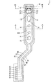
(1)サスペンション基板の構造
図1は、本発明の第1の実施の形態に係るサスペンション基板の上面図である。図1に示すように、サスペンション基板1は、金属製の長尺状の支持基板により形成されるサスペンション本体部100を備える。サスペンション本体部100の上面には、点線で示すように、書込用配線パターンW1,W2、読取用配線パターンR1,R2および熱アシスト用配線パターンH1,H2が形成されている。
(1) Structure of Suspension Board FIG. 1 is a top view of the suspension board according to the first embodiment of the present invention. As shown in FIG. 1, the
サスペンション本体部100の先端部には、U字状の開口部11を形成することにより磁気ヘッド搭載部(以下、タング部と呼ぶ)12が設けられている。タング部12は、サスペンション本体部100に対して所定の角度をなすように破線Rの箇所で折り曲げ加工される。タング部12には、矩形状の開口部13が形成される。
A magnetic head mounting portion (hereinafter referred to as a tongue portion) 12 is provided by forming a
サスペンション本体部100の一端部におけるタング部12の上面には4個の接続端子21,22,23,24が形成されている。また、サスペンション本体部100の一端部におけるタング部12の下面には2個の接続端子25,26(後述する図2参照)が形成されている。図1においては、タング部12の下面の接続端子25,26は表われていない。
Four
本実施の形態において、図示しないヘッドスライダは、上面に磁気ヘッドを有する。ヘッドスライダの下面にはレーザダイオード等の熱アシスト装置が取り付けられる。磁気ヘッドによる磁気ディスクへの情報の書込み時に、熱アシスト装置により磁気ディスクが加熱される。これにより、磁気ディスクに書き込まれる情報の密度を向上させることができる。 In the present embodiment, a head slider (not shown) has a magnetic head on the upper surface. A heat assist device such as a laser diode is attached to the lower surface of the head slider. When information is written to the magnetic disk by the magnetic head, the magnetic disk is heated by the heat assist device. Thereby, the density of information written on the magnetic disk can be improved.
タング部12の開口部13にヘッドスライダが挿入される。これにより、タング部12の上面の接続端子21〜24にヘッドスライダの上面の磁気ヘッドの端子が接続され、タング部12の下面の接続端子25,26にヘッドスライダの下面の熱アシスト装置の端子が接続される。本実施の形態において、接続端子21〜26の各々は矩形状を有する。
A head slider is inserted into the
サスペンション本体部100の他端部の上面には6個の接続端子31,32,33,34,35,36が形成されている。接続端子31〜34には、プリアンプ等の電子回路が接続される。接続端子35,36には、熱アシスト装置用の電源回路が接続される。タング部12の接続端子21〜26とサスペンション本体部100の他端部の接続端子31〜36とは、それぞれ書込用配線パターンW1,W2、読取用配線パターンR1,R2および熱アシスト用配線パターンH1,H2により電気的に接続されている。また、サスペンション本体部100には複数の孔部Hが形成されている。
Six
サスペンション基板1はハードディスク装置に設けられる。磁気ディスクへの情報の書込み時に一対の書込用配線パターンW1,W2に電流が流れる。書込用配線パターンW1と書込用配線パターンW2とは、差動の書込み信号を伝送する差動信号線路対を構成する。また、磁気ディスクからの情報の読取り時に一対の読取用配線パターンR1,R2に電流が流れる。読取用配線パターンR1と読取用配線パターンR2とは、差動の読取り信号を伝送する差動信号線路対を構成する。
The
(2)接続端子の構成
次に、サスペンション基板1の接続端子21〜26およびその周辺部分について詳細に説明する。図2は、図1のサスペンション基板1の断面図である。図2(a)は図1のサスペンション基板1のA−A線断面図を示し、図2(b)は図1のサスペンション基板1のB−B線断面図を示す。
(2) Configuration of Connection Terminal Next, the
図2(a)に示すように、例えばステンレス鋼からなる金属製の支持基板10上に例えばポリイミドからなる絶縁層41が形成されている。絶縁層41上に書込用配線パターンW1,W2、読取用配線パターンR1,R2および熱アシスト用配線パターンH1,H2が間隔をおいて平行に形成されている。
As shown in FIG. 2A, an insulating
書込用配線パターンW1,W2および熱アシスト用配線パターンH1は絶縁層41の一方の側辺に沿って延びる。熱アシスト用配線パターンH1は書込用配線パターンW1,W2の外側に配置される。読取用配線パターンR1,R2および熱アシスト用配線パターンH2は絶縁層41の他方の側辺に沿って延びる。熱アシスト用配線パターンH2は読取用配線パターンR1,R2の外側に配置される。
The write wiring patterns W1, W2 and the thermal assist wiring pattern H1 extend along one side of the insulating
書込用配線パターンW1,W2、読取用配線パターンR1,R2および熱アシスト用配線パターンH1,H2を覆うように、絶縁層41上に例えばポリイミドからなる被覆層43が形成されている。接続端子21〜24は、被覆層43から露出する。
A covering
絶縁層41の一方の側辺に沿って延びる書込用配線パターンW1,W2および熱アシスト用配線パターンH1は、図1のサスペンション本体部100の一端部で内方へ屈曲し、さらにタング部12に向かうように屈曲し、タング部12まで延びる。同様に、絶縁層41の他方の側辺に沿って延びる読取用配線パターンR1,R2および熱アシスト用配線パターンH2は、サスペンション本体部100の一端部で内方へ屈曲し、さらにタング部12に向かうように屈曲し、タング部12まで延びる。
The write wiring patterns W1, W2 and the heat assist wiring pattern H1 extending along one side of the insulating
タング部12上の書込用配線パターンW1,W2および読取用配線パターンR1,R2は、タング部12の上面の接続端子21〜24にそれぞれ接続される。タング部12上の熱アシスト用配線パターンH1,H2は、図2(b)に示すように、絶縁層41を貫通してタング部12の下面の接続端子25,26にそれぞれ接続される。接続端子25,26の表面は、絶縁層41の下面側において露出する。
The wiring patterns W1 and W2 for writing and the wiring patterns R1 and R2 for reading on the
接続端子25,26の詳細について説明する。図3は、図1のサスペンション基板1のタング部12およびその周辺の下面図である。図3に示すように、接続端子25,26は一方向に沿って延びるようにタング部12の下面に配置される。接続端子25,26の各々は、ランド部LDと直線部LNとからなる。接続端子25,26のランド部LDにはパターン接続部PCが形成され、ランド部LDとは反対側の直線部LNの端部に素子接続部ECが形成される。
Details of the
接続端子25,26のパターン接続部PCには、タング部12の上面の熱アシスト用配線パターンH1,H2がそれぞれ接続される。図3の例においては、熱アシスト用配線パターンH1,H2を容易に接続可能にするために、接続端子25,26のパターン接続部PCは接続端子25,26の他の部分よりも幅広に形成されている。したがって、接続端子25,26のパターン接続部PC間の距離は、接続端子25,26の他の部分間の距離よりも小さい。接続端子25,26の素子接続部ECには、半田によりヘッドスライダの熱アシスト装置の端子が接続される。ここで、半田の材料は、主として錫(Sn)、銀(Ag)および銅(Cu)を含む。
The heat assist wiring patterns H1 and H2 on the upper surface of the
具体的には、接続端子25は島部25aおよび金属層25bを含み、接続端子26は島部26aおよび金属層26bを含む。金属層25b,26bは、島部25a,26aよりも溶融半田の濡れ広がりが生じやすい部材により形成される。例えば、島部25a,26aはステンレス(SST)により形成され、金属層25b,26bは金(Au)により形成される。
Specifically, the
島部25a,26aは、一方向に沿って延びるようにタング部12の下面に配置される。本実施の形態においては、金属層25b,26bは、それぞれ島部25a,26aの他端部を覆うように形成される。この構成においては、島部25a,26aの一端部がパターン接続部PCとなり、島部25a,26aの他端部が素子接続部ECとなる。
The
(3)サスペンション基板の製造方法
以下、サスペンション基板1の製造方法を説明する。図4〜図6は、図1のサスペンション基板1の製造工程を示す模式図である。図4(a)〜(c)においては、左に図1のサスペンション基板1のB−B線断面図を示し、右に図1のサスペンション基板1のタング部12およびその周辺の上面図を示す。図5(a)〜図6(b)においては、左に図1のサスペンション基板1のB−B線断面図を示し、右に図1のサスペンション基板1のタング部12およびその周辺の下面図を示す。図4の上面図ならびに図5および図6の下面図には、構成の理解を容易にするために、断面図の各部材に付されたハッチングまたはドットパターンと同一のハッチングまたはドットパターンが付されている。
(3) Method for Manufacturing Suspension Board Hereinafter, a method for manufacturing the
まず、図4(a)に示すように、ステンレス鋼からなる支持層10a上に、ポリイミドからなる絶縁層41を形成する。支持層10aの厚さは、例えば10μm以上50μm以下である。絶縁層41の厚さは、例えば5μm以上15μm以下である。ここで、絶縁層41は、図1のサスペンション基板1の形状と同一の形状に形成される。また、絶縁層41に矩形状の開口部13aが形成されるとともに、複数(図4(a)の例では2個)の開口部41hが形成される。これにより、支持層10aの一部が開口部13aおよび複数の開口部41hから露出する。
First, as shown in FIG. 4A, an insulating
次に、図4(b)に示すように、絶縁層41上および開口部41hから露出する支持層10aに、所定のパターンを有する書込用配線パターンW1,W2、読取用配線パターンR1,R2および熱アシスト用配線パターンH1,H2を形成する。同時に、書込用配線パターンW1,W2および読取用配線パターンR1,R2の端部に接続端子21〜24をそれぞれ形成する。
Next, as shown in FIG. 4B, the write wiring patterns W1, W2 and the read wiring patterns R1, R2 having a predetermined pattern are formed on the insulating
書込用配線パターンW1,W2、読取用配線パターンR1,R2および熱アシスト用配線パターンH1,H2は、例えば銅からなる。本例においては、接続端子21〜24は、それぞれ書込用配線パターンW1,W2および読取用配線パターンR1,R2に順次ニッケルめっきおよび金めっきすることにより形成される。
The write wiring patterns W1, W2, the read wiring patterns R1, R2, and the thermal assist wiring patterns H1, H2 are made of, for example, copper. In the present embodiment, the
書込用配線パターンW1,W2、読取用配線パターンR1,R2および熱アシスト用配線パターンH1,H2の厚さは、例えば6μm以上18μm以下である。また、書込用配線パターンW1,W2、読取用配線パターンR1,R2および熱アシスト用配線パターンH1,H2の幅は、例えば8μm以上50μm以下である。 The thicknesses of the write wiring patterns W1, W2, the read wiring patterns R1, R2, and the thermal assist wiring patterns H1, H2 are, for example, 6 μm or more and 18 μm or less. The widths of the write wiring patterns W1, W2, the read wiring patterns R1, R2, and the thermal assist wiring patterns H1, H2 are, for example, 8 μm or more and 50 μm or less.
さらに、書込用配線パターンW1,W2間の間隔および読取用配線パターンR1,R2間の間隔は、例えばそれぞれ8μm以上100μm以下である。同様に、書込用配線パターンW1と熱アシスト用配線パターンH1との間の間隔および読取用配線パターンR2と熱アシスト用配線パターンH2との間の間隔は、例えばそれぞれ8μm以上100μm以下である。 Further, the interval between the write wiring patterns W1, W2 and the interval between the read wiring patterns R1, R2 are, for example, 8 μm or more and 100 μm or less, respectively. Similarly, the interval between the write wiring pattern W1 and the thermal assist wiring pattern H1 and the interval between the read wiring pattern R2 and the thermal assist wiring pattern H2 are, for example, 8 μm or more and 100 μm or less, respectively.
続いて、図4(c)に示すように、書込用配線パターンW1,W2、読取用配線パターンR1,R2および熱アシスト用配線パターンH1,H2を覆うように絶縁層41上にポリイミドからなる被覆層43を形成する。被覆層43の厚さは、例えば2μm以上10μm以下である。接続端子21〜24は、被覆層43から露出する。
Subsequently, as shown in FIG. 4C, the insulating
これにより、構造体1aが完成する。構造体1aにおいては、絶縁層41の一面上に書込用配線パターンW1,W2、読取用配線パターンR1,R2、熱アシスト用配線パターンH1,H2、接続端子21〜24および被覆層43が形成される。また、絶縁層41の他面上に支持層10aが形成される。
Thereby, the
次に、図5(a)に示すように、構造体1aの支持層10aの下面に例えば感光性ドライフィルムレジスト等によりレジスト膜18を形成する。続いて、図5(b)に示すように、レジスト膜18を所定のパターンで露光した後、炭酸ナトリウム等の現像液を用いて現像することによりエッチングレジスト18a,18bを形成する。
Next, as shown in FIG. 5A, a resist
ここで、エッチングレジスト18aは、図4(c)の被覆層43と重なる支持層10aの領域に形成される。また、エッチングレジスト18aは、図4(a)の絶縁層41の開口部41hおよび図4(c)の開口部13aを取り囲む矩形状の開口部18hを有する。
Here, the etching resist 18a is formed in the region of the
また、エッチングレジスト18bは、エッチングレジスト18aの開口部18h内において、絶縁層41の開口部41hに重なりかつ一方向に延びるように形成される。エッチングレジスト18bの一端部の幅は、エッチングレジスト18bの他の部分の幅よりも大きく形成される。
The etching resist 18b is formed so as to overlap the
その後、図5(c)に示すように、エッチング液として塩化第二鉄溶液および塩化第二銅溶液を用いて支持層10aをエッチングする。これにより、エッチングレジスト18a,18bから露出する支持層10aの部分が除去される。これにより、支持基板10が形成される。
Then, as shown in FIG.5 (c), the
ここで、図4(c)の開口部13aに連通するように支持基板10に矩形状の開口部13bが形成される。開口部13aと開口部13bとが連通することにより、図1および図3の開口部13が形成される。また、絶縁層41に残存する支持層10aの部分が島部25a,26aとなる。島部25a,26aはランド部および直線部を有する。島部25a,26aのランド部が図3のパターン接続部PCとなる。ランド部と反対側における島部25a,26aの直線部の端部が図3の素子接続部ECとなる。島部25a,26aのランド部は、絶縁層41の開口部41h(図4(a))を通してそれぞれ熱アシスト用配線パターンH1,H2と電気的に接続される。
Here, a
続いて、図6(a)に示すように、エッチングレジスト18a,18bを除去する。その後、図6(b)に示すように、島部25a,26aの直線部の一部をそれぞれ覆うように金属層25b,26bを形成する。金属層25b,26bの厚みは、例えば0.1μm〜3μmである。金属層25b,26bは、ニッケルおよび金(Au)を含む。本例においては、金属層25b,26bとしてニッケルめっきおよび金めっきを島部25a,26aの直線部の一部に順次形成する。
Subsequently, as shown in FIG. 6A, the etching resists 18a and 18b are removed. Thereafter, as shown in FIG. 6B, metal layers 25b and 26b are formed so as to cover part of the straight portions of the
島部25aおよび金属層25bにより接続端子25が構成され、島部26aおよび金属層26bにより接続端子26が構成される。接続端子25,26はランド部LDおよび直線部LNを有する。これにより、サスペンション基板1が完成する。
The
(4)効果
本実施の形態に係るサスペンション基板1の接続端子25においては、島部25aの素子接続部EC上に金属層25bが形成される。接続端子26においては、島部26aの素子接続部EC上に金属層26bが形成される。島部25a,26aはステンレスにより形成され、金属層25b,26bは溶融半田に対してステンレスよりも高い濡れ性を有する金めっきにより形成される。
(4) Effect In the
この構成によれば、ヘッドスライダの下面の熱アシスト装置の端子を半田により接続端子25,26に接続する場合、金属層25b,26bに塗布された溶融半田は、金属層25b,26b上で急速に広がる。その後、溶融半田は、金属層25b,26bと島部25a,26aとの境界で広がりにくくなる。そのため、溶融半田は自然放熱により冷却され、パターン接続部PCに広がる前に凝固する。これにより、簡単な構成により溶融半田の濡れ広がりを阻止することができる。
According to this configuration, when the terminals of the heat assist device on the lower surface of the head slider are connected to the
また、素子接続部ECの溶融半田がパターン接続部PCを通して他の領域に広がることが防止されるので、接続端子25,26が半田を介して意図しない他の部分(例えば隣接する接続端子のパターン接続部PC等)に電気的に接触することが防止される。その結果、溶融半田の濡れ広がりによるサスペンション基板1の信頼性の低下を抑制することができる。
Further, since the molten solder element connecting portion EC is prevented from spreading to other areas through the pattern connecting portion PC,
さらに、素子接続部ECの溶融半田がパターン接続部PCを通して他の領域に広がることが防止されるので、パターン接続部PCを接続端子25,26の素子接続部ECよりも大きく設計することができる。したがって、パターン接続部PCを熱アシスト用配線パターンH1,H2に電気的に接続することが容易になる。これにより、熱アシスト用配線パターンH1,H2および接続端子25,26をそれぞれ絶縁層41の一面および他面上に形成しつつ、熱アシスト用配線パターンH1,H2と接続端子25,26とを電気的に接続することが容易になる。
Further, since the molten solder of the element connection part EC is prevented from spreading to other regions through the pattern connection part PC, the pattern connection part PC can be designed larger than the element connection part EC of the
[2]第2の実施の形態
(1)接続端子の構成
第2の実施の形態に係るサスペンション基板1について、第1の実施の形態に係るサスペンション基板1と異なる点を説明する。第2の実施の形態に係るサスペンション基板1の構成は、接続端子25,26の構成を除いて、第1の実施の形態に係るサスペンション基板1の構成と同様である。
[2] Second Embodiment (1) Configuration of Connection Terminal A difference of the
図7は、第2の実施の形態に係るサスペンション基板1のタング部12およびその周辺の下面図である。図7に示すように、本実施の形態においては、金属層25bは、島部25aのランド部および直線部の全体を覆うように形成される。同様に、金属層26bは、島部26aのランド部および直線部の全体を覆うように形成される。
FIG. 7 is a bottom view of the
接続端子25,26の各々は、パターン接続部PCと素子接続部ECとの間に、素子接続部ECよりも幅狭に形成された幅狭部NPを有する。図7の例においては、接続端子25,26の各々の直線部の両方の側辺にV字状の切欠きが形成されることにより幅狭部NPが形成される。
Each of the
図8は、第2の実施の形態の他の例における接続端子25,26の下面図である。図8(a)の例においては、接続端子25,26の各々の直線部の両方の側辺に矩形状の切欠きが形成されることにより幅狭部NPが形成される。図8(b)の例においては、接続端子25,26の各々の直線部の両方の側辺に半円状の切欠きが形成されることにより幅狭部NPが形成される。このように、接続端子25,26の各々の直線部の両方の側辺に任意の形状の切欠きが形成されることにより幅狭部NPが形成されてもよい。
FIG. 8 is a bottom view of the
図9は、第2の実施の形態のさらに他の例における接続端子25,26の下面図である。図9(a)の例においては、接続端子25,26の各々の直線部の一方の側辺にV字状の切欠きが形成れることにより幅狭部NPが形成される。図9(b)の例においては、接続端子25,26の各々の直線部の一方の側辺に矩形状の切欠きが形成されることにより幅狭部NPが形成される。図9(c)の例においては、接続端子25,26の各々の直線部の一方の側辺に半円状の切欠きが形成されることにより幅狭部NPが形成される。このように、接続端子25,26の各々の直線部の一方の側辺に任意の形状の切欠きが形成されることにより幅狭部NPが形成されてもよい。
FIG. 9 is a bottom view of
(2)サスペンション基板の製造方法
本実施の形態におけるサスペンション基板1の製造方法は、以下の点を除いて、第1の実施の形態におけるサスペンション基板1の製造方法と同様である。
(2) Method for Manufacturing Suspension Board The method for manufacturing the
図5(b)の工程で、各エッチングレジスト18bの直線部の両方または一方の側辺に、図7〜図9の接続端子25,26の幅狭部NPに対応する切り欠きが形成される。これにより、図5(c)の工程で、島部25a,26aが形成される。
In the step of FIG. 5B, notches corresponding to the narrow portions NP of the
また、図6(b)の工程で、島部25a,26aの全体をそれぞれ覆うように金属層25b,26bを形成する。島部25a,26aの直線部上の金属層25b,26bに図7〜図9の幅狭部NPが形成される。これにより、サスペンション基板1が完成する。
In addition, in the process of FIG. 6B, metal layers 25b and 26b are formed so as to cover the
(3)効果
本実施の形態に係るサスペンション基板1においては、接続端子25,26の幅狭部NPの幅は素子接続部ECの幅およびパターン接続部PCの幅よりも小さい。そのため、幅狭部NP上での溶融半田の広がり速度は、素子接続部EC上での溶融半田の広がり速度よりも小さい。
(3) Effect In the
この場合、接続端子25,26の素子接続部ECに塗布された溶融半田は、幅狭部NP付近で滞留する。これにより、溶融半田は自然放熱により冷却され、パターン接続部PCに広がる前に凝固する。また、パターン接続部PCの幅が幅狭部NPの幅よりも大きいので、溶融半田がパターン接続部PCに広がったとしても、溶融半田はパターン接続部PCからはみ出る前に凝固する。その結果、簡単な構成により溶融半田の濡れ広がりを阻止することができる。
In this case, the molten solder applied to the element connection portion EC of the
[3]第3の実施の形態
(1)接続端子の構成
第3の実施の形態に係るサスペンション基板1について、第1の実施の形態に係るサスペンション基板1と異なる点を説明する。第3の実施の形態に係るサスペンション基板1の構成は、接続端子25,26の構成を除いて、第1の実施の形態に係るサスペンション基板1の構成と同様である。
[3] Third Embodiment (1) Configuration of Connection Terminal The
図10は、第3の実施の形態に係るサスペンション基板1のタング部12およびその周辺の下面図である。図10に示すように、本実施の形態においては、島部25a,26aの各々は、ランド部と反対側における直線部の端部に幅広部を有する。金属層25bは、島部25aのランド部、直線部および幅広部の全体を覆うように形成される。同様に、金属層26bは、島部26aの全体を覆うように形成される。それにより、接続端子25,26の各々は、ランド部LD、直線部LNおよび幅広部WPを有する。接続端子25,26の幅広部WPの幅は、直線部LNの幅よりも大きい。
FIG. 10 is a bottom view of the
接続端子25,26の幅広部WPが素子接続部ECに相当する。図10の例においては、接続端子25,26の素子接続部ECの幅はパターン接続部PCの幅と略等しく形成されるが、これに限定されない。接続端子25,26の素子接続部ECの幅は、パターン接続部PCの幅より大きく形成されてもよいし、小さく形成されてもよい。
The wide part WP of the
(2)サスペンション基板の製造方法
本実施の形態におけるサスペンション基板1の製造方法は、以下の点を除いて、第1の実施の形態におけるサスペンション基板1の製造方法と同様である。
(2) Method for Manufacturing Suspension Board The method for manufacturing the
図5(b)の工程で、エッチングレジスト18bを図10の島部25a,26aに対応する形状に形成する。これにより、図5(c)の工程で、島部25a,26aが形成される。島部25a,26aの各々は、ランド部、直線部および幅広部を有する。
5B, the etching resist 18b is formed in a shape corresponding to the
その後、図6(b)の工程で、島部25a,26aのランド部、直線部および幅広部の全体をそれぞれ覆うように金属層25b,26bを形成する。これにより、サスペンション基板1が完成する。
Thereafter, in the step of FIG. 6B, metal layers 25b and 26b are formed so as to cover the entire land, straight and wide portions of the
(3)効果
本実施の形態に係るサスペンション基板1においては、幅広部WPの幅は、幅広部WPとパターン接続部PCとの間の部分の幅よりも大きい。そのため、幅広部WPの放熱性は、幅広部WPとパターン接続部PCとの間の部分の放熱性よりも大きい。この場合、接続端子25,26の幅広部WPに塗布された溶融半田は、自然放熱により冷却され、パターン接続部PCに広がる前に凝固する。その結果、簡単な構成により溶融半田の濡れ広がりを阻止することができる。
(3) Effect In the
[4]第4の実施の形態
(1)接続端子の構成
第4の実施の形態に係るサスペンション基板1について、第1の実施の形態に係るサスペンション基板1と異なる点を説明する。第4の実施の形態に係るサスペンション基板1の構成は、接続端子25,26の構成を除いて、第1の実施の形態に係るサスペンション基板1の構成と同様である。
[4] Fourth Embodiment (1) Configuration of Connection Terminal The
図11は、第4の実施の形態に係るサスペンション基板1のタング部12およびその周辺の下面図である。図12は、図11のC−C線断面図である。図11に示すように、本実施の形態においては、金属層25bは、島部25aのランド部および直線部の全体を覆うように形成される。同様に、金属層26bは、島部26aのランド部および直線部の全体を覆うように形成される。
FIG. 11 is a bottom view of the
本実施の形態の接続端子25,26においては、ランド部LDと反対側における直線部LNの端部が素子接続部ECに相当する。図12に示すように、接続端子25の素子接続部ECの厚みは、接続端子25の他の部分の厚みよりも大きく形成される。同様に、接続端子26の素子接続部ECの厚みは、接続端子26の他の部分の厚みよりも大きく形成される。
In the
図13は、第4の実施の形態の他の例に係るサスペンション基板1の断面図である。図13は、図11のC−C線断面図に相当する。図13の例においては、接続端子25の素子接続部ECの厚みが、接続端子25の他の部分の厚みよりも小さく形成される。同様に、接続端子26の素子接続部ECの厚みが、接続端子26の他の部分の厚みよりも小さく形成される。このように、接続端子25,26の素子接続部ECの厚みは、接続端子25,26の他の部分の厚みよりも大きく形成されてもよいし、小さく形成されてもよい。
FIG. 13 is a cross-sectional view of a
(2)サスペンション基板の製造方法
本実施の形態におけるサスペンション基板1の製造方法は、以下の点を除いて、第1の実施の形態におけるサスペンション基板1の製造方法と同様である。
(2) Method for Manufacturing Suspension Board The method for manufacturing the
図6(a)の工程の後、島部25a,26aの一部にエッチングレジストを形成し、エッチング液として塩化第二鉄溶液および塩化第二銅溶液を用いてエッチングレジストから露出する島部25a,26aの部分をハーフエッチングする。ここで、ランド部と反対側における直線部の端部がハーフエッチングされてもよい。あるいは、ランド部と反対側における直線部の端部を除く直線部がハーフエッチングされてもよい。ハーフエッチングされた島部25a,26aの部分の厚みは、島部25a,26aの他の部分よりも小さくなる。
After the step of FIG. 6A, an etching resist is formed on a part of the
その後、図6(b)の工程で、島部25a,26aのランド部および直線部の全体をそれぞれ覆うように金属層25b,26bを形成する。これにより、サスペンション基板1が完成する。
Thereafter, in the step of FIG. 6B, metal layers 25b and 26b are formed so as to cover the entire land portions and straight portions of the
(3)効果
本実施の形態に係るサスペンション基板1においては、接続端子25,26の素子接続部ECに塗布された溶融半田は、素子接続部EC上で広がる。その後、溶融半田は、素子接続部ECの縁に沿って下方または上方に広がる際に自然放熱により冷却され、パターン接続部PCに広がる前に凝固する。これにより、簡単な構成により溶融半田の濡れ広がりを阻止することができる。
(3) Effect In the
[5]第5の実施の形態
(1)接続端子の構成
第5の実施の形態に係るサスペンション基板1について、第1の実施の形態に係るサスペンション基板1と異なる点を説明する。第5の実施の形態に係るサスペンション基板1の構成は、接続端子25,26の構成を除いて、第1の実施の形態に係るサスペンション基板1の構成と同様である。
[5] Fifth Embodiment (1) Configuration of Connection Terminal The
図14は、第5の実施の形態に係るサスペンション基板1のタング部12およびその周辺の下面図である。図15は、図14のD−D線断面図である。図14および図15に示すように、本実施の形態においては、接続端子25は樹脂層25cをさらに含み、接続端子26は樹脂層26cをさらに含む。
FIG. 14 is a bottom view of the
本実施の形態においては、樹脂層25cは島部25aのランド部と反対側の直線部の端部を除く直線部を覆うように設けられ、樹脂層26cは島部26aのランド部と反対側の直線部の端部を除く直線部を覆うように設けられる。樹脂層25cから露出する島部25aの直線部の端部を覆うように金属層25bが形成され、樹脂層26cから露出する島部26aの直線部の端部を覆うように金属層26bが形成される。
In the present embodiment, the
図15に示すように、島部25a上の樹脂層25cの厚みは、島部25a上の金属層25bの厚みよりも大きい。樹脂層25c上には金属層25bは形成されない。同様に、島部26a上の樹脂層26cの厚みは、島部26a上の金属層26bの厚みよりも大きい。樹脂層26c上には金属層26bは形成されない。
As shown in FIG. 15, the thickness of the
(2)サスペンション基板の製造方法
本実施の形態におけるサスペンション基板1の製造方法は、以下の点を除いて、第1の実施の形態におけるサスペンション基板1の製造方法と同様である。
(2) Method for Manufacturing Suspension Board The method for manufacturing the
図6(a)の工程の後、島部25aのランド部と反対側の直線部の端部を除く直線部を覆うように樹脂層25cを形成するとともに、島部26aのランド部と反対側の直線部の端部を除く直線部を覆うように樹脂層26cを形成する。本例においては、樹脂層25c,26cはポリイミドにより形成される。
After the step of FIG. 6A, the
島部25a,26a上の樹脂層25c,26cの厚みは、2μm以上6μm以下であることが好ましい。これにより、サスペンション基板1が大型化することを抑制しつつ、接続端子25,26の素子接続部ECに塗布された溶融半田が樹脂層25c,26cを越えて接続端子25,26のパターン接続部PCまで広がることを確実に防止することができる。
The thickness of the resin layers 25c and 26c on the
その後、図6(b)の工程で、樹脂層25cから露出する島部25aの直線部の端部を覆うように金属層25bを形成し、樹脂層26cから露出する島部26aの直線部の端部を覆うように金属層26bを形成する。これにより、サスペンション基板1が完成する。
6B, a
(3)効果
本実施の形態に係るサスペンション基板1においては、接続端子25,26の素子接続部ECに塗布された溶融半田は、素子接続部EC上で広がった後、樹脂層25c,26cによりせき止められる。これにより、溶融半田はパターン接続部PCに広がる前に凝固する。その結果、簡単な構成により溶融半田の濡れ広がりを阻止することができる。
(3) Effect In the
[6]第6の実施の形態
(1)接続端子の構成
第6の実施の形態に係るサスペンション基板1について、第1の実施の形態に係るサスペンション基板1と異なる点を説明する。第6の実施の形態に係るサスペンション基板1の構成は、接続端子25,26の構成を除いて、第1の実施の形態に係るサスペンション基板1の構成と同様である。
[6] Sixth Embodiment (1) Configuration of Connection Terminal The
図16は、第6の実施の形態に係るサスペンション基板1のタング部12およびその周辺の下面図である。図17は、図16のE−E線断面図である。図16および図17に示すように、本実施の形態においては、接続端子25は金属層25dをさらに含み、接続端子26は金属層26dをさらに含む。
FIG. 16 is a bottom view of the
金属層25dは島部25aのランド部と反対側の直線部の端部を除く直線部を覆うように設けられ、金属層26dは島部26aのランド部と反対側の直線部の端部を除く直線部を覆うように設けられる。島部25aおよび金属層25dの全体を覆うように金属層25bが形成され、島部26aおよび金属層26dの全体を覆うように金属層26bが形成される。
The
図18は、第6の実施の形態の他の例に係るサスペンション基板1の断面図である。図18(a),(b)は、図16のE−E線断面図に相当する。図18(a)の例においては、島部25aのランド部と反対側の直線部の端部に金属層25dが形成される。同様に、島部26aのランド部と反対側の直線部の端部に金属層26dが形成される。島部25aおよび金属層25dの全体を覆うように金属層25bが形成され、島部26aおよび金属層26dの全体を覆うように金属層26bが形成される。
FIG. 18 is a cross-sectional view of a
図18(b)の例においては、島部25aのランド部と反対側の直線部の端部を除く部分に金属層25dが形成される。同様に、島部26aのランド部と反対側の直線部の端部を除く部分に金属層26dが形成される。島部25aおよび金属層25dの全体を覆うように金属層25bが形成され、島部26aおよび金属層26dの全体を覆うように金属層26bが形成される。
In the example of FIG. 18B, the
(2)サスペンション基板の製造方法
本実施の形態におけるサスペンション基板1の製造方法は、以下の点を除いて、第1の実施の形態におけるサスペンション基板1の製造方法と同様である。
(2) Method for Manufacturing Suspension Board The method for manufacturing the
図6(a)の工程の後、島部25aの一部を覆うように金属層25dを形成するとともに、島部26aの一部を覆うように金属層26dを形成する。本例においては、金属層25d,26dは銅により形成される。
After the step of FIG. 6A, the
その後、図6(b)の工程で、島部25aおよび金属層25dの全体を覆うように金属層25bを形成し、島部26aおよび金属層26dの全体を覆うように金属層25bを形成する。これにより、サスペンション基板1が完成する。
6B, the
(3)効果
本実施の形態に係るサスペンション基板1においては、接続端子25,26の素子接続部ECに塗布された溶融半田は、素子接続部EC上で広がった後、金属層25d,26dによりせき止められる。あるいは、金属層25d,26dの放熱性が大きいので、接続端子25,26の素子接続部ECに塗布された溶融半田は、金属層25d,26dの縁に沿って下方または上方に広がる際に自然放熱により冷却される。これらにより、溶融半田はパターン接続部PCに広がる前に凝固する。その結果、簡単な構成により溶融半田の濡れ広がりを阻止することができる。
(3) Effect In the
[7]請求項の各構成要素と実施の形態の各部との対応関係
以下、請求項の各構成要素と実施の形態の各部との対応の例について説明するが、本発明は下記の例に限定されない。
[7] Correspondence relationship between each constituent element of claim and each part of embodiment The following describes an example of the correspondence between each constituent element of the claim and each part of the embodiment. It is not limited.
サスペンション基板1が回路付きサスペンション基板の例であり、絶縁層41が絶縁層の例であり、熱アシスト用配線パターンH1,H2が導体層の例であり、支持基板10が支持基板の例である。接続端子25,26が接続端子の例であり、素子接続部ECが第1の部分の例であり、パターン接続部PCが第2の部分の例であり、金属層25b,26bが表面処理層の例である。幅狭部NPが幅狭部の例であり、幅広部WPが幅広部の例であり、樹脂層25c,26cまたは金属層25d,26dが突起部の例であり、支持層10aが支持層の例であり、構造体1aが構造体の例である。
The
第1の実施の形態においては、金属層25b,26bが広がり阻止部の例である。第2の実施の形態においては、幅狭部NPが幅変化部および広がり阻止部の例である。第3の実施の形態においては、接続端子25,26の直線部LNと幅広部WPとの境界が幅変化部および広がり阻止部の例である。第4の実施の形態においては、接続端子25,26の素子接続部ECと他の部分との境界が厚み変化部および広がり阻止部の例である。第5の実施の形態においては、樹脂層25c,26cが厚み変化部および広がり阻止部の例である。第6の実施の形態においては、金属層25d,26dが厚み変化部および広がり阻止部の例である。
In the first embodiment, the metal layers 25b and 26b are an example of spread preventing portions. In the second embodiment, the narrow portion NP is an example of the width changing portion and the spread preventing portion. In the third embodiment, the boundary between the straight portion LN of the
請求項の各構成要素として、請求項に記載されている構成または機能を有する他の種々の要素を用いることもできる。
[8]参考形態
(1)第1の参考形態に係る回路付きサスペンション基板は、半田により回路素子が接続される回路付きサスペンション基板であって、第1および第2の面を有する絶縁層と、絶縁層の第1の面上に形成される導体層と、絶縁層の第2の面上に形成される導電性の支持基板と、絶縁層の第2の面上に形成され、支持基板から電気的に絶縁されかつ導体層に電気的に接続される接続端子とを備え、接続端子は、第1および第2の部分を有するとともに、第1の部分に塗布された溶融半田が第2の部分に広がることを阻止する広がり阻止部を有するものである。
この回路付きサスペンション基板においては、絶縁層の第1および第2の面上にそれぞれ導体層および導電性の支持基板が形成される。また、絶縁層の第2の面上に支持基板から電気的に絶縁されかつ導体層に電気的に接続される接続端子が形成される。接続端子は、第1の部分、第2の部分および広がり阻止部を有する。
この構成によれば、半田により回路素子を接続端子の第1の部分に接続する場合、第1の部分に塗布された溶融半田が第2の部分に広がることが広がり阻止部により阻止される。これにより、第2の部分が半田を介して意図しない他の部分に電気的に接触することが防止される。その結果、溶融半田の濡れ広がりによる回路付きサスペンション基板の信頼性の低下を抑制することができる。
(2)広がり阻止部は、第1の部分の表面上に形成された表面処理層であり、表面処理層の材料は、溶融半田に対して第2の部分の表面の材料よりも高い濡れ性を有してもよい。
この場合、接続端子の第1の部分上の表面処理層に塗布された溶融半田は、表面処理層上で急速に広がった後、表面処理層と第2の部分との境界で広がりにくくなる。これにより、溶融半田は自然放熱により冷却され、第2の部分に広がる前に凝固する。その結果、簡単な構成により溶融半田の濡れ広がりを阻止することができる。
(3)第1および第2の部分はステンレスにより形成され、表面処理層は金めっきにより形成されてもよい。この場合、表面処理層と第2の部分との境界で溶融半田の濡れ広がりを十分に阻止することができる。
(4)接続端子は、第1の部分と第2の部分との間で幅が変化する幅変化部を有し、広がり阻止部は幅変化部であってもよい。
この場合、接続端子の第1の部分に塗布された溶融半田は、幅変化部を通過する際に自然放熱により冷却され、第2の部分に広がる前に凝固する。これにより、簡単な構成により溶融半田の濡れ広がりを阻止することができる。
(5)幅変化部は、第1の部分の幅および第2の部分の幅よりも小さい幅を有する幅狭部を含んでもよい。
この場合、幅狭部の幅は第1の部分の幅および第2の部分の幅よりも小さいので、幅狭部上での溶融半田の広がり速度は、第1の部分上での溶融半田の広がり速度よりも小さい。そのため、接続端子の第1の部分に塗布された溶融半田は、幅狭部付近で滞留する。これにより、溶融半田は自然放熱により冷却され、第2の部分に広がる前に凝固する。また、第2の部分の幅が幅変化部の幅よりも大きいので、溶融半田が第2の部分に広がったとしても、溶融半田は第2の部分からはみ出る前に凝固する。その結果、簡単な構成により溶融半田の濡れ広がりを阻止することができる。
(6)第1の部分は、第2の部分の幅よりも大きい幅を有する幅広部からなり、幅変化部は、幅広部と第2の部分との境界であってもよい。
この場合、幅広部の幅は、第2の部分の幅よりも大きいので、幅広部の放熱性は、第2の部分の放熱性よりも大きい。そのため、接続端子の第1の部分に塗布された溶融半田は、自然放熱により冷却され、第2の部分に広がる前に凝固する。その結果、簡単な構成により溶融半田の濡れ広がりを阻止することができる。
(7)接続端子は、第1の部分と第2の部分との間で厚みが変化する厚み変化部を有し、広がり阻止部は厚み変化部であってもよい。
この場合、接続端子の第1の部分に塗布された溶融半田は、厚み変化部を通過する際に自然放熱により冷却され、第2の部分に広がる前に凝固する。これにより、簡単な構成により溶融半田の濡れ広がりを阻止することができる。
(8)第1の部分は第2の部分よりも大きい厚みを有し、厚み変化部は第1の部分と第2の部分との境界であってもよい。
この場合、接続端子の第1の部分に塗布された溶融半田は、第1の部分上で広がった後、第1の部分の縁に沿って下方に広がる際に自然放熱により冷却され、第2の部分に広がる前に凝固する。これにより、簡単な構成により溶融半田の濡れ広がりを阻止することができる。
(9)第2の部分は第1の部分よりも大きい厚みを有し、厚み変化部は第1の部分と第2の部分との境界であってもよい。
この場合、接続端子の第1の部分に塗布された溶融半田は、第1の部分上で広がった後、第2の部分の縁によりせき止められる。あるいは、接続端子の第1の部分に塗布された溶融半田は、第2の部分の縁に沿って上方に広がる際に自然放熱により冷却される。これらにより、溶融半田は第2の部分に広がる前に凝固する。その結果、簡単な構成により溶融半田の濡れ広がりを阻止することができる。
(10)厚み変化部は、第1の部分と第2の部分との境界に沿って設けられる突起部であり、突起部は、第1および第2の部分の表面から突出するように形成されてもよい。
この場合、接続端子の第1の部分に塗布された溶融半田は、第1の部分上で広がった後、突起部によりせき止められる。あるいは、接続端子の第1の部分に塗布された溶融半田は、突起部の縁に沿って上方に広がる際に自然放熱により冷却される。これらにより、溶融半田は第2の部分に広がる前に凝固する。その結果、簡単な構成により溶融半田の濡れ広がりを阻止することができる。
(11)突起部は樹脂により形成されてもよい。この場合、接続端子の第1の部分と第2の部分との間の表面上に容易に突起部を形成することができる。
(12)突起部は金属により形成されてもよい。この場合、突起部での放熱性が向上する。これにより、簡単な構成により溶融半田の濡れ広がりを阻止することができる。
(13)第2の参考形態に係る回路付きサスペンション基板の製造方法は、半田により回路素子が接続される回路付きサスペンション基板の製造方法であって、第1および第2の面を有する絶縁層、絶縁層の第1の面上に形成される導体層および絶縁層の第2の面上に形成される導電性の支持層を含む構造体を準備する工程と、支持層を加工することにより絶縁層の第2の面上に導電性の支持基板を形成する工程と、支持層を加工することにより絶縁層の第2の面上に支持基板から電気的に絶縁されかつ導体層に電気的に接続される接続端子を形成する工程とを含み、接続端子は、第1および第2の部分を有するとともに、第1の部分に塗布された溶融半田が第2の部分に広がることを阻止する広がり阻止部を有するものである。
この回路付きサスペンション基板の製造方法においては、絶縁層の第1および第2の面上にそれぞれ導体層および導電性の支持層が形成される。支持層が加工されることにより、絶縁層の第2の面上に導電性の支持層が形成され、支持基板から電気的に絶縁されかつ導体層に電気的に接続される接続端子が形成される。接続端子は、第1の部分、第2の部分および広がり阻止部を有する。
この構成によれば、半田により回路素子を接続端子の第1の部分に接続する場合、第1の部分に塗布された溶融半田が第2の部分に広がることが広がり阻止部により阻止される。これにより、第2の部分が半田を介して意図しない他の部分に電気的に接触することが防止される。その結果、溶融半田の濡れ広がりによる回路付きサスペンション基板の信頼性の低下を抑制することができる。
As each constituent element in the claims, various other elements having configurations or functions described in the claims can be used.
[8] Reference form
(1) A suspension board with circuit according to a first embodiment is a suspension board with circuit to which circuit elements are connected by solder, an insulating layer having first and second surfaces, and a first insulating layer. A conductive layer formed on the surface of the insulating layer, a conductive support substrate formed on the second surface of the insulating layer, and formed on the second surface of the insulating layer and electrically insulated from the support substrate. And a connection terminal electrically connected to the conductor layer, the connection terminal having first and second portions, and that the molten solder applied to the first portion spreads to the second portion. It has a spread blocking part to block.
In this suspension board with circuit, a conductor layer and a conductive support board are formed on the first and second surfaces of the insulating layer, respectively. In addition, a connection terminal that is electrically insulated from the support substrate and electrically connected to the conductor layer is formed on the second surface of the insulating layer. The connection terminal has a first portion, a second portion, and a spread preventing portion.
According to this configuration, when the circuit element is connected to the first portion of the connection terminal by the solder, the molten solder applied to the first portion spreads to the second portion and is prevented by the spreading preventing portion. This prevents the second portion from being in electrical contact with other unintended portions via the solder. As a result, it is possible to suppress a decrease in the reliability of the suspension board with circuit due to the wet spreading of the molten solder.
(2) The spread preventing portion is a surface treatment layer formed on the surface of the first portion, and the material of the surface treatment layer has higher wettability with respect to molten solder than the material of the surface of the second portion. You may have.
In this case, the molten solder applied to the surface treatment layer on the first portion of the connection terminal spreads rapidly on the surface treatment layer and then hardly spreads at the boundary between the surface treatment layer and the second portion. As a result, the molten solder is cooled by natural heat dissipation and solidifies before spreading to the second portion. As a result, it is possible to prevent wet solder from spreading by a simple configuration.
(3) The first and second portions may be formed of stainless steel, and the surface treatment layer may be formed of gold plating. In this case, wetting and spreading of the molten solder can be sufficiently prevented at the boundary between the surface treatment layer and the second portion.
(4) The connection terminal may include a width change portion whose width changes between the first portion and the second portion, and the spread prevention portion may be a width change portion.
In this case, the molten solder applied to the first portion of the connection terminal is cooled by natural heat dissipation when passing through the width change portion, and solidifies before spreading to the second portion. Thereby, wetting spread of the molten solder can be prevented with a simple configuration.
(5) The width changing portion may include a narrow portion having a width smaller than the width of the first portion and the width of the second portion.
In this case, since the width of the narrow portion is smaller than the width of the first portion and the width of the second portion, the spreading speed of the molten solder on the narrow portion is the speed of the molten solder on the first portion. Less than spreading speed. Therefore, the molten solder applied to the first portion of the connection terminal stays near the narrow portion. As a result, the molten solder is cooled by natural heat dissipation and solidifies before spreading to the second portion. In addition, since the width of the second portion is larger than the width of the width changing portion, even if the molten solder spreads to the second portion, the molten solder solidifies before protruding from the second portion. As a result, it is possible to prevent wet solder from spreading by a simple configuration.
(6) The first portion may be a wide portion having a width larger than that of the second portion, and the width changing portion may be a boundary between the wide portion and the second portion.
In this case, since the width of the wide portion is larger than the width of the second portion, the heat dissipation performance of the wide portion is greater than the heat dissipation performance of the second portion. Therefore, the molten solder applied to the first portion of the connection terminal is cooled by natural heat dissipation and solidifies before spreading to the second portion. As a result, it is possible to prevent wet solder from spreading by a simple configuration.
(7) The connection terminal may include a thickness changing portion whose thickness changes between the first portion and the second portion, and the spread preventing portion may be a thickness changing portion.
In this case, the molten solder applied to the first portion of the connection terminal is cooled by natural heat dissipation when passing through the thickness changing portion, and solidifies before spreading to the second portion. Thereby, wetting spread of the molten solder can be prevented with a simple configuration.
(8) The first portion may have a thickness greater than that of the second portion, and the thickness changing portion may be a boundary between the first portion and the second portion.
In this case, the molten solder applied to the first portion of the connection terminal spreads on the first portion, and then is cooled by natural heat dissipation when spreading downward along the edge of the first portion. It solidifies before spreading to the part. Thereby, wetting spread of the molten solder can be prevented with a simple configuration.
(9) The second portion may have a thickness larger than that of the first portion, and the thickness changing portion may be a boundary between the first portion and the second portion.
In this case, the molten solder applied to the first portion of the connection terminal spreads on the first portion and is then blocked by the edge of the second portion. Alternatively, the molten solder applied to the first portion of the connection terminal is cooled by natural heat dissipation when spreading upward along the edge of the second portion. As a result, the molten solder solidifies before spreading to the second portion. As a result, it is possible to prevent wet solder from spreading by a simple configuration.
(10) The thickness changing portion is a protrusion provided along the boundary between the first portion and the second portion, and the protrusion is formed so as to protrude from the surfaces of the first and second portions. May be.
In this case, the molten solder applied to the first portion of the connection terminal spreads on the first portion and is then blocked by the protrusion. Alternatively, the molten solder applied to the first portion of the connection terminal is cooled by natural heat dissipation when spreading upward along the edge of the protrusion. As a result, the molten solder solidifies before spreading to the second portion. As a result, it is possible to prevent wet solder from spreading by a simple configuration.
(11) The protrusion may be made of resin. In this case, the protrusion can be easily formed on the surface between the first portion and the second portion of the connection terminal.
(12) The protrusion may be made of metal. In this case, the heat dissipation at the protrusion is improved. Thereby, wetting spread of the molten solder can be prevented with a simple configuration.
(13) A method for manufacturing a suspension board with circuit according to a second embodiment is a method for manufacturing a suspension board with circuit in which circuit elements are connected by solder, and includes an insulating layer having first and second surfaces, Providing a structure including a conductive layer formed on the first surface of the insulating layer and a conductive support layer formed on the second surface of the insulating layer; and insulating by processing the support layer Forming a conductive support substrate on the second surface of the layer and processing the support layer to electrically insulate the support layer on the second surface of the insulating layer and electrically Forming a connection terminal to be connected, the connection terminal having first and second portions, and a spread for preventing the molten solder applied to the first portion from spreading to the second portion It has a blocking part.
In this method of manufacturing a suspension board with circuit, a conductor layer and a conductive support layer are formed on the first and second surfaces of the insulating layer, respectively. By processing the support layer, a conductive support layer is formed on the second surface of the insulating layer, and a connection terminal that is electrically insulated from the support substrate and electrically connected to the conductor layer is formed. The The connection terminal has a first portion, a second portion, and a spread preventing portion.
According to this configuration, when the circuit element is connected to the first portion of the connection terminal by the solder, the molten solder applied to the first portion spreads to the second portion and is prevented by the spreading preventing portion. This prevents the second portion from being in electrical contact with other unintended portions via the solder. As a result, it is possible to suppress a decrease in the reliability of the suspension board with circuit due to the wet spreading of the molten solder.
本発明は、種々の接続端子を有する配線回路基板または電気機器等に有効に利用することができる。 INDUSTRIAL APPLICABILITY The present invention can be effectively used for a printed circuit board having various connection terminals or an electric device.
1 サスペンション基板
1a 構造体
10 支持基板
10a 支持層
11,13,13a,13b,18h,41h 開口部
12 タング部
18 レジスト膜
18a,18b エッチングレジスト
21〜26,31〜36 接続端子
25a,26a 島部
25b,25d,26b,26d 金属層
25c,26c 樹脂層
41 絶縁層
43 被覆層
100 サスペンション本体部
EC 素子接続部
H 孔部
H1,H2 熱アシスト用配線パターン
LD ランド部
LN 直線部
NP 幅狭部
PC パターン接続部
R1,R2 読取用配線パターン
W1,W2 書込用配線パターン
WP 幅広部
DESCRIPTION OF
Claims (13)
第1および第2の面を有する絶縁層と、
前記絶縁層の前記第1の面上に形成される導体層と、
前記絶縁層の前記第2の面上に形成される導電性の支持基板と、
前記絶縁層の前記第2の面上に形成され、前記支持基板から電気的に絶縁されかつ前記導体層に電気的に接続される接続端子とを備え、
前記接続端子は、第1および第2の部分を有するとともに、前記第1の部分に塗布された半田が前記第2の部分に広がることを阻止する広がり阻止部を有し、
前記接続端子は、前記絶縁層に接する第3の面と、前記第3の面とは反対側の第4の面とを有し、
前記第4の面は、前記第1の部分および前記第2の部分を有する、回路付きサスペンション基板。 A suspension board with a circuit to which circuit elements are connected by solder,
An insulating layer having first and second surfaces;
A conductor layer formed on the first surface of the insulating layer;
A conductive support substrate formed on the second surface of the insulating layer;
A connection terminal formed on the second surface of the insulating layer, electrically insulated from the support substrate and electrically connected to the conductor layer;
The connection terminal has a first and second portion, the solder applied to the first portion have a spread preventing portion that prevents the spread the second portion,
The connection terminal has a third surface in contact with the insulating layer, and a fourth surface opposite to the third surface,
The fourth surface, the chromatic said first portion and said second portion, suspension board with a circuit.
前記表面処理層の材料は、溶融半田に対して前記第2の部分の表面の材料よりも高い濡れ性を有する、請求項1記載の回路付きサスペンション基板。 The spread prevention part is a surface treatment layer formed on the surface of the first part,
The suspension board with circuit according to claim 1, wherein a material of the surface treatment layer has higher wettability with respect to molten solder than a material of a surface of the second portion.
前記広がり阻止部は前記幅変化部である、請求項1記載の回路付きサスペンション基板。 The connection terminal has a width changing portion whose width changes between the first portion and the second portion,
The suspension board with circuit according to claim 1, wherein the spread preventing portion is the width changing portion.
前記幅変化部は、前記幅広部と前記第2の部分との境界である、請求項4記載の回路付きサスペンション基板。 The first portion comprises a wide portion having a width greater than the width of the second portion,
The suspension board with circuit according to claim 4, wherein the width changing portion is a boundary between the wide portion and the second portion.
前記広がり阻止部は前記厚み変化部である、請求項1記載の回路付きサスペンション基板。 The connection terminal has a thickness changing portion whose thickness changes between the first portion and the second portion,
The suspension board with circuit according to claim 1, wherein the spread preventing portion is the thickness changing portion.
前記突起部は、前記第1および第2の部分の表面から突出するように形成される、請求項7記載の回路付きサスペンション基板。 The thickness changing part is a protrusion provided along a boundary between the first part and the second part,
The suspension board with circuit according to claim 7, wherein the protrusion is formed so as to protrude from surfaces of the first and second portions.
第1および第2の面を有する絶縁層、前記絶縁層の前記第1の面上に形成される導体層および前記絶縁層の前記第2の面上に形成される導電性の支持層を含む構造体を準備する工程と、
前記支持層を加工することにより前記絶縁層の第2の面上に導電性の支持基板を形成する工程と、
前記支持層を加工することにより前記絶縁層の第2の面上に前記支持基板から電気的に絶縁されかつ前記導体層に電気的に接続される接続端子を形成する工程とを含み、
前記接続端子は、第1および第2の部分を有するとともに、前記第1の部分に塗布された半田が前記第2の部分に広がることを阻止する広がり阻止部を有し、
前記接続端子は、前記絶縁層に接する第3の面と、前記第3の面とは反対側の第4の面とを有し、
前記第4の面は、前記第1の部分および前記第2の部分を有する、回路付きサスペンション基板の製造方法。 A method of manufacturing a suspension board with a circuit to which circuit elements are connected by solder,
An insulating layer having first and second surfaces; a conductor layer formed on the first surface of the insulating layer; and a conductive support layer formed on the second surface of the insulating layer. Preparing the structure;
Forming a conductive support substrate on the second surface of the insulating layer by processing the support layer;
Forming a connection terminal electrically insulated from the support substrate and electrically connected to the conductor layer on the second surface of the insulating layer by processing the support layer;
The connection terminal has a first and second portion, the solder applied to the first portion have a spread preventing portion that prevents the spread the second portion,
The connection terminal has a third surface in contact with the insulating layer, and a fourth surface opposite to the third surface,
The fourth surface, the chromatic said first portion and said second portion, the manufacturing method of the suspension board with a circuit.
Priority Applications (3)
| Application Number | Priority Date | Filing Date | Title |
|---|---|---|---|
| JP2013107829A JP6101151B2 (en) | 2013-05-22 | 2013-05-22 | Suspension board with circuit and manufacturing method thereof |
| US14/273,657 US9763334B2 (en) | 2013-05-22 | 2014-05-09 | Suspension board with circuit and method of manufacturing the same |
| CN201410219489.1A CN104183247B (en) | 2013-05-22 | 2014-05-22 | Hanging base board and its manufacturing method with circuit |
Applications Claiming Priority (1)
| Application Number | Priority Date | Filing Date | Title |
|---|---|---|---|
| JP2013107829A JP6101151B2 (en) | 2013-05-22 | 2013-05-22 | Suspension board with circuit and manufacturing method thereof |
Publications (2)
| Publication Number | Publication Date |
|---|---|
| JP2014229330A JP2014229330A (en) | 2014-12-08 |
| JP6101151B2 true JP6101151B2 (en) | 2017-03-22 |
Family
ID=51934619
Family Applications (1)
| Application Number | Title | Priority Date | Filing Date |
|---|---|---|---|
| JP2013107829A Active JP6101151B2 (en) | 2013-05-22 | 2013-05-22 | Suspension board with circuit and manufacturing method thereof |
Country Status (3)
| Country | Link |
|---|---|
| US (1) | US9763334B2 (en) |
| JP (1) | JP6101151B2 (en) |
| CN (1) | CN104183247B (en) |
Families Citing this family (6)
| Publication number | Priority date | Publication date | Assignee | Title |
|---|---|---|---|---|
| JP6072366B1 (en) * | 2015-03-10 | 2017-02-01 | オリンパス株式会社 | Endoscopic imaging device |
| US9940957B2 (en) * | 2015-07-31 | 2018-04-10 | Nitto Denko Corporation | Printed circuit board and method of manufacturing the same |
| JP6807180B2 (en) * | 2015-07-31 | 2021-01-06 | 日東電工株式会社 | Wiring circuit board and its manufacturing method |
| JP6802688B2 (en) * | 2016-11-02 | 2020-12-16 | 日東電工株式会社 | Wiring circuit board |
| US11091850B2 (en) * | 2017-01-23 | 2021-08-17 | Nitto Denko Corporation | Producing method of wired circuit board |
| EP3367383B1 (en) | 2017-02-23 | 2023-12-20 | Nokia Technologies Oy | Virtual reality |
Family Cites Families (18)
| Publication number | Priority date | Publication date | Assignee | Title |
|---|---|---|---|---|
| JPH0632367B2 (en) * | 1989-01-24 | 1994-04-27 | 富士通株式会社 | Method for forming I / O pad of ceramic substrate |
| US5041901A (en) * | 1989-05-10 | 1991-08-20 | Hitachi, Ltd. | Lead frame and semiconductor device using the same |
| US5194137A (en) * | 1991-08-05 | 1993-03-16 | Motorola Inc. | Solder plate reflow method for forming solder-bumped terminals |
| US6300678B1 (en) * | 1997-10-03 | 2001-10-09 | Fujitsu Limited | I/O pin having solder dam for connecting substrates |
| JPH11167944A (en) * | 1997-10-03 | 1999-06-22 | Fujitsu Ltd | I/o pin with solder dam for connecting boards |
| JP2001209918A (en) * | 1999-11-19 | 2001-08-03 | Nitto Denko Corp | Suspension substrate with circuit |
| US6485843B1 (en) * | 2000-09-29 | 2002-11-26 | Altera Corporation | Apparatus and method for mounting BGA devices |
| JP4923336B2 (en) * | 2001-04-10 | 2012-04-25 | 日本電気株式会社 | Circuit board and electronic device using the circuit board |
| JP3692314B2 (en) * | 2001-07-17 | 2005-09-07 | 日東電工株式会社 | Printed circuit board |
| JP4222882B2 (en) * | 2003-06-03 | 2009-02-12 | 日東電工株式会社 | Printed circuit board |
| JP5395625B2 (en) * | 2009-11-11 | 2014-01-22 | 日東電工株式会社 | Wiring circuit board and fuel cell |
| JP4962879B2 (en) * | 2010-07-06 | 2012-06-27 | 大日本印刷株式会社 | Suspension board, suspension, suspension with head, and hard disk drive |
| JP4977906B2 (en) * | 2010-07-15 | 2012-07-18 | 大日本印刷株式会社 | Suspension substrate, suspension, suspension with head, hard disk drive, suspension substrate manufacturing method, and suspension continuity inspection method |
| US8208227B2 (en) * | 2010-10-12 | 2012-06-26 | Nitto Denko Corporation | Suspension board with circuit and producing method thereof |
| JP5603744B2 (en) * | 2010-11-10 | 2014-10-08 | 日東電工株式会社 | Suspension board with circuit and manufacturing method thereof |
| JP5711947B2 (en) | 2010-11-30 | 2015-05-07 | 日本発條株式会社 | Flexure for disk unit |
| JP5045831B2 (en) | 2011-03-08 | 2012-10-10 | 大日本印刷株式会社 | Flexure substrate for suspension and manufacturing method thereof |
| JP6114489B2 (en) * | 2011-05-11 | 2017-04-12 | 大日本印刷株式会社 | Suspension board, suspension, suspension with element, and hard disk drive |
-
2013
- 2013-05-22 JP JP2013107829A patent/JP6101151B2/en active Active
-
2014
- 2014-05-09 US US14/273,657 patent/US9763334B2/en active Active
- 2014-05-22 CN CN201410219489.1A patent/CN104183247B/en active Active
Also Published As
| Publication number | Publication date |
|---|---|
| CN104183247B (en) | 2019-03-08 |
| US9763334B2 (en) | 2017-09-12 |
| JP2014229330A (en) | 2014-12-08 |
| CN104183247A (en) | 2014-12-03 |
| US20140345920A1 (en) | 2014-11-27 |
Similar Documents
| Publication | Publication Date | Title |
|---|---|---|
| JP6101151B2 (en) | Suspension board with circuit and manufacturing method thereof | |
| JP2009129490A (en) | Wired circuit board | |
| JP4833183B2 (en) | Suspension board with circuit | |
| JP5562619B2 (en) | Connection structure between electronic component and printed circuit board, wired circuit board assembly, and electronic component inspection method | |
| JP2012235013A (en) | Wiring circuit board and manufacturing method therefor | |
| JP2010118096A (en) | Suspension board with circuit and manufacturing method thereof | |
| JP6460882B2 (en) | Wiring circuit board and manufacturing method thereof | |
| JP5938223B2 (en) | Wiring circuit board and manufacturing method thereof | |
| JP5273271B1 (en) | Suspension board with support frame | |
| JP2015158963A (en) | Wiring circuit board and manufacturing method thereof | |
| JP6484073B2 (en) | Suspension board with circuit | |
| JP6125305B2 (en) | Suspension board with circuit, suspension board assembly sheet with circuit, and manufacturing method thereof | |
| US9029712B2 (en) | Printed circuit board and method of manufacturing the same | |
| JP5652115B2 (en) | Flexure board with wiring, manufacturing method of flexure board with wiring, flexure with wiring, flexure with wiring with element, and hard disk drive | |
| JP5174785B2 (en) | Printed circuit board | |
| JP5486459B2 (en) | Printed circuit board | |
| US20160219716A1 (en) | Printed circuit board, method of manufacturing the same and connection terminal | |
| JP5668784B2 (en) | Suspension board with support frame | |
| JP6466747B2 (en) | Suspension board with circuit and manufacturing method thereof | |
| JP5351830B2 (en) | Wiring circuit board and manufacturing method thereof | |
| JP2013084320A (en) | Suspension substrate, suspension, suspension with head, and hard disk drive | |
| JP6382605B2 (en) | Suspension board with circuit and manufacturing method thereof | |
| JP6233536B2 (en) | Suspension board, suspension, suspension with head, and hard disk drive | |
| JP6156449B2 (en) | Suspension board, suspension, suspension with head, and hard disk drive | |
| JP6139059B2 (en) | Suspension substrate, suspension, suspension with element, hard disk drive, and manufacturing method of suspension substrate |
Legal Events
| Date | Code | Title | Description |
|---|---|---|---|
| A621 | Written request for application examination |
Free format text: JAPANESE INTERMEDIATE CODE: A621 Effective date: 20160222 |
|
| A977 | Report on retrieval |
Free format text: JAPANESE INTERMEDIATE CODE: A971007 Effective date: 20161122 |
|
| A131 | Notification of reasons for refusal |
Free format text: JAPANESE INTERMEDIATE CODE: A131 Effective date: 20161213 |
|
| A521 | Request for written amendment filed |
Free format text: JAPANESE INTERMEDIATE CODE: A523 Effective date: 20170120 |
|
| TRDD | Decision of grant or rejection written | ||
| A01 | Written decision to grant a patent or to grant a registration (utility model) |
Free format text: JAPANESE INTERMEDIATE CODE: A01 Effective date: 20170131 |
|
| A61 | First payment of annual fees (during grant procedure) |
Free format text: JAPANESE INTERMEDIATE CODE: A61 Effective date: 20170224 |
|
| R150 | Certificate of patent or registration of utility model |
Ref document number: 6101151 Country of ref document: JP Free format text: JAPANESE INTERMEDIATE CODE: R150 |
|
| R250 | Receipt of annual fees |
Free format text: JAPANESE INTERMEDIATE CODE: R250 |
|
| R250 | Receipt of annual fees |
Free format text: JAPANESE INTERMEDIATE CODE: R250 |
|
| R250 | Receipt of annual fees |
Free format text: JAPANESE INTERMEDIATE CODE: R250 |
|
| R250 | Receipt of annual fees |
Free format text: JAPANESE INTERMEDIATE CODE: R250 |
|
| R250 | Receipt of annual fees |
Free format text: JAPANESE INTERMEDIATE CODE: R250 |