US10901277B2 - Display device, display system, and method of installing electronic component - Google Patents
Display device, display system, and method of installing electronic component Download PDFInfo
- Publication number
- US10901277B2 US10901277B2 US16/358,164 US201916358164A US10901277B2 US 10901277 B2 US10901277 B2 US 10901277B2 US 201916358164 A US201916358164 A US 201916358164A US 10901277 B2 US10901277 B2 US 10901277B2
- Authority
- US
- United States
- Prior art keywords
- electronic component
- solder
- substrate
- end surface
- vertical end
- Prior art date
- Legal status (The legal status is an assumption and is not a legal conclusion. Google has not performed a legal analysis and makes no representation as to the accuracy of the status listed.)
- Active, expires
Links
Images


Classifications
-
- G—PHYSICS
- G02—OPTICS
- G02F—OPTICAL DEVICES OR ARRANGEMENTS FOR THE CONTROL OF LIGHT BY MODIFICATION OF THE OPTICAL PROPERTIES OF THE MEDIA OF THE ELEMENTS INVOLVED THEREIN; NON-LINEAR OPTICS; FREQUENCY-CHANGING OF LIGHT; OPTICAL LOGIC ELEMENTS; OPTICAL ANALOGUE/DIGITAL CONVERTERS
- G02F1/00—Devices or arrangements for the control of the intensity, colour, phase, polarisation or direction of light arriving from an independent light source, e.g. switching, gating or modulating; Non-linear optics
- G02F1/01—Devices or arrangements for the control of the intensity, colour, phase, polarisation or direction of light arriving from an independent light source, e.g. switching, gating or modulating; Non-linear optics for the control of the intensity, phase, polarisation or colour
- G02F1/13—Devices or arrangements for the control of the intensity, colour, phase, polarisation or direction of light arriving from an independent light source, e.g. switching, gating or modulating; Non-linear optics for the control of the intensity, phase, polarisation or colour based on liquid crystals, e.g. single liquid crystal display cells
- G02F1/133—Constructional arrangements; Operation of liquid crystal cells; Circuit arrangements
- G02F1/1333—Constructional arrangements; Manufacturing methods
- G02F1/1345—Conductors connecting electrodes to cell terminals
- G02F1/13452—Conductors connecting driver circuitry and terminals of panels
-
- H—ELECTRICITY
- H05—ELECTRIC TECHNIQUES NOT OTHERWISE PROVIDED FOR
- H05K—PRINTED CIRCUITS; CASINGS OR CONSTRUCTIONAL DETAILS OF ELECTRIC APPARATUS; MANUFACTURE OF ASSEMBLAGES OF ELECTRICAL COMPONENTS
- H05K3/00—Apparatus or processes for manufacturing printed circuits
- H05K3/30—Assembling printed circuits with electric components, e.g. with resistor
- H05K3/32—Assembling printed circuits with electric components, e.g. with resistor electrically connecting electric components or wires to printed circuits
- H05K3/34—Assembling printed circuits with electric components, e.g. with resistor electrically connecting electric components or wires to printed circuits by soldering
- H05K3/3457—Solder materials or compositions; Methods of application thereof
- H05K3/3468—Applying molten solder
-
- B—PERFORMING OPERATIONS; TRANSPORTING
- B23—MACHINE TOOLS; METAL-WORKING NOT OTHERWISE PROVIDED FOR
- B23K—SOLDERING OR UNSOLDERING; WELDING; CLADDING OR PLATING BY SOLDERING OR WELDING; CUTTING BY APPLYING HEAT LOCALLY, e.g. FLAME CUTTING; WORKING BY LASER BEAM
- B23K1/00—Soldering, e.g. brazing, or unsoldering
- B23K1/0008—Soldering, e.g. brazing, or unsoldering specially adapted for particular articles or work
- B23K1/0016—Brazing of electronic components
-
- G—PHYSICS
- G02—OPTICS
- G02F—OPTICAL DEVICES OR ARRANGEMENTS FOR THE CONTROL OF LIGHT BY MODIFICATION OF THE OPTICAL PROPERTIES OF THE MEDIA OF THE ELEMENTS INVOLVED THEREIN; NON-LINEAR OPTICS; FREQUENCY-CHANGING OF LIGHT; OPTICAL LOGIC ELEMENTS; OPTICAL ANALOGUE/DIGITAL CONVERTERS
- G02F1/00—Devices or arrangements for the control of the intensity, colour, phase, polarisation or direction of light arriving from an independent light source, e.g. switching, gating or modulating; Non-linear optics
- G02F1/01—Devices or arrangements for the control of the intensity, colour, phase, polarisation or direction of light arriving from an independent light source, e.g. switching, gating or modulating; Non-linear optics for the control of the intensity, phase, polarisation or colour
- G02F1/13—Devices or arrangements for the control of the intensity, colour, phase, polarisation or direction of light arriving from an independent light source, e.g. switching, gating or modulating; Non-linear optics for the control of the intensity, phase, polarisation or colour based on liquid crystals, e.g. single liquid crystal display cells
- G02F1/133—Constructional arrangements; Operation of liquid crystal cells; Circuit arrangements
- G02F1/1333—Constructional arrangements; Manufacturing methods
- G02F1/13336—Combining plural substrates to produce large-area displays, e.g. tiled displays
-
- H—ELECTRICITY
- H05—ELECTRIC TECHNIQUES NOT OTHERWISE PROVIDED FOR
- H05K—PRINTED CIRCUITS; CASINGS OR CONSTRUCTIONAL DETAILS OF ELECTRIC APPARATUS; MANUFACTURE OF ASSEMBLAGES OF ELECTRICAL COMPONENTS
- H05K3/00—Apparatus or processes for manufacturing printed circuits
- H05K3/10—Apparatus or processes for manufacturing printed circuits in which conductive material is applied to the insulating support in such a manner as to form the desired conductive pattern
- H05K3/12—Apparatus or processes for manufacturing printed circuits in which conductive material is applied to the insulating support in such a manner as to form the desired conductive pattern using thick film techniques, e.g. printing techniques to apply the conductive material or similar techniques for applying conductive paste or ink patterns
- H05K3/1216—Apparatus or processes for manufacturing printed circuits in which conductive material is applied to the insulating support in such a manner as to form the desired conductive pattern using thick film techniques, e.g. printing techniques to apply the conductive material or similar techniques for applying conductive paste or ink patterns by screen printing or stencil printing
-
- G—PHYSICS
- G09—EDUCATION; CRYPTOGRAPHY; DISPLAY; ADVERTISING; SEALS
- G09F—DISPLAYING; ADVERTISING; SIGNS; LABELS OR NAME-PLATES; SEALS
- G09F9/00—Indicating arrangements for variable information in which the information is built-up on a support by selection or combination of individual elements
-
- H—ELECTRICITY
- H05—ELECTRIC TECHNIQUES NOT OTHERWISE PROVIDED FOR
- H05K—PRINTED CIRCUITS; CASINGS OR CONSTRUCTIONAL DETAILS OF ELECTRIC APPARATUS; MANUFACTURE OF ASSEMBLAGES OF ELECTRICAL COMPONENTS
- H05K1/00—Printed circuits
- H05K1/18—Printed circuits structurally associated with non-printed electric components
- H05K1/189—Printed circuits structurally associated with non-printed electric components characterised by the use of a flexible or folded printed circuit
-
- H—ELECTRICITY
- H05—ELECTRIC TECHNIQUES NOT OTHERWISE PROVIDED FOR
- H05K—PRINTED CIRCUITS; CASINGS OR CONSTRUCTIONAL DETAILS OF ELECTRIC APPARATUS; MANUFACTURE OF ASSEMBLAGES OF ELECTRICAL COMPONENTS
- H05K2201/00—Indexing scheme relating to printed circuits covered by H05K1/00
- H05K2201/10—Details of components or other objects attached to or integrated in a printed circuit board
- H05K2201/10007—Types of components
- H05K2201/10128—Display
-
- H—ELECTRICITY
- H05—ELECTRIC TECHNIQUES NOT OTHERWISE PROVIDED FOR
- H05K—PRINTED CIRCUITS; CASINGS OR CONSTRUCTIONAL DETAILS OF ELECTRIC APPARATUS; MANUFACTURE OF ASSEMBLAGES OF ELECTRICAL COMPONENTS
- H05K3/00—Apparatus or processes for manufacturing printed circuits
- H05K3/30—Assembling printed circuits with electric components, e.g. with resistor
- H05K3/32—Assembling printed circuits with electric components, e.g. with resistor electrically connecting electric components or wires to printed circuits
- H05K3/34—Assembling printed circuits with electric components, e.g. with resistor electrically connecting electric components or wires to printed circuits by soldering
- H05K3/3457—Solder materials or compositions; Methods of application thereof
- H05K3/3463—Solder compositions in relation to features of the printed circuit board or the mounting process
Definitions
- the present disclosure relates to a display device, a display system, and a method of installing or mounting an electronic component.
- the electronic component for the electronic device is installed on a surface of a substrate by joining a pad part of the electronic component to a line pattern on the substrate.
- Japanese Patent Publication No. 2012-226058 discloses a connection method of the line pattern of the substrate and a line connection part of the electronic component by using an anisotropic conductive film (ACF).
- the anisotropic conductive film includes conductive particles dispersed in a thermosetting resin (thermohardening resin or thermally-curable resin).
- the line pattern of the substrate and the line connection part of the electronic component are electrically connected to each other by the anisotropic conductive film.
- the conductive particles physically contact with the line pattern of the substrate and the line connection part of the electronic component, and thus the line pattern of the substrate and the line connection part of the electronic component are electrically connected to each other.
- the conductive particles are dispersed in the thermosetting resin, the connection resistance tends to increase.
- the substrate and the electronic component there exists an insulated part other than the junction part between the line pattern of the substrate and the line connection part of the electronic component.
- Some of the conductive particles dispersed in the thermosetting resin are interposed between the substrate and the electronic component corresponding to the insulated part. This decreases the insulating properties in the insulated part.
- the display image has become finer, and the pitch (interval) of the line pattern of the substrate has narrowed to, for example, 100 ⁇ m or less.
- the line pattern having the narrow pitch is used, problems such as an increase in the connection resistance and a decrease in the insulating properties due to use of the anisotropic conductive film become more significant.
- the electrical connection must be increased, thereby suppressing the connection resistance, while firmly bonding the electronic component to the substrate.
- the line pattern of the substrate and the line connection part of the electronic component are bonded to each other, the line pattern of the substrate and the line connection part of the electronic component may be deviated.
- the present disclosure is directed to a display device, a display system, and a method of installing or mounting an electronic component.
- the disclosed method substantially obviates one or more technological problems due to limitations of the related art.
- the present disclosure provides a display device, a display system, and a method of installing or mounting an electronic component that can align an electronic component with high accuracy with respect to a line pattern of a substrate board, firmly bond the electronic component to the end surface of the substrate, and increase the electrical connection, thereby suppressing the connection resistance.
- a method of installing an electronic component that includes disposing the electronic component having an electronic component side line connection part at a vertical end surface of a substrate stack including two substrates, a line between the two substrates, and a substrate side line connection part at an end of the line.
- the electronic component side line connection part faces the vertical end surface.
- the method further includes forming an auto-agglutination solder between the electronic component side line connection part and the substrate side line connection part.
- the auto-agglutination solder includes a thermosetting resin and a solder particle.
- the method includes forming a provisional junction substance between the vertical end surface of the substrate stack and the electronic component, the provisional junction substance formed of a material having a melting point lower than the solder particle.
- the method also includes provisionally junctioning the electronic component and the vertical end surface of the substrate stack by softening the provisional junction substance at a temperature lower than a melting point of the solder particle and the melting point of the provisional junction substance.
- the method additionally includes pressurizing the electronic component side line connection part and the substrate side line connection part by heating-up the auto-agglutination solder and the provisional junction substance.
- the display device further includes an electronic component having an electronic component side line connection part.
- the electronic component side line connection part faces a vertical end surface of the substrate stack.
- the display device includes a junction part that electrically joins the vertical end surface and the electronic component.
- the junction part includes a solder junction part between the substrate side line connection part and the electronic component side line connection part.
- the junction part also includes a resin adhesion part at a region outside the solder junction part that adheres the vertical end surface and the electronic component.
- the junction part further includes a low-melting junction part between the vertical end surface and the electronic component and formed of a material having a melting point lower than the solder particle.
- the present disclosure is directed towards a display system that includes a first display device, a second display device adjacent to the first display device along a first direction, and a third display device adjacent to the first display device along a second direction.
- At least one of the first, second, and third display devices includes: a substrate stack having two substrates, a line between the two substrates, and a substrate side line connection part at an end of the line; an electronic component having an electronic component side line connection part, the electronic component side line connection part facing a vertical end surface of the substrate stack; and a junction part that electrically joins the vertical end surface and the electronic component.
- the junction part includes a solder junction part between the substrate side line connection part and the electronic component side line connection part.
- the junction part also includes a resin adhesion part at a region outside the solder junction part that adheres the vertical end surface and the electronic component.
- the junction part further includes a low-melting junction part between the vertical end surface and the electronic component and formed of a material having a melting point lower than the solder particle.
- FIG. 1 is a schematic cross-sectional view of a portion of a display device according to a first embodiment of the present disclosure.
- FIG. 2 is a schematic plane view of a portion of the display device.
- FIG. 3 is a view showing an electronic component for the display device.
- FIG. 4 is a side view of the display device including a junction pad at a vertical side.
- FIG. 5 is a view illustrating a step of coating an auto-agglutination solder.
- FIG. 6 is a view illustrating a step of starting agglutination of the auto-agglutination solder particles.
- FIG. 7 is a view illustrating the junction of the electronic component to the vertical end surface of the display device by auto-agglutination of the auto-agglutination solder particles.
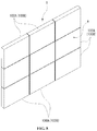
- FIG. 8 is a perspective view of a display system including the display device.
- FIG. 9 is a view illustrating the provisional junction of the electronic component to the vertical end surface of the display device by the provisional junction sub stance.
- FIG. 10 is a schematic cross-sectional view of a portion of a display device according to a second embodiment of the present disclosure.
- FIG. 11 is a schematic plane view of a portion of the display device of FIG. 10 .
- FIG. 12 is a schematic cross-sectional view of a display panel and an electronic component provisionally junctioned by a provisional junction substance.
- FIG. 1 is a schematic cross-sectional view of a portion of a display device according to a first embodiment of the present disclosure.
- FIG. 2 is a schematic plane view of a portion of the display device.
- FIG. 3 is a view showing an electronic component for the display device.
- FIG. 4 is a side view of the display device including a junction pad at a vertical side.
- FIG. 5 is a view illustrating a step of coating an auto-agglutination solder.
- FIG. 6 is a view illustrating a step of starting agglutination of the auto-agglutination solder particles.
- FIG. 7 is a view illustrating the junction of the electronic component to the vertical end surface of the display device by auto-agglutination of the auto-agglutination solder particles.
- FIG. 8 is a perspective view of a display system including the display device.
- FIG. 9 is a view illustrating the provisional junction of the electronic component to the vertical end surface of the display device by the
- a display device 100 A includes a display panel (e.g., a liquid crystal panel) 110 , a light source (not shown) that emits light toward the display panel 110 , and a light guiding part (not shown) that guides the light from the light source toward a rear side of the display panel 110 .
- the display panel 110 may be referred to as a substrate stack or a substrate device.
- the display panel 110 as the liquid crystal panel includes a first substrate (a substrate) 111 , a second substrate (a substrate) 112 facing the first substrate 111 and a liquid crystal layer (not shown) between the first and second substrates 111 and 112 .
- Each of the first and second substrates 111 and 112 may be one of a glass substrate, a resin substrate and a print substrate.
- a line part (a line) 113 which includes at least one signal line including a data line and a gate line, a thin film transistor, and so on, are formed.
- the liquid crystal layer is driven by the line part 113 such that the display panel 110 displays an image.
- the line part 113 may have a single-layered structure formed of a low resistance conductive material, e.g., aluminum (Al) or copper (Cu).
- the line part 113 may have a multi-layered structure including a first layer formed of a lower resistance conductive material, e.g., Al or Cu and a second layer formed of a conductive material, e.g., chrome (Cr), molybdenum (Mo) or titanium (Ti).
- a lower resistance conductive material e.g., Al or Cu
- a second layer formed of a conductive material e.g., chrome (Cr), molybdenum (Mo) or titanium (Ti).
- each line part 113 is a drawout part of the line part 113 .
- the end 113 e has a single-layered structure formed of a conductive material that is capable of forming an electrical junction with the solder.
- the conductive material for the end 113 e of the line part 113 may be one of tin (Sn), lead (Pb), zinc (Zn), silver (Ag) and copper (Cu).
- the end 113 e of the line part 113 may have a multi-layered structure including a first layer of the above conductive material and a second layer formed of Cr, Mo or Ti.
- the end surface 111 s of the first substrate 111 and the end surface 112 s of the second substrate 112 are disposed on the same plane.
- a vertical end surface 110 s which is perpendicular to a display surface 110 f , is formed (or defined) by the end surface 111 s of the first substrate 111 and the end surface 112 s of the second substrate 112 .
- the electronic component 130 is installed in the vertical end surface 110 s of the display panel 110 .
- the electronic component 130 may include a line substrate (a film substrate) 131 as a film type and a chip component 132 , e.g., a large scale integration (LSI), installed on a surface 131 f of the line substrate 131 .
- the electronic component 130 may be a chip on film (COF).
- COF chip on film
- On the surface 131 f of the line substrate 131 a plurality of connection electrodes (an electronic component side line connection part) 133 , which are respectively junctioned with the line parts 113 of the display panel 110 , are formed.
- the connection electrode 133 may be formed of a conductive material, e.g., Sn, Pb, Zn, Ag or Cu, that is capable of junctioning with the solder.
- connection pad 200 is junctioned to the end 113 e of each line part 113 between the first and second substrates 111 and 112 .
- the connection pad 200 which has a band shape and covers a portion of the first substrate 111 and a portion of the second substrate 112 , is formed along the vertical end surface 110 s of the display panel 110 .
- the connection pad 200 may be formed of a conductive material, e.g., Sn, Pb, Zn, Ag or Cu, that is capable of junctioning with the solder.
- connection pad 200 may be formed from a paste or a nano-ink of Ag or Cu by a screen printing process, a mesh-mask printing process or an ink-jet process.
- the connection pad 200 may have a width of about 10 to 100 ⁇ m, a length of about 0.1 to 1 mm and a thickness of about 10 to 1000 nm.
- the electronic component 130 is solder-junctioned to the connection pad 200 at the vertical end surface 110 s of the display panel 110 by an auto-agglutination solder 140 .
- the auto-agglutination solder 140 is a paste material.
- a solder particle 140 b formed of a solder-alloy material, e.g., Cu or Sn, is uniformly dispersed in a thermosetting resin 140 a .
- the thermosetting resin 140 a is formed of a material having a melting point lower than the solder particle 140 b .
- thermosetting resin 140 a for example, an epoxy resin, a urethane resin, an acrylic resin, a silicone resin, a phenol resin, a melamine resin, an alkyd resin, an urea resin, an unsaturated polyester resin, or the like, which has a melting point of 90° C. to 150° C., may be used.
- the material for forming the thermosetting resin 140 a exhibits fluidity at a temperature of the melting point or more.
- ‘Reflow Self Assembly Anisotropic Conductive Paste Epowell AP series’ SEKISUI CHEMICAL CO., LTD.
- ‘Low-Temperature-Curable conductive’ (Hitachi Chemical Co., Ltd.) may be used as the auto-agglutination solder 140 .
- a resin junction part (a low melting junction part) 160 is formed of a resin material having a melting point lower than the solder-alloy material for the solder particle 140 b contained in the auto-agglutination solder 140 .
- the resin junction part 160 may be formed of, for example, an epoxy resin, a urethane resin, an acrylic resin, a silicone resin, a phenol resin, a melamine resin, an alkyd resin, an urea resin, an unsaturated polyester resin, or the like, which has a melting point of 90° C. to 150° C. Moreover, the resin material for the resin junction part 160 is thermally cured when it is heated again above the melting point in order to create a soldering-junction using the auto-agglutination solder 140 after provisionally junctioning the electronic component 130 to the vertical end surface 110 s of the display panel 110 . This maintains the junction condition between the electronic component 130 and the vertical end surface 110 s of the display panel 110 .
- the junction of the electronic component 130 to the connection pad 200 at the vertical end surface 110 s of the display panel 110 is made using the auto-agglutination solder 140 .
- the auto-agglutination solder 140 is coated on the vertical end surface 110 s of the display panel 110 .
- the auto-agglutination solder 140 may be coated by a screen printing process, a mesh-mask printing process, or an ink-jet process.
- a provisional junction substance 161 is coated on each of upper and lower sides of a coating area of the auto-agglutination solder 140 .
- the provisional junction substance 161 has a thickness larger than a coating thickness of the auto-agglutination solder 140 in a direction facing the vertical end surface 110 s of the display panel 110 and the electronic component 130 . In this manner, the provisional junction substance 161 provided at the vertical end surface 110 s of the display panel 110 surely contacts the electronic component 130 during the provisional junctioning to be described later.
- the provisional junction substance 161 spreads upward and downward as compared with a coating area when the auto-agglutination solder 140 is thermally bonded, the provisional junction substance 161 , beneficially, is provided on a certain position that provisional junction substance 161 does not interfere with the auto-agglutination solder 140 considering the spread.
- the provisional junction substance 161 may be provided on only one of the upper and lower sides of the coating area of the auto-agglutination solder 140 .
- the provisional junction substance 161 may be applied to entirely surround the coating area of the auto-agglutination solder 140 .
- the provisional junction substance 161 may have a linear shape continuously formed in a direction along the display surface 110 f of the display panel 110 or may have a dot shape intermittently formed in the direction along the display surface 110 f of the display panel 110 .
- the provisional junction substance 161 finally forms the resin junction part 160 . Therefore, the provisional junction substance 161 is the same material as the resin junction part 160 .
- the provisional junction substance 161 may be provided ahead at the time of manufacturing the display panel 110 before application of the auto-agglutination solder 140 or may be provided before or after application of the auto-agglutination solder 140 for electrically joining the electronic component 130 to the display panel 110 .
- the provisional junction substance 161 already formed in a predetermined shape may be attached to the vertical end surface 110 s of the display panel 110 .
- connection pad 200 at the vertical end surface 110 s of the display panel 110 and the connection electrode 133 on the line substrate 131 of the electronic component 130 are aligned with a predetermined precision after application of the auto-agglutination solder 140 and the provisional junction part 160 .
- the provisional junction substance 161 is heated to a temperature lower than the melting point of the solder particle 140 b and the melting point of the provisional junction substance 161 by using the thermo-compressing device used in the junction process using the anisotropic conductive film (ACF). Then, the auto-agglutination solder 140 is not melted and the provisional junction substance 161 is softened.
- ACF anisotropic conductive film
- provisional junction substance 161 Thereafter, heating the provisional junction substance 161 is stopped. If the temperature of the provisional junction substance 161 decreases, the provisional junction substance 161 is cured, and the electronic component 130 is provisionally junctioned to the vertical end surface 110 s of the display panel 110 in a state in which the connection pad 200 provided on the vertical end surface 110 s of the display panel 110 and the connection electrode 133 formed on the line substrate 131 of the electronic component 130 are aligned.
- the vertical end surface 110 s of the display panel 110 and the electronic component 130 are pressed towards a direction approaching each other and heated using the thermo-compressing device used in the junction process using the anisotropic conductive film (ACF).
- a predetermined pressure and a predetermined temperature are applied to the auto-agglutination solder 140 during a predetermined time (period).
- the predetermined pressure may be applied to the auto-agglutination solder 140 under the temperature of 150° C. for 15 minutes.
- thermosetting resin 140 a and the solder particle 140 b are melted by the applied heat, and the solder particles 140 b in the thermosetting resin 140 a which have fluidity are aggregated to each other and become closer to the connection pad 200 and the connection electrode 133 .
- the solder particle 140 b is auto-agglutinated and metallically bonded at a space between the connection pad 200 and the connection electrode 133 , which are formed of a metallic material.
- connection pad 200 of the display panel 110 and the connection electrode 133 of the electronic component 130 are soldered by a solder metal (a solder junction part) “H” formed of a plurality of auto-agglutinated solder particles 140 b .
- the melted thermosetting resin 140 a is aggregated in a space between adjacent connection pads 200 and/or between adjacent connection electrodes 133 , such that the line substrate 131 of the electronic component 130 and the vertical end surface 110 s of the display panel 110 are attached to each other by an insulating resin (a resin adhesion part) “P” formed of the thermosetting resin 140 a.
- the auto-agglutination solder 140 is cooled after the thermo-compressing process such that the junction of the electronic component 130 to the vertical end surface 110 s of the display panel 110 is completed.
- the provisional junction substance 161 is melted by being heated above the melting point and then is cured by cooling. At this time, the provisional junction substance 161 heated above the melting point is thermally hardened, thereby maintaining the junction condition between the electronic component 130 and the vertical end surface 110 s of the display panel 110 .
- connection pad 200 at the vertical end surface 110 s of the display panel 110 and the connection electrode 133 on the line substrate 131 of the electronic component 130 are metallically bonded by the solder metal H of the auto-agglutination solder 140 such that the connection pad 200 and the connection electrode 133 are electrically connected.
- the vertical end surface 110 s of the display panel 110 and the line substrate 131 of the electronic component 130 are mechanically attached (or bonded) by the metal bond by the solder metal H and the adhesion by the insulating resin P.
- the mechanical junction between the vertical end surface 110 s of the display panel 110 and the line substrate 131 of the electronic component 130 by the solder metal H and the insulating resin P may have a tensile strength being equal to or greater than about 500 g/cm.
- the line substrate 131 of the electronic component 130 and the vertical end surface 110 s of the display panel 110 are also mechanically junctioned by the resin junction part 160 formed of the cured provisional junction substance 161 .
- solder metal H between the connection pad 200 and the connection electrode 133 may have a thickness being equal to or less than about 20 ⁇ m.
- a pitch of the connection pad 200 i.e., a distance between adjacent connection pads
- a pitch of the connection electrode 133 i.e., a distance between adjacent connection electrodes
- each may be about 10 to 100 ⁇ m.
- a bezel 150 which forms an outer case of the display device 100 A, is installed at a periphery of the display panel 110 where the electronic component 130 is installed.
- the bezel 150 may include a side plate part 150 a at an outer side of the vertical end surface 110 s of the display panel 110 and a front plate part 150 b extending from the side plate part 150 a toward a center of the display panel 110 and covering a front edge of the display surface 110 f of the display panel 110 .
- the electronic component 130 is accommodated in a space between the side plate part 150 a of the bezel 150 and the vertical end surface 110 s of the display panel 110 .
- the vertical end surface 110 s of the display panel 110 and the line substrate 131 of the electronic component 130 such that a width “w” of the bezel can be reduced. Namely, a narrow bezel display device 100 A is provided.
- a plurality of display devices 100 A of the narrow bezel are arranged to form a display system 1 .
- the plurality of display devices 100 A are adjacently arranged along a vertical direction and a horizontal direction.
- an image is displayed at a display region “A” formed by the plurality of display devices 100 A.
- the display system 1 includes the narrow bezel display devices 100 A, a gap between adjacent display devices 100 A is reduced such that a high quality image is provided at the display region “A.”
- An installation method of the electronic component 130 of the present disclosure includes disposing the provisional junction substance 161 formed of a material having the melting point lower than the solder particle 140 b of the auto-agglutination solder 140 between the vertical end surface 110 s of the display panel 110 and the electronic component 130 , while disposing the connection electrode 133 of the electronic component 130 to face the vertical end surface 110 s of the display panel 110 including the connection pad 200 at the end 113 e of the line part 113 between the first substrate 111 and the second substrate 112 .
- the installation method further includes interposing (or coating) the auto-agglutination solder 140 , which includes the thermosetting resin 140 a and the solder particle 140 b , between the connection electrode 133 and the connection pad 200 .
- the installation method also includes provisionally junctioning the electronic component 130 and the vertical end surface 110 s of the display panel 110 by softening the provisional junction substance 161 at the temperature lower than the melting point of the solder particle 140 b and lower than the melting point of the provisional junction substance 161 . Additionally, the installation method includes pressurizing and junctioning the connection electrode 133 to the connection pad 200 in a direction approaching each other by heating-up the auto-agglutination solder 140 and the provisional junction substance 161 .
- connection electrode 133 of the electronic component 130 and the connection pad 200 can be aligned with a high precision.
- the junction process for the electronic component 130 and the display panel 110 can be efficiently carried out by soldering with the auto-agglutination solder 140 , after provisionally junctioning the electronic component 130 and the display panel 110 with the provisional junction substance 161 .
- connection electrode 133 of the electronic component 130 and the connection pad 200 may be aligned again by heating again and softening the provisional junction substance 161 if it is before junctioning with the auto-agglutination solder 140 .
- solder metal H which is created by the aggregation of the solder particles 140 b , is formed between the connection electrode 133 and the connection pad 200 .
- the amount of the conductive particles between the connection electrode 133 and the connection pad 200 is increased such that the increase of the contact (or connection) resistance between the connection electrode 133 and the connection pad 200 is prevented.
- the vertical end surface 110 s of the display panel 110 and the electronic component 130 are mechanically attached (or bonded) by the metal bond of the solder metal H of the solder particle 140 b and by the adhesion of the insulating resin P of the thermosetting resin 140 b .
- the electronic component 130 and the vertical end surface 110 s of the display panel 110 are also junctioned around the auto-agglutination solder 140 by the resin junction part 160 (the provisional junction substance 161 ). Therefore, the electronic component 130 is securely junctioned.
- junction part “J” that electrically joins the connection pad 200 at the vertical end surface 110 s of the display panel 110 (which includes the first substrate 111 , the second substrate 112 and the connection pad 200 at the end 113 e of the line part 113 between the first and second substrates 111 and 112 ) with the electronic component 130 (which includes the connection electrode 133 facing the vertical end surface 110 s of the display panel 110 ).
- the junction part “J” includes the solder metal “H” between the connection pad 200 and the connection electrode 133 , the insulating resin “P” attaching (adhering) the vertical end surface 110 s and the electronic component 130 in a region outside the solder metal “H,” and the resin junction part 160 formed of a material having a lower melting point than the solder metal “H” between the vertical end surface 110 s of the display panel 110 and the electronic component 130 .
- the electronic component 130 is securely combined (junctioned or connected) to the vertical end surface 110 s of the display panel 110 , and the electric connection property is increased such that the increase of the connection resistance (contact resistance) is prevented.
- FIG. 10 is a schematic cross-sectional view of a portion of a display device according to a second embodiment of the present disclosure.
- FIG. 11 is a schematic plane view of a portion of the display device.
- FIG. 12 is a schematic cross-sectional view of a display panel and an electronic component provisionally junctioned by a provisional junction substance.
- the same reference numbers are used to the same elements as the first embodiment, and the explanation for those may be omitted.
- a display device 100 B includes a display panel (e.g., a liquid crystal panel) 110 , a light source (not shown) that emits light toward the display panel 110 , and a light guiding part (not shown) that guides the light from the light source toward a rear side of the display panel 110 .
- the display panel 110 may be referred to as a substrate stack or a substrate device.
- the display panel 110 as the liquid crystal panel includes a first substrate (a substrate) 111 , a second substrate (a substrate) 112 facing the first substrate 111 and a liquid crystal layer (not shown) between the first and second substrates 111 and 112 .
- Each of the first and second substrates 111 and 112 may be one of a glass substrate, a resin substrate and a print substrate.
- a line part (a line) 113 which includes a signal line including a data line and a gate line, a thin film transistor, and so on, are formed.
- the liquid crystal layer is driven by the line part 113 such that the display device 100 A provides an image.
- the line part 113 may have a single-layered structure formed of a low resistance conductive material, e.g., aluminum (Al) or copper (Cu).
- the line part 113 may have a multi-layered structure including a first layer formed of a lower resistance conductive material, e.g., Al or Cu and a second layer formed of a conductive material, e.g., chrome (Cr), molybdenum (Mo) or titanium (Ti).
- a lower resistance conductive material e.g., Al or Cu
- a second layer formed of a conductive material e.g., chrome (Cr), molybdenum (Mo) or titanium (Ti).
- An end part 113 s of each line part 113 is a drawout part of the line part 113 and has a single-layered structure formed of a conductive material that is capable of forming the electrical junction with the solder.
- the conductive material for the end part 113 s of the line part 113 may be one of tin (Sn), lead (Pb), zinc (Zn), silver (Ag) and copper (Cu).
- the end part 113 s of the line part 113 may have a multi-layered structure including a first layer of the above conductive material and a second layer formed of Cr, Mo or Ti.
- the end surface 111 s of the first substrate 111 and the end surface 112 s of the second substrate 112 are disposed on the same plane.
- a vertical end surface 110 s which is perpendicular to a display surface 110 f , is formed (or defined) by the end surface 111 s of the first substrate 111 and the end surface 112 s of the second substrate 112 .
- the end part 113 s of the line part 113 (a substrate side line connection part) is disposed on the same plane with the end surface 111 s of the first substrate 111 and the end surface 112 s of the second substrate 112 such that the end part 113 s of the line part 113 is exposed.
- the electronic component 130 may include a line substrate (a film substrate) 131 as a film type and a chip component 132 , e.g., a large scale integration (LSI), installed (or arranged) on a surface 131 f of the line substrate 131 .
- the electronic component 130 may be a chip on film (COF).
- COF chip on film
- connection electrode 133 may be formed of a conductive material, e.g., Sn, Pb, Zn, Ag or Cu, that is capable of junctioning with the solder.
- a vertical length (length) of the connection electrode 133 along a direction from the first substrate 111 to the second substrate 112 (or the second substrate 112 to the first substrate 111 ) is larger than that of the substrate side line connection part 113 s (i.e., the end of the line part 113 ).
- the electronic component 130 is solder-junctioned to the end part (i.e., the substrate side line connection part) 113 s of the line part 113 , which is exposed at the vertical end surface 110 s of the display panel 110 , by an auto-agglutination solder 140 .
- the auto-agglutination solder 140 is a paste material.
- a solder particle 140 b formed of a solder-alloy material, e.g., Cu or Sn is uniformly dispersed in a thermosetting resin 140 a .
- the thermosetting resin 140 a is formed of a material having a melting point lower than the solder particle 140 b .
- thermosetting resin 140 a for example, an epoxy resin, a urethane resin, an acrylic resin, a silicone resin, a phenol resin, a melamine resin, an alkyd resin, an urea resin, an unsaturated polyester resin, or the like, which has a melting point of 90° C. to 150° C., may be used.
- the material for forming the thermosetting resin 140 a exhibits fluidity at a temperature of the melting point or more.
- ‘Reflow Self Assembly Anisotropic Conductive Paste Epowell AP series’ SEKISUI CHEMICAL CO., LTD.
- ‘Low-Temperature-Curable conductive’ (Hitachi Chemical Co., Ltd.) may be used as the auto-agglutination solder 140 .
- a resin junction part 160 is formed of a resin material having a melting point lower than the auto-agglutination solder 140 .
- the resin junction part 160 may be formed of, for example, an epoxy resin, a urethane resin, an acrylic resin, a silicone resin, a phenol resin, a melamine resin, an alkyd resin, an urea resin, an unsaturated polyester resin, or the like, which has a melting point of 90° C. to 150° C.
- the resin material for the resin junction part 160 is thermally cured when it is heated again above the melting point in order to create a solder-junction using the auto-agglutination solder 140 after provisionally junctioning the electronic component 130 to the vertical end surface 110 s of the display panel 110 . This maintains the junction condition between the electronic component 130 and the vertical end surface 110 s of the display panel 110 .
- the junction of the electronic component 130 to the end part 113 s at the vertical end surface 110 s of the display panel 110 is made using the auto-agglutination solder 140 .
- the auto-agglutination solder 140 is coated on the vertical end surface 110 s of the display panel 110 .
- the auto-agglutination solder 140 of the paste phase may be coated by a screen printing process, a mesh-mask printing process, or an ink-jet process.
- a provisional junction substance 161 is coated on each of upper and lower sides of a coating area of the auto-agglutination solder 140 .
- the provisional junction substance 161 has a thickness larger than a coating thickness of the auto-agglutination solder 140 in a direction facing the vertical end surface 110 s of the display panel 110 and the electronic component 130 . In this manner, the provisional junction substance 161 provided at the vertical end surface 110 s of the display panel 110 surely contacts the electronic component 130 during the provisional junctioning to be described later.
- the provisional junction substance 161 spreads upward and downward as compared with a coating area when the auto-agglutination solder 140 is thermally bonded, the provisional junction substance 161 , beneficially, is provided on a certain position that provisional junction substance 161 does not interfere with the auto-agglutination solder 140 considering the spread.
- the provisional junction substance 161 may be provided on only one of the upper and lower sides of the coating area of the auto-agglutination solder 140 . That is, the provisional junction substance 161 may be provided on only one of the end surface 111 s of the first substrate 111 and the end surface 112 s of the second substrate 112 . In addition, the provisional junction substance 161 may be applied to entirely surround the coating area of the auto-agglutination solder 140 .
- the provisional junction substance 161 may have a linear shape continuously formed in a direction along the display surface 110 f of the display panel 110 or may have a dot shape intermittently formed in the direction along the display surface 110 f of the display panel 110 .
- the provisional junction substance 161 finally forms the resin junction part 160 . Therefore, the provisional junction substance 161 is the same material as the resin junction part 160 .
- the provisional junction substance 161 may be provided ahead at the time of manufacturing the display panel 110 before application of the auto-agglutination solder 140 or may be provided before or after application of the auto-agglutination solder 140 for electrically joining the electronic component 130 to the display panel 110 .
- the provisional junction substance 161 already formed in a predetermined shape may be attached to the vertical end surface 110 s of the display panel 110 .
- the end part 113 s of the line part 113 exposed at the vertical end surface 110 s of the display panel 110 and the connection electrode 133 on the line substrate 131 of the electronic component 130 are aligned with a predetermined precision after application of the auto-agglutination solder 140 and the provisional junction part 160 .
- the provisional junction substance 161 is heated to a temperature lower than the melting point of the solder particle 140 b and the melting point of the provisional junction substance 161 by using the thermo-compressing device used in the junction process using anisotropic conductive film (ACF). Then, the auto-agglutination solder 140 is not melted and the provisional junction substance 161 is softened.
- ACF anisotropic conductive film
- provisional junction substance 161 Thereafter, heating the provisional junction substance 161 is stopped. If the temperature of the provisional junction substance 161 decreases, the provisional junction substance 161 is cured, and the electronic component 130 is provisionally junctioned to the vertical end surface 110 s of the display panel 110 in a state in which the end part 113 s of the line part 113 exposed at the vertical end surface 110 s of the display panel 110 and the connection electrode 133 formed on the line substrate 131 of the electronic component 130 are aligned.
- the vertical end surface 110 s of the display panel 110 and the electronic component 130 are pressed in a direction approaching each other and heated using the thermo-compressing device used in the junction process using the anisotropic conductive film (ACF).
- a predetermined pressure and a predetermined temperature are applied to the auto-agglutination solder 140 during a predetermined period of time).
- the predetermined pressure may be applied to the end part 113 s of the line part 113 exposed at the vertical end surface 110 s of the display panel 110 and the connection electrode 133 on the line substrate 131 of the electronic component 130 under the temperature of 150° C. for 15 minutes.
- thermosetting resin 140 a and the solder particle 140 b are melted by the applied heat, and the solder particles 140 b in the thermosetting resin 140 a which have fluidity are aggregated to each other and metallically bonded at a space between the end part 113 s of the line part 113 and the connection electrode 133 , which are formed of a metallic material.
- the end part 113 s of the line part 113 of the display panel 110 and the connection electrode 133 of the electronic component 130 are soldered by a solder metal (a solder junction part) “H” formed of a plurality of auto-agglutinated solder particles 140 b .
- thermosetting resin 140 a is aggregated such that an insulating resin (a resin adhesion part) “P” is formed of the thermosetting resin 140 a in an area other than a portion where the solder metal H is formed.
- the auto-agglutination solder 140 is cooled after the thermo-compressing process such that the junction of the electronic component 130 to the vertical end surface 110 s of the display panel 110 is completed.
- the provisional junction substance 161 is melted by being heated above the melting point and then is cured by cooling. At this time, the provisional junction substance 161 heated above the melting point is thermally hardened, thereby maintaining the junction condition between the electronic component 130 and the vertical end surface 110 s of the display panel 110 .
- the end part 113 s of the line part 113 which is exposed at the vertical end surface 110 s of the display panel 110 and the connection electrode 133 on the line substrate 131 of the electronic component 130 are selectively metallically bonded by the solder metal H of the auto-agglutination solder 140 to be electrically connected.
- the vertical end surface 110 s of the display panel 110 and the line substrate 131 of the electronic component 130 are mechanically attached (or bonded) by the metal bond using the solder metal H and the adhesion using the insulating resin P.
- the mechanical junction between the vertical end surface 110 s of the display panel 110 and the line substrate 131 of the electronic component by the solder metal H and the insulating resin P may have a tensile strength being equal to or greater than about 500 g/cm.
- the line substrate 131 of the electronic component 130 and the vertical end surface 110 s of the display panel 110 are also mechanically junctioned by the resin junction part 160 formed of the cured provisional junction substance 161 .
- solder metal H between the end part 113 s and the connection electrode 133 may have a thickness being equal to or less than about 20 ⁇ m.
- a pitch of the end part 113 s and a pitch of the connection electrode 133 each may be about 10 to 100 ⁇ m.
- a bezel 150 which forms an outer case of the display device 100 B, is installed at a periphery of the display panel 110 where the electronic component 130 is installed.
- the bezel 150 may include a side plate part 150 a at an outer side of the vertical end surface 110 s of the display panel 110 and a front plate part 150 b extending from the side plate part 150 a toward a center of the display panel 110 and covering a front edge of the display surface 110 f of the display panel 110 .
- the electronic component 130 is accommodated in a space between the side plate part 150 a of the bezel 150 and the vertical end surface 110 s of the display panel 110 .
- the vertical end surface 110 s of the display panel 110 and the line substrate 131 of the electronic component 130 such that a width “w” of the bezel can be reduced. Namely, a narrow bezel display device 100 B is provided.
- a plurality of display devices 100 B of the narrow bezel are arranged to form a display system 1 as shown in FIG. 8 .
- the plurality of display devices 100 B are adjacently arranged along a vertical direction and a horizontal direction.
- an image is displayed at a display region “A” formed by the plurality of display devices 100 B.
- the display system 1 includes the narrow bezel display devices 100 B, a gap between adjacent display devices 100 B is reduced such that a high quality image is provided at the display region “A.”
- An installation method of the electronic component 130 of the present disclosure includes disposing the provisional junction substance 161 formed of a material having the melting point lower than the solder particle 140 b of the auto-agglutination solder 140 between the vertical end surface 110 s of the display panel 110 and the electronic component 130 , while disposing the connection electrode 133 of the electronic component 130 to face the vertical end surface 110 s of the display panel 110 including the line part 113 installed between the first substrate 111 and the second substrate 112 .
- the installation method further includes interposing (or coating) the auto-agglutination solder 140 , which includes the thermosetting resin 140 a and the solder particle 140 b , between the connection electrode 133 and the end part 113 s of the line part.
- the installation method also includes provisionally junctioning the electronic component 130 and the vertical end surface 110 s of the display panel 110 by softening the provisional junction substance 161 at the temperature lower than the melting point of the solder particle 140 b and lower than the melting point of the provisional junction substance 161 . Additionally, the installation method includes pressurizing and junctioning the connection electrode 133 to the end part 113 s in a direction approaching each other by heating-up the auto-agglutination solder 140 and the provisional junction substance 161 .
- connection electrode 133 of the electronic component 130 and the end part 113 s of the line part 113 can be aligned with a high precision.
- the junction process for the electronic component 130 and the display panel 110 can be efficiently carried out by soldering with the auto-agglutination solder 140 , after provisionally junctioning the electronic component 130 and the display panel 110 with the provisional junction substance 161 .
- connection electrode 133 of the electronic component 130 and the end part 113 s of the line part 113 may be aligned again by heating again and softening the provisional junction substance 161 if it is before junctioning with the auto-agglutination solder 140 .
- the solder metal H which is created by the aggregation of the solder particles 140 b , is formed between the connection electrode 133 and the end part 113 s of the line part 113 .
- the amount of the conductive particles between the connection electrode 133 and the end part 113 s of the line part 113 is increased such that the increase of the contact (or connection) resistance between the connection electrode 133 and the end part 113 s of the line part 113 is prevented.
- the vertical end surface 110 s of the display panel 110 and the electronic component 130 are mechanically attached (or bonded) by the metal bond of the solder metal H of the solder particle 140 b and by the adhesion of the insulating resin P of the thermosetting resin 140 b .
- the electronic component 130 and the vertical end surface 110 s of the display panel 110 are also junctioned around the auto-agglutination solder 140 by the resin junction part 160 (the provisional junction substance 161 ). Therefore, the electronic component 130 is securely junctioned.
- connection part 200 is not required as compared with the first embodiment. Accordingly, the process of forming the connection pad 200 is omitted such that the production efficiency is increased and the production cost is decreased.
- junction part “J” that electrically joins the end part 113 s of the line part 113 at the vertical end surface 110 s of the display panel 110 (which includes the first substrate 111 , the second substrate 112 and the line part 113 between the first and second substrates 111 and 112 ) with the electronic component 130 (which includes the connection electrode 133 facing the vertical end surface 110 s of the display panel 110 ).
- the junction part “J” includes the solder metal “H” between the end part 113 s of the line part 113 and the connection electrode 133 , the insulating resin “P” attaching (adhering) the vertical end surface 110 s and the electronic component 130 in a region outside the solder metal “H,” and the resin junction part 160 formed of a material having a lower melting point than the solder metal “H” between the vertical end surface 110 s of the display panel 110 and the electronic component 130 .
- the electronic component 130 is securely combined (junctioned or connected) to the vertical end surface 110 s of the display panel 110 , and the electric connection property is increased such that the increase of the connection resistance (contact resistance) is prevented.
- the provisional junction substance 161 may be provided on the vertical end surface 110 s of the liquid crystal panel 110 .
- the provisional junction substance 161 may be provided on the electronic component 130 or may be provided on both the vertical end surface 110 s of the display panel 110 and the electronic component 130 .
- the installing method of the electronic component 130 and the bonding structure of the electronic component 130 shown in each of the above embodiments can be applied to various electronic devices in addition to the display devices 100 A and 100 B.
- the display devices 100 A and 100 B are not limited to the liquid crystal display device, and the present disclosure can be similarly applied to an organic light emitting diode display device, a plasma display panel display device, and the like.
Abstract
A display device includes a substrate stack including two substrates, a line between the two substrates, and a substrate side line connection part at an end of the line. The display device also includes an electronic component having an electronic component side line connection part. The electronic component side line connection part faces a vertical end surface of the substrate stack. The display device further includes a junction part that electrically joins the vertical end surface and the electronic component. The junction part includes a solder junction part between the substrate side line connection part and the electronic component side line connection part, a resin adhesion part at a region outside the solder junction part that adheres the vertical end surface and the electronic component, and a low-melting junction part between the vertical end surface and the electronic component and formed of a material having a melting point lower than the solder particle.
Description
The present application is a divisional application of U.S. patent application Ser. No. 15/717,769 filed on Sep. 27, 2017, which claims priority from and the benefit under 35 U.S.C. § 119(a) of Japanese Patent Application No. 2016-189588 filed on Sep. 28, 2016, which is hereby incorporated by reference in its entirety.
The present disclosure relates to a display device, a display system, and a method of installing or mounting an electronic component.
Generally, the electronic component for the electronic device is installed on a surface of a substrate by joining a pad part of the electronic component to a line pattern on the substrate.
For example, Japanese Patent Publication No. 2012-226058 discloses a connection method of the line pattern of the substrate and a line connection part of the electronic component by using an anisotropic conductive film (ACF). The anisotropic conductive film includes conductive particles dispersed in a thermosetting resin (thermohardening resin or thermally-curable resin). The line pattern of the substrate and the line connection part of the electronic component are electrically connected to each other by the anisotropic conductive film.
When the anisotropic conductive film is used as disclosed in Japanese Patent Publication No. 2012-226058, the conductive particles physically contact with the line pattern of the substrate and the line connection part of the electronic component, and thus the line pattern of the substrate and the line connection part of the electronic component are electrically connected to each other. However, since the conductive particles are dispersed in the thermosetting resin, the connection resistance tends to increase.
In addition, between the substrate and the electronic component, there exists an insulated part other than the junction part between the line pattern of the substrate and the line connection part of the electronic component. Some of the conductive particles dispersed in the thermosetting resin are interposed between the substrate and the electronic component corresponding to the insulated part. This decreases the insulating properties in the insulated part.
Furthermore, recently in display devices, the display image has become finer, and the pitch (interval) of the line pattern of the substrate has narrowed to, for example, 100 μm or less. When the line pattern having the narrow pitch is used, problems such as an increase in the connection resistance and a decrease in the insulating properties due to use of the anisotropic conductive film become more significant.
Accordingly, the electrical connection must be increased, thereby suppressing the connection resistance, while firmly bonding the electronic component to the substrate.
Additionally, in embodiments where the line connection part of the electronic component is connected to the substrate having the narrow pitch line pattern as described above, high positioning accuracy of the line pattern of the substrate and the line connection part of the electronic component is required.
However, when the line pattern of the substrate and the line connection part of the electronic component are bonded to each other, the line pattern of the substrate and the line connection part of the electronic component may be deviated.
As such, there is a continuing need in the art for a method of installing or mounting electronic components that do not have these limitations.
Accordingly, the present disclosure is directed to a display device, a display system, and a method of installing or mounting an electronic component. The disclosed method substantially obviates one or more technological problems due to limitations of the related art.
In at least one embodiment, the present disclosure provides a display device, a display system, and a method of installing or mounting an electronic component that can align an electronic component with high accuracy with respect to a line pattern of a substrate board, firmly bond the electronic component to the end surface of the substrate, and increase the electrical connection, thereby suppressing the connection resistance.
Additional features and embodiments of the present disclosure will be set forth in the description which follows, and will be apparent from the description. The technological improvements of the present disclosure will be realized and attained by the structure particularly pointed out in the written description and claims hereof as well as the appended drawings.
In accordance with the present disclosure, as embodied and broadly described herein, there is provided a method of installing an electronic component that includes disposing the electronic component having an electronic component side line connection part at a vertical end surface of a substrate stack including two substrates, a line between the two substrates, and a substrate side line connection part at an end of the line. The electronic component side line connection part faces the vertical end surface. The method further includes forming an auto-agglutination solder between the electronic component side line connection part and the substrate side line connection part. The auto-agglutination solder includes a thermosetting resin and a solder particle. Additionally, the method includes forming a provisional junction substance between the vertical end surface of the substrate stack and the electronic component, the provisional junction substance formed of a material having a melting point lower than the solder particle. The method also includes provisionally junctioning the electronic component and the vertical end surface of the substrate stack by softening the provisional junction substance at a temperature lower than a melting point of the solder particle and the melting point of the provisional junction substance. The method additionally includes pressurizing the electronic component side line connection part and the substrate side line connection part by heating-up the auto-agglutination solder and the provisional junction substance.
In another embodiment, the present disclosure is directed towards a display device includes a substrate stack including two substrates, a line between the two substrates, and a substrate side line connection part at an end of the line. The display device further includes an electronic component having an electronic component side line connection part. The electronic component side line connection part faces a vertical end surface of the substrate stack. Additionally, the display device includes a junction part that electrically joins the vertical end surface and the electronic component. The junction part includes a solder junction part between the substrate side line connection part and the electronic component side line connection part. The junction part also includes a resin adhesion part at a region outside the solder junction part that adheres the vertical end surface and the electronic component. The junction part further includes a low-melting junction part between the vertical end surface and the electronic component and formed of a material having a melting point lower than the solder particle.
In another embodiment, the present disclosure is directed towards a display system that includes a first display device, a second display device adjacent to the first display device along a first direction, and a third display device adjacent to the first display device along a second direction. At least one of the first, second, and third display devices includes: a substrate stack having two substrates, a line between the two substrates, and a substrate side line connection part at an end of the line; an electronic component having an electronic component side line connection part, the electronic component side line connection part facing a vertical end surface of the substrate stack; and a junction part that electrically joins the vertical end surface and the electronic component. The junction part includes a solder junction part between the substrate side line connection part and the electronic component side line connection part. The junction part also includes a resin adhesion part at a region outside the solder junction part that adheres the vertical end surface and the electronic component. The junction part further includes a low-melting junction part between the vertical end surface and the electronic component and formed of a material having a melting point lower than the solder particle.
The foregoing general description and the following detailed description are by example and explanatory and are intended to provide further explanation of the present disclosure as claimed.
The accompanying drawings, which are included to provide a further understanding of the present disclosure and which are incorporated in and constitute a part of this specification, illustrate embodiments of the present disclosure and together with the description serve to explain the principles of the present disclosure. In the drawings:
Reference will now be made in detail to embodiments of the disclosure, examples of which are illustrated in the accompanying drawings.
Referring to FIGS. 1 and 2 , a display device 100A includes a display panel (e.g., a liquid crystal panel) 110, a light source (not shown) that emits light toward the display panel 110, and a light guiding part (not shown) that guides the light from the light source toward a rear side of the display panel 110. The display panel 110 may be referred to as a substrate stack or a substrate device.
The display panel 110 as the liquid crystal panel includes a first substrate (a substrate) 111, a second substrate (a substrate) 112 facing the first substrate 111 and a liquid crystal layer (not shown) between the first and second substrates 111 and 112.
Each of the first and second substrates 111 and 112 may be one of a glass substrate, a resin substrate and a print substrate.
Although not shown in the figures, on at least one of the first and second substrates 111 and 112 (e.g., the first substrate 111), a line part (a line) 113, which includes at least one signal line including a data line and a gate line, a thin film transistor, and so on, are formed. The liquid crystal layer is driven by the line part 113 such that the display panel 110 displays an image. The line part 113 may have a single-layered structure formed of a low resistance conductive material, e.g., aluminum (Al) or copper (Cu). Alternatively, the line part 113 may have a multi-layered structure including a first layer formed of a lower resistance conductive material, e.g., Al or Cu and a second layer formed of a conductive material, e.g., chrome (Cr), molybdenum (Mo) or titanium (Ti).
An end 113 e of each line part 113 is a drawout part of the line part 113. The end 113 e has a single-layered structure formed of a conductive material that is capable of forming an electrical junction with the solder. The conductive material for the end 113 e of the line part 113 may be one of tin (Sn), lead (Pb), zinc (Zn), silver (Ag) and copper (Cu). Alternatively, the end 113 e of the line part 113 may have a multi-layered structure including a first layer of the above conductive material and a second layer formed of Cr, Mo or Ti.
In the display panel 110, the end surface 111 s of the first substrate 111 and the end surface 112 s of the second substrate 112 are disposed on the same plane. At the end of the display panel 110, a vertical end surface 110 s, which is perpendicular to a display surface 110 f, is formed (or defined) by the end surface 111 s of the first substrate 111 and the end surface 112 s of the second substrate 112.
In the vertical end surface 110 s of the display panel 110, the electronic component 130 is installed. As shown in FIGS. 1 and 3 , the electronic component 130 may include a line substrate (a film substrate) 131 as a film type and a chip component 132, e.g., a large scale integration (LSI), installed on a surface 131 f of the line substrate 131. For example, the electronic component 130 may be a chip on film (COF). On the surface 131 f of the line substrate 131, a plurality of connection electrodes (an electronic component side line connection part) 133, which are respectively junctioned with the line parts 113 of the display panel 110, are formed. The connection electrode 133 may be formed of a conductive material, e.g., Sn, Pb, Zn, Ag or Cu, that is capable of junctioning with the solder.
As shown in FIGS. 1 and 4 , to install the electronic component 130, a connection pad (a substrate side line connection part) 200 is junctioned to the end 113 e of each line part 113 between the first and second substrates 111 and 112. The connection pad 200, which has a band shape and covers a portion of the first substrate 111 and a portion of the second substrate 112, is formed along the vertical end surface 110 s of the display panel 110. The connection pad 200 may be formed of a conductive material, e.g., Sn, Pb, Zn, Ag or Cu, that is capable of junctioning with the solder.
In some embodiments, the connection pad 200 may be formed from a paste or a nano-ink of Ag or Cu by a screen printing process, a mesh-mask printing process or an ink-jet process. For example, the connection pad 200 may have a width of about 10 to 100 μm, a length of about 0.1 to 1 mm and a thickness of about 10 to 1000 nm.
As shown in FIGS. 1 and 2 , the electronic component 130 is solder-junctioned to the connection pad 200 at the vertical end surface 110 s of the display panel 110 by an auto-agglutination solder 140. As shown in FIG. 5 , the auto-agglutination solder 140 is a paste material. In the auto-agglutination solder 140, a solder particle 140 b formed of a solder-alloy material, e.g., Cu or Sn, is uniformly dispersed in a thermosetting resin 140 a. The thermosetting resin 140 a is formed of a material having a melting point lower than the solder particle 140 b. As the material for forming the thermosetting resin 140 a, for example, an epoxy resin, a urethane resin, an acrylic resin, a silicone resin, a phenol resin, a melamine resin, an alkyd resin, an urea resin, an unsaturated polyester resin, or the like, which has a melting point of 90° C. to 150° C., may be used. Here, the material for forming the thermosetting resin 140 a exhibits fluidity at a temperature of the melting point or more.
For example, ‘Reflow Self Assembly Anisotropic Conductive Paste Epowell AP series’ (SEKISUI CHEMICAL CO., LTD.) or ‘Low-Temperature-Curable conductive’ (Hitachi Chemical Co., Ltd.) may be used as the auto-agglutination solder 140.
In addition, around the auto-agglutination solder 140 junctioning the vertical end surface 110 s of the display panel 110 and the electronic component 130, more particularly, at each of an upper side and a lower side of the auto-agglutination solder 140, a resin junction part (a low melting junction part) 160 is formed of a resin material having a melting point lower than the solder-alloy material for the solder particle 140 b contained in the auto-agglutination solder 140. The resin junction part 160 may be formed of, for example, an epoxy resin, a urethane resin, an acrylic resin, a silicone resin, a phenol resin, a melamine resin, an alkyd resin, an urea resin, an unsaturated polyester resin, or the like, which has a melting point of 90° C. to 150° C. Moreover, the resin material for the resin junction part 160 is thermally cured when it is heated again above the melting point in order to create a soldering-junction using the auto-agglutination solder 140 after provisionally junctioning the electronic component 130 to the vertical end surface 110 s of the display panel 110. This maintains the junction condition between the electronic component 130 and the vertical end surface 110 s of the display panel 110.
The junction of the electronic component 130 to the connection pad 200 at the vertical end surface 110 s of the display panel 110 is made using the auto-agglutination solder 140. In some embodiments, the auto-agglutination solder 140 is coated on the vertical end surface 110 s of the display panel 110. For example, the auto-agglutination solder 140 may be coated by a screen printing process, a mesh-mask printing process, or an ink-jet process.
In addition, as shown in FIGS. 4 and 9 , at the vertical end surface 110 s of the display panel 110, a provisional junction substance 161 is coated on each of upper and lower sides of a coating area of the auto-agglutination solder 140. In some embodiments, the provisional junction substance 161 has a thickness larger than a coating thickness of the auto-agglutination solder 140 in a direction facing the vertical end surface 110 s of the display panel 110 and the electronic component 130. In this manner, the provisional junction substance 161 provided at the vertical end surface 110 s of the display panel 110 surely contacts the electronic component 130 during the provisional junctioning to be described later.
Moreover, since the provisional junction substance 161 spreads upward and downward as compared with a coating area when the auto-agglutination solder 140 is thermally bonded, the provisional junction substance 161, beneficially, is provided on a certain position that provisional junction substance 161 does not interfere with the auto-agglutination solder 140 considering the spread.
Alternatively, the provisional junction substance 161 may be provided on only one of the upper and lower sides of the coating area of the auto-agglutination solder 140. In addition, the provisional junction substance 161 may be applied to entirely surround the coating area of the auto-agglutination solder 140.
Furthermore, the provisional junction substance 161 may have a linear shape continuously formed in a direction along the display surface 110 f of the display panel 110 or may have a dot shape intermittently formed in the direction along the display surface 110 f of the display panel 110. The provisional junction substance 161 finally forms the resin junction part 160. Therefore, the provisional junction substance 161 is the same material as the resin junction part 160.
The provisional junction substance 161 may be provided ahead at the time of manufacturing the display panel 110 before application of the auto-agglutination solder 140 or may be provided before or after application of the auto-agglutination solder 140 for electrically joining the electronic component 130 to the display panel 110. Alternatively, the provisional junction substance 161 already formed in a predetermined shape may be attached to the vertical end surface 110 s of the display panel 110.
The connection pad 200 at the vertical end surface 110 s of the display panel 110 and the connection electrode 133 on the line substrate 131 of the electronic component 130 are aligned with a predetermined precision after application of the auto-agglutination solder 140 and the provisional junction part 160.
The provisional junction substance 161 is heated to a temperature lower than the melting point of the solder particle 140 b and the melting point of the provisional junction substance 161 by using the thermo-compressing device used in the junction process using the anisotropic conductive film (ACF). Then, the auto-agglutination solder 140 is not melted and the provisional junction substance 161 is softened.
Thereafter, heating the provisional junction substance 161 is stopped. If the temperature of the provisional junction substance 161 decreases, the provisional junction substance 161 is cured, and the electronic component 130 is provisionally junctioned to the vertical end surface 110 s of the display panel 110 in a state in which the connection pad 200 provided on the vertical end surface 110 s of the display panel 110 and the connection electrode 133 formed on the line substrate 131 of the electronic component 130 are aligned.
Next, the vertical end surface 110 s of the display panel 110 and the electronic component 130 are pressed towards a direction approaching each other and heated using the thermo-compressing device used in the junction process using the anisotropic conductive film (ACF). A predetermined pressure and a predetermined temperature are applied to the auto-agglutination solder 140 during a predetermined time (period). For example, the predetermined pressure may be applied to the auto-agglutination solder 140 under the temperature of 150° C. for 15 minutes.
As shown in FIG. 6 , the thermosetting resin 140 a and the solder particle 140 b are melted by the applied heat, and the solder particles 140 b in the thermosetting resin 140 a which have fluidity are aggregated to each other and become closer to the connection pad 200 and the connection electrode 133. As a result, as shown in FIG. 7 , the solder particle 140 b is auto-agglutinated and metallically bonded at a space between the connection pad 200 and the connection electrode 133, which are formed of a metallic material. Namely, the connection pad 200 of the display panel 110 and the connection electrode 133 of the electronic component 130 are soldered by a solder metal (a solder junction part) “H” formed of a plurality of auto-agglutinated solder particles 140 b. Additionally, the melted thermosetting resin 140 a is aggregated in a space between adjacent connection pads 200 and/or between adjacent connection electrodes 133, such that the line substrate 131 of the electronic component 130 and the vertical end surface 110 s of the display panel 110 are attached to each other by an insulating resin (a resin adhesion part) “P” formed of the thermosetting resin 140 a.
The auto-agglutination solder 140 is cooled after the thermo-compressing process such that the junction of the electronic component 130 to the vertical end surface 110 s of the display panel 110 is completed.
In addition, while the auto-agglutination solder 140 is heated and pressed in the thermo-compressing process, the provisional junction substance 161 is melted by being heated above the melting point and then is cured by cooling. At this time, the provisional junction substance 161 heated above the melting point is thermally hardened, thereby maintaining the junction condition between the electronic component 130 and the vertical end surface 110 s of the display panel 110.
Accordingly, the connection pad 200 at the vertical end surface 110 s of the display panel 110 and the connection electrode 133 on the line substrate 131 of the electronic component 130 are metallically bonded by the solder metal H of the auto-agglutination solder 140 such that the connection pad 200 and the connection electrode 133 are electrically connected. In addition, the vertical end surface 110 s of the display panel 110 and the line substrate 131 of the electronic component 130 are mechanically attached (or bonded) by the metal bond by the solder metal H and the adhesion by the insulating resin P.
The mechanical junction between the vertical end surface 110 s of the display panel 110 and the line substrate 131 of the electronic component 130 by the solder metal H and the insulating resin P may have a tensile strength being equal to or greater than about 500 g/cm.
Moreover, the line substrate 131 of the electronic component 130 and the vertical end surface 110 s of the display panel 110 are also mechanically junctioned by the resin junction part 160 formed of the cured provisional junction substance 161.
For example, the solder metal H between the connection pad 200 and the connection electrode 133 may have a thickness being equal to or less than about 20 μm.
A pitch of the connection pad 200 (i.e., a distance between adjacent connection pads) and a pitch of the connection electrode 133 (i.e., a distance between adjacent connection electrodes) each may be about 10 to 100 μm.
As shown in FIGS. 1 and 2 , a bezel 150, which forms an outer case of the display device 100A, is installed at a periphery of the display panel 110 where the electronic component 130 is installed. For example, the bezel 150 may include a side plate part 150 a at an outer side of the vertical end surface 110 s of the display panel 110 and a front plate part 150 b extending from the side plate part 150 a toward a center of the display panel 110 and covering a front edge of the display surface 110 f of the display panel 110. The electronic component 130 is accommodated in a space between the side plate part 150 a of the bezel 150 and the vertical end surface 110 s of the display panel 110.
As mentioned above, the vertical end surface 110 s of the display panel 110 and the line substrate 131 of the electronic component 130 such that a width “w” of the bezel can be reduced. Namely, a narrow bezel display device 100A is provided.
In addition, as shown in FIG. 8 , a plurality of display devices 100A of the narrow bezel are arranged to form a display system 1. In the display system 1, the plurality of display devices 100A are adjacently arranged along a vertical direction and a horizontal direction. In the display system 1, an image is displayed at a display region “A” formed by the plurality of display devices 100A.
Since the display system 1 includes the narrow bezel display devices 100A, a gap between adjacent display devices 100A is reduced such that a high quality image is provided at the display region “A.”
An installation method of the electronic component 130 of the present disclosure includes disposing the provisional junction substance 161 formed of a material having the melting point lower than the solder particle 140 b of the auto-agglutination solder 140 between the vertical end surface 110 s of the display panel 110 and the electronic component 130, while disposing the connection electrode 133 of the electronic component 130 to face the vertical end surface 110 s of the display panel 110 including the connection pad 200 at the end 113 e of the line part 113 between the first substrate 111 and the second substrate 112. The installation method further includes interposing (or coating) the auto-agglutination solder 140, which includes the thermosetting resin 140 a and the solder particle 140 b, between the connection electrode 133 and the connection pad 200. The installation method also includes provisionally junctioning the electronic component 130 and the vertical end surface 110 s of the display panel 110 by softening the provisional junction substance 161 at the temperature lower than the melting point of the solder particle 140 b and lower than the melting point of the provisional junction substance 161. Additionally, the installation method includes pressurizing and junctioning the connection electrode 133 to the connection pad 200 in a direction approaching each other by heating-up the auto-agglutination solder 140 and the provisional junction substance 161.
According to the installation method of the electronic component 130 of the present disclosure, since the electronic component 130 and the vertical end surface 110 s of the display panel 110 are provisionally junctioned before soldering with the auto-agglutination solder 140, the connection electrode 133 of the electronic component 130 and the connection pad 200 can be aligned with a high precision.
The junction process for the electronic component 130 and the display panel 110 can be efficiently carried out by soldering with the auto-agglutination solder 140, after provisionally junctioning the electronic component 130 and the display panel 110 with the provisional junction substance 161.
In addition, after performing the provisional junction process with the provisional junction substance 161, the connection electrode 133 of the electronic component 130 and the connection pad 200 may be aligned again by heating again and softening the provisional junction substance 161 if it is before junctioning with the auto-agglutination solder 140.
Moreover, the solder metal H, which is created by the aggregation of the solder particles 140 b, is formed between the connection electrode 133 and the connection pad 200. In comparison to use of ACF, the amount of the conductive particles between the connection electrode 133 and the connection pad 200 is increased such that the increase of the contact (or connection) resistance between the connection electrode 133 and the connection pad 200 is prevented.
Furthermore, the vertical end surface 110 s of the display panel 110 and the electronic component 130 are mechanically attached (or bonded) by the metal bond of the solder metal H of the solder particle 140 b and by the adhesion of the insulating resin P of the thermosetting resin 140 b. Additionally, the electronic component 130 and the vertical end surface 110 s of the display panel 110 are also junctioned around the auto-agglutination solder 140 by the resin junction part 160 (the provisional junction substance 161). Therefore, the electronic component 130 is securely junctioned.
Moreover, in the junction structure of the electronic component 130, the display panel 110, the display device 100A, and the display system 1, there is an junction part “J” that electrically joins the connection pad 200 at the vertical end surface 110 s of the display panel 110 (which includes the first substrate 111, the second substrate 112 and the connection pad 200 at the end 113 e of the line part 113 between the first and second substrates 111 and 112) with the electronic component 130 (which includes the connection electrode 133 facing the vertical end surface 110 s of the display panel 110). The junction part “J” includes the solder metal “H” between the connection pad 200 and the connection electrode 133, the insulating resin “P” attaching (adhering) the vertical end surface 110 s and the electronic component 130 in a region outside the solder metal “H,” and the resin junction part 160 formed of a material having a lower melting point than the solder metal “H” between the vertical end surface 110 s of the display panel 110 and the electronic component 130.
In the present disclosure, the electronic component 130 is securely combined (junctioned or connected) to the vertical end surface 110 s of the display panel 110, and the electric connection property is increased such that the increase of the connection resistance (contact resistance) is prevented.
Referring to FIGS. 10 and 11 , a display device 100B includes a display panel (e.g., a liquid crystal panel) 110, a light source (not shown) that emits light toward the display panel 110, and a light guiding part (not shown) that guides the light from the light source toward a rear side of the display panel 110. The display panel 110 may be referred to as a substrate stack or a substrate device.
The display panel 110 as the liquid crystal panel includes a first substrate (a substrate) 111, a second substrate (a substrate) 112 facing the first substrate 111 and a liquid crystal layer (not shown) between the first and second substrates 111 and 112.
Each of the first and second substrates 111 and 112 may be one of a glass substrate, a resin substrate and a print substrate.
Although not shown in the figures, on at least one of the first and second substrates 111 and 112 (e.g., the first substrate 111), a line part (a line) 113, which includes a signal line including a data line and a gate line, a thin film transistor, and so on, are formed. The liquid crystal layer is driven by the line part 113 such that the display device 100A provides an image. The line part 113 may have a single-layered structure formed of a low resistance conductive material, e.g., aluminum (Al) or copper (Cu). Alternatively, the line part 113 may have a multi-layered structure including a first layer formed of a lower resistance conductive material, e.g., Al or Cu and a second layer formed of a conductive material, e.g., chrome (Cr), molybdenum (Mo) or titanium (Ti).
An end part 113 s of each line part 113 is a drawout part of the line part 113 and has a single-layered structure formed of a conductive material that is capable of forming the electrical junction with the solder. The conductive material for the end part 113 s of the line part 113 may be one of tin (Sn), lead (Pb), zinc (Zn), silver (Ag) and copper (Cu). Alternatively, the end part 113 s of the line part 113 may have a multi-layered structure including a first layer of the above conductive material and a second layer formed of Cr, Mo or Ti.
In the display panel 110, the end surface 111 s of the first substrate 111 and the end surface 112 s of the second substrate 112 are disposed on the same plane. At the end of the display panel 110, a vertical end surface 110 s, which is perpendicular to a display surface 110 f, is formed (or defined) by the end surface 111 s of the first substrate 111 and the end surface 112 s of the second substrate 112.
At the vertical end surface 110 s of the display panel 110, the end part 113 s of the line part 113 (a substrate side line connection part) is disposed on the same plane with the end surface 111 s of the first substrate 111 and the end surface 112 s of the second substrate 112 such that the end part 113 s of the line part 113 is exposed.
At the vertical end surface 110 s of the display panel 110, the electronic component 130 is installed. The electronic component 130 may include a line substrate (a film substrate) 131 as a film type and a chip component 132, e.g., a large scale integration (LSI), installed (or arranged) on a surface 131 f of the line substrate 131. For example, the electronic component 130 may be a chip on film (COF). On the surface 131 f of the line substrate 131, a plurality of connection electrodes (an electronic component side line connection part) 133, which are respectively junctioned with the line parts 113 of the display panel 110, are formed. The connection electrode 133 may be formed of a conductive material, e.g., Sn, Pb, Zn, Ag or Cu, that is capable of junctioning with the solder. A vertical length (length) of the connection electrode 133 along a direction from the first substrate 111 to the second substrate 112 (or the second substrate 112 to the first substrate 111) is larger than that of the substrate side line connection part 113 s (i.e., the end of the line part 113).
The electronic component 130 is solder-junctioned to the end part (i.e., the substrate side line connection part) 113 s of the line part 113, which is exposed at the vertical end surface 110 s of the display panel 110, by an auto-agglutination solder 140. As shown in FIG. 5 , the auto-agglutination solder 140 is a paste material. In the auto-agglutination solder 140, a solder particle 140 b formed of a solder-alloy material, e.g., Cu or Sn, is uniformly dispersed in a thermosetting resin 140 a. The thermosetting resin 140 a is formed of a material having a melting point lower than the solder particle 140 b. As the material for forming the thermosetting resin 140 a, for example, an epoxy resin, a urethane resin, an acrylic resin, a silicone resin, a phenol resin, a melamine resin, an alkyd resin, an urea resin, an unsaturated polyester resin, or the like, which has a melting point of 90° C. to 150° C., may be used. Here, the material for forming the thermosetting resin 140 a exhibits fluidity at a temperature of the melting point or more.
For example, ‘Reflow Self Assembly Anisotropic Conductive Paste Epowell AP series’ (SEKISUI CHEMICAL CO., LTD.) or ‘Low-Temperature-Curable conductive’ (Hitachi Chemical Co., Ltd.) may be used as the auto-agglutination solder 140.
In addition, at each of an upper side and a lower side of the auto-agglutination solder 140 junctioning the vertical end surface 110 s of the display panel 110 and the electronic component 130, a resin junction part 160 is formed of a resin material having a melting point lower than the auto-agglutination solder 140. The resin junction part 160 may be formed of, for example, an epoxy resin, a urethane resin, an acrylic resin, a silicone resin, a phenol resin, a melamine resin, an alkyd resin, an urea resin, an unsaturated polyester resin, or the like, which has a melting point of 90° C. to 150° C. Moreover, the resin material for the resin junction part 160 is thermally cured when it is heated again above the melting point in order to create a solder-junction using the auto-agglutination solder 140 after provisionally junctioning the electronic component 130 to the vertical end surface 110 s of the display panel 110. This maintains the junction condition between the electronic component 130 and the vertical end surface 110 s of the display panel 110.
The junction of the electronic component 130 to the end part 113 s at the vertical end surface 110 s of the display panel 110 is made using the auto-agglutination solder 140. In some embodiments, the auto-agglutination solder 140 is coated on the vertical end surface 110 s of the display panel 110. For example, the auto-agglutination solder 140 of the paste phase may be coated by a screen printing process, a mesh-mask printing process, or an ink-jet process.
In addition, as shown in FIG. 12 , at the vertical end surface 110 s of the display panel 110, a provisional junction substance 161 is coated on each of upper and lower sides of a coating area of the auto-agglutination solder 140. In some embodiments, the provisional junction substance 161 has a thickness larger than a coating thickness of the auto-agglutination solder 140 in a direction facing the vertical end surface 110 s of the display panel 110 and the electronic component 130. In this manner, the provisional junction substance 161 provided at the vertical end surface 110 s of the display panel 110 surely contacts the electronic component 130 during the provisional junctioning to be described later.
Moreover, since the provisional junction substance 161 spreads upward and downward as compared with a coating area when the auto-agglutination solder 140 is thermally bonded, the provisional junction substance 161, beneficially, is provided on a certain position that provisional junction substance 161 does not interfere with the auto-agglutination solder 140 considering the spread.
Alternatively, the provisional junction substance 161 may be provided on only one of the upper and lower sides of the coating area of the auto-agglutination solder 140. That is, the provisional junction substance 161 may be provided on only one of the end surface 111 s of the first substrate 111 and the end surface 112 s of the second substrate 112. In addition, the provisional junction substance 161 may be applied to entirely surround the coating area of the auto-agglutination solder 140.
Furthermore, the provisional junction substance 161 may have a linear shape continuously formed in a direction along the display surface 110 f of the display panel 110 or may have a dot shape intermittently formed in the direction along the display surface 110 f of the display panel 110.
The provisional junction substance 161 finally forms the resin junction part 160. Therefore, the provisional junction substance 161 is the same material as the resin junction part 160. The provisional junction substance 161 may be provided ahead at the time of manufacturing the display panel 110 before application of the auto-agglutination solder 140 or may be provided before or after application of the auto-agglutination solder 140 for electrically joining the electronic component 130 to the display panel 110. Alternatively, the provisional junction substance 161 already formed in a predetermined shape may be attached to the vertical end surface 110 s of the display panel 110.
The end part 113 s of the line part 113 exposed at the vertical end surface 110 s of the display panel 110 and the connection electrode 133 on the line substrate 131 of the electronic component 130 are aligned with a predetermined precision after application of the auto-agglutination solder 140 and the provisional junction part 160.
The provisional junction substance 161 is heated to a temperature lower than the melting point of the solder particle 140 b and the melting point of the provisional junction substance 161 by using the thermo-compressing device used in the junction process using anisotropic conductive film (ACF). Then, the auto-agglutination solder 140 is not melted and the provisional junction substance 161 is softened.
Thereafter, heating the provisional junction substance 161 is stopped. If the temperature of the provisional junction substance 161 decreases, the provisional junction substance 161 is cured, and the electronic component 130 is provisionally junctioned to the vertical end surface 110 s of the display panel 110 in a state in which the end part 113 s of the line part 113 exposed at the vertical end surface 110 s of the display panel 110 and the connection electrode 133 formed on the line substrate 131 of the electronic component 130 are aligned.
Next, the vertical end surface 110 s of the display panel 110 and the electronic component 130 are pressed in a direction approaching each other and heated using the thermo-compressing device used in the junction process using the anisotropic conductive film (ACF). A predetermined pressure and a predetermined temperature are applied to the auto-agglutination solder 140 during a predetermined period of time). For example, the predetermined pressure may be applied to the end part 113 s of the line part 113 exposed at the vertical end surface 110 s of the display panel 110 and the connection electrode 133 on the line substrate 131 of the electronic component 130 under the temperature of 150° C. for 15 minutes.
As shown in FIGS. 6 and 7 , the thermosetting resin 140 a and the solder particle 140 b are melted by the applied heat, and the solder particles 140 b in the thermosetting resin 140 a which have fluidity are aggregated to each other and metallically bonded at a space between the end part 113 s of the line part 113 and the connection electrode 133, which are formed of a metallic material. Namely, the end part 113 s of the line part 113 of the display panel 110 and the connection electrode 133 of the electronic component 130 are soldered by a solder metal (a solder junction part) “H” formed of a plurality of auto-agglutinated solder particles 140 b. Additionally, between the vertical end surface 110 s of the display panel 110 and the line substrate 131 of the electronic component 130, the melted thermosetting resin 140 a is aggregated such that an insulating resin (a resin adhesion part) “P” is formed of the thermosetting resin 140 a in an area other than a portion where the solder metal H is formed.
The auto-agglutination solder 140 is cooled after the thermo-compressing process such that the junction of the electronic component 130 to the vertical end surface 110 s of the display panel 110 is completed.
In addition, while the auto-agglutination solder 140 is heated and pressed in the thermo-compressing process, the provisional junction substance 161 is melted by being heated above the melting point and then is cured by cooling. At this time, the provisional junction substance 161 heated above the melting point is thermally hardened, thereby maintaining the junction condition between the electronic component 130 and the vertical end surface 110 s of the display panel 110.
Accordingly, as shown in FIGS. 10 and 11 , the end part 113 s of the line part 113, which is exposed at the vertical end surface 110 s of the display panel 110 and the connection electrode 133 on the line substrate 131 of the electronic component 130 are selectively metallically bonded by the solder metal H of the auto-agglutination solder 140 to be electrically connected.
In addition, the vertical end surface 110 s of the display panel 110 and the line substrate 131 of the electronic component 130 are mechanically attached (or bonded) by the metal bond using the solder metal H and the adhesion using the insulating resin P.
The mechanical junction between the vertical end surface 110 s of the display panel 110 and the line substrate 131 of the electronic component by the solder metal H and the insulating resin P may have a tensile strength being equal to or greater than about 500 g/cm.
Moreover, the line substrate 131 of the electronic component 130 and the vertical end surface 110 s of the display panel 110 are also mechanically junctioned by the resin junction part 160 formed of the cured provisional junction substance 161.
For example, the solder metal H between the end part 113 s and the connection electrode 133 may have a thickness being equal to or less than about 20 μm.
A pitch of the end part 113 s and a pitch of the connection electrode 133 each may be about 10 to 100 μm.
A bezel 150, which forms an outer case of the display device 100B, is installed at a periphery of the display panel 110 where the electronic component 130 is installed. For example, the bezel 150 may include a side plate part 150 a at an outer side of the vertical end surface 110 s of the display panel 110 and a front plate part 150 b extending from the side plate part 150 a toward a center of the display panel 110 and covering a front edge of the display surface 110 f of the display panel 110. The electronic component 130 is accommodated in a space between the side plate part 150 a of the bezel 150 and the vertical end surface 110 s of the display panel 110.
As mentioned above, the vertical end surface 110 s of the display panel 110 and the line substrate 131 of the electronic component 130 such that a width “w” of the bezel can be reduced. Namely, a narrow bezel display device 100B is provided.
In addition, a plurality of display devices 100B of the narrow bezel are arranged to form a display system 1 as shown in FIG. 8 . In the display system 1, the plurality of display devices 100B are adjacently arranged along a vertical direction and a horizontal direction. In the display system 1, an image is displayed at a display region “A” formed by the plurality of display devices 100B.
Since the display system 1 includes the narrow bezel display devices 100B, a gap between adjacent display devices 100B is reduced such that a high quality image is provided at the display region “A.”
An installation method of the electronic component 130 of the present disclosure includes disposing the provisional junction substance 161 formed of a material having the melting point lower than the solder particle 140 b of the auto-agglutination solder 140 between the vertical end surface 110 s of the display panel 110 and the electronic component 130, while disposing the connection electrode 133 of the electronic component 130 to face the vertical end surface 110 s of the display panel 110 including the line part 113 installed between the first substrate 111 and the second substrate 112. The installation method further includes interposing (or coating) the auto-agglutination solder 140, which includes the thermosetting resin 140 a and the solder particle 140 b, between the connection electrode 133 and the end part 113 s of the line part. The installation method also includes provisionally junctioning the electronic component 130 and the vertical end surface 110 s of the display panel 110 by softening the provisional junction substance 161 at the temperature lower than the melting point of the solder particle 140 b and lower than the melting point of the provisional junction substance 161. Additionally, the installation method includes pressurizing and junctioning the connection electrode 133 to the end part 113 s in a direction approaching each other by heating-up the auto-agglutination solder 140 and the provisional junction substance 161.
According to the installation method of the electronic component 130 of the present disclosure, since the electronic component 130 and the vertical end surface 110 s of the display panel 110 are provisionally junctioned before soldering with the auto-agglutination solder 140, the connection electrode 133 of the electronic component 130 and the end part 113 s of the line part 113 can be aligned with a high precision.
The junction process for the electronic component 130 and the display panel 110 can be efficiently carried out by soldering with the auto-agglutination solder 140, after provisionally junctioning the electronic component 130 and the display panel 110 with the provisional junction substance 161.
In addition, after performing the provisional junction process with the provisional junction substance 161, the connection electrode 133 of the electronic component 130 and the end part 113 s of the line part 113 may be aligned again by heating again and softening the provisional junction substance 161 if it is before junctioning with the auto-agglutination solder 140.
Moreover, the solder metal H, which is created by the aggregation of the solder particles 140 b, is formed between the connection electrode 133 and the end part 113 s of the line part 113. In comparison to use of ACF, the amount of the conductive particles between the connection electrode 133 and the end part 113 s of the line part 113 is increased such that the increase of the contact (or connection) resistance between the connection electrode 133 and the end part 113 s of the line part 113 is prevented.
Furthermore, the vertical end surface 110 s of the display panel 110 and the electronic component 130 are mechanically attached (or bonded) by the metal bond of the solder metal H of the solder particle 140 b and by the adhesion of the insulating resin P of the thermosetting resin 140 b. Additionally, the electronic component 130 and the vertical end surface 110 s of the display panel 110 are also junctioned around the auto-agglutination solder 140 by the resin junction part 160 (the provisional junction substance 161). Therefore, the electronic component 130 is securely junctioned.
Moreover, since the end part 113 s of the line part 113, which is exposed at a space between the first and second substrates 111 and 112, is defined as the substrate side line connection part, the connection part 200 is not required as compared with the first embodiment. Accordingly, the process of forming the connection pad 200 is omitted such that the production efficiency is increased and the production cost is decreased.
Further, in the junction structure of the electronic component 130, the display panel 110, the display device 100B and the display system 1, there is an junction part “J” that electrically joins the end part 113 s of the line part 113 at the vertical end surface 110 s of the display panel 110 (which includes the first substrate 111, the second substrate 112 and the line part 113 between the first and second substrates 111 and 112) with the electronic component 130 (which includes the connection electrode 133 facing the vertical end surface 110 s of the display panel 110). The junction part “J” includes the solder metal “H” between the end part 113 s of the line part 113 and the connection electrode 133, the insulating resin “P” attaching (adhering) the vertical end surface 110 s and the electronic component 130 in a region outside the solder metal “H,” and the resin junction part 160 formed of a material having a lower melting point than the solder metal “H” between the vertical end surface 110 s of the display panel 110 and the electronic component 130.
In the present disclosure, the electronic component 130 is securely combined (junctioned or connected) to the vertical end surface 110 s of the display panel 110, and the electric connection property is increased such that the increase of the connection resistance (contact resistance) is prevented.
The present disclosure is not limited to the embodiments described above with reference to the drawings, but various modifications may be made in the technical scope thereof.
For example, in each of the above embodiments, the provisional junction substance 161 may be provided on the vertical end surface 110 s of the liquid crystal panel 110. However, the provisional junction substance 161 may be provided on the electronic component 130 or may be provided on both the vertical end surface 110 s of the display panel 110 and the electronic component 130.
Moreover, the installing method of the electronic component 130 and the bonding structure of the electronic component 130 shown in each of the above embodiments can be applied to various electronic devices in addition to the display devices 100A and 100B.
Furthermore, the display devices 100A and 100B are not limited to the liquid crystal display device, and the present disclosure can be similarly applied to an organic light emitting diode display device, a plasma display panel display device, and the like.
It will be apparent to those skilled in the art that various modifications and variations can be made in a display device of the present disclosure without departing from the sprit or scope of the embodiments. Thus, it is intended that the present disclosure covers the modifications and variations of this disclosure provided they come within the scope of the appended claims and their equivalents.
The various embodiments described above can be combined to provide further embodiments.
These and other changes can be made to the embodiments in light of the above-detailed description. In general, in the following claims, the terms used should not be construed to limit the claims to the specific embodiments disclosed in the specification and the claims, but should be construed to include all possible embodiments along with the full scope of equivalents to which such claims are entitled. Accordingly, the claims are not limited by the disclosure.
Claims (14)
1. A method of installing an electronic component, comprising:
positioning the electronic component including an electronic component side line connection part at a vertical end surface of a substrate stack that includes two substrates, a line between the two substrates, and a substrate side line connection part at an end of the line, the electronic component side line connection part facing the vertical end surface;
forming an auto-agglutination solder between the electronic component side line connection part and the substrate side line connection part, the auto-agglutination solder including a thermosetting resin and one or more solder particles;
forming a provisional junction substance between the vertical end surface of the substrate stack and the electronic component, the provisional junction substance formed of a material having a melting point lower than the one or more solder particles;
provisionally junctioning the electronic component and the vertical end surface of the substrate stack by softening the provisional junction substance at a temperature lower than a melting point of the solder particle and the melting point of the provisional junction substance; and
heating-up the auto-agglutination solder and the provisional junction substance.
2. The method according to claim 1 , wherein provisional junction substance is positioned around the auto-agglutination solder, which is interposed between the electronic component side line connection part and the substrate side line connection part, between the vertical end side of the substrate stack and the electronic component.
3. The method according to claim 1 , wherein provisional junction substance is provided on at least one of the vertical end surface of the substrate stack and the electronic component.
4. The method according to claim 1 , wherein provisional junction substance is provided on the two substrates at the vertical end surface of the substrate stack.
5. The method according to claim 1 , wherein provisional junction substance is formed of a resin material having a melting point lower than the solder particle.
6. The method according to claim 1 , wherein the substrate side line connection part is connected to the end of the line and formed along the vertical end surface, and the substrate side line connection part is a connection pad formed of a conductive material.
7. The method according to claim 1 , wherein the substrate side line connection part is a portion of the end of the line that is exposed in a space between the two substrates.
8. The method according to claim 1 , wherein the auto-agglutination solder is a paste that is coated on the substrate side line connection part.
9. The method according to claim 8 , wherein the auto-agglutination solder is coated by one of a screen printing process, a mesh-mask printing process, and an ink-jet process.
10. The method according to claim 1 , wherein the electronic component includes a film substrate including the electronic component side line connection part and a chip component on the film substrate.
11. The method according to claim 1 , wherein the line having the substrate side line connection part is formed on at least one of the two substrates.
12. The method according to claim 1 , wherein each of the two substrates is a glass substrate, a resin substrate, or a print substrate.
13. The method according to claim 1 , wherein the substrate stack and the electronic component junctioned at the vertical end surface of the substrate stack form at least one of a liquid crystal display device, an organic light emitting diode display device, and a plasma display panel display device.
14. The method according to claim 1 , wherein the step of heating-up the auto-agglutination solder and the provisional junction substance further includes:
pressurizing the electronic component side line connection part and the substrate side line connection part.
Priority Applications (1)
| Application Number | Priority Date | Filing Date | Title |
|---|---|---|---|
| US16/358,164 US10901277B2 (en) | 2016-09-28 | 2019-03-19 | Display device, display system, and method of installing electronic component |
Applications Claiming Priority (4)
| Application Number | Priority Date | Filing Date | Title |
|---|---|---|---|
| JP2016-189588 | 2016-09-28 | ||
| JP2016189588A JP6726070B2 (en) | 2016-09-28 | 2016-09-28 | Electronic component mounting method, electronic component joining structure, substrate device, display device, display system |
| US15/717,769 US10281780B2 (en) | 2016-09-28 | 2017-09-27 | Method of installing electronic component, display device and display system |
| US16/358,164 US10901277B2 (en) | 2016-09-28 | 2019-03-19 | Display device, display system, and method of installing electronic component |
Related Parent Applications (1)
| Application Number | Title | Priority Date | Filing Date |
|---|---|---|---|
| US15/717,769 Division US10281780B2 (en) | 2016-09-28 | 2017-09-27 | Method of installing electronic component, display device and display system |
Publications (2)
| Publication Number | Publication Date |
|---|---|
| US20190212604A1 US20190212604A1 (en) | 2019-07-11 |
| US10901277B2 true US10901277B2 (en) | 2021-01-26 |
Family
ID=61685302
Family Applications (2)
| Application Number | Title | Priority Date | Filing Date |
|---|---|---|---|
| US15/717,769 Active US10281780B2 (en) | 2016-09-28 | 2017-09-27 | Method of installing electronic component, display device and display system |
| US16/358,164 Active 2038-03-20 US10901277B2 (en) | 2016-09-28 | 2019-03-19 | Display device, display system, and method of installing electronic component |
Family Applications Before (1)
| Application Number | Title | Priority Date | Filing Date |
|---|---|---|---|
| US15/717,769 Active US10281780B2 (en) | 2016-09-28 | 2017-09-27 | Method of installing electronic component, display device and display system |
Country Status (3)
| Country | Link |
|---|---|
| US (2) | US10281780B2 (en) |
| JP (1) | JP6726070B2 (en) |
| KR (1) | KR101993340B1 (en) |
Families Citing this family (12)
| Publication number | Priority date | Publication date | Assignee | Title |
|---|---|---|---|---|
| JP6726070B2 (en) | 2016-09-28 | 2020-07-22 | エルジー ディスプレイ カンパニー リミテッド | Electronic component mounting method, electronic component joining structure, substrate device, display device, display system |
| JP6956475B2 (en) * | 2016-09-28 | 2021-11-02 | エルジー ディスプレイ カンパニー リミテッド | Electronic component mounting method, electronic component bonding structure, board equipment, display equipment, display system |
| KR20190083014A (en) * | 2018-01-02 | 2019-07-11 | 삼성디스플레이 주식회사 | Display device |
| JP7220558B2 (en) * | 2018-12-26 | 2023-02-10 | エルジー ディスプレイ カンパニー リミテッド | Display device and display device manufacturing method |
| KR102605376B1 (en) * | 2018-12-31 | 2023-11-23 | 삼성디스플레이 주식회사 | Display device |
| CN110596962B (en) * | 2019-09-03 | 2020-12-08 | 深圳市华星光电技术有限公司 | Display module and display device |
| KR20210027667A (en) * | 2019-08-30 | 2021-03-11 | 삼성디스플레이 주식회사 | Display device |
| KR20210142805A (en) | 2020-05-18 | 2021-11-26 | 삼성디스플레이 주식회사 | Display deivce |
| CN111999936B (en) | 2020-08-27 | 2021-04-27 | 深圳市华星光电半导体显示技术有限公司 | Backlight module and display device |
| KR20220049073A (en) | 2020-10-13 | 2022-04-21 | 삼성디스플레이 주식회사 | Display device and manufacturing method thereof |
| CN114596770A (en) * | 2020-12-07 | 2022-06-07 | 群创光电股份有限公司 | Display device |
| CN114217467B (en) * | 2021-12-10 | 2024-01-23 | Tcl华星光电技术有限公司 | Display device manufacturing method, display device and spliced display device |
Citations (23)
| Publication number | Priority date | Publication date | Assignee | Title |
|---|---|---|---|---|
| JPS6229083A (en) | 1985-07-29 | 1987-02-07 | 東芝ライテック株式会社 | Flexible circuit board |
| JPH10123557A (en) | 1996-10-25 | 1998-05-15 | Sharp Corp | Liquid crystal display device and its production |
| US6542213B1 (en) | 1998-04-09 | 2003-04-01 | Seiko Epson Corporation | Compression-bond-connection substrate, liquid crystal device, and electronic equipment |
| US20030168733A1 (en) * | 2002-03-06 | 2003-09-11 | Seiko Epson Corporation | Integrated circuit chip, electronic device and method of manufacturing the same, and electronic instrument |
| JP2004521501A (en) | 2001-03-09 | 2004-07-15 | ドクトル・ヨハネス・ハイデンハイン・ゲゼルシヤフト・ミツト・ベシユレンクテル・ハフツング | Combined body composed of planar conductor members |
| JP2004260131A (en) | 2003-02-05 | 2004-09-16 | Japan Science & Technology Agency | Connection method between terminals, and packaging method of semiconductor device |
| US20050121500A1 (en) * | 2003-09-20 | 2005-06-09 | Elringklinger Ag | Method for producing a soldered joint between a substrate and a contact element of a fuel cell unit |
| JP2007128982A (en) | 2005-11-01 | 2007-05-24 | Nec Corp | Semiconductor bump connection structure and its manufacturing method |
| US7483109B2 (en) | 2004-04-12 | 2009-01-27 | Nec Corporation | Space saving on peripheral rim outside display pixel region in display device |
| US20090197111A1 (en) * | 2008-02-06 | 2009-08-06 | Seiko Epson Corporation | Method of producing electro-optical device and electro-optical device |
| US20100188821A1 (en) | 2007-07-19 | 2010-07-29 | Nec Corporation | Device having electronic components mounted therein and method for manufacturing such device |
| JP2010237404A (en) | 2009-03-31 | 2010-10-21 | Canon Inc | Image display device and method for manufacturing the same |
| JP2010237405A (en) | 2009-03-31 | 2010-10-21 | Canon Inc | Image display device and method for manufacturing the same |
| US20120262886A1 (en) | 2011-04-18 | 2012-10-18 | Yasuhiko Yamagishi | Display Device |
| US20130082984A1 (en) | 2011-10-04 | 2013-04-04 | Paul S. Drzaic | Display and multi-layer printed circuit board with shared flexible substrate |
| US20140158751A1 (en) * | 2012-08-10 | 2014-06-12 | Panasonic Corporation | Method and system for producing component mounting board |
| WO2016043265A1 (en) | 2014-09-18 | 2016-03-24 | 積水化学工業株式会社 | Electrically conductive paste, joined structure, and method for manufacturing joined structure |
| US20160351532A1 (en) * | 2014-02-07 | 2016-12-01 | Dexerials Corporation | Alignment method, method for connecting electronic component, method for manufacturing connection body, connection body and anisotropic conductive film |
| US20170005083A1 (en) | 2015-07-03 | 2017-01-05 | Lg Display Co., Ltd. | Display device |
| US20170357121A1 (en) * | 2016-06-08 | 2017-12-14 | Samsung Display Co., Ltd. | Display device and method for manufacturing the same |
| US20180088388A1 (en) | 2016-09-28 | 2018-03-29 | Lg Display Co., Ltd. | Method of installing electronic component, display device and display system |
| US20180088389A1 (en) | 2016-09-28 | 2018-03-29 | Lg Display Co., Ltd | Method of installing electronic component, display device and display system |
| US20190279547A1 (en) * | 2018-05-03 | 2019-09-12 | Kunshan Go-Visionox Opto-Electronics Co., Ltd. | Display panels and display devices |
Family Cites Families (8)
| Publication number | Priority date | Publication date | Assignee | Title |
|---|---|---|---|---|
| US20020117753A1 (en) * | 2001-02-23 | 2002-08-29 | Lee Michael G. | Three dimensional packaging |
| JP4762873B2 (en) * | 2006-12-12 | 2011-08-31 | パナソニック株式会社 | Electrode bonding method |
| KR101025623B1 (en) * | 2009-07-13 | 2011-03-30 | 한국과학기술원 | Anisotropic Conductive Adhesives Having Core-Shell Structure for UltraSonic Bonding and Electrical Interconnection Method of Electronic Component Using Thereof |
| KR101025620B1 (en) * | 2009-07-13 | 2011-03-30 | 한국과학기술원 | Anisotropic Conductive Adhesives for UltraSonic Bonding and Electrical Interconnection Method of Electronic Components Using Thereof |
| JP2013224362A (en) * | 2012-04-20 | 2013-10-31 | Nitto Denko Corp | Joining sheet, electronic component, and method for production thereof |
| JP6282581B2 (en) * | 2014-12-22 | 2018-02-21 | エルジー ディスプレイ カンパニー リミテッド | Mounting method of electronic components |
| JP6295194B2 (en) * | 2014-12-22 | 2018-03-14 | エルジー ディスプレイ カンパニー リミテッド | Mounting method of electronic components |
| JP6431361B2 (en) * | 2014-12-22 | 2018-11-28 | エルジー ディスプレイ カンパニー リミテッド | Electronic component mounting method |
-
2016
- 2016-09-28 JP JP2016189588A patent/JP6726070B2/en active Active
-
2017
- 2017-08-29 KR KR1020170109149A patent/KR101993340B1/en active IP Right Grant
- 2017-09-27 US US15/717,769 patent/US10281780B2/en active Active
-
2019
- 2019-03-19 US US16/358,164 patent/US10901277B2/en active Active
Patent Citations (25)
| Publication number | Priority date | Publication date | Assignee | Title |
|---|---|---|---|---|
| JPS6229083A (en) | 1985-07-29 | 1987-02-07 | 東芝ライテック株式会社 | Flexible circuit board |
| JPH10123557A (en) | 1996-10-25 | 1998-05-15 | Sharp Corp | Liquid crystal display device and its production |
| US6542213B1 (en) | 1998-04-09 | 2003-04-01 | Seiko Epson Corporation | Compression-bond-connection substrate, liquid crystal device, and electronic equipment |
| JP2004521501A (en) | 2001-03-09 | 2004-07-15 | ドクトル・ヨハネス・ハイデンハイン・ゲゼルシヤフト・ミツト・ベシユレンクテル・ハフツング | Combined body composed of planar conductor members |
| US20030168733A1 (en) * | 2002-03-06 | 2003-09-11 | Seiko Epson Corporation | Integrated circuit chip, electronic device and method of manufacturing the same, and electronic instrument |
| JP2004260131A (en) | 2003-02-05 | 2004-09-16 | Japan Science & Technology Agency | Connection method between terminals, and packaging method of semiconductor device |
| JP3769688B2 (en) | 2003-02-05 | 2006-04-26 | 独立行政法人科学技術振興機構 | Terminal connection method and semiconductor device mounting method |
| US20050121500A1 (en) * | 2003-09-20 | 2005-06-09 | Elringklinger Ag | Method for producing a soldered joint between a substrate and a contact element of a fuel cell unit |
| US7483109B2 (en) | 2004-04-12 | 2009-01-27 | Nec Corporation | Space saving on peripheral rim outside display pixel region in display device |
| JP2007128982A (en) | 2005-11-01 | 2007-05-24 | Nec Corp | Semiconductor bump connection structure and its manufacturing method |
| US20100188821A1 (en) | 2007-07-19 | 2010-07-29 | Nec Corporation | Device having electronic components mounted therein and method for manufacturing such device |
| US20090197111A1 (en) * | 2008-02-06 | 2009-08-06 | Seiko Epson Corporation | Method of producing electro-optical device and electro-optical device |
| JP2010237404A (en) | 2009-03-31 | 2010-10-21 | Canon Inc | Image display device and method for manufacturing the same |
| JP2010237405A (en) | 2009-03-31 | 2010-10-21 | Canon Inc | Image display device and method for manufacturing the same |
| US20120262886A1 (en) | 2011-04-18 | 2012-10-18 | Yasuhiko Yamagishi | Display Device |
| JP2012226058A (en) | 2011-04-18 | 2012-11-15 | Japan Display East Co Ltd | Display device |
| US20130082984A1 (en) | 2011-10-04 | 2013-04-04 | Paul S. Drzaic | Display and multi-layer printed circuit board with shared flexible substrate |
| US20140158751A1 (en) * | 2012-08-10 | 2014-06-12 | Panasonic Corporation | Method and system for producing component mounting board |
| US20160351532A1 (en) * | 2014-02-07 | 2016-12-01 | Dexerials Corporation | Alignment method, method for connecting electronic component, method for manufacturing connection body, connection body and anisotropic conductive film |
| WO2016043265A1 (en) | 2014-09-18 | 2016-03-24 | 積水化学工業株式会社 | Electrically conductive paste, joined structure, and method for manufacturing joined structure |
| US20170005083A1 (en) | 2015-07-03 | 2017-01-05 | Lg Display Co., Ltd. | Display device |
| US20170357121A1 (en) * | 2016-06-08 | 2017-12-14 | Samsung Display Co., Ltd. | Display device and method for manufacturing the same |
| US20180088388A1 (en) | 2016-09-28 | 2018-03-29 | Lg Display Co., Ltd. | Method of installing electronic component, display device and display system |
| US20180088389A1 (en) | 2016-09-28 | 2018-03-29 | Lg Display Co., Ltd | Method of installing electronic component, display device and display system |
| US20190279547A1 (en) * | 2018-05-03 | 2019-09-12 | Kunshan Go-Visionox Opto-Electronics Co., Ltd. | Display panels and display devices |
Also Published As
| Publication number | Publication date |
|---|---|
| US20180088389A1 (en) | 2018-03-29 |
| JP2018056278A (en) | 2018-04-05 |
| US10281780B2 (en) | 2019-05-07 |
| US20190212604A1 (en) | 2019-07-11 |
| KR101993340B1 (en) | 2019-06-26 |
| JP6726070B2 (en) | 2020-07-22 |
| KR20180035126A (en) | 2018-04-05 |
Similar Documents
| Publication | Publication Date | Title |
|---|---|---|
| US10901277B2 (en) | Display device, display system, and method of installing electronic component | |
| US11112658B2 (en) | Method of installing electronic component, display device and display system | |
| US11226523B2 (en) | Display device and method for manufacturing the same | |
| US6433414B2 (en) | Method of manufacturing flexible wiring board | |
| US6537854B1 (en) | Method for bonding IC chips having multi-layered bumps with corrugated surfaces and devices formed | |
| US8497432B2 (en) | Electronic component mounting structure | |
| US8017959B2 (en) | Light source and liquid crystal display device using the same | |
| JPH04212495A (en) | Circuit component mounting method for substrate and circuit board used therein | |
| US20070242207A1 (en) | Flat display panel and connection structure | |
| KR102446203B1 (en) | Driving integrated circuit and display device including the same | |
| US7508073B2 (en) | Wiring board, semiconductor device using the same, and method for manufacturing wiring board | |
| JP5125314B2 (en) | Electronic equipment | |
| KR102047733B1 (en) | Mounting Method Of Electronic Component, Bonding Structure Of Electronic Component, Substrate Device, Display Device, And Display System | |
| JP4575845B2 (en) | Wiring connection structure and liquid crystal display device | |
| JP3853822B2 (en) | Mounted component, liquid crystal display panel using the same, and method of manufacturing the liquid crystal display panel | |
| KR20200082016A (en) | Display sevice | |
| JP2008112911A (en) | Inter-substrate connection structure, inter-substrate connection method, and display device | |
| KR20080053593A (en) | Display panel and method of fabricatingthe same | |
| JP4973513B2 (en) | Tape carrier for semiconductor device, method for manufacturing tape carrier for semiconductor device, and semiconductor device | |
| KR20200080166A (en) | Display device and method of manufacturing the same | |
| CN115763282A (en) | Method for manufacturing light-emitting substrate and display device | |
| JPH0732953U (en) | Liquid crystal display | |
| JP2008103369A (en) | Semiconductor device and its manufacturing process |
Legal Events
| Date | Code | Title | Description |
|---|---|---|---|
| FEPP | Fee payment procedure |
Free format text: ENTITY STATUS SET TO UNDISCOUNTED (ORIGINAL EVENT CODE: BIG.); ENTITY STATUS OF PATENT OWNER: LARGE ENTITY |
|
| AS | Assignment |
Owner name: LG DISPLAY CO., LTD., KOREA, REPUBLIC OF Free format text: ASSIGNMENT OF ASSIGNORS INTEREST;ASSIGNOR:FURUTA, KAORU;REEL/FRAME:048679/0432 Effective date: 20170927 |
|
| STPP | Information on status: patent application and granting procedure in general |
Free format text: PUBLICATIONS -- ISSUE FEE PAYMENT VERIFIED |
|
| STCF | Information on status: patent grant |
Free format text: PATENTED CASE |