US10861815B2 - High density substrate routing in package - Google Patents
High density substrate routing in package Download PDFInfo
- Publication number
- US10861815B2 US10861815B2 US16/561,965 US201916561965A US10861815B2 US 10861815 B2 US10861815 B2 US 10861815B2 US 201916561965 A US201916561965 A US 201916561965A US 10861815 B2 US10861815 B2 US 10861815B2
- Authority
- US
- United States
- Prior art keywords
- density interconnect
- high density
- die
- pads
- low density
- Prior art date
- Legal status (The legal status is an assumption and is not a legal conclusion. Google has not performed a legal analysis and makes no representation as to the accuracy of the status listed.)
- Active
Links
- 239000000758 substrate Substances 0.000 title claims abstract description 80
- 238000000034 method Methods 0.000 claims abstract description 74
- 230000008878 coupling Effects 0.000 claims description 11
- 238000010168 coupling process Methods 0.000 claims description 11
- 238000005859 coupling reaction Methods 0.000 claims description 11
- 229910052710 silicon Inorganic materials 0.000 claims description 6
- 239000010703 silicon Substances 0.000 claims description 6
- 238000004519 manufacturing process Methods 0.000 claims description 5
- 239000011521 glass Substances 0.000 claims description 4
- 239000000853 adhesive Substances 0.000 claims 4
- 230000001070 adhesive effect Effects 0.000 claims 4
- 229910000679 solder Inorganic materials 0.000 description 19
- 230000008569 process Effects 0.000 description 14
- 238000011065 in-situ storage Methods 0.000 description 10
- 239000004593 Epoxy Substances 0.000 description 8
- 230000008901 benefit Effects 0.000 description 6
- 239000004020 conductor Substances 0.000 description 6
- 239000010949 copper Substances 0.000 description 6
- RYGMFSIKBFXOCR-UHFFFAOYSA-N Copper Chemical compound [Cu] RYGMFSIKBFXOCR-UHFFFAOYSA-N 0.000 description 5
- 229910052802 copper Inorganic materials 0.000 description 5
- XUIMIQQOPSSXEZ-UHFFFAOYSA-N Silicon Chemical compound [Si] XUIMIQQOPSSXEZ-UHFFFAOYSA-N 0.000 description 4
- 230000006870 function Effects 0.000 description 4
- 238000005488 sandblasting Methods 0.000 description 4
- 239000002313 adhesive film Substances 0.000 description 3
- 238000007906 compression Methods 0.000 description 3
- 230000006835 compression Effects 0.000 description 3
- 239000008393 encapsulating agent Substances 0.000 description 3
- 238000000608 laser ablation Methods 0.000 description 3
- 239000000463 material Substances 0.000 description 3
- 239000000203 mixture Substances 0.000 description 3
- 238000012545 processing Methods 0.000 description 3
- 238000004891 communication Methods 0.000 description 2
- 229910021332 silicide Inorganic materials 0.000 description 2
- FVBUAEGBCNSCDD-UHFFFAOYSA-N silicide(4-) Chemical compound [Si-4] FVBUAEGBCNSCDD-UHFFFAOYSA-N 0.000 description 2
- 239000000654 additive Substances 0.000 description 1
- 238000013459 approach Methods 0.000 description 1
- 238000004380 ashing Methods 0.000 description 1
- 238000013329 compounding Methods 0.000 description 1
- 239000000356 contaminant Substances 0.000 description 1
- 238000000151 deposition Methods 0.000 description 1
- 238000013461 design Methods 0.000 description 1
- 238000010586 diagram Methods 0.000 description 1
- 238000005553 drilling Methods 0.000 description 1
- 238000009713 electroplating Methods 0.000 description 1
- 238000005516 engineering process Methods 0.000 description 1
- 230000004907 flux Effects 0.000 description 1
- 238000009472 formulation Methods 0.000 description 1
- 238000003475 lamination Methods 0.000 description 1
- 238000002161 passivation Methods 0.000 description 1
- 238000000059 patterning Methods 0.000 description 1
- 238000001020 plasma etching Methods 0.000 description 1
- 238000007639 printing Methods 0.000 description 1
- 239000004065 semiconductor Substances 0.000 description 1
- 238000001039 wet etching Methods 0.000 description 1
Images


Classifications
-
- H—ELECTRICITY
- H01—ELECTRIC ELEMENTS
- H01L—SEMICONDUCTOR DEVICES NOT COVERED BY CLASS H10
- H01L24/00—Arrangements for connecting or disconnecting semiconductor or solid-state bodies; Methods or apparatus related thereto
- H01L24/01—Means for bonding being attached to, or being formed on, the surface to be connected, e.g. chip-to-package, die-attach, "first-level" interconnects; Manufacturing methods related thereto
- H01L24/18—High density interconnect [HDI] connectors; Manufacturing methods related thereto
- H01L24/23—Structure, shape, material or disposition of the high density interconnect connectors after the connecting process
- H01L24/25—Structure, shape, material or disposition of the high density interconnect connectors after the connecting process of a plurality of high density interconnect connectors
-
- H—ELECTRICITY
- H01—ELECTRIC ELEMENTS
- H01L—SEMICONDUCTOR DEVICES NOT COVERED BY CLASS H10
- H01L23/00—Details of semiconductor or other solid state devices
- H01L23/52—Arrangements for conducting electric current within the device in operation from one component to another, i.e. interconnections, e.g. wires, lead frames
- H01L23/538—Arrangements for conducting electric current within the device in operation from one component to another, i.e. interconnections, e.g. wires, lead frames the interconnection structure between a plurality of semiconductor chips being formed on, or in, insulating substrates
- H01L23/5389—Arrangements for conducting electric current within the device in operation from one component to another, i.e. interconnections, e.g. wires, lead frames the interconnection structure between a plurality of semiconductor chips being formed on, or in, insulating substrates the chips being integrally enclosed by the interconnect and support structures
-
- H—ELECTRICITY
- H01—ELECTRIC ELEMENTS
- H01L—SEMICONDUCTOR DEVICES NOT COVERED BY CLASS H10
- H01L23/00—Details of semiconductor or other solid state devices
- H01L23/28—Encapsulations, e.g. encapsulating layers, coatings, e.g. for protection
- H01L23/31—Encapsulations, e.g. encapsulating layers, coatings, e.g. for protection characterised by the arrangement or shape
- H01L23/3107—Encapsulations, e.g. encapsulating layers, coatings, e.g. for protection characterised by the arrangement or shape the device being completely enclosed
- H01L23/3114—Encapsulations, e.g. encapsulating layers, coatings, e.g. for protection characterised by the arrangement or shape the device being completely enclosed the device being a chip scale package, e.g. CSP
-
- H—ELECTRICITY
- H01—ELECTRIC ELEMENTS
- H01L—SEMICONDUCTOR DEVICES NOT COVERED BY CLASS H10
- H01L23/00—Details of semiconductor or other solid state devices
- H01L23/48—Arrangements for conducting electric current to or from the solid state body in operation, e.g. leads, terminal arrangements ; Selection of materials therefor
- H01L23/50—Arrangements for conducting electric current to or from the solid state body in operation, e.g. leads, terminal arrangements ; Selection of materials therefor for integrated circuit devices, e.g. power bus, number of leads
-
- H—ELECTRICITY
- H01—ELECTRIC ELEMENTS
- H01L—SEMICONDUCTOR DEVICES NOT COVERED BY CLASS H10
- H01L24/00—Arrangements for connecting or disconnecting semiconductor or solid-state bodies; Methods or apparatus related thereto
- H01L24/01—Means for bonding being attached to, or being formed on, the surface to be connected, e.g. chip-to-package, die-attach, "first-level" interconnects; Manufacturing methods related thereto
- H01L24/18—High density interconnect [HDI] connectors; Manufacturing methods related thereto
- H01L24/19—Manufacturing methods of high density interconnect preforms
-
- H—ELECTRICITY
- H01—ELECTRIC ELEMENTS
- H01L—SEMICONDUCTOR DEVICES NOT COVERED BY CLASS H10
- H01L24/00—Arrangements for connecting or disconnecting semiconductor or solid-state bodies; Methods or apparatus related thereto
- H01L24/01—Means for bonding being attached to, or being formed on, the surface to be connected, e.g. chip-to-package, die-attach, "first-level" interconnects; Manufacturing methods related thereto
- H01L24/18—High density interconnect [HDI] connectors; Manufacturing methods related thereto
- H01L24/23—Structure, shape, material or disposition of the high density interconnect connectors after the connecting process
- H01L24/24—Structure, shape, material or disposition of the high density interconnect connectors after the connecting process of an individual high density interconnect connector
-
- H—ELECTRICITY
- H01—ELECTRIC ELEMENTS
- H01L—SEMICONDUCTOR DEVICES NOT COVERED BY CLASS H10
- H01L25/00—Assemblies consisting of a plurality of individual semiconductor or other solid state devices ; Multistep manufacturing processes thereof
- H01L25/16—Assemblies consisting of a plurality of individual semiconductor or other solid state devices ; Multistep manufacturing processes thereof the devices being of types provided for in two or more different main groups of groups H01L27/00 - H01L33/00, or in a single subclass of H10K, H10N, e.g. forming hybrid circuits
-
- H—ELECTRICITY
- H01—ELECTRIC ELEMENTS
- H01L—SEMICONDUCTOR DEVICES NOT COVERED BY CLASS H10
- H01L25/00—Assemblies consisting of a plurality of individual semiconductor or other solid state devices ; Multistep manufacturing processes thereof
- H01L25/18—Assemblies consisting of a plurality of individual semiconductor or other solid state devices ; Multistep manufacturing processes thereof the devices being of types provided for in two or more different subgroups of the same main group of groups H01L27/00 - H01L33/00, or in a single subclass of H10K, H10N
-
- H—ELECTRICITY
- H01—ELECTRIC ELEMENTS
- H01L—SEMICONDUCTOR DEVICES NOT COVERED BY CLASS H10
- H01L21/00—Processes or apparatus adapted for the manufacture or treatment of semiconductor or solid state devices or of parts thereof
- H01L21/02—Manufacture or treatment of semiconductor devices or of parts thereof
- H01L21/04—Manufacture or treatment of semiconductor devices or of parts thereof the devices having at least one potential-jump barrier or surface barrier, e.g. PN junction, depletion layer or carrier concentration layer
- H01L21/50—Assembly of semiconductor devices using processes or apparatus not provided for in a single one of the subgroups H01L21/06 - H01L21/326, e.g. sealing of a cap to a base of a container
- H01L21/56—Encapsulations, e.g. encapsulation layers, coatings
- H01L21/568—Temporary substrate used as encapsulation process aid
-
- H—ELECTRICITY
- H01—ELECTRIC ELEMENTS
- H01L—SEMICONDUCTOR DEVICES NOT COVERED BY CLASS H10
- H01L2224/00—Indexing scheme for arrangements for connecting or disconnecting semiconductor or solid-state bodies and methods related thereto as covered by H01L24/00
- H01L2224/01—Means for bonding being attached to, or being formed on, the surface to be connected, e.g. chip-to-package, die-attach, "first-level" interconnects; Manufacturing methods related thereto
- H01L2224/02—Bonding areas; Manufacturing methods related thereto
- H01L2224/04—Structure, shape, material or disposition of the bonding areas prior to the connecting process
- H01L2224/04105—Bonding areas formed on an encapsulation of the semiconductor or solid-state body, e.g. bonding areas on chip-scale packages
-
- H—ELECTRICITY
- H01—ELECTRIC ELEMENTS
- H01L—SEMICONDUCTOR DEVICES NOT COVERED BY CLASS H10
- H01L2224/00—Indexing scheme for arrangements for connecting or disconnecting semiconductor or solid-state bodies and methods related thereto as covered by H01L24/00
- H01L2224/01—Means for bonding being attached to, or being formed on, the surface to be connected, e.g. chip-to-package, die-attach, "first-level" interconnects; Manufacturing methods related thereto
- H01L2224/10—Bump connectors; Manufacturing methods related thereto
- H01L2224/12—Structure, shape, material or disposition of the bump connectors prior to the connecting process
- H01L2224/12105—Bump connectors formed on an encapsulation of the semiconductor or solid-state body, e.g. bumps on chip-scale packages
-
- H—ELECTRICITY
- H01—ELECTRIC ELEMENTS
- H01L—SEMICONDUCTOR DEVICES NOT COVERED BY CLASS H10
- H01L2224/00—Indexing scheme for arrangements for connecting or disconnecting semiconductor or solid-state bodies and methods related thereto as covered by H01L24/00
- H01L2224/01—Means for bonding being attached to, or being formed on, the surface to be connected, e.g. chip-to-package, die-attach, "first-level" interconnects; Manufacturing methods related thereto
- H01L2224/10—Bump connectors; Manufacturing methods related thereto
- H01L2224/15—Structure, shape, material or disposition of the bump connectors after the connecting process
- H01L2224/16—Structure, shape, material or disposition of the bump connectors after the connecting process of an individual bump connector
- H01L2224/161—Disposition
- H01L2224/16151—Disposition the bump connector connecting between a semiconductor or solid-state body and an item not being a semiconductor or solid-state body, e.g. chip-to-substrate, chip-to-passive
- H01L2224/16221—Disposition the bump connector connecting between a semiconductor or solid-state body and an item not being a semiconductor or solid-state body, e.g. chip-to-substrate, chip-to-passive the body and the item being stacked
- H01L2224/16225—Disposition the bump connector connecting between a semiconductor or solid-state body and an item not being a semiconductor or solid-state body, e.g. chip-to-substrate, chip-to-passive the body and the item being stacked the item being non-metallic, e.g. insulating substrate with or without metallisation
- H01L2224/16227—Disposition the bump connector connecting between a semiconductor or solid-state body and an item not being a semiconductor or solid-state body, e.g. chip-to-substrate, chip-to-passive the body and the item being stacked the item being non-metallic, e.g. insulating substrate with or without metallisation the bump connector connecting to a bond pad of the item
-
- H—ELECTRICITY
- H01—ELECTRIC ELEMENTS
- H01L—SEMICONDUCTOR DEVICES NOT COVERED BY CLASS H10
- H01L2224/00—Indexing scheme for arrangements for connecting or disconnecting semiconductor or solid-state bodies and methods related thereto as covered by H01L24/00
- H01L2224/01—Means for bonding being attached to, or being formed on, the surface to be connected, e.g. chip-to-package, die-attach, "first-level" interconnects; Manufacturing methods related thereto
- H01L2224/18—High density interconnect [HDI] connectors; Manufacturing methods related thereto
- H01L2224/23—Structure, shape, material or disposition of the high density interconnect connectors after the connecting process
- H01L2224/25—Structure, shape, material or disposition of the high density interconnect connectors after the connecting process of a plurality of high density interconnect connectors
- H01L2224/2501—Structure
-
- H—ELECTRICITY
- H01—ELECTRIC ELEMENTS
- H01L—SEMICONDUCTOR DEVICES NOT COVERED BY CLASS H10
- H01L2224/00—Indexing scheme for arrangements for connecting or disconnecting semiconductor or solid-state bodies and methods related thereto as covered by H01L24/00
- H01L2224/01—Means for bonding being attached to, or being formed on, the surface to be connected, e.g. chip-to-package, die-attach, "first-level" interconnects; Manufacturing methods related thereto
- H01L2224/18—High density interconnect [HDI] connectors; Manufacturing methods related thereto
- H01L2224/23—Structure, shape, material or disposition of the high density interconnect connectors after the connecting process
- H01L2224/25—Structure, shape, material or disposition of the high density interconnect connectors after the connecting process of a plurality of high density interconnect connectors
- H01L2224/2505—Shape
-
- H—ELECTRICITY
- H01—ELECTRIC ELEMENTS
- H01L—SEMICONDUCTOR DEVICES NOT COVERED BY CLASS H10
- H01L2224/00—Indexing scheme for arrangements for connecting or disconnecting semiconductor or solid-state bodies and methods related thereto as covered by H01L24/00
- H01L2224/01—Means for bonding being attached to, or being formed on, the surface to be connected, e.g. chip-to-package, die-attach, "first-level" interconnects; Manufacturing methods related thereto
- H01L2224/18—High density interconnect [HDI] connectors; Manufacturing methods related thereto
- H01L2224/23—Structure, shape, material or disposition of the high density interconnect connectors after the connecting process
- H01L2224/25—Structure, shape, material or disposition of the high density interconnect connectors after the connecting process of a plurality of high density interconnect connectors
- H01L2224/251—Disposition
- H01L2224/2512—Layout
-
- H—ELECTRICITY
- H01—ELECTRIC ELEMENTS
- H01L—SEMICONDUCTOR DEVICES NOT COVERED BY CLASS H10
- H01L2224/00—Indexing scheme for arrangements for connecting or disconnecting semiconductor or solid-state bodies and methods related thereto as covered by H01L24/00
- H01L2224/01—Means for bonding being attached to, or being formed on, the surface to be connected, e.g. chip-to-package, die-attach, "first-level" interconnects; Manufacturing methods related thereto
- H01L2224/18—High density interconnect [HDI] connectors; Manufacturing methods related thereto
- H01L2224/23—Structure, shape, material or disposition of the high density interconnect connectors after the connecting process
- H01L2224/25—Structure, shape, material or disposition of the high density interconnect connectors after the connecting process of a plurality of high density interconnect connectors
- H01L2224/255—Material
-
- H—ELECTRICITY
- H01—ELECTRIC ELEMENTS
- H01L—SEMICONDUCTOR DEVICES NOT COVERED BY CLASS H10
- H01L2224/00—Indexing scheme for arrangements for connecting or disconnecting semiconductor or solid-state bodies and methods related thereto as covered by H01L24/00
- H01L2224/73—Means for bonding being of different types provided for in two or more of groups H01L2224/10, H01L2224/18, H01L2224/26, H01L2224/34, H01L2224/42, H01L2224/50, H01L2224/63, H01L2224/71
- H01L2224/732—Location after the connecting process
- H01L2224/73201—Location after the connecting process on the same surface
- H01L2224/73209—Bump and HDI connectors
-
- H—ELECTRICITY
- H01—ELECTRIC ELEMENTS
- H01L—SEMICONDUCTOR DEVICES NOT COVERED BY CLASS H10
- H01L2224/00—Indexing scheme for arrangements for connecting or disconnecting semiconductor or solid-state bodies and methods related thereto as covered by H01L24/00
- H01L2224/80—Methods for connecting semiconductor or other solid state bodies using means for bonding being attached to, or being formed on, the surface to be connected
- H01L2224/81—Methods for connecting semiconductor or other solid state bodies using means for bonding being attached to, or being formed on, the surface to be connected using a bump connector
- H01L2224/81001—Methods for connecting semiconductor or other solid state bodies using means for bonding being attached to, or being formed on, the surface to be connected using a bump connector involving a temporary auxiliary member not forming part of the bonding apparatus
- H01L2224/81005—Methods for connecting semiconductor or other solid state bodies using means for bonding being attached to, or being formed on, the surface to be connected using a bump connector involving a temporary auxiliary member not forming part of the bonding apparatus being a temporary or sacrificial substrate
-
- H—ELECTRICITY
- H01—ELECTRIC ELEMENTS
- H01L—SEMICONDUCTOR DEVICES NOT COVERED BY CLASS H10
- H01L2224/00—Indexing scheme for arrangements for connecting or disconnecting semiconductor or solid-state bodies and methods related thereto as covered by H01L24/00
- H01L2224/91—Methods for connecting semiconductor or solid state bodies including different methods provided for in two or more of groups H01L2224/80 - H01L2224/90
- H01L2224/92—Specific sequence of method steps
- H01L2224/921—Connecting a surface with connectors of different types
- H01L2224/9212—Sequential connecting processes
- H01L2224/92132—Sequential connecting processes the first connecting process involving a build-up interconnect
- H01L2224/92133—Sequential connecting processes the first connecting process involving a build-up interconnect the second connecting process involving a bump connector
-
- H—ELECTRICITY
- H01—ELECTRIC ELEMENTS
- H01L—SEMICONDUCTOR DEVICES NOT COVERED BY CLASS H10
- H01L23/00—Details of semiconductor or other solid state devices
- H01L23/28—Encapsulations, e.g. encapsulating layers, coatings, e.g. for protection
- H01L23/31—Encapsulations, e.g. encapsulating layers, coatings, e.g. for protection characterised by the arrangement or shape
- H01L23/3107—Encapsulations, e.g. encapsulating layers, coatings, e.g. for protection characterised by the arrangement or shape the device being completely enclosed
- H01L23/3121—Encapsulations, e.g. encapsulating layers, coatings, e.g. for protection characterised by the arrangement or shape the device being completely enclosed a substrate forming part of the encapsulation
- H01L23/3128—Encapsulations, e.g. encapsulating layers, coatings, e.g. for protection characterised by the arrangement or shape the device being completely enclosed a substrate forming part of the encapsulation the substrate having spherical bumps for external connection
-
- H—ELECTRICITY
- H01—ELECTRIC ELEMENTS
- H01L—SEMICONDUCTOR DEVICES NOT COVERED BY CLASS H10
- H01L2924/00—Indexing scheme for arrangements or methods for connecting or disconnecting semiconductor or solid-state bodies as covered by H01L24/00
-
- H—ELECTRICITY
- H01—ELECTRIC ELEMENTS
- H01L—SEMICONDUCTOR DEVICES NOT COVERED BY CLASS H10
- H01L2924/00—Indexing scheme for arrangements or methods for connecting or disconnecting semiconductor or solid-state bodies as covered by H01L24/00
- H01L2924/10—Details of semiconductor or other solid state devices to be connected
- H01L2924/102—Material of the semiconductor or solid state bodies
- H01L2924/1025—Semiconducting materials
- H01L2924/10251—Elemental semiconductors, i.e. Group IV
- H01L2924/10253—Silicon [Si]
-
- H—ELECTRICITY
- H01—ELECTRIC ELEMENTS
- H01L—SEMICONDUCTOR DEVICES NOT COVERED BY CLASS H10
- H01L2924/00—Indexing scheme for arrangements or methods for connecting or disconnecting semiconductor or solid-state bodies as covered by H01L24/00
- H01L2924/10—Details of semiconductor or other solid state devices to be connected
- H01L2924/11—Device type
- H01L2924/12—Passive devices, e.g. 2 terminal devices
- H01L2924/1204—Optical Diode
- H01L2924/12042—LASER
-
- H—ELECTRICITY
- H01—ELECTRIC ELEMENTS
- H01L—SEMICONDUCTOR DEVICES NOT COVERED BY CLASS H10
- H01L2924/00—Indexing scheme for arrangements or methods for connecting or disconnecting semiconductor or solid-state bodies as covered by H01L24/00
- H01L2924/10—Details of semiconductor or other solid state devices to be connected
- H01L2924/11—Device type
- H01L2924/14—Integrated circuits
- H01L2924/141—Analog devices
-
- H—ELECTRICITY
- H01—ELECTRIC ELEMENTS
- H01L—SEMICONDUCTOR DEVICES NOT COVERED BY CLASS H10
- H01L2924/00—Indexing scheme for arrangements or methods for connecting or disconnecting semiconductor or solid-state bodies as covered by H01L24/00
- H01L2924/10—Details of semiconductor or other solid state devices to be connected
- H01L2924/11—Device type
- H01L2924/14—Integrated circuits
- H01L2924/143—Digital devices
- H01L2924/1431—Logic devices
-
- H—ELECTRICITY
- H01—ELECTRIC ELEMENTS
- H01L—SEMICONDUCTOR DEVICES NOT COVERED BY CLASS H10
- H01L2924/00—Indexing scheme for arrangements or methods for connecting or disconnecting semiconductor or solid-state bodies as covered by H01L24/00
- H01L2924/10—Details of semiconductor or other solid state devices to be connected
- H01L2924/146—Mixed devices
- H01L2924/1461—MEMS
-
- H—ELECTRICITY
- H01—ELECTRIC ELEMENTS
- H01L—SEMICONDUCTOR DEVICES NOT COVERED BY CLASS H10
- H01L2924/00—Indexing scheme for arrangements or methods for connecting or disconnecting semiconductor or solid-state bodies as covered by H01L24/00
- H01L2924/15—Details of package parts other than the semiconductor or other solid state devices to be connected
- H01L2924/151—Die mounting substrate
- H01L2924/1515—Shape
- H01L2924/15151—Shape the die mounting substrate comprising an aperture, e.g. for underfilling, outgassing, window type wire connections
-
- H—ELECTRICITY
- H01—ELECTRIC ELEMENTS
- H01L—SEMICONDUCTOR DEVICES NOT COVERED BY CLASS H10
- H01L2924/00—Indexing scheme for arrangements or methods for connecting or disconnecting semiconductor or solid-state bodies as covered by H01L24/00
- H01L2924/15—Details of package parts other than the semiconductor or other solid state devices to be connected
- H01L2924/151—Die mounting substrate
- H01L2924/1517—Multilayer substrate
- H01L2924/15192—Resurf arrangement of the internal vias
-
- H—ELECTRICITY
- H01—ELECTRIC ELEMENTS
- H01L—SEMICONDUCTOR DEVICES NOT COVERED BY CLASS H10
- H01L2924/00—Indexing scheme for arrangements or methods for connecting or disconnecting semiconductor or solid-state bodies as covered by H01L24/00
- H01L2924/15—Details of package parts other than the semiconductor or other solid state devices to be connected
- H01L2924/151—Die mounting substrate
- H01L2924/156—Material
- H01L2924/157—Material with a principal constituent of the material being a metal or a metalloid, e.g. boron [B], silicon [Si], germanium [Ge], arsenic [As], antimony [Sb], tellurium [Te] and polonium [Po], and alloys thereof
- H01L2924/15738—Material with a principal constituent of the material being a metal or a metalloid, e.g. boron [B], silicon [Si], germanium [Ge], arsenic [As], antimony [Sb], tellurium [Te] and polonium [Po], and alloys thereof the principal constituent melting at a temperature of greater than or equal to 950 C and less than 1550 C
- H01L2924/15747—Copper [Cu] as principal constituent
-
- H—ELECTRICITY
- H01—ELECTRIC ELEMENTS
- H01L—SEMICONDUCTOR DEVICES NOT COVERED BY CLASS H10
- H01L2924/00—Indexing scheme for arrangements or methods for connecting or disconnecting semiconductor or solid-state bodies as covered by H01L24/00
- H01L2924/15—Details of package parts other than the semiconductor or other solid state devices to be connected
- H01L2924/181—Encapsulation
- H01L2924/1815—Shape
- H01L2924/1816—Exposing the passive side of the semiconductor or solid-state body
- H01L2924/18161—Exposing the passive side of the semiconductor or solid-state body of a flip chip
-
- H—ELECTRICITY
- H01—ELECTRIC ELEMENTS
- H01L—SEMICONDUCTOR DEVICES NOT COVERED BY CLASS H10
- H01L2924/00—Indexing scheme for arrangements or methods for connecting or disconnecting semiconductor or solid-state bodies as covered by H01L24/00
- H01L2924/15—Details of package parts other than the semiconductor or other solid state devices to be connected
- H01L2924/181—Encapsulation
- H01L2924/1815—Shape
- H01L2924/1816—Exposing the passive side of the semiconductor or solid-state body
- H01L2924/18162—Exposing the passive side of the semiconductor or solid-state body of a chip with build-up interconnect
Definitions
- This disclosure relates generally to electronic chip architectures.
- Semiconductor devices such as electronic devices, can include substrate routing that is of a lower density than some of the routing in a chip that is attached to the substrate. Such devices can include complex routing schemes especially in areas where the attached chip includes higher density routing than the routing in the substrate.
- FIG. 1 shows a cross-section view of a BBUL substrate with two die electrically coupled through low density interconnects.
- FIG. 2 shows a cross-section view of an example of a BBUL substrate with two die electrically coupled through a high density interconnect.
- FIG. 3 show a cross-section view of an example of a high density interconnect element.
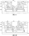
- FIGS. 4A-4G show an example of a technique of making a BBUL substrate with two die electrically coupled through a high density interconnect.
- FIGS. 5A-5E show an example of another technique of making a BBUL substrate with two die electrically coupled through a high density interconnect.
- FIGS. 6A-6E show an example of another technique of making a BBUL substrate with two die electrically coupled through a high density interconnect.
- FIG. 7 shows a block diagram example of an electronic device which can include a BBUL substrate with two die electrically coupled through a high density interconnect.
- a device can include a bumpless buildup layer (BBUL) substrate including a first die at least partially embedded in the BBUL substrate, the first die including a first plurality of high density interconnect pads.
- a second die can be at least partially embedded in the BBUL substrate, the second die including a second plurality of high density interconnect pads.
- a high density interconnect element can be embedded in the BBUL substrate, the high density interconnect element including a third plurality of high density interconnect pads electrically coupled to the first and second plurality of high density interconnect pads
- the input/output (IO) density in a package substrate can be a function of a substrate's minimum pad size, minimum trace dimensions, minimum space dimensions, or the capability of the manufacturing process.
- the routing density in a multichip substrate can be several orders of magnitude lower than chip level routing density. This routing density can impact cost, size, and performance of a product.
- a way to reduce the size of a product can include utilizing a silicon interposer in a package to provide a high density chip to chip interconnection.
- Such a solution can include a higher cost due to the cost of the silicon interposer, additional assembly and process steps, and compounding yield loss.
- a substrate can include a high density interconnect bridge in a BBUL package or substrate with multiple embedded dice (e.g., chips) embedded, at least partially, therein.
- a solution can eliminate a first level interconnect (FLI) die attach and use panel processing to reduce the overall cost.
- FLI first level interconnect
- Such a solution can allow a high density interconnect to be situated where it would be advantageous and allow low density interconnect (e.g., routing with a substrate routing technique) where it is desired.
- Substrate routing can take up a significant amount of space and can be a factor in the overall size of a die package. By including typical substrate routing techniques, which can result in less dense routing than chip routing techniques, there may not be enough space to route the die without routing through the die. Integrating a high density interconnect element in a package or substrate, such as a BBUL, package or substrate, can allow for an increase in overall local routing and interconnect density of a package, thus helping to reduce size and cost. These problems may be avoided by including a high density interconnect element in the substrate.
- the high density interconnect element is a silicon die interconnect bridge.
- the high density interconnect element is a glass die interconnect bridge.
- the high density interconnect element is a different type of chip made using chip routing technology.
- a BBUL package 100 with multiple embedded dice 102 A-B can include low density substrate routing (e.g., routing accomplished using a substrate routing technique) and low density interconnect pads 104 A-B (e.g., low density chip interconnects).
- the dice 102 A-B can be electrically coupled through low density interconnect pads 104 A-B that are electrically coupled through vias 106 A-B which are electrically coupled through another low density interconnect pad 104 C.
- Such an implementation can include up to about 23 interconnects/mm/layer.
- FIG. 2 shows an example of a BBUL substrate 200 with two dice 102 A-B electrically coupled through a high density interconnect element 114 .
- Each dice 102 A-B can include a plurality of low density interconnect pads 104 A-B, respectively, and a plurality a high density interconnect pads 116 A-B, respectively.
- the high density interconnect pads 116 A-B can be electrically coupled through high density interconnect pads 116 C-D on the high density interconnect element 114 .
- the high density interconnect element 114 can be routed to electrically couple a high density interconnect pad 116 A on die 102 A to a high density interconnect pad 116 B on second die 102 B.
- Such electrical coupling can be accomplished by coupling a high density interconnect pad 116 B to a high density interconnect pad 116 C, coupling the high density interconnect pad 116 C to another high density interconnect pad 116 D through a trace 107 in the high density interconnect element 114 , and coupling the high density interconnect pad 116 D to a high density interconnect pad 116 A on the die 102 A, such as shown in FIG. 3 .
- Such an implementation can include up to about 250 interconnects/mm/Layer.
- the dice 102 A-B can be analog or logic dice, or a mixture of analog and logic dice.
- An analog die is one that includes mostly analog components and a digital die is one that includes mostly logic gates and other logic components.
- the dice 102 A-B can include a CPU, graphics, memory, radio, MicroElectroMechanical system (MEMS) sensor, or other type of circuitry.
- MEMS MicroElectroMechanical system
- the BBUL substrate 200 can include a plurality of vias 106 electrically coupling low density interconnect pads 104 between buildup layers 108 A-D.
- the buildup layers 108 can include copper (Cu) interconnects and Ajinomoto dielectric buildup layers.
- the BBUL substrate can include a solder resist 112 situated on a fourth buildup layer 108 D and between solder balls 110 , or other electrically conductive interconnect elements.
- FIGS. 4A-4G show a technique for embedding a high density interconnect element 114 in a BBUL substrate or package.
- a substrate carrier 120 such as a coreless carrier or a copper substrate carrier, can be formed.
- Die backside films 122 A-B can be situated on a substrate carrier 120 .
- the die backside films 122 A-B can be situated using a dielectric lamination process.
- Dice 102 A-B can be situated on the die backside films 122 A-B, respectively.
- a silicide can be formed on the substrate carrier 120 or the die 102 and the die 102 can be coupled to the substrate carrier 120 through the silicide.
- an adhesive film is situated on a panel, the adhesive film is patterned to match a dice 102 footprint, and then dice 102 are situated on the adhesive film.
- FIG. 4D shows the via holes 124 at least partially filled with a conductive material, such as copper, to form electrically conductive vias 106 .
- Low density interconnect pads 104 C can be situated on or over the vias 106 .
- One or more of the low density interconnect pads 104 C can electrically couple two or more of the low density interconnect pads 104 A or 104 B, such as shown in FIG. 4D .
- the via holes 124 can be filled and the low density interconnect pads 104 C can be formed using a semi-additive lithographic or electroplating process.
- the low density interconnect pads 104 C-E can act as a bus, such as a power, ground, or data bus.
- a cavity 128 A can be formed in the buildup layer 108 A, such as to expose high density interconnect pads 116 A-B, such as shown in FIG. 4E .
- the cavity 128 is between about 30 um and 150 um deep with a length of up to about 10 mm and a width of up to about 10 mm. Other length, width, and depth dimensions are possible.
- FIG. 4F shows a high density interconnect element 114 situated at least partially in the cavity 128 A.
- the high density interconnect pads 1160 can be electrically coupled to the high density interconnect pads 116 A-B, such as shown in FIG. 4F .
- Such an electrical coupling can be created by depositing an epoxy flux and Thermal Compression Bonding (TCB) high density interconnect pads 116 C to high density interconnect pads 116 A-B (e.g., in situ epoxy TCB).
- TCB Thermal Compression Bonding
- Another technique of such electrical coupling includes using a TCB process to electrically couple high density interconnect pads 116 C to high density interconnect pads 116 A-B and filling gaps between the high density interconnect element 114 and the dice 102 A-B and between high density interconnect pads 116 A-C (e.g., in situ capillary underfill TCB).
- the technique can include removing contaminants, such as oxide, before TCB.
- FIG. 4G shows second and third buildup layers 108 B-C with vias 106 formed therein and low density interconnect pads 104 D-E formed thereon.
- a layer of solder resist 112 can be formed on the third buildup layer 108 C.
- the solder resist 112 can be situated so as to leave low density interconnect pads 104 E exposed.
- Solder balls 110 can be formed on the low density interconnect pads 104 E and the substrate carrier 120 can be removed.
- the resulting package can be similar to the BBUL substrate 200 , depicted in FIG. 2 .
- FIGS. 5A-5E depict a technique for embedding a high density interconnect element 114 in a BBUL substrate or package.
- the technique can begin with a process substantially similar to the process shown in FIGS. 4A-4D .
- FIG. 5A depicts the partial substrate of FIG. 4D with second and third buildup layers 108 B-C formed over the first buildup layer 108 A.
- the second and third buildup layers 108 B-C can include vias 106 formed therein and low density interconnect pads 104 D-E formed thereon.
- a layer of solder resist 112 can be formed on the third buildup layer 108 C, such as shown in FIG. 5A .
- a cavity 128 B can be formed by removing a portion of the solder resist 112 , first buildup layer 108 A, second buildup layer 108 B, and third buildup layer 108 C, such as cavity 128 B shown in FIG. 5B .
- Such a process can expose high density interconnect pads 116 A-B.
- Removing the portion of the solder resist 112 , first buildup layer 108 A, second buildup layer 108 B, and third buildup layer 108 C can be accomplished using a sandblasting or laser ablation process.
- the sandblasting can include dry film resist patterning with an optional etch stop at a passivation layer of the high density interconnect pads 116 A-B or the dice 102 .
- the laser ablation can include laser skiving, laser projection printing, or laser pulsing.
- sandblasting or laser ablation can be used to remove a majority of material to be removed (e.g., portions of one or more buildup layers or solder resist) and a selective etch (e.g., plasma ashing, wet etching, microwave plasma etching) can be used to remove the remainder of the material to be removed.
- a selective etch e.g., plasma ashing, wet etching, microwave plasma etching
- a high density interconnect element 114 can be situated in the cavity 128 , such as to electrically couple the dice 102 A-B.
- the high density interconnect element 114 can be coupled using an in situ epoxy TCB, an in situ capillary underfill TCB process, a solder ball attachment, or other process, such as shown in FIG. 5C .
- An encapsulant 126 e.g., mold material, ajinomoto dielectric film (ABF), or epoxy, among others
- AMF ajinomoto dielectric film
- Portions of solder resist 112 covering low density interconnect pads 104 E on the third buildup layer 108 C can be removed.
- FIG. 5E shows the substrate depicted in FIG. 5D with solder balls 110 electrically coupled to low density interconnect pads 104 E and the substrate carrier 120 removed.
- FIGS. 6A-6E depict a technique of situating a high density interconnect element 114 in a BBUL substrate or package.
- the technique can begin with the partial substrate depicted in FIG. 4A .
- a first build layer 108 A can be formed around the dice 102 A-B and over or on the substrate carrier 120 .
- the first buildup layer 108 A can leave the low density interconnect pads 104 A-B and the high density interconnect pads 116 A-B exposed.
- a high density interconnect element 114 can be electrically coupled to the dice 102 A-B, such as by using an in situ epoxy TCB or in situ capillary underfill TCB process, such as shown in FIG. 6A .
- FIG. 6B shows a second buildup layer 108 B formed on or over the first buildup layer 108 A and around the high density interconnect element 114 , the low density interconnect pads 104 A-B, and the dielectric 118 (e.g., epoxy or capillary underfill). Via holes 124 can be formed in the second buildup layer 108 B to expose low density interconnect pads 104 A-B, such as shown in FIG. 6C .
- the dielectric 118 e.g., epoxy or capillary underfill
- FIG. 6C shows the via holes 124 at least partially filled with a conductive material, such as copper, to form electrically conductive vias 106 .
- Low density interconnect pads 104 C can be situated on or over the vias 106 .
- FIG. 6D shows third and fourth buildup layers 108 C-D formed over the second buildup layer 1089 and vias 106 formed the third and fourth buildup layers 108 C-D.
- Low density interconnect pads 104 D-E can be formed on the third and fourth buildup layers 108 C-D, respectively.
- a layer of solder resist 112 can be formed on the fourth buildup layer 108 D. Portions of solder resist 112 can be removed to expose one or more low density interconnect pads 104 E.
- Solder balls 110 can be formed on the low density interconnect pads 104 E and the substrate carrier 120 can be removed.
- the resulting package can be similar to the BBUL substrate 200 , depicted in FIG. 2 .
- FIG. 7 shows an example of an electronic device 700 incorporating one or more high density interconnect element(s) 114 .
- Electronic device 700 is merely one example of a device in which embodiments of the present disclosure can be used. Examples of electronic devices 700 include, but are not limited to, personal computers, tablet computers, supercomputers, servers, telecommunications switches, routers, mobile telephones, personal data assistants, MP3 or other digital music players, radios, etc.
- electronic device 700 comprises a data processing system that includes a system bus 702 to couple the various components of the system.
- System bus 702 provides communications links among the various components of the electronic device 700 and can be implemented as a single bus, as a combination of busses, or in any other suitable manner.
- An electronic assembly 710 is coupled to system bus 702 .
- the electronic assembly 710 can include a circuit or combination of circuits.
- the electronic assembly 710 includes a processor 712 which can be of any type.
- processor means any type of computational circuit, such as but not limited to a microprocessor, a microcontroller, a complex instruction set computing (CISC) microprocessor, a reduced instruction set computing (RISC) microprocessor, a very long instruction word (VLIW) microprocessor, a graphics processor, a digital signal processor (DSP), multiple core processor, or any other type of processor or processing circuit.
- CISC complex instruction set computing
- RISC reduced instruction set computing
- VLIW very long instruction word
- DSP digital signal processor
- circuits that can be included in electronic assembly 710 are a custom circuit, an application-specific integrated circuit (ASIC), or the like, such as, for example, one or more circuits (such as a communications circuit 714 ) for use in wireless devices like mobile telephones, pagers, personal data assistants, portable computers, two-way radios, and similar electronic systems.
- ASIC application-specific integrated circuit
- the IC can perform any other type of function.
- the electronic device 700 can include an external memory 720 , which in turn can include one or more memory elements suitable to the particular application, such as a main memory 722 in the form of random access memory (RAM), one or more hard drives 724 , and/or one or more drives that handle removable media 726 such as compact disks (CD), digital video disk (DVD), and the like.
- RAM random access memory
- CD compact disks
- DVD digital video disk
- the electronic device 700 can also include a display device 716 , one or more speakers 718 , and a keyboard and/or controller 730 , which can include a mouse, trackball, touch screen, voice-recognition device, or any other device that permits a system user to input information into and receive information from the electronic device 700 .
- Example 2 the method of Example 1 includes situating a second die including a second plurality of high density interconnect pads on the substrate carrier.
- Example 3 the method of at least one of Examples 1-2 includes forming a first buildup layer around and over the first and second dies.
- Example 5 the method of at least one of Examples 1-4 includes situating the high density interconnect element in the cavity.
- Example 6 situating first and second dice of at least one of Examples 1-5 includes situating a first die including a first plurality of low density interconnect pads and a second die including a second plurality of low density interconnect pads on the substrate carrier.
- Example 8 the method of at least one of Examples 1-7 includes at least partially filling the first plurality of via holes in the first buildup layer with conductive material.
- Example 10 the method of at least one of Examples 1-9 includes forming a second buildup layer on the first buildup layer and the third set of low density interconnect pads.
- Example 11 the method of at least one of Examples 1-10 includes forming a second plurality of via holes in the second buildup layer;
- Example 12 the method of at least one of Examples 1-11 includes at least partially filling the second plurality of via holes in the second buildup layer with conductive material.
- Example 14 the method of at least one of Examples 1-13 includes situating solder resist over the second buildup layer.
- Example 15 the method of at least one of Examples 1-14 includes forming solder balls on the fourth plurality of low density interconnect pads.
- Example 16 forming the cavity in the buildup layer of at least one of Examples 1-15 includes sandblasting or laser ablating the buildup layer.
- Example 17 the method of at least one of Examples 1-16 includes filling the cavity with encapsulant.
- Example 18 situating the high density interconnect element in the cavity of at least one of Examples 1-17 includes electrically coupling high density interconnect pads on the high density interconnect element to the first and second pluralities of high density interconnect pads using an in situ capillary underfill or an in situ epoxy thermal compression bonding process.
- a method of making a BBUL substrate with a high density interconnect element embedded therein includes situating a first die including a first plurality of high density interconnect pads on a substrate carrier.
- Example 20 the method of at least one of Examples 1-19 includes situating a second die including a second plurality of high density interconnect pads on the substrate carrier.
- the method of at least one of Examples 1-20 includes forming a first buildup layer around the first and second die and on the substrate carrier.
- Example 22 the method of at least one of Examples 1-21 includes situating the high density interconnect element on the first and second pluralities of high density interconnect pads.
- Example 23 the method of at least one of Examples 1-22 includes forming a second buildup layer over the first die, second die, and the first buildup layer.
- Example 24 the method of at least one of Examples 1-23 includes forming a first plurality of via holes in the second buildup layer.
- Example 25 the method of at least one of Examples 1-24 includes at least partially filling the first plurality of via holes with conductive material.
- Example 26 the method of at least one of Examples 1-25 includes forming a third plurality of low density interconnect pads over the at least partially filled first plurality of via holes.
- Example 27 the method of at least one of Examples 1-26 includes situating solder resist over the second buildup layer and around the third plurality of low density interconnect pads.
- Example 28 the method of at least one of Examples 1-27 includes forming solder balls on the third plurality of low density interconnect pads.
- Example 29 at least partially filling the first plurality of via holes with conductive material of at least one of Examples 1-28 includes at least partially filling the first plurality of via holes with copper.
- the method of at least one of Examples 1-29 includes removing the substrate carrier.
- Example 31 situating the high density interconnect element on the first and second pluralities of high density interconnect pads of at least one of Examples 1-32 includes electrically coupling high density interconnect pads on the high density interconnect element to the first and second dice using an in situ capillary underfill or an in situ epoxy thermal compression bonding process.
- a device including a bumpless buildup layer (BBUL) substrate includes a first die at least partially embedded in the BBUL substrate, the first die including a first plurality of high density interconnect pads.
- BBUL bumpless buildup layer
- Example 34 the device of at least one of Examples 1-33 includes a high density interconnect element embedded in the BBUL substrate, the high density interconnect element including a third plurality of high density interconnect pads electrically coupled to the first and second plurality of high density interconnect pads.
- Example 35 the device of at least one of Examples 1-34 includes encapsulant on the high density interconnect element.
- Example 36 the device of at least one of Examples 1-35 includes at least one buildup layer formed over the high density interconnect element.
- first and second die of at least one of Examples 1-36 are a logic die and an analog die, respectively.
- Example 38 the high density interconnect element of at least one of Examples 1-37 is a silicon die interconnect bridge or a glass die interconnect bridge.
- Example 39 the first die of at least one of Examples 1-38 includes a plurality of low density interconnect pads electrically connected to a bus of the BBUL substrate.
- Example 40 the second die of at least one of Examples 1-39 includes a plurality of low density interconnect pads electrically connected to the bus of the BBUL substrate.
- Example 41 the bus of at least one of Examples 1-40 is a power bus or a ground bus.
Abstract
Description
Claims (19)
Priority Applications (4)
| Application Number | Priority Date | Filing Date | Title |
|---|---|---|---|
| US16/561,965 US10861815B2 (en) | 2012-12-06 | 2019-09-05 | High density substrate routing in package |
| US17/077,996 US11251150B2 (en) | 2012-12-06 | 2020-10-22 | High density substrate routing in package |
| US17/570,255 US11810884B2 (en) | 2012-12-06 | 2022-01-06 | High density substrate routing in package |
| US18/373,849 US20240021562A1 (en) | 2012-12-06 | 2023-09-27 | High density substrate routing in package |
Applications Claiming Priority (7)
| Application Number | Priority Date | Filing Date | Title |
|---|---|---|---|
| US13/707,159 US9190380B2 (en) | 2012-12-06 | 2012-12-06 | High density substrate routing in BBUL package |
| US14/663,689 US9171816B2 (en) | 2012-12-06 | 2015-03-20 | High density substrate routing in BBUL package |
| US14/922,425 US9437569B2 (en) | 2012-12-06 | 2015-10-26 | High density substrate routing in BBUL package |
| US15/255,351 US9929119B2 (en) | 2012-12-06 | 2016-09-02 | High density substrate routing in BBUL package |
| US15/873,567 US10199346B2 (en) | 2012-12-06 | 2018-01-17 | High density substrate routing in package |
| US16/239,670 US10438915B2 (en) | 2012-12-06 | 2019-01-04 | High density substrate routing in package |
| US16/561,965 US10861815B2 (en) | 2012-12-06 | 2019-09-05 | High density substrate routing in package |
Related Parent Applications (1)
| Application Number | Title | Priority Date | Filing Date |
|---|---|---|---|
| US16/239,670 Continuation US10438915B2 (en) | 2012-12-06 | 2019-01-04 | High density substrate routing in package |
Related Child Applications (1)
| Application Number | Title | Priority Date | Filing Date |
|---|---|---|---|
| US17/077,996 Continuation US11251150B2 (en) | 2012-12-06 | 2020-10-22 | High density substrate routing in package |
Publications (2)
| Publication Number | Publication Date |
|---|---|
| US20190393180A1 US20190393180A1 (en) | 2019-12-26 |
| US10861815B2 true US10861815B2 (en) | 2020-12-08 |
Family
ID=50880069
Family Applications (10)
| Application Number | Title | Priority Date | Filing Date |
|---|---|---|---|
| US13/707,159 Active US9190380B2 (en) | 2012-12-06 | 2012-12-06 | High density substrate routing in BBUL package |
| US14/663,689 Active US9171816B2 (en) | 2012-12-06 | 2015-03-20 | High density substrate routing in BBUL package |
| US14/922,425 Active US9437569B2 (en) | 2012-12-06 | 2015-10-26 | High density substrate routing in BBUL package |
| US15/255,351 Active US9929119B2 (en) | 2012-12-06 | 2016-09-02 | High density substrate routing in BBUL package |
| US15/873,567 Active US10199346B2 (en) | 2012-12-06 | 2018-01-17 | High density substrate routing in package |
| US16/239,670 Active US10438915B2 (en) | 2012-12-06 | 2019-01-04 | High density substrate routing in package |
| US16/561,965 Active US10861815B2 (en) | 2012-12-06 | 2019-09-05 | High density substrate routing in package |
| US17/077,996 Active US11251150B2 (en) | 2012-12-06 | 2020-10-22 | High density substrate routing in package |
| US17/570,255 Active US11810884B2 (en) | 2012-12-06 | 2022-01-06 | High density substrate routing in package |
| US18/373,849 Pending US20240021562A1 (en) | 2012-12-06 | 2023-09-27 | High density substrate routing in package |
Family Applications Before (6)
| Application Number | Title | Priority Date | Filing Date |
|---|---|---|---|
| US13/707,159 Active US9190380B2 (en) | 2012-12-06 | 2012-12-06 | High density substrate routing in BBUL package |
| US14/663,689 Active US9171816B2 (en) | 2012-12-06 | 2015-03-20 | High density substrate routing in BBUL package |
| US14/922,425 Active US9437569B2 (en) | 2012-12-06 | 2015-10-26 | High density substrate routing in BBUL package |
| US15/255,351 Active US9929119B2 (en) | 2012-12-06 | 2016-09-02 | High density substrate routing in BBUL package |
| US15/873,567 Active US10199346B2 (en) | 2012-12-06 | 2018-01-17 | High density substrate routing in package |
| US16/239,670 Active US10438915B2 (en) | 2012-12-06 | 2019-01-04 | High density substrate routing in package |
Family Applications After (3)
| Application Number | Title | Priority Date | Filing Date |
|---|---|---|---|
| US17/077,996 Active US11251150B2 (en) | 2012-12-06 | 2020-10-22 | High density substrate routing in package |
| US17/570,255 Active US11810884B2 (en) | 2012-12-06 | 2022-01-06 | High density substrate routing in package |
| US18/373,849 Pending US20240021562A1 (en) | 2012-12-06 | 2023-09-27 | High density substrate routing in package |
Country Status (1)
| Country | Link |
|---|---|
| US (10) | US9190380B2 (en) |
Families Citing this family (78)
| Publication number | Priority date | Publication date | Assignee | Title |
|---|---|---|---|---|
| WO2013089754A1 (en) * | 2011-12-15 | 2013-06-20 | Intel Corporation | Packaged semiconductor die with bumpless die-package interface for bumpless build-up layer (bbul) packages |
| US9136236B2 (en) | 2012-09-28 | 2015-09-15 | Intel Corporation | Localized high density substrate routing |
| US9190380B2 (en) | 2012-12-06 | 2015-11-17 | Intel Corporation | High density substrate routing in BBUL package |
| US8866308B2 (en) | 2012-12-20 | 2014-10-21 | Intel Corporation | High density interconnect device and method |
| US8901748B2 (en) * | 2013-03-14 | 2014-12-02 | Intel Corporation | Direct external interconnect for embedded interconnect bridge package |
| US9312233B2 (en) * | 2013-06-27 | 2016-04-12 | Intel Corporation | Method of forming molded panel embedded die structure |
| US9041205B2 (en) * | 2013-06-28 | 2015-05-26 | Intel Corporation | Reliable microstrip routing for electronics components |
| US9159690B2 (en) | 2013-09-25 | 2015-10-13 | Intel Corporation | Tall solders for through-mold interconnect |
| US9349703B2 (en) | 2013-09-25 | 2016-05-24 | Intel Corporation | Method for making high density substrate interconnect using inkjet printing |
| US9242854B2 (en) | 2013-12-20 | 2016-01-26 | Intel Corporation | Hermetic encapsulation for microelectromechanical systems (MEMS) devices |
| US20150255411A1 (en) * | 2014-03-05 | 2015-09-10 | Omkar G. Karhade | Die-to-die bonding and associated package configurations |
| US9275975B2 (en) * | 2014-03-28 | 2016-03-01 | Intel Corporation | Electronic package and method of connecting a first die to a second die to form an electronic package |
| CN105684146B (en) * | 2014-07-28 | 2019-01-18 | 英特尔公司 | Multi-chip module semiconductor chip packaging with dense pack wiring |
| US9666559B2 (en) | 2014-09-05 | 2017-05-30 | Invensas Corporation | Multichip modules and methods of fabrication |
| US9595496B2 (en) * | 2014-11-07 | 2017-03-14 | Qualcomm Incorporated | Integrated device package comprising silicon bridge in an encapsulation layer |
| US11069734B2 (en) | 2014-12-11 | 2021-07-20 | Invensas Corporation | Image sensor device |
| US9368450B1 (en) * | 2015-08-21 | 2016-06-14 | Qualcomm Incorporated | Integrated device package comprising bridge in litho-etchable layer |
| US10692847B2 (en) * | 2015-08-31 | 2020-06-23 | Intel Corporation | Inorganic interposer for multi-chip packaging |
| US9543249B1 (en) * | 2015-09-21 | 2017-01-10 | Dyi-chung Hu | Package substrate with lateral communication circuitry |
| US20170092594A1 (en) * | 2015-09-25 | 2017-03-30 | Qualcomm Incorporated | Low profile package with passive device |
| US9818659B2 (en) * | 2015-10-12 | 2017-11-14 | Deca Technologies Inc. | Multi-die package comprising unit specific alignment and unit specific routing |
| US10438881B2 (en) * | 2015-10-29 | 2019-10-08 | Marvell World Trade Ltd. | Packaging arrangements including high density interconnect bridge |
| US10163856B2 (en) | 2015-10-30 | 2018-12-25 | Taiwan Semiconductor Manufacturing Company, Ltd. | Stacked integrated circuit structure and method of forming |
| WO2017095419A1 (en) | 2015-12-03 | 2017-06-08 | Intel Corporation | A hybrid microelectronic substrate and methods for fabricating the same |
| CN108369944B (en) | 2015-12-09 | 2022-11-22 | 英特尔公司 | Hybrid microelectronic substrate and method for manufacturing the same |
| US10418329B2 (en) | 2015-12-11 | 2019-09-17 | Intel Corporation | Microelectronic structures having multiple microelectronic devices connected with a microelectronic bridge embedded in a microelectronic substrate |
| TWI652778B (en) * | 2016-01-27 | 2019-03-01 | 艾馬克科技公司 | Semiconductor package and method of manufacturing same |
| US9633950B1 (en) * | 2016-02-10 | 2017-04-25 | Qualcomm Incorporated | Integrated device comprising flexible connector between integrated circuit (IC) packages |
| US9935009B2 (en) * | 2016-03-30 | 2018-04-03 | International Business Machines Corporation | IR assisted fan-out wafer level packaging using silicon handler |
| US10276403B2 (en) * | 2016-06-15 | 2019-04-30 | Avago Technologies International Sales Pe. Limited | High density redistribution layer (RDL) interconnect bridge using a reconstituted wafer |
| US11094633B2 (en) | 2016-06-30 | 2021-08-17 | Intel Corporation | Bridge die design for high bandwidth memory interface |
| WO2018009145A1 (en) * | 2016-07-08 | 2018-01-11 | Agency For Science, Technology And Research | A semiconductor package and methods of forming the same |
| KR102632563B1 (en) | 2016-08-05 | 2024-02-02 | 삼성전자주식회사 | Semiconductor Package |
| KR102595896B1 (en) * | 2016-08-08 | 2023-10-30 | 삼성전자 주식회사 | Printed Circuit Board, and semiconductor package having the same |
| DE112016007150T5 (en) | 2016-08-16 | 2019-05-02 | Intel Corporation | ROUNDED METAL-LADDER RAILWAY CORNER FOR VOLTAGE REDUCTION |
| WO2018063263A1 (en) | 2016-09-29 | 2018-04-05 | Intel Corporation | Panel level packaging for multi-die products interconnected with very high density (vhd) interconnect layers |
| US20180096938A1 (en) * | 2016-09-30 | 2018-04-05 | Advanced Micro Devices, Inc. | Circuit board with multiple density regions |
| US11277922B2 (en) * | 2016-10-06 | 2022-03-15 | Advanced Micro Devices, Inc. | Circuit board with bridge chiplets |
| KR20180070786A (en) * | 2016-12-16 | 2018-06-27 | 삼성전자주식회사 | Semiconductor package |
| CN110024117B (en) * | 2016-12-29 | 2023-07-21 | 英特尔公司 | Bare die intelligent bridge connected with copper column for system-in-package equipment |
| KR20180086804A (en) * | 2017-01-23 | 2018-08-01 | 앰코 테크놀로지 인코포레이티드 | Semiconductor device and manufacturing method thereof |
| EP3373714B1 (en) * | 2017-03-08 | 2023-08-23 | AT & S Austria Technologie & Systemtechnik Aktiengesellschaft | Hybrid component carrier and method for manufacturing the same |
| WO2018182658A1 (en) * | 2017-03-31 | 2018-10-04 | Intel Corporation | A die interconnect substrate, an electrical device, and a method for forming a die interconnect substrate |
| WO2018182659A1 (en) * | 2017-03-31 | 2018-10-04 | Intel Corporation | A die interconnect substrate, an electrical device and a method for forming a die interconnect substrate |
| US10403599B2 (en) | 2017-04-27 | 2019-09-03 | Invensas Corporation | Embedded organic interposers for high bandwidth |
| KR102366970B1 (en) * | 2017-05-16 | 2022-02-24 | 삼성전자주식회사 | Semiconductor package |
| US10217720B2 (en) | 2017-06-15 | 2019-02-26 | Invensas Corporation | Multi-chip modules formed using wafer-level processing of a reconstitute wafer |
| US10290611B2 (en) | 2017-07-27 | 2019-05-14 | Taiwan Semiconductor Manufacturing Company, Ltd. | Semiconductor packages and methods of forming same |
| CN109309043B (en) * | 2017-07-27 | 2021-03-09 | 中芯国际集成电路制造(上海)有限公司 | Semiconductor structure and forming method thereof |
| US10510721B2 (en) * | 2017-08-11 | 2019-12-17 | Advanced Micro Devices, Inc. | Molded chip combination |
| US10361158B2 (en) * | 2017-08-29 | 2019-07-23 | Micron Technology, Inc. | Integrated assemblies having structures along a first pitch coupled with structures along a second pitch different from the first pitch |
| US10475736B2 (en) | 2017-09-28 | 2019-11-12 | Intel Corporation | Via architecture for increased density interface |
| US11145632B2 (en) | 2017-09-29 | 2021-10-12 | Intel Corporation | High density die package configuration on system boards |
| EP3688800A4 (en) | 2017-09-29 | 2021-05-19 | INTEL Corporation | Horizontal pitch translation using embedded bridge dies |
| TWI652788B (en) * | 2017-11-09 | 2019-03-01 | 大陸商上海兆芯集成電路有限公司 | Chip package structure and chip package structure array |
| US10163798B1 (en) * | 2017-12-22 | 2018-12-25 | Intel Corporation | Embedded multi-die interconnect bridge packages with lithotgraphically formed bumps and methods of assembling same |
| KR102505437B1 (en) * | 2017-12-26 | 2023-03-03 | 삼성전기주식회사 | Wire wound inductor and manufacturing method thereof |
| US11735570B2 (en) * | 2018-04-04 | 2023-08-22 | Intel Corporation | Fan out packaging pop mechanical attach method |
| US10593628B2 (en) | 2018-04-24 | 2020-03-17 | Advanced Micro Devices, Inc. | Molded die last chip combination |
| US10622321B2 (en) * | 2018-05-30 | 2020-04-14 | Taiwan Semiconductor Manufacturing Co., Ltd. | Semiconductor structures and methods of forming the same |
| US10916519B2 (en) | 2018-06-08 | 2021-02-09 | Taiwan Semiconductor Manufacturing Company, Ltd. | Method for manufacturing semiconductor package with connection structures including via groups |
| US11462419B2 (en) | 2018-07-06 | 2022-10-04 | Invensas Bonding Technologies, Inc. | Microelectronic assemblies |
| US20200035591A1 (en) * | 2018-07-30 | 2020-01-30 | Dyi-chung Hu | Interposer and manufacturing method thereof |
| CN111372369B (en) | 2018-12-25 | 2023-07-07 | 奥特斯科技(重庆)有限公司 | Component carrier with component shielding and method for producing the same |
| US11769735B2 (en) * | 2019-02-12 | 2023-09-26 | Intel Corporation | Chiplet first architecture for die tiling applications |
| US10985101B2 (en) * | 2019-03-14 | 2021-04-20 | Taiwan Semiconductor Manufacturing Company, Ltd. | Semiconductor package and manufacturing method thereof |
| US11296053B2 (en) | 2019-06-26 | 2022-04-05 | Invensas Bonding Technologies, Inc. | Direct bonded stack structures for increased reliability and improved yield in microelectronics |
| US10923430B2 (en) | 2019-06-30 | 2021-02-16 | Advanced Micro Devices, Inc. | High density cross link die with polymer routing layer |
| CN112652608A (en) | 2019-10-09 | 2021-04-13 | 财团法人工业技术研究院 | Multi-chip package and manufacturing method thereof |
| US11587905B2 (en) | 2019-10-09 | 2023-02-21 | Industrial Technology Research Institute | Multi-chip package and manufacturing method thereof |
| TWI701777B (en) | 2019-10-22 | 2020-08-11 | 財團法人工業技術研究院 | Image sensor package and manufacture method thereof |
| CN111554676B (en) * | 2020-05-19 | 2022-03-29 | 上海先方半导体有限公司 | Interposer packaging structure with enhanced local bandwidth and manufacturing method thereof |
| US11631647B2 (en) | 2020-06-30 | 2023-04-18 | Adeia Semiconductor Bonding Technologies Inc. | Integrated device packages with integrated device die and dummy element |
| US11764177B2 (en) | 2020-09-04 | 2023-09-19 | Adeia Semiconductor Bonding Technologies Inc. | Bonded structure with interconnect structure |
| US11728273B2 (en) | 2020-09-04 | 2023-08-15 | Adeia Semiconductor Bonding Technologies Inc. | Bonded structure with interconnect structure |
| WO2022153433A1 (en) * | 2021-01-14 | 2022-07-21 | 昭和電工マテリアルズ株式会社 | Method for manufacturing wiring-layer-equipped board, wiring-layer-equipped board, method for manufacturing semiconductor device, and semiconductor device |
| US20230035627A1 (en) * | 2021-07-27 | 2023-02-02 | Qualcomm Incorporated | Split die integrated circuit (ic) packages employing die-to-die (d2d) connections in die-substrate standoff cavity, and related fabrication methods |
| CN113643986B (en) * | 2021-08-10 | 2024-04-09 | 中国科学院微电子研究所 | Manufacturing method of structure for improving interconnection precision between embedded silicon bridge and chip |
Citations (112)
| Publication number | Priority date | Publication date | Assignee | Title |
|---|---|---|---|---|
| US5102829A (en) | 1991-07-22 | 1992-04-07 | At&T Bell Laboratories | Plastic pin grid array package |
| US5111278A (en) | 1991-03-27 | 1992-05-05 | Eichelberger Charles W | Three-dimensional multichip module systems |
| US5227013A (en) | 1991-07-25 | 1993-07-13 | Microelectronics And Computer Technology Corporation | Forming via holes in a multilevel substrate in a single step |
| US5241456A (en) * | 1990-07-02 | 1993-08-31 | General Electric Company | Compact high density interconnect structure |
| US5285352A (en) | 1992-07-15 | 1994-02-08 | Motorola, Inc. | Pad array semiconductor device with thermal conductor and process for making the same |
| US5287247A (en) | 1990-09-21 | 1994-02-15 | Lsi Logic Corporation | Computer system module assembly |
| US5497033A (en) | 1993-02-08 | 1996-03-05 | Martin Marietta Corporation | Embedded substrate for integrated circuit modules |
| US5664772A (en) * | 1994-11-04 | 1997-09-09 | Pitney Bowes Inc. | Apparatus and method for right angle turn over of sheet material |
| US5703400A (en) | 1995-12-04 | 1997-12-30 | General Electric Company | Fabrication and structures of two-sided molded circuit modules with flexible interconnect layers |
| US5745984A (en) | 1995-07-10 | 1998-05-05 | Martin Marietta Corporation | Method for making an electronic module |
| US5761044A (en) | 1995-02-14 | 1998-06-02 | Nec Corporation | Semiconductor module for microprocessor |
| TW343241B (en) | 1995-03-31 | 1998-10-21 | Nippon Seishi Kk | Recording paper |
| US5838545A (en) | 1996-10-17 | 1998-11-17 | International Business Machines Corporation | High performance, low cost multi-chip modle package |
| US5859474A (en) | 1997-04-23 | 1999-01-12 | Lsi Logic Corporation | Reflow ball grid array assembly |
| US5903052A (en) | 1998-05-12 | 1999-05-11 | Industrial Technology Research Institute | Structure for semiconductor package for improving the efficiency of spreading heat |
| US6011694A (en) | 1996-08-01 | 2000-01-04 | Fuji Machinery Mfg. & Electronics Co., Ltd. | Ball grid array semiconductor package with solder ball openings in an insulative base |
| US6084297A (en) | 1998-09-03 | 2000-07-04 | Micron Technology, Inc. | Cavity ball grid array apparatus |
| US6150716A (en) | 1995-01-25 | 2000-11-21 | International Business Machines Corporation | Metal substrate having an IC chip and carrier mounting |
| US6154366A (en) | 1999-11-23 | 2000-11-28 | Intel Corporation | Structures and processes for fabricating moisture resistant chip-on-flex packages |
| US6229203B1 (en) | 1997-03-12 | 2001-05-08 | General Electric Company | Semiconductor interconnect structure for high temperature applications |
| US20010005047A1 (en) | 1999-05-10 | 2001-06-28 | Jimarez Miguel Angel | Flip chip C4 extension structure and process |
| US6271469B1 (en) | 1999-11-12 | 2001-08-07 | Intel Corporation | Direct build-up layer on an encapsulated die package |
| WO2002015266A2 (en) | 2000-08-16 | 2002-02-21 | Intel Corporation | Direct build-up layer on an encapsulated die package |
| US20020070443A1 (en) | 2000-12-08 | 2002-06-13 | Xiao-Chun Mu | Microelectronic package having an integrated heat sink and build-up layers |
| US6495914B1 (en) | 1997-08-19 | 2002-12-17 | Hitachi, Ltd. | Multi-chip module structure having conductive blocks to provide electrical connection between conductors on first and second sides of a conductive base substrate |
| US6506632B1 (en) | 2002-02-15 | 2003-01-14 | Unimicron Technology Corp. | Method of forming IC package having downward-facing chip cavity |
| US6545351B1 (en) | 1998-07-21 | 2003-04-08 | Intel Corporation | Underside heat slug for ball grid array packages |
| US20030144405A1 (en) | 2000-04-04 | 2003-07-31 | Anke Lewin | Assembly adhesive on the basis of an aqueous polymer dispersion |
| US20030222344A1 (en) | 2002-05-30 | 2003-12-04 | Fujitsu Limited | Semiconductor device having a heat spreader exposed from a seal resin |
| JP2004111415A (en) | 2002-09-13 | 2004-04-08 | Sony Corp | Circuit board, its manufacturing method, semiconductor device, and its manufacturing method |
| TW200409324A (en) | 2002-11-29 | 2004-06-01 | Via Tech Inc | High-density multi-chip modulestructure and the forming method thereof |
| US20040173822A1 (en) | 2003-03-05 | 2004-09-09 | Achyut Dutta | High speed electronics interconnect and method of manufacture |
| US20050067688A1 (en) | 2003-09-26 | 2005-03-31 | Tessera, Inc. | Structure and method of making capped chips including vertical interconnects having stud bumps engaged to surfaces of said caps |
| US20050098891A1 (en) | 2002-02-04 | 2005-05-12 | Casio Computer Co., Ltd | Semiconductor device and method of manufacturing the same |
| US20050230835A1 (en) | 2004-04-20 | 2005-10-20 | Shinko Electric Industries Co., Ltd. | Semiconductor device |
| US6969640B1 (en) | 2004-09-02 | 2005-11-29 | Stats Chippac Ltd. | Air pocket resistant semiconductor package system |
| US20060038278A1 (en) | 2004-08-18 | 2006-02-23 | Chung-Cheng Wang | Submember mounted on a chip of electrical device for electrical connection |
| US20060046468A1 (en) | 2004-08-31 | 2006-03-02 | Salman Akram | Through-substrate interconnect fabrication methods and resulting structures and assemblies |
| US20060087036A1 (en) | 2004-10-26 | 2006-04-27 | Advanced Chip Engineering Technology Inc. | Chip-size package structure and method of the same |
| US7042081B2 (en) | 2003-09-19 | 2006-05-09 | Casio Computer Co., Ltd. | Semiconductor device having heat dissipation layer |
| US20060097379A1 (en) | 2004-11-10 | 2006-05-11 | Chung-Cheng Wang | Substrate for electrical device and methods for making the same |
| CN1835229A (en) | 2005-03-16 | 2006-09-20 | 索尼株式会社 | Semiconductor device and method of manufacturing semiconductor device |
| US20060286301A1 (en) | 2003-09-12 | 2006-12-21 | National Institute Of Advanced Industrial Science | Substrates and method of manufacturing same |
| US7189596B1 (en) | 2000-03-01 | 2007-03-13 | Intel Corporation | Process for forming a direct build-up layer on an encapsulated die packages utilizing intermediate structures |
| US20070114677A1 (en) | 2005-11-24 | 2007-05-24 | Samsung Electronics Co., Ltd. | Semiconductor package with heat sink, stack package using the same and manufacturing method thereof |
| US20070128855A1 (en) | 2005-12-07 | 2007-06-07 | Samsung Electro-Mechanics Co., Ltd. | Printed wiring board and method for manufacturing the same |
| US20070138644A1 (en) | 2005-12-15 | 2007-06-21 | Tessera, Inc. | Structure and method of making capped chip having discrete article assembled into vertical interconnect |
| US20070148819A1 (en) | 2005-12-23 | 2007-06-28 | Tessera, Inc. | Microelectronic assemblies having very fine pitch stacking |
| US20070145564A1 (en) | 2005-03-22 | 2007-06-28 | Tessera, Inc. | Sequential fabrication of vertical conductive interconnects in capped chips |
| US20070205496A1 (en) | 2004-06-25 | 2007-09-06 | Tessera, Inc. | Microelectronic packages and methods therefor |
| US20080017956A1 (en) | 2006-07-19 | 2008-01-24 | Taiwan Semiconductor Manufacturing Co., Ltd. | Interconnect structure for semiconductor package |
| US20080054448A1 (en) | 2006-09-01 | 2008-03-06 | Daoqiang Lu | Dual heat spreader panel assembly method for bumpless die-attach packages, packages containing same, and systems containing same |
| TWM343241U (en) | 2008-05-13 | 2008-10-21 | Silicon Motion Inc | Semiconductor chip package structure |
| US20080315398A1 (en) | 2007-06-22 | 2008-12-25 | Hsing-Lun Lo | Packaging substrate with embedded chip and buried heatsink |
| US20090045524A1 (en) | 2007-08-16 | 2009-02-19 | Tessera, Inc. | Microelectronic package |
| US20090089466A1 (en) | 2007-09-28 | 2009-04-02 | Sun Microsystems, Inc. | Proximity communication package for processor, cache and memory |
| US20090206455A1 (en) | 2008-02-19 | 2009-08-20 | Texas Instruments Incorporated | Integrated circuit stacked package precursors and stacked packaged devices and systems therefrom |
| US20090212407A1 (en) | 2005-05-12 | 2009-08-27 | Foster Ron B | Infinitely Stackable Interconnect Device and Method |
| US7659143B2 (en) | 2006-09-29 | 2010-02-09 | Intel Corporation | Dual-chip integrated heat spreader assembly, packages containing same, and systems containing same |
| US20100072598A1 (en) | 2008-09-19 | 2010-03-25 | Oh Jae Sung | Semiconductor package and stacked semiconductor package having the same |
| US20100072263A1 (en) | 2008-07-29 | 2010-03-25 | International Business Machines Corporation | Method and Apparatus for Forming Planar Alloy Deposits on a Substrate |
| US7777351B1 (en) | 2007-10-01 | 2010-08-17 | Amkor Technology, Inc. | Thin stacked interposer package |
| US7851905B2 (en) | 2007-09-26 | 2010-12-14 | Intel Corporation | Microelectronic package and method of cooling an interconnect feature in same |
| US7851894B1 (en) | 2008-12-23 | 2010-12-14 | Amkor Technology, Inc. | System and method for shielding of package on package (PoP) assemblies |
| CN101960589A (en) | 2008-03-31 | 2011-01-26 | 英特尔公司 | Microelectronic package containing silicon patches for high density interconnects, and method of manufacturing same |
| US7880489B2 (en) | 2008-11-04 | 2011-02-01 | Formfactor, Inc. | Printing of redistribution traces on electronic component |
| CN102148206A (en) | 2010-03-29 | 2011-08-10 | 日月光半导体制造股份有限公司 | Semiconductor packaging structure and producing method thereof |
| US20110210443A1 (en) | 2010-02-26 | 2011-09-01 | Xilinx, Inc. | Semiconductor device having bucket-shaped under-bump metallization and method of forming same |
| US8018072B1 (en) | 2008-12-23 | 2011-09-13 | Amkor Technology, Inc. | Semiconductor package having a heat spreader with an exposed exterion surface and a top mold gate |
| US20110227209A1 (en) | 2010-03-18 | 2011-09-22 | In Sang Yoon | Integrated circuit package system with package stacking and method of manufacture thereof |
| US20110228464A1 (en) | 2010-03-17 | 2011-09-22 | Guzek John S | System-in-package using embedded-die coreless substrates, and processes of forming same |
| KR20110123297A (en) | 2010-05-07 | 2011-11-15 | 주식회사 네패스 | Wafer level semiconductor package and fabrication method thereof |
| US8093704B2 (en) | 2008-06-03 | 2012-01-10 | Intel Corporation | Package on package using a bump-less build up layer (BBUL) package |
| KR20120014099A (en) | 2010-08-06 | 2012-02-16 | 타이완 세미콘덕터 매뉴팩쳐링 컴퍼니 리미티드 | Flip chip substrate package assembly and process for making same |
| DE102011053161A1 (en) | 2010-08-31 | 2012-03-29 | Infineon Technologies Ag | METHOD AND SYSTEM FOR LEADING ELECTRICAL CONNECTIONS OF SEMICONDUCTOR CHIPS |
| CN102460690A (en) | 2009-06-24 | 2012-05-16 | 英特尔公司 | Multi-chip package and method of providing die-to-die interconnects in same |
| US20120161331A1 (en) | 2010-12-22 | 2012-06-28 | Javier Soto Gonzalez | Multi-chip package having a substrate with a plurality of vertically embedded die and a process of forming the same |
| US8345441B1 (en) | 2011-10-03 | 2013-01-01 | Invensas Corporation | Stub minimization for multi-die wirebond assemblies with parallel windows |
| KR20130007049A (en) | 2011-06-28 | 2013-01-18 | 삼성전자주식회사 | Package on package using through silicon via technique |
| US20130105962A1 (en) * | 2007-03-29 | 2013-05-02 | Continental Automotive Systems, Inc. | Thermal dissipation in chip |
| US20130119536A1 (en) | 2011-11-15 | 2013-05-16 | International Business Machines Corporation | Method for forming studs used for self-alignment of solder bumps |
| US8461036B2 (en) * | 2009-12-22 | 2013-06-11 | Intel Corporation | Multiple surface finishes for microelectronic package substrates |
| US8482111B2 (en) | 2010-07-19 | 2013-07-09 | Tessera, Inc. | Stackable molded microelectronic packages |
| TW201333710A (en) | 2011-12-22 | 2013-08-16 | Intel Corp | Interconnection of a packaged chip to a die in a package utilizing on-package input/output interfaces |
| US20130214432A1 (en) | 2012-02-17 | 2013-08-22 | Xilinx, Inc. | Stacked die assembly |
| US8558395B2 (en) * | 2012-02-21 | 2013-10-15 | Broadcom Corporation | Organic interface substrate having interposer with through-semiconductor vias |
| US8557629B1 (en) | 2010-12-03 | 2013-10-15 | Amkor Technology, Inc. | Semiconductor device having overlapped via apertures |
| US8565510B2 (en) | 2008-08-19 | 2013-10-22 | International Business Machines Corporation | Methods for reading a feature pattern from a packaged die |
| US20140070380A1 (en) | 2012-09-11 | 2014-03-13 | Chia-Pin Chiu | Bridge interconnect with air gap in package assembly |
| US20140091474A1 (en) | 2012-09-28 | 2014-04-03 | Robert Starkston | Localized high density substrate routing |
| WO2014051714A1 (en) | 2012-09-28 | 2014-04-03 | Intel Corporation | Bumpless build-up layer package including an integrated heat spreader |
| US20140159228A1 (en) | 2012-12-06 | 2014-06-12 | Weng Hong Teh | High density substrate routing in bbul package |
| US20140174807A1 (en) | 2012-12-20 | 2014-06-26 | Mihir K. Roy | High density organic bridge device and method |
| US20140264791A1 (en) | 2013-03-14 | 2014-09-18 | Mathew J. Manusharow | Direct external interconnect for embedded interconnect bridge package |
| US8866308B2 (en) * | 2012-12-20 | 2014-10-21 | Intel Corporation | High density interconnect device and method |
| US8883563B1 (en) | 2013-07-15 | 2014-11-11 | Invensas Corporation | Fabrication of microelectronic assemblies having stack terminals coupled by connectors extending through encapsulation |
| US20140367848A1 (en) | 2010-05-26 | 2014-12-18 | Stats Chippac, Ltd. | Semiconductor Device and Method of Making an Embedded Wafer Level Ball Grid Array (EWLB) Package on Package (POP) Device With a Slotted Metal Carrier Interposer |
| US20150084192A1 (en) | 2013-09-25 | 2015-03-26 | Chia-Pin Chiu | Tall solders for through-mold interconnect |
| US20150084210A1 (en) * | 2013-09-25 | 2015-03-26 | Chia-Pin Chiu | High density substrate interconnect using inkjet printing |
| US20150236681A1 (en) | 2014-02-18 | 2015-08-20 | Qualcomm Incorporated | Embedded multi-terminal capacitor |
| TW201535667A (en) | 2014-03-03 | 2015-09-16 | Intel Corp | Localized high density substrate routing |
| DE102014003462A1 (en) | 2014-03-11 | 2015-09-17 | Intel Corporation | Substrate routing with local high density |
| CN104952838A (en) | 2014-03-26 | 2015-09-30 | 英特尔公司 | Local high-density substrate wiring |
| US20160095207A1 (en) * | 2014-09-25 | 2016-03-31 | Ibiden Co., Ltd. | Flex-rigid wiring board |
| US20160126110A1 (en) * | 2014-10-29 | 2016-05-05 | Princo Corp. | Method for manufacturing three-dimensional integrated circuit |
| US9379090B1 (en) | 2015-02-13 | 2016-06-28 | Qualcomm Incorporated | System, apparatus, and method for split die interconnection |
| US9431371B2 (en) | 2011-12-28 | 2016-08-30 | Broadcom Corporation | Semiconductor package with a bridge interposer |
| US20170125334A1 (en) | 2015-10-29 | 2017-05-04 | Marvell World Trade Ltd. | Packaging arrangements including high density interconnect bridge |
| US20170148737A1 (en) | 2015-11-19 | 2017-05-25 | Globalfoundries Inc. | Method and structure for establishing interconnects in packages using thin interposers |
| US20180005945A1 (en) | 2016-06-29 | 2018-01-04 | Intel Corporation | Cavity Generation For Embedded Interconnect Bridges Utilizing Temporary Structures |
| US20180026008A1 (en) | 2010-02-26 | 2018-01-25 | Taiwan Semiconductor Manufacturing Company, Ltd. | 3D Semiconductor Package Interposer with Die Cavity |
| US20180061741A1 (en) | 2016-08-25 | 2018-03-01 | Imec Vzw | Semiconductor die package and method of producing the package |
Family Cites Families (2)
| Publication number | Priority date | Publication date | Assignee | Title |
|---|---|---|---|---|
| US6008821A (en) * | 1997-10-10 | 1999-12-28 | International Business Machines Corporation | Embedded frame buffer system and synchronization method |
| US8304913B2 (en) * | 2010-09-24 | 2012-11-06 | Intel Corporation | Methods of forming fully embedded bumpless build-up layer packages and structures formed thereby |
-
2012
- 2012-12-06 US US13/707,159 patent/US9190380B2/en active Active
-
2015
- 2015-03-20 US US14/663,689 patent/US9171816B2/en active Active
- 2015-10-26 US US14/922,425 patent/US9437569B2/en active Active
-
2016
- 2016-09-02 US US15/255,351 patent/US9929119B2/en active Active
-
2018
- 2018-01-17 US US15/873,567 patent/US10199346B2/en active Active
-
2019
- 2019-01-04 US US16/239,670 patent/US10438915B2/en active Active
- 2019-09-05 US US16/561,965 patent/US10861815B2/en active Active
-
2020
- 2020-10-22 US US17/077,996 patent/US11251150B2/en active Active
-
2022
- 2022-01-06 US US17/570,255 patent/US11810884B2/en active Active
-
2023
- 2023-09-27 US US18/373,849 patent/US20240021562A1/en active Pending
Patent Citations (156)
| Publication number | Priority date | Publication date | Assignee | Title |
|---|---|---|---|---|
| US5241456A (en) * | 1990-07-02 | 1993-08-31 | General Electric Company | Compact high density interconnect structure |
| US5287247A (en) | 1990-09-21 | 1994-02-15 | Lsi Logic Corporation | Computer system module assembly |
| US5111278A (en) | 1991-03-27 | 1992-05-05 | Eichelberger Charles W | Three-dimensional multichip module systems |
| US5102829A (en) | 1991-07-22 | 1992-04-07 | At&T Bell Laboratories | Plastic pin grid array package |
| US5227013A (en) | 1991-07-25 | 1993-07-13 | Microelectronics And Computer Technology Corporation | Forming via holes in a multilevel substrate in a single step |
| US5285352A (en) | 1992-07-15 | 1994-02-08 | Motorola, Inc. | Pad array semiconductor device with thermal conductor and process for making the same |
| US5497033A (en) | 1993-02-08 | 1996-03-05 | Martin Marietta Corporation | Embedded substrate for integrated circuit modules |
| US5664772A (en) * | 1994-11-04 | 1997-09-09 | Pitney Bowes Inc. | Apparatus and method for right angle turn over of sheet material |
| US6150716A (en) | 1995-01-25 | 2000-11-21 | International Business Machines Corporation | Metal substrate having an IC chip and carrier mounting |
| US5761044A (en) | 1995-02-14 | 1998-06-02 | Nec Corporation | Semiconductor module for microprocessor |
| TW343241B (en) | 1995-03-31 | 1998-10-21 | Nippon Seishi Kk | Recording paper |
| US5745984A (en) | 1995-07-10 | 1998-05-05 | Martin Marietta Corporation | Method for making an electronic module |
| US5703400A (en) | 1995-12-04 | 1997-12-30 | General Electric Company | Fabrication and structures of two-sided molded circuit modules with flexible interconnect layers |
| US6011694A (en) | 1996-08-01 | 2000-01-04 | Fuji Machinery Mfg. & Electronics Co., Ltd. | Ball grid array semiconductor package with solder ball openings in an insulative base |
| US5838545A (en) | 1996-10-17 | 1998-11-17 | International Business Machines Corporation | High performance, low cost multi-chip modle package |
| US6229203B1 (en) | 1997-03-12 | 2001-05-08 | General Electric Company | Semiconductor interconnect structure for high temperature applications |
| US5859474A (en) | 1997-04-23 | 1999-01-12 | Lsi Logic Corporation | Reflow ball grid array assembly |
| US6495914B1 (en) | 1997-08-19 | 2002-12-17 | Hitachi, Ltd. | Multi-chip module structure having conductive blocks to provide electrical connection between conductors on first and second sides of a conductive base substrate |
| US5903052A (en) | 1998-05-12 | 1999-05-11 | Industrial Technology Research Institute | Structure for semiconductor package for improving the efficiency of spreading heat |
| US6545351B1 (en) | 1998-07-21 | 2003-04-08 | Intel Corporation | Underside heat slug for ball grid array packages |
| US6084297A (en) | 1998-09-03 | 2000-07-04 | Micron Technology, Inc. | Cavity ball grid array apparatus |
| US20010005047A1 (en) | 1999-05-10 | 2001-06-28 | Jimarez Miguel Angel | Flip chip C4 extension structure and process |
| US6271469B1 (en) | 1999-11-12 | 2001-08-07 | Intel Corporation | Direct build-up layer on an encapsulated die package |
| US6154366A (en) | 1999-11-23 | 2000-11-28 | Intel Corporation | Structures and processes for fabricating moisture resistant chip-on-flex packages |
| US7189596B1 (en) | 2000-03-01 | 2007-03-13 | Intel Corporation | Process for forming a direct build-up layer on an encapsulated die packages utilizing intermediate structures |
| US20030144405A1 (en) | 2000-04-04 | 2003-07-31 | Anke Lewin | Assembly adhesive on the basis of an aqueous polymer dispersion |
| WO2002015266A2 (en) | 2000-08-16 | 2002-02-21 | Intel Corporation | Direct build-up layer on an encapsulated die package |
| US20020070443A1 (en) | 2000-12-08 | 2002-06-13 | Xiao-Chun Mu | Microelectronic package having an integrated heat sink and build-up layers |
| US20050098891A1 (en) | 2002-02-04 | 2005-05-12 | Casio Computer Co., Ltd | Semiconductor device and method of manufacturing the same |
| US6506632B1 (en) | 2002-02-15 | 2003-01-14 | Unimicron Technology Corp. | Method of forming IC package having downward-facing chip cavity |
| US20030222344A1 (en) | 2002-05-30 | 2003-12-04 | Fujitsu Limited | Semiconductor device having a heat spreader exposed from a seal resin |
| JP2004111415A (en) | 2002-09-13 | 2004-04-08 | Sony Corp | Circuit board, its manufacturing method, semiconductor device, and its manufacturing method |
| TW200409324A (en) | 2002-11-29 | 2004-06-01 | Via Tech Inc | High-density multi-chip modulestructure and the forming method thereof |
| US20040173822A1 (en) | 2003-03-05 | 2004-09-09 | Achyut Dutta | High speed electronics interconnect and method of manufacture |
| US20060286301A1 (en) | 2003-09-12 | 2006-12-21 | National Institute Of Advanced Industrial Science | Substrates and method of manufacturing same |
| US7042081B2 (en) | 2003-09-19 | 2006-05-09 | Casio Computer Co., Ltd. | Semiconductor device having heat dissipation layer |
| US20050067688A1 (en) | 2003-09-26 | 2005-03-31 | Tessera, Inc. | Structure and method of making capped chips including vertical interconnects having stud bumps engaged to surfaces of said caps |
| US20050230835A1 (en) | 2004-04-20 | 2005-10-20 | Shinko Electric Industries Co., Ltd. | Semiconductor device |
| US20070205496A1 (en) | 2004-06-25 | 2007-09-06 | Tessera, Inc. | Microelectronic packages and methods therefor |
| US20060038278A1 (en) | 2004-08-18 | 2006-02-23 | Chung-Cheng Wang | Submember mounted on a chip of electrical device for electrical connection |
| US20060046468A1 (en) | 2004-08-31 | 2006-03-02 | Salman Akram | Through-substrate interconnect fabrication methods and resulting structures and assemblies |
| US6969640B1 (en) | 2004-09-02 | 2005-11-29 | Stats Chippac Ltd. | Air pocket resistant semiconductor package system |
| US20060087036A1 (en) | 2004-10-26 | 2006-04-27 | Advanced Chip Engineering Technology Inc. | Chip-size package structure and method of the same |
| US20060097379A1 (en) | 2004-11-10 | 2006-05-11 | Chung-Cheng Wang | Substrate for electrical device and methods for making the same |
| US20060226527A1 (en) | 2005-03-16 | 2006-10-12 | Masaki Hatano | Semiconductor device and method of manufacturing semiconductor device |
| CN1835229A (en) | 2005-03-16 | 2006-09-20 | 索尼株式会社 | Semiconductor device and method of manufacturing semiconductor device |
| US20070145564A1 (en) | 2005-03-22 | 2007-06-28 | Tessera, Inc. | Sequential fabrication of vertical conductive interconnects in capped chips |
| US20090212407A1 (en) | 2005-05-12 | 2009-08-27 | Foster Ron B | Infinitely Stackable Interconnect Device and Method |
| US20070114677A1 (en) | 2005-11-24 | 2007-05-24 | Samsung Electronics Co., Ltd. | Semiconductor package with heat sink, stack package using the same and manufacturing method thereof |
| US20070128855A1 (en) | 2005-12-07 | 2007-06-07 | Samsung Electro-Mechanics Co., Ltd. | Printed wiring board and method for manufacturing the same |
| US20070138644A1 (en) | 2005-12-15 | 2007-06-21 | Tessera, Inc. | Structure and method of making capped chip having discrete article assembled into vertical interconnect |
| US20070148819A1 (en) | 2005-12-23 | 2007-06-28 | Tessera, Inc. | Microelectronic assemblies having very fine pitch stacking |
| US20080017956A1 (en) | 2006-07-19 | 2008-01-24 | Taiwan Semiconductor Manufacturing Co., Ltd. | Interconnect structure for semiconductor package |
| US20080054448A1 (en) | 2006-09-01 | 2008-03-06 | Daoqiang Lu | Dual heat spreader panel assembly method for bumpless die-attach packages, packages containing same, and systems containing same |
| US7659143B2 (en) | 2006-09-29 | 2010-02-09 | Intel Corporation | Dual-chip integrated heat spreader assembly, packages containing same, and systems containing same |
| US20130105962A1 (en) * | 2007-03-29 | 2013-05-02 | Continental Automotive Systems, Inc. | Thermal dissipation in chip |
| US20080315398A1 (en) | 2007-06-22 | 2008-12-25 | Hsing-Lun Lo | Packaging substrate with embedded chip and buried heatsink |
| US20090045524A1 (en) | 2007-08-16 | 2009-02-19 | Tessera, Inc. | Microelectronic package |
| US20130249116A1 (en) | 2007-08-16 | 2013-09-26 | Tessera, Inc. | Microelectronic package |
| US7851905B2 (en) | 2007-09-26 | 2010-12-14 | Intel Corporation | Microelectronic package and method of cooling an interconnect feature in same |
| US20090089466A1 (en) | 2007-09-28 | 2009-04-02 | Sun Microsystems, Inc. | Proximity communication package for processor, cache and memory |
| US8319338B1 (en) | 2007-10-01 | 2012-11-27 | Amkor Technology, Inc. | Thin stacked interposer package |
| US7777351B1 (en) | 2007-10-01 | 2010-08-17 | Amkor Technology, Inc. | Thin stacked interposer package |
| US20090206455A1 (en) | 2008-02-19 | 2009-08-20 | Texas Instruments Incorporated | Integrated circuit stacked package precursors and stacked packaged devices and systems therefrom |
| US8064224B2 (en) | 2008-03-31 | 2011-11-22 | Intel Corporation | Microelectronic package containing silicon patches for high density interconnects, and method of manufacturing same |
| CN101960589A (en) | 2008-03-31 | 2011-01-26 | 英特尔公司 | Microelectronic package containing silicon patches for high density interconnects, and method of manufacturing same |
| TWM343241U (en) | 2008-05-13 | 2008-10-21 | Silicon Motion Inc | Semiconductor chip package structure |
| US8093704B2 (en) | 2008-06-03 | 2012-01-10 | Intel Corporation | Package on package using a bump-less build up layer (BBUL) package |
| US20100072263A1 (en) | 2008-07-29 | 2010-03-25 | International Business Machines Corporation | Method and Apparatus for Forming Planar Alloy Deposits on a Substrate |
| US8565510B2 (en) | 2008-08-19 | 2013-10-22 | International Business Machines Corporation | Methods for reading a feature pattern from a packaged die |
| US8823158B2 (en) | 2008-09-19 | 2014-09-02 | SK Hynix Inc. | Semiconductor package and stacked semiconductor package having the same |
| US20100072598A1 (en) | 2008-09-19 | 2010-03-25 | Oh Jae Sung | Semiconductor package and stacked semiconductor package having the same |
| US20140332946A1 (en) | 2008-09-19 | 2014-11-13 | SK Hynix Inc. | Semiconductor package and stacked semiconductor package having the same |
| US7880489B2 (en) | 2008-11-04 | 2011-02-01 | Formfactor, Inc. | Printing of redistribution traces on electronic component |
| US7851894B1 (en) | 2008-12-23 | 2010-12-14 | Amkor Technology, Inc. | System and method for shielding of package on package (PoP) assemblies |
| US8018072B1 (en) | 2008-12-23 | 2011-09-13 | Amkor Technology, Inc. | Semiconductor package having a heat spreader with an exposed exterion surface and a top mold gate |
| CN102460690A (en) | 2009-06-24 | 2012-05-16 | 英特尔公司 | Multi-chip package and method of providing die-to-die interconnects in same |
| US8227904B2 (en) | 2009-06-24 | 2012-07-24 | Intel Corporation | Multi-chip package and method of providing die-to-die interconnects in same |
| US8461036B2 (en) * | 2009-12-22 | 2013-06-11 | Intel Corporation | Multiple surface finishes for microelectronic package substrates |
| US20110210443A1 (en) | 2010-02-26 | 2011-09-01 | Xilinx, Inc. | Semiconductor device having bucket-shaped under-bump metallization and method of forming same |
| US20180026008A1 (en) | 2010-02-26 | 2018-01-25 | Taiwan Semiconductor Manufacturing Company, Ltd. | 3D Semiconductor Package Interposer with Die Cavity |
| US20110228464A1 (en) | 2010-03-17 | 2011-09-22 | Guzek John S | System-in-package using embedded-die coreless substrates, and processes of forming same |
| US20110227209A1 (en) | 2010-03-18 | 2011-09-22 | In Sang Yoon | Integrated circuit package system with package stacking and method of manufacture thereof |
| CN102148206A (en) | 2010-03-29 | 2011-08-10 | 日月光半导体制造股份有限公司 | Semiconductor packaging structure and producing method thereof |
| US20110233764A1 (en) | 2010-03-29 | 2011-09-29 | Hsiao-Chuan Chang | Semiconductor device package and method of fabricating the same |
| KR20110123297A (en) | 2010-05-07 | 2011-11-15 | 주식회사 네패스 | Wafer level semiconductor package and fabrication method thereof |
| US20140367848A1 (en) | 2010-05-26 | 2014-12-18 | Stats Chippac, Ltd. | Semiconductor Device and Method of Making an Embedded Wafer Level Ball Grid Array (EWLB) Package on Package (POP) Device With a Slotted Metal Carrier Interposer |
| US8482111B2 (en) | 2010-07-19 | 2013-07-09 | Tessera, Inc. | Stackable molded microelectronic packages |
| KR20120014099A (en) | 2010-08-06 | 2012-02-16 | 타이완 세미콘덕터 매뉴팩쳐링 컴퍼니 리미티드 | Flip chip substrate package assembly and process for making same |
| DE102011053161A1 (en) | 2010-08-31 | 2012-03-29 | Infineon Technologies Ag | METHOD AND SYSTEM FOR LEADING ELECTRICAL CONNECTIONS OF SEMICONDUCTOR CHIPS |
| US8557629B1 (en) | 2010-12-03 | 2013-10-15 | Amkor Technology, Inc. | Semiconductor device having overlapped via apertures |
| US20120161331A1 (en) | 2010-12-22 | 2012-06-28 | Javier Soto Gonzalez | Multi-chip package having a substrate with a plurality of vertically embedded die and a process of forming the same |
| CN103270586A (en) | 2010-12-22 | 2013-08-28 | 英特尔公司 | A multi-chip package having a substrate with a plurality of vertically embedded die and a process of forming the same |
| KR20130007049A (en) | 2011-06-28 | 2013-01-18 | 삼성전자주식회사 | Package on package using through silicon via technique |
| US8345441B1 (en) | 2011-10-03 | 2013-01-01 | Invensas Corporation | Stub minimization for multi-die wirebond assemblies with parallel windows |
| US20130119536A1 (en) | 2011-11-15 | 2013-05-16 | International Business Machines Corporation | Method for forming studs used for self-alignment of solder bumps |
| TW201333710A (en) | 2011-12-22 | 2013-08-16 | Intel Corp | Interconnection of a packaged chip to a die in a package utilizing on-package input/output interfaces |
| US9431371B2 (en) | 2011-12-28 | 2016-08-30 | Broadcom Corporation | Semiconductor package with a bridge interposer |
| US20130214432A1 (en) | 2012-02-17 | 2013-08-22 | Xilinx, Inc. | Stacked die assembly |
| US8823144B2 (en) * | 2012-02-21 | 2014-09-02 | Broadcom Corporation | Semiconductor package with interface substrate having interposer |
| US8558395B2 (en) * | 2012-02-21 | 2013-10-15 | Broadcom Corporation | Organic interface substrate having interposer with through-semiconductor vias |
| US20140070380A1 (en) | 2012-09-11 | 2014-03-13 | Chia-Pin Chiu | Bridge interconnect with air gap in package assembly |
| US8912670B2 (en) | 2012-09-28 | 2014-12-16 | Intel Corporation | Bumpless build-up layer package including an integrated heat spreader |
| US9153552B2 (en) | 2012-09-28 | 2015-10-06 | Intel Corporation | Bumpless build-up layer package including an integrated heat spreader |
| US20140091445A1 (en) | 2012-09-28 | 2014-04-03 | Weng Hong Teh | Bumpless build-up layer package including an integrated heat spreader |
| DE112013000494T5 (en) | 2012-09-28 | 2014-10-02 | Intel Corporation | Bumpless build-up layer package including an integrated heat spreader |
| US20170287831A1 (en) | 2012-09-28 | 2017-10-05 | Intel Corporation | Localized high density substrate routing |
| US9679843B2 (en) | 2012-09-28 | 2017-06-13 | Intel Corporation | Localized high density substrate routing |
| US10366951B2 (en) | 2012-09-28 | 2019-07-30 | Intel Corporation | Localized high density substrate routing |
| US9520376B2 (en) | 2012-09-28 | 2016-12-13 | Intel Corporation | Bumpless build-up layer package including an integrated heat spreader |
| US20180350737A1 (en) | 2012-09-28 | 2018-12-06 | Intel Corporation | Localized high density substrate routing |
| CN104025289A (en) | 2012-09-28 | 2014-09-03 | 英特尔公司 | Bumpless build-up layer package including an integrated heat spreader |
| WO2014051714A1 (en) | 2012-09-28 | 2014-04-03 | Intel Corporation | Bumpless build-up layer package including an integrated heat spreader |
| US20140091474A1 (en) | 2012-09-28 | 2014-04-03 | Robert Starkston | Localized high density substrate routing |
| US20150104907A1 (en) | 2012-09-28 | 2015-04-16 | Intel Corporation | Bumpless build-up layer package including an integrated heat spreader |
| US20160197037A1 (en) | 2012-09-28 | 2016-07-07 | Intel Corporation | Localized high density substrate routing |
| US9269701B2 (en) | 2012-09-28 | 2016-02-23 | Intel Corporation | Localized high density substrate routing |
| US9136236B2 (en) | 2012-09-28 | 2015-09-15 | Intel Corporation | Localized high density substrate routing |
| US20160027757A1 (en) | 2012-09-28 | 2016-01-28 | Intel Corporation | Bumpless build-up layer package including an integrated heat spreader |
| US20150340353A1 (en) | 2012-09-28 | 2015-11-26 | Intel Corporation | Localized high density substrate routing |
| US9437569B2 (en) | 2012-12-06 | 2016-09-06 | Intel Corporation | High density substrate routing in BBUL package |
| US9929119B2 (en) | 2012-12-06 | 2018-03-27 | Intel Corporation | High density substrate routing in BBUL package |
| US20140159228A1 (en) | 2012-12-06 | 2014-06-12 | Weng Hong Teh | High density substrate routing in bbul package |
| US9171816B2 (en) | 2012-12-06 | 2015-10-27 | Intel Corporation | High density substrate routing in BBUL package |
| US9190380B2 (en) * | 2012-12-06 | 2015-11-17 | Intel Corporation | High density substrate routing in BBUL package |
| US20190139926A1 (en) | 2012-12-06 | 2019-05-09 | Intel Corporation | High density substrate routing in package |
| US10199346B2 (en) | 2012-12-06 | 2019-02-05 | Intel Corporation | High density substrate routing in package |
| US20170053887A1 (en) | 2012-12-06 | 2017-02-23 | Intel Corporation | High density substrate routing in bbul package |
| US20180145047A1 (en) | 2012-12-06 | 2018-05-24 | Intel Corporation | High density substrate routing in package |
| US20160079196A1 (en) | 2012-12-06 | 2016-03-17 | Intel Corporation | High density substrate routing in bbul package |
| US20150194406A1 (en) | 2012-12-06 | 2015-07-09 | Intel Corporation | High density substrate routing in bbul package |
| US8866308B2 (en) * | 2012-12-20 | 2014-10-21 | Intel Corporation | High density interconnect device and method |
| US20140174807A1 (en) | 2012-12-20 | 2014-06-26 | Mihir K. Roy | High density organic bridge device and method |
| US20140264791A1 (en) | 2013-03-14 | 2014-09-18 | Mathew J. Manusharow | Direct external interconnect for embedded interconnect bridge package |
| EP2808891A1 (en) | 2013-03-14 | 2014-12-03 | Intel Corporation | Direct external interconnect for embedded interconnect bridge package |
| US8883563B1 (en) | 2013-07-15 | 2014-11-11 | Invensas Corporation | Fabrication of microelectronic assemblies having stack terminals coupled by connectors extending through encapsulation |
| US20150084192A1 (en) | 2013-09-25 | 2015-03-26 | Chia-Pin Chiu | Tall solders for through-mold interconnect |
| US9666549B2 (en) | 2013-09-25 | 2017-05-30 | Intel Corporation | Methods for solder for through-mold interconnect |
| US9349703B2 (en) | 2013-09-25 | 2016-05-24 | Intel Corporation | Method for making high density substrate interconnect using inkjet printing |
| US20150084210A1 (en) * | 2013-09-25 | 2015-03-26 | Chia-Pin Chiu | High density substrate interconnect using inkjet printing |
| US20160247763A1 (en) * | 2013-09-25 | 2016-08-25 | Intel Corp | Method for making high density substrate interconnect using inkjet printing |
| US9741664B2 (en) | 2013-09-25 | 2017-08-22 | Intel Corporation | High density substrate interconnect formed through inkjet printing |
| US9159690B2 (en) | 2013-09-25 | 2015-10-13 | Intel Corporation | Tall solders for through-mold interconnect |
| US20160043049A1 (en) | 2013-09-25 | 2016-02-11 | Intel Corporation | Tall solders for through-mold interconnect |
| US20150236681A1 (en) | 2014-02-18 | 2015-08-20 | Qualcomm Incorporated | Embedded multi-terminal capacitor |
| TWI550822B (en) | 2014-03-03 | 2016-09-21 | 英特爾股份有限公司 | Apparatus and package with localized high density substrate routing and method of making same |
| TW201535667A (en) | 2014-03-03 | 2015-09-16 | Intel Corp | Localized high density substrate routing |
| DE102014003462A1 (en) | 2014-03-11 | 2015-09-17 | Intel Corporation | Substrate routing with local high density |
| CN104952838A (en) | 2014-03-26 | 2015-09-30 | 英特尔公司 | Local high-density substrate wiring |
| US20160095207A1 (en) * | 2014-09-25 | 2016-03-31 | Ibiden Co., Ltd. | Flex-rigid wiring board |
| US20160126110A1 (en) * | 2014-10-29 | 2016-05-05 | Princo Corp. | Method for manufacturing three-dimensional integrated circuit |
| US9379090B1 (en) | 2015-02-13 | 2016-06-28 | Qualcomm Incorporated | System, apparatus, and method for split die interconnection |
| US20170125334A1 (en) | 2015-10-29 | 2017-05-04 | Marvell World Trade Ltd. | Packaging arrangements including high density interconnect bridge |
| US20170148737A1 (en) | 2015-11-19 | 2017-05-25 | Globalfoundries Inc. | Method and structure for establishing interconnects in packages using thin interposers |
| US20180005945A1 (en) | 2016-06-29 | 2018-01-04 | Intel Corporation | Cavity Generation For Embedded Interconnect Bridges Utilizing Temporary Structures |
| US20180061741A1 (en) | 2016-08-25 | 2018-03-01 | Imec Vzw | Semiconductor die package and method of producing the package |
Non-Patent Citations (125)
Also Published As
| Publication number | Publication date |
|---|---|
| US10199346B2 (en) | 2019-02-05 |
| US11251150B2 (en) | 2022-02-15 |
| US9437569B2 (en) | 2016-09-06 |
| US20170053887A1 (en) | 2017-02-23 |
| US20160079196A1 (en) | 2016-03-17 |
| US9190380B2 (en) | 2015-11-17 |
| US20140159228A1 (en) | 2014-06-12 |
| US10438915B2 (en) | 2019-10-08 |
| US20150194406A1 (en) | 2015-07-09 |
| US9929119B2 (en) | 2018-03-27 |
| US20190139926A1 (en) | 2019-05-09 |
| US20190393180A1 (en) | 2019-12-26 |
| US11810884B2 (en) | 2023-11-07 |
| US20220130789A1 (en) | 2022-04-28 |
| US20240021562A1 (en) | 2024-01-18 |
| US9171816B2 (en) | 2015-10-27 |
| US20180145047A1 (en) | 2018-05-24 |
| US20210043596A1 (en) | 2021-02-11 |
Similar Documents
| Publication | Publication Date | Title |
|---|---|---|
| US10861815B2 (en) | High density substrate routing in package | |
| US20230130944A1 (en) | Localized high density substrate routing | |
| US10636769B2 (en) | Semiconductor package having spacer layer | |
| US9520376B2 (en) | Bumpless build-up layer package including an integrated heat spreader | |
| TW201131735A (en) | Semiconductor package with embedded die and its methods of fabrication | |
| KR20140116357A (en) | Coreless integrated circuit packaging system and method of manufacturing thereof | |
| US7320901B2 (en) | Fabrication method for a chip packaging structure | |
| JP2005005632A (en) | Chip-like electronic component, its manufacturing method, and its packaging structure | |
| KR20000076811A (en) | Semiconductor device and manufacturing method therefor |
Legal Events
| Date | Code | Title | Description |
|---|---|---|---|
| FEPP | Fee payment procedure |
Free format text: ENTITY STATUS SET TO UNDISCOUNTED (ORIGINAL EVENT CODE: BIG.); ENTITY STATUS OF PATENT OWNER: LARGE ENTITY |
|
| STPP | Information on status: patent application and granting procedure in general |
Free format text: APPLICATION DISPATCHED FROM PREEXAM, NOT YET DOCKETED |
|
| STPP | Information on status: patent application and granting procedure in general |
Free format text: DOCKETED NEW CASE - READY FOR EXAMINATION |
|
| STPP | Information on status: patent application and granting procedure in general |
Free format text: NOTICE OF ALLOWANCE MAILED -- APPLICATION RECEIVED IN OFFICE OF PUBLICATIONS |
|
| STPP | Information on status: patent application and granting procedure in general |
Free format text: PUBLICATIONS -- ISSUE FEE PAYMENT VERIFIED |
|
| STCF | Information on status: patent grant |
Free format text: PATENTED CASE |
|
| MAFP | Maintenance fee payment |
Free format text: PAYMENT OF MAINTENANCE FEE, 4TH YEAR, LARGE ENTITY (ORIGINAL EVENT CODE: M1551); ENTITY STATUS OF PATENT OWNER: LARGE ENTITY Year of fee payment: 4 |