US10743448B2 - Substrate position detection device - Google Patents
Substrate position detection device Download PDFInfo
- Publication number
- US10743448B2 US10743448B2 US16/258,817 US201916258817A US10743448B2 US 10743448 B2 US10743448 B2 US 10743448B2 US 201916258817 A US201916258817 A US 201916258817A US 10743448 B2 US10743448 B2 US 10743448B2
- Authority
- US
- United States
- Prior art keywords
- recognition
- substrate
- position detection
- light
- printed circuit
- Prior art date
- Legal status (The legal status is an assumption and is not a legal conclusion. Google has not performed a legal analysis and makes no representation as to the accuracy of the status listed.)
- Active, expires
Links
- 239000000758 substrate Substances 0.000 title claims abstract description 77
- 238000001514 detection method Methods 0.000 title claims abstract description 65
- 238000000034 method Methods 0.000 claims abstract description 219
- 230000008569 process Effects 0.000 claims abstract description 207
- 238000003384 imaging method Methods 0.000 claims abstract description 148
- 230000007246 mechanism Effects 0.000 claims abstract description 22
- 230000008859 change Effects 0.000 claims description 35
- 230000005855 radiation Effects 0.000 claims description 21
- 238000007689 inspection Methods 0.000 description 124
- 229910000679 solder Inorganic materials 0.000 description 55
- 230000000007 visual effect Effects 0.000 description 23
- 239000004973 liquid crystal related substance Substances 0.000 description 17
- 238000012545 processing Methods 0.000 description 17
- 238000004519 manufacturing process Methods 0.000 description 13
- 238000005259 measurement Methods 0.000 description 13
- 230000004048 modification Effects 0.000 description 13
- 238000012986 modification Methods 0.000 description 13
- 238000004364 calculation method Methods 0.000 description 11
- 238000000605 extraction Methods 0.000 description 10
- 238000013500 data storage Methods 0.000 description 9
- 238000003860 storage Methods 0.000 description 9
- 238000010586 diagram Methods 0.000 description 8
- 238000011156 evaluation Methods 0.000 description 6
- 238000005286 illumination Methods 0.000 description 6
- 230000002950 deficient Effects 0.000 description 4
- 230000007812 deficiency Effects 0.000 description 3
- 238000009826 distribution Methods 0.000 description 3
- RYGMFSIKBFXOCR-UHFFFAOYSA-N Copper Chemical compound [Cu] RYGMFSIKBFXOCR-UHFFFAOYSA-N 0.000 description 2
- 239000003086 colorant Substances 0.000 description 2
- 238000012790 confirmation Methods 0.000 description 2
- 239000011889 copper foil Substances 0.000 description 2
- 238000012937 correction Methods 0.000 description 2
- 230000007423 decrease Effects 0.000 description 2
- 230000000694 effects Effects 0.000 description 2
- 239000003822 epoxy resin Substances 0.000 description 2
- 239000011521 glass Substances 0.000 description 2
- 230000010363 phase shift Effects 0.000 description 2
- 229920000647 polyepoxide Polymers 0.000 description 2
- 238000010420 art technique Methods 0.000 description 1
- 230000008901 benefit Effects 0.000 description 1
- 230000010354 integration Effects 0.000 description 1
- 230000004044 response Effects 0.000 description 1
- 238000005476 soldering Methods 0.000 description 1
- 238000011144 upstream manufacturing Methods 0.000 description 1
Images


Classifications
-
- H—ELECTRICITY
- H05—ELECTRIC TECHNIQUES NOT OTHERWISE PROVIDED FOR
- H05K—PRINTED CIRCUITS; CASINGS OR CONSTRUCTIONAL DETAILS OF ELECTRIC APPARATUS; MANUFACTURE OF ASSEMBLAGES OF ELECTRICAL COMPONENTS
- H05K13/00—Apparatus or processes specially adapted for manufacturing or adjusting assemblages of electric components
- H05K13/08—Monitoring manufacture of assemblages
- H05K13/081—Integration of optical monitoring devices in assembly lines; Processes using optical monitoring devices specially adapted for controlling devices or machines in assembly lines
- H05K13/0812—Integration of optical monitoring devices in assembly lines; Processes using optical monitoring devices specially adapted for controlling devices or machines in assembly lines the monitoring devices being integrated in the mounting machine, e.g. for monitoring components, leads, component placement
-
- G—PHYSICS
- G01—MEASURING; TESTING
- G01N—INVESTIGATING OR ANALYSING MATERIALS BY DETERMINING THEIR CHEMICAL OR PHYSICAL PROPERTIES
- G01N21/00—Investigating or analysing materials by the use of optical means, i.e. using sub-millimetre waves, infrared, visible or ultraviolet light
- G01N21/84—Systems specially adapted for particular applications
-
- H—ELECTRICITY
- H05—ELECTRIC TECHNIQUES NOT OTHERWISE PROVIDED FOR
- H05K—PRINTED CIRCUITS; CASINGS OR CONSTRUCTIONAL DETAILS OF ELECTRIC APPARATUS; MANUFACTURE OF ASSEMBLAGES OF ELECTRICAL COMPONENTS
- H05K1/00—Printed circuits
- H05K1/02—Details
- H05K1/0266—Marks, test patterns or identification means
- H05K1/0269—Marks, test patterns or identification means for visual or optical inspection
-
- H—ELECTRICITY
- H05—ELECTRIC TECHNIQUES NOT OTHERWISE PROVIDED FOR
- H05K—PRINTED CIRCUITS; CASINGS OR CONSTRUCTIONAL DETAILS OF ELECTRIC APPARATUS; MANUFACTURE OF ASSEMBLAGES OF ELECTRICAL COMPONENTS
- H05K13/00—Apparatus or processes specially adapted for manufacturing or adjusting assemblages of electric components
- H05K13/04—Mounting of components, e.g. of leadless components
-
- H—ELECTRICITY
- H05—ELECTRIC TECHNIQUES NOT OTHERWISE PROVIDED FOR
- H05K—PRINTED CIRCUITS; CASINGS OR CONSTRUCTIONAL DETAILS OF ELECTRIC APPARATUS; MANUFACTURE OF ASSEMBLAGES OF ELECTRICAL COMPONENTS
- H05K13/00—Apparatus or processes specially adapted for manufacturing or adjusting assemblages of electric components
- H05K13/08—Monitoring manufacture of assemblages
- H05K13/081—Integration of optical monitoring devices in assembly lines; Processes using optical monitoring devices specially adapted for controlling devices or machines in assembly lines
- H05K13/0815—Controlling of component placement on the substrate during or after manufacturing
-
- H—ELECTRICITY
- H05—ELECTRIC TECHNIQUES NOT OTHERWISE PROVIDED FOR
- H05K—PRINTED CIRCUITS; CASINGS OR CONSTRUCTIONAL DETAILS OF ELECTRIC APPARATUS; MANUFACTURE OF ASSEMBLAGES OF ELECTRICAL COMPONENTS
- H05K3/00—Apparatus or processes for manufacturing printed circuits
- H05K3/0011—Working of insulating substrates or insulating layers
- H05K3/0044—Mechanical working of the substrate, e.g. drilling or punching
-
- G—PHYSICS
- G06—COMPUTING; CALCULATING OR COUNTING
- G06T—IMAGE DATA PROCESSING OR GENERATION, IN GENERAL
- G06T2207/00—Indexing scheme for image analysis or image enhancement
- G06T2207/30—Subject of image; Context of image processing
- G06T2207/30108—Industrial image inspection
- G06T2207/30141—Printed circuit board [PCB]
-
- H—ELECTRICITY
- H05—ELECTRIC TECHNIQUES NOT OTHERWISE PROVIDED FOR
- H05K—PRINTED CIRCUITS; CASINGS OR CONSTRUCTIONAL DETAILS OF ELECTRIC APPARATUS; MANUFACTURE OF ASSEMBLAGES OF ELECTRICAL COMPONENTS
- H05K2201/00—Indexing scheme relating to printed circuits covered by H05K1/00
- H05K2201/09—Shape and layout
- H05K2201/09009—Substrate related
-
- H—ELECTRICITY
- H05—ELECTRIC TECHNIQUES NOT OTHERWISE PROVIDED FOR
- H05K—PRINTED CIRCUITS; CASINGS OR CONSTRUCTIONAL DETAILS OF ELECTRIC APPARATUS; MANUFACTURE OF ASSEMBLAGES OF ELECTRICAL COMPONENTS
- H05K2201/00—Indexing scheme relating to printed circuits covered by H05K1/00
- H05K2201/09—Shape and layout
- H05K2201/09818—Shape or layout details not covered by a single group of H05K2201/09009 - H05K2201/09809
- H05K2201/09918—Optically detected marks used for aligning tool relative to the PCB, e.g. for mounting of components
Definitions
- the present invention relates to a substrate position detection device configured to detect the position of a printed circuit board or the like.
- solder paste is printed first on a printed circuit board by a solder printing device (solder printing process).
- the electronic component is subsequently mounted on the printed circuit board by a component mounting device (mounting process).
- the electronic component is temporarily mounted by the viscosity of solder paste or the like.
- the printed circuit board is then introduced into a reflow furnace to be subject to soldering (reflow process).
- the production line is also equipped with, for example, a solder printing inspection device configured to inspect the printing state of solder paste, prior to mounting of a component or a mounting inspection device configured to inspect the printed circuit board after mounting of the component.
- a solder printing inspection device configured to inspect the printing state of solder paste, prior to mounting of a component
- a mounting inspection device configured to inspect the printed circuit board after mounting of the component.
- a general procedure takes images of a plurality of recognition marks provided on a printed circuit board with a camera and recognizes the respective recognition marks based on the obtained image data, so as to determine the inclination and the positional misalignment of the printed circuit board.
- a known technique with a view to increasing the speed of position detection of a substrate takes an image of a first recognition mark at a first position on a printed circuit board with a predetermined camera, executes a recognition process of the first recognition mark based on image data obtained by imaging at the first position while moving the camera to a second position corresponding to a second recognition mark, subsequently takes an image of the second recognition mark at the second position, and then executes a recognition process of the second recognition mark based on the obtained image data (as described in, for example, Patent Literature 1).
- the recognition mark may not be appropriately recognized from the image data obtained by imaging, due to various reasons, for example, the conditions and the type of the printed circuit board and the imaging conditions employed to take the image of the recognition mark.
- the production line is stopped in response to detection of a recognition error and requires the operator's manual adjustment operation.
- the occurrence of even one recognition error is thus likely to significantly lower the productivity.
- the recognition error occurs at a low rate (for example, about 1 to 5%) but is inevitable in the production line of printed circuit boards. Accordingly, even the prior art technique with a view to increasing the speed of position detection of the substrate, like the technique described in Patent Literature 1, is likely to lower the overall processing capacity.
- Patent Literature 2 stands by the camera at the first position after taking an image of the first recognition mark at the first position on the printed circuit board with the camera and does not allow the camera to move to the second position corresponding to the second recognition mark, until the result of the recognition process of the first recognition mark is obtained (until requirement or non-requirement for the retry is determined), irrespective of whether the first recognition mark is appropriately recognized (whether the retry is required or not).
- a substrate position detection device is configured to increase the speed of position detection of a substrate and suppress the productivity from being lowered.
- a substrate position detection device comprises: an irradiator configured to irradiate a predetermined range of a substrate with a predetermined light; an imaging unit configured to take an image of the predetermined range of the substrate irradiated with the predetermined light; and a moving unit configured to cause a relative movement of at least the imaging unit and the substrate.
- the substrate position detection device is configured to sequentially execute a moving process of causing relative movement of the imaging unit to a position corresponding to a predetermined recognition object among a plurality of recognition objects provided on the substrate, an imaging process of taking an image of the predetermined recognition object under a predetermined imaging condition, and a recognition process of recognizing the predetermined recognition object, based on image data obtained by the imaging process, with regard to the plurality of recognition objects, so as to detect position of the substrate.
- the substrate position detection device executes the recognition process with regard to the predetermined recognition object, while executing the moving process of causing relative movement of the imaging unit to a position corresponding to another recognition object that is different from the predetermined recognition object.
- the substrate position detection device executes a re-imaging process of taking an image of the recognition object of the failed recognition again at a position corresponding to the recognition object and a re-recognition process of recognizing the recognition object, based on image data obtained by the re-imaging process.
- the above “recognition process (re-recognition process)” is only required to determine whether the recognition object is recognizable from at least the image data obtained by the imaging process (re-imaging process). It is not necessary to calculate position information (coordinate) of the recognition object at the stage of the above “recognition process (re-recognition process)”.
- the substrate position detection device of one or more embodiments enables the recognition process with regard to the predetermined recognition object to be executed, while causing the relative movement of the imaging unit to a position corresponding to another recognition object.
- This configuration starts the relative movement of the imaging unit to the position corresponding to another recognition object without waiting for the result of the recognition process, regardless of whether the recognition object is appropriately recognized, after termination of the imaging process with regard to the predetermined recognition object.
- this configuration increases the speed of position detection of the substrate, like the technique described in Patent Literature 1, when all the recognition objects are successfully recognized without the retry process (re-imaging process and re-recognition process).
- the substrate position detection device of one or more embodiments is configured to automatically execute a retry process (re-imaging process and re-recognition process).
- a retry process re-imaging process and re-recognition process
- the substrate position detection device may be configured to execute a change process of changing the imaging condition when the re-imaging process is executed.
- the substrate position detection device of one or more embodiments automatically changes the imaging condition (without requiring the operator's any operation) and executes the retry process.
- This configuration enables the recognition object of the failed recognition to be automatically recognized.
- the change of the imaging condition may be determined, based on the image data obtained by the previous imaging process.
- the imaging condition may be changed over among a plurality of settings determined in advance in a predetermined sequence.
- a light intensity of the light radiated from the irradiator may be changed, as the imaging condition.
- the recognition mark may be made recognizable by changing the light intensity of the radiation light.
- the configuration of one or more embodiments is especially effective in such cases.
- the excess or deficiency of the light intensity is readily determinable from the image data obtained by the previous imaging process. Determining the change of the imaging condition (for example, an increase or a decrease in light intensity) based on the image data obtained by the previous imaging process enables the retry process to be executed under the more appropriate imaging condition.
- Changing the light intensity of the light radiated from the irradiator includes “changing the luminance of a light source used to radiate the light from the irradiator” and “changing the number of light sources used to radiate the light from the irradiator”.
- a radiation angle of the light radiated from the irradiator may be changed, or at least one light source used to radiate the light from the irradiator may be changed, as the imaging condition.
- the surface of the recognition mark may not be flat.
- the recognition mark may be made recognizable by changing the position of the light source or by changing the radiation angle.
- the configuration of one or more embodiments is especially effective in such cases. “Changing (the position of) at least one light source used to radiate the light from the irradiator” includes, for example, “adding or deleting a light source used to radiate the light from the irradiator”.
- color of the light radiated from the irradiator may be changed, as the imaging condition.
- the periphery (for example, a glass epoxy resin or a resist film) of the recognition object on a printed circuit board or the like has various colors.
- the recognition object may be made recognizable by changing the color of the radiation light.
- the configuration of one or more embodiments is especially effective in such cases.
- the substrate may be a printed circuit board with an electronic component mounted thereon.
- the configuration of one or more embodiments enhances the positioning accuracy of a printed circuit board and thereby enhances the inspection accuracy of solder paste and the mounting accuracy of electronic components.
- FIG. 1 is a schematic configuration diagram schematically illustrating a solder printing inspection device according to one or more embodiments
- FIG. 2 is a block diagram illustrating the configuration of a production line of a printed circuit board according to one or more embodiments
- FIG. 3 is a block diagram illustrating the electrical configuration of the solder printing inspection device according to one or more embodiments
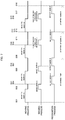
- FIG. 4 is a plan diagram illustrating the configuration of the printed circuit board and a moving sequence of an imaging visual field of a camera according to one or more embodiments;
- FIG. 5 is a flowchart showing part of a recognition mark extraction process according to one or more embodiments
- FIG. 6 is a flowchart showing part of the recognition mark extraction process according to one or more embodiments.
- FIG. 7 is a timing chart showing timings of various processing operations in the recognition mark extraction process according to one or more embodiments.
- FIG. 8 is a schematic configuration diagram schematically illustrating a solder printing inspection device according to one or more embodiments.
- FIG. 9 is a partially enlarged sectional view illustrating a lighting device for position detection according to one or more embodiments.
- FIG. 1 is a schematic configuration diagram schematically illustrating a solder printing inspection device 13 equipped with a substrate position detection device according one or more embodiments.
- the substrate position detection device according to one or more embodiments is embodied as one function of the solder printing inspection device 13 .
- a printed circuit board P 1 is configured such that a pattern (not shown) and lands 51 made of copper foil are formed on the surface of a flat plate-like base substrate 50 made of, for example, a glass epoxy resin. Portions of the surface of the base substrate 50 other than the lands 51 are coated with a resist film 52 . Solder paste 53 is printed on the lands 51 .
- Recognition marks are provided on the surface of the printed circuit board P 1 as objects of recognition for position detection. More specifically, a first recognition mark [A] and a second recognition mark [B] in a circular shape are respectively provided at two corners aligned on a predetermined diagonal line among four corners on the surface of the printed circuit board P 1 .
- the recognition marks [A] and [B] according to one or more embodiments are formed from copper foil, like the lands 51 .
- FIG. 2 is a block diagram illustrating the configuration of a production line 10 of the printed circuit board P 1 .
- the production line 10 is set such that the printed circuit board P 1 is conveyed rightward when being viewed from the front side.
- a solder printing machine 12 In the production line 10 , a solder printing machine 12 , the solder printing inspection device 13 , a component mounting machine 14 and a reflow device 15 are placed sequentially from its upstream side (left side in FIG. 2 ).
- the solder printing machine 12 is configured to print the solder paste 53 on the lands 51 of the printed circuit board P 1 .
- the solder printing inspection device 13 is configured to inspect the state of the solder paste 53 printed as described above. The details of the solder printing inspection device 13 will be described later.
- the component mounting machine 14 is configured to mount an electronic component such as a chip (not shown) on the printed solder paste 53 .
- the electronic component includes a plurality of electrodes and leads, and the respective electrodes and leads are temporarily mounted to predetermined locations of the solder paste 53 .
- the reflow device 15 is configured to heat and melt the solder paste 53 and solder joint (solder) the electrodes and the leads of the electronic component with the lands 51 .
- a conveyor 16 or the like configured to convey the printed circuit board P 1 is provided between the respective devices, for example, between the solder printing machine 12 and the solder printing inspection device 13 on the production line 10 (as shown in FIG. 2 ).
- a branching unit is provided between the solder printing inspection device 13 and the component mounting machine 14 , although not being illustrated.
- the printed circuit board P 1 determined as a non-defective by the solder printing inspection device 13 is guided to the component mounting machine 14 on the downstream side, whereas the printed circuit board P 1 determined as a defective is discharged to a defective storage by the branching unit.
- the solder printing inspection device 13 includes a conveyance mechanism 22 configured to, for example, convey and position the printed circuit board P 1 ; an inspection unit 23 configured to inspect the printed circuit board P 1 ; and a controller 26 configured to execute various controls, image processing and arithmetic processing in the solder printing inspection device 13 including drive control of the conveyance mechanism 22 and the inspection unit 23 (as shown in FIG. 3 ).
- the controller 26 is configured as the processing execution unit according to one or more embodiments.
- the conveyance mechanism 22 includes a pair of conveying rails 22 a placed along a conveying direction of the printed circuit board P 1 , an endless conveyor belt 22 b placed to be rotatable relative to the respective conveying rails 22 a , a drive unit (not shown) such as a motor configured to drive the conveyor belt 22 b , and a chuck mechanism (not shown) configured to position the printed circuit board P 1 at a predetermined position, and is driven and controlled by the controller 26 .
- a drive unit such as a motor configured to drive the conveyor belt 22 b
- a chuck mechanism (not shown) configured to position the printed circuit board P 1 at a predetermined position, and is driven and controlled by the controller 26 .
- the printed circuit board P 1 carried into the solder printing inspection device 13 is placed on the conveyor belt 22 b with respective edges of the printed circuit board P 1 in a width direction perpendicular to the conveying direction inserted into the respective conveying rails 22 a .
- the conveyor belt 22 b starts operation to convey the printed circuit board P 1 to a predetermined inspection position.
- the conveyor belt 22 b stops, and the chuck mechanism operates.
- the operation of the chuck mechanism presses up the conveyor belt 22 b , and the respective edges of the printed circuit board P 1 are held by the conveyor belt 22 b and the upper sides of the conveying rails 22 a .
- the printed circuit board P 1 is accordingly positioned and fixed at the inspection position.
- the configuration of the conveyance mechanism 22 is not limited to the configuration of one or more embodiments, but another configuration may be employed alternatively.
- the inspection unit 23 is placed above the conveying rails 22 a (conveyance path of the printed circuit board P 1 ).
- the inspection unit 23 includes a first illuminator 23 A and a second illuminator 23 B serving as the irradiator to irradiate a predetermined range (an inspection range or a recognition range) on the printed circuit board 1 obliquely downward with a predetermined light; a camera 23 C serving as the imaging unit (imager) to take an image of the predetermined range on the printed circuit board P 1 from immediately above; an X axis moving mechanism 23 D configured to allow for a move in an X-axis direction (shown in FIG. 3 ); and a Y axis moving mechanism 23 E configured to allow for a move in a Y-axis direction (shown in FIG. 3 ), and is driven and controlled by the controller 26 .
- Each of the first illuminator 23 A and the second illuminator 23 B is configured to change over the radiation light between light for three-dimensional measurement and light for position detection. More specifically, each of the first illuminator 23 A and the second illuminator 23 B is configured to irradiate a predetermined inspection range (inspection ranges “1” to “15” shown in FIG. 14 ) on the printed circuit board P 1 with a predetermined light for three-dimensional measurement (for example, patterned light having a striped light intensity distribution) and is also configured to irradiate a predetermined recognition range (the first recognition mark [A] or the second recognition mark [B] shown in FIG. 4 ) with a predetermined light for position detection (for example, uniform light having a fixed light intensity).
- a predetermined inspection range inspection ranges “1” to “15” shown in FIG. 14
- a predetermined light for three-dimensional measurement for example, patterned light having a striped light intensity distribution
- a predetermined recognition range
- the first illuminator 23 A includes a first light source 23 Aa configured to emit a predetermined light and a first liquid crystal shutter 23 Ab configured to transmit the light from the first light source 23 Aa, and is driven and controlled by the controller 26 .
- the first liquid crystal shutter 23 Ab is configured to form a first grating that converts the light from the first light source 23 Aa into a first patterned light having a striped light intensity distribution. Accordingly, the first illuminator 23 A changes over the radiation light between the uniform light and the pattered light by switching control of the first liquid crystal shutter 23 Ab.
- the second illuminator 23 B includes a second light source 23 Ba configured to emit a predetermined light and a second liquid crystal shutter 23 Bb configured to transmit the light from the second light source 23 Ba, and is driven and controlled by the controller 26 .
- the second liquid crystal shutter 23 Bb is configured to form a second grating that converts the light from the second light source 23 Ba into a second patterned light having a striped light intensity distribution. Accordingly, the second illuminator 23 B changes over the radiation light between the uniform light and the pattered light by switching control of the second liquid crystal shutter 23 Bb.
- Each of the first light source 23 Aa and the second light source 23 Ba is configured to change over the luminance of the radiation light in multiple stages.
- the light emitted from each of the light sources 23 Aa and 23 Ba is guided to a condenser lens (not shown) to be converted to parallel light, is guided to a projection lens (not shown) via the liquid crystal shutter 23 Ab or 23 Bb, and is projected as the uniform light or the patterned light on the printed circuit board P 1 .
- switching control of the liquid crystal shutter 23 Ab or 23 Bb is executed to shift the phase of each corresponding patterned light by every 1 ⁇ 4 pitch.
- the liquid crystal shutter 23 Ab or 23 Bb as the grating ensures radiation of the patterned light having a substantially ideal sinusoidal waveform. This configuration improves the measurement resolution of three-dimensional measurement.
- This configuration also provides electrical phase shift control of the patterned light and thereby achieves downsizing of the device.
- the inspection range or the recognition range on the printed circuit board P 1 is one area among a plurality of areas set in advance on the printed circuit board P 1 , in terms of the size of an imaging visual field (imaging range) K of the camera 23 C as one unit (as shown in FIG. 4 ).
- the controller 26 drives and controls the X axis moving mechanism 23 D and the Y axis moving mechanism 23 E to move the inspection unit 23 (imaging visual field K) to a location above an arbitrary inspection range or recognition range on the printed circuit board P 1 that is positioned and fixed at the inspection position.
- the inspection unit 23 is successively moved to a plurality of recognition ranges and inspection ranges set on the printed circuit board P 1 and executes a recognition process with regard to the respective recognition ranges and an inspection process with regard to the respective inspection ranges, so as to implement inspection of the entire area of the printed circuit board P 1 (as shown in FIG. 4 ).
- the X axis moving mechanism 23 D and the Y axis moving mechanism 23 E constitute the moving unit according to one or more embodiments.
- the camera 23 C is configured to include a lens, an imaging element and the like.
- a CCD sensor is employed as the imaging element.
- the imaging element is, however, not limited to the CCD sensor, and another imaging element such as a CMOS sensor may be employed alternatively.
- the camera 23 C is driven and controlled by the controller 26 . More specifically, the controller 26 executes an imaging process using the camera 23 C, in synchronism with an irradiation process using the illuminators 23 A and 23 B.
- Image data taken by the camera 23 C is converted into a digital signal inside of the camera 23 C, is transferred in the form of the digital signal to the controller 26 , and is stored in an image data storage device 34 described later.
- the controller 26 executes, for example, image processing and arithmetic processing, based on the image data, as described later.
- the controller 26 includes a CPU and input/output interfaces 31 (hereinafter referred to as “CPU and the like 31 ”) configured to control the entire solder printing inspection device 13 ; an input drive 32 serving as the “input unit” comprised of, for example, a keyboard, a mouse and a touch panel; a display device 33 serving as the “display unit” having a display screen such as a CRT or a liquid crystal display; an image data storage device 34 configured to store, for example, image data taken by the camera 23 C; a calculation result storage device 35 configured to store results of various calculations; and a set data storage device 36 configured to store in advance various information such as gerber data (including information with regard to recognition marks). These devices 32 to 36 are electrically connected with the CPU and the like 31 .
- CPU and the like 31 configured to control the entire solder printing inspection device 13 ; an input drive 32 serving as the “input unit” comprised of, for example, a keyboard, a mouse and a touch panel; a display device 33 serving as the “
- the set data storage device 36 stores information with regard to a plurality of recognition ranges and inspection ranges set on the printed circuit board P 1 and a moving sequence of the imaging visual field K of the camera 23 to these recognition ranges and inspection ranges.
- the “moving sequence of the imaging visual field K” specifies a sequence of moving the imaging visual field K of the camera 23 C with regard to the plurality of recognition ranges and inspection ranges set on the printed circuit board P 1 .
- the plurality of recognition ranges and the inspection ranges on the printed circuit board P 1 and the moving sequence of the imaging visual field K to these recognition ranges and inspection ranges may be set in advance automatically according to a predetermined program based on the gerber data and the like or may be set in advance manually by an operator.
- the imaging visual field K of the camera 23 C is first moved to a first recognition range corresponding to the first recognition mark [A] and is then moved to a second recognition range corresponding to the second recognition mark [B].
- the subsequent moving sequence of the imaging visual field K is set from a predetermined inspection range that is determined in advance as the starting point to take the shortest way as the moving route of the inspection unit 23 .
- the moving sequence (inspection sequence) of the imaging visual field K is set from an inspection range at an upper right corner as the starting point.
- each of ranges encircled by broken line frames represents the imaging visual field K (recognition range or inspection range), and the numerals “1” to “15” given to these ranges indicate the inspection sequence.
- the moving direction (moving route) of the imaging visual field K is shown by arrows.
- This inspection routine is executed by the controller 26 (CPU and the like 31 ).
- FIGS. 5 and 6 are flowcharts showing a recognition mark extraction process executed to detect the recognition marks [A] and [B].
- FIG. 7 is a timing chart showing timings of various processing operations in the recognition mark extraction process.
- the controller 26 first executes a moving process of moving the inspection unit 23 to adjust the imaging visual field K of the camera 23 C to the first recognition range corresponding to the first recognition mark [A] on the printed circuit board P 1 (step S 01 ).
- the controller 26 subsequently executes an imaging process of taking an image of the first recognition mark [A] on the printed circuit board P 1 with radiating uniform lights from the first illuminator 23 A and the second illuminator 23 B (step S 02 ).
- the controller 26 After termination of the imaging process of the first recognition mark [A], the controller 26 starts a moving process of moving the inspection unit 23 to a position corresponding to the second recognition mark [B] on the printed circuit board P 1 (step S 03 ), and simultaneously starts a recognition process of the first recognition mark [A], based on the image data of the first recognition mark [A] taken by this imaging process (step S 04 ).
- the first recognition mark [A] is recognized by detecting the edge of the first recognition mark [A], based on luminance values of the respective pixels included in the image data.
- the method of recognition of the first recognition mark [A] is, however, not limited to this technique, but another technique such as pattern matching may be employed (the same applies to the second recognition mark [B] described later).
- the controller 26 On termination of the recognition process of the first recognition mark [A], the controller 26 stores the result of the recognition in the calculation result storage device 35 . More specifically, the controller 26 stores an evaluation result of the image data that determines whether the first recognition mark [A] is recognizable from the image data obtained by the imaging process of step S 02 .
- the controller 26 when the first recognition mark [A] is successfully recognized by the above recognition process, the controller 26 subsequently calculates position information (for example, central coordinate) of the first recognition mark [A] and stores the position information of the first recognition mark [A] along with the evaluation result described above into the calculation result storage device 35 (the same applies to the second recognition mark [B] described later).
- the calculation process of the position information of the first recognition mark [A] may be executed along with a calculation process of position information (for example, central coordinate) of the second recognition mark [B] in the process of detecting position information of the printed circuit board P 1 after a successful recognition process of the second recognition mark [B] described later.
- the controller 26 executes an imaging process of taking an image of the second recognition mark [B] on the printed circuit board P 1 with radiating uniform lights from the first illuminator 23 A and the second illuminator 23 B (step S 05 ).
- the controller 26 determines whether the first recognition mark [A] is successfully recognized, based on the evaluation result of the image data with regard to the first recognition mark [A] stored in the calculation result storage device 35 (step S 06 ), and simultaneously starts a recognition process of the second recognition mark [B], based on the image data of the second recognition mark [B] obtained by the imaging process of step S 05 (step S 07 ).
- step S 06 When the determination process of step S 06 gives a determination result showing that the first recognition mark [A] is successfully recognized, the controller 26 waits for termination of the recognition process of the second recognition mark [B] of step S 07 and proceeds to a next process (step S 13 ).
- step S 07 On termination of the recognition process of the second recognition mark [B] of step S 07 , the controller 26 stores the result of the recognition in the calculation result storage device 35 as in the case of the first recognition mark [A] described above, and proceeds to the next process (step S 13 ).
- step S 06 When the determination process of step S 06 does not give the determination result showing that the first recognition mark [A] is successfully recognized, on the other hand, the controller 26 starts a retry process with regard to the first recognition mark [A]. More specifically, the controller 26 starts a moving process of moving the inspection unit 23 (the imaging visual field K of the camera 23 C) again to the position (first recognition range) corresponding to the first recognition mark [A] on the printed circuit board P 1 (step S 08 ). According to one or more embodiments (in the illustrated example of FIG. 7 ), the moving process (step S 08 ) is started after termination of the recognition process of the second recognition mark [B] (step S 07 ). This procedure is, however, not essential. According to a modification, the moving process (step S 08 ) may be started before termination of the recognition process of the second recognition mark [B] (step S 07 ).
- step S 09 After termination of the moving process of the inspection unit 23 to the position corresponding to the first recognition mark [A], the controller 26 executes a change process of imaging conditions with regard to the first recognition mark [A] (step S 09 ). According to a modification, the change process (step S 09 ) may be executed during the moving process of the inspection unit 23 .
- the controller 26 determines the excess or deficiency of the light intensity, based on the image data with regard to the first recognition mark [A] obtained by the previous imaging process and changes the light intensities of the uniform lights emitted from the first illuminator 23 A and the second illuminator 23 B. For example, when the image of the first recognition mark [A] taken as the image data is larger than the image stored as the gerber data, the controller 26 determines that the light intensity is excess and accordingly decreases the luminance values of the lights emitted from the first light source 23 Aa and the second light source 23 Ba.
- the controller 26 determines that the light intensity is deficient and accordingly increases the luminance values of the lights emitted from the first light source 23 Aa and the second light source 23 Ba.
- a modification may be configured to regulate the light intensities by controlling the liquid crystal shutters 23 Ab and 23 Bb.
- the controller 26 executes a re-imaging process of taking an image of the first recognition mark [A] on the printed circuit board P 1 again with radiating the uniform lights of the changed conditions from the first illuminator 23 A and the second illuminator 23 B (step S 10 ).
- the controller 26 executes a re-recognition process of the first recognition mark [A], based on the image data of the first recognition mark [A] obtained by the re-imaging process (step S 11 ).
- the re-recognition process of the first recognition mark [A] is similar to the recognition process (step S 04 ) described above and is not described in detail (the same applies to a re-recognition process of the second recognition mark [B] described later).
- the controller 26 subsequently determines whether the first recognition mark [A] is successfully recognized, based on the evaluation result of the image data with regard to the first recognition mark [A] (step S 12 ). When the determination process gives a determination result showing that the first recognition mark [A] is successfully recognized, the controller 26 proceeds to the next process (step S 13 ).
- step S 12 When the determination process of step S 12 does not give the determination result showing that the first recognition mark [A] is successfully recognized, on the other hand, the controller 26 returns to the change process of the imaging conditions of step S 09 described above and repeatedly executes the processing of step S 09 to step S 12 until the first recognition mark [A] is successfully recognized.
- the controller 26 determines whether the second recognition mark [B] is successfully recognized, based on the evaluation result of the image data with regard to the second recognition mark [B] stored in the calculation result storage device 35 (step S 13 ).
- step S 13 When the determination process of step S 13 gives a determination result showing that the second recognition mark [B] is successfully recognized, the controller 26 terminates the recognition mark extraction process.
- step S 13 When the determination process of step S 13 does not give the determination result showing that the second recognition mark [B] is successfully recognized, on the other hand, the controller 26 starts a retry process with regard to the second recognition mark [B]. More specifically, the controller 26 starts a moving process of moving the inspection unit 23 (the imaging visual field K of the camera 23 C) again to the position (second recognition range) corresponding to the second recognition mark [B] on the printed circuit board P 1 (step S 14 ).
- step S 08 to step S 12 When the retry process with regard to the first recognition mark [A] (processing of step S 08 to step S 12 ) is not executed, i.e., when appropriate image data with regard to the first recognition mark [A] is obtained by the first imaging process (step S 02 ), the imaging visual field K of the camera 23 C has already been adjusted to the second recognition range.
- the moving process of step S 14 is thus practically omitted.
- the moving process of step S 14 is executed as a confirmation process of checking whether the imaging visual field K of the camera 23 C positioned to the second recognition range.
- step S 15 After termination of the moving process (confirmation process) of the inspection unit 23 to the position corresponding to the second recognition mark [B], the controller 26 executes a change process of the imaging conditions with regard to the second recognition mark [B] (step S 15 ).
- the change process of the imaging conditions with regard to the second recognition mark [B] (step S 15 ) is similar to the change process of the imaging conditions with regard to the first recognition mark [A] (step S 09 ) and is thus not described in detail.
- the controller 26 executes a re-imaging process of taking an image of the second recognition mark [B] on the printed circuit board P 1 again with radiating the uniform lights of the changed conditions from the first illuminator 23 A and the second illuminator 23 B (step S 16 ).
- the controller 26 executes a re-recognition process of the second recognition mark [B], based on the image data of the second recognition mark [B] obtained by the re-imaging process (step S 17 ).
- the controller 26 subsequently determines whether the second recognition mark [B] is successfully recognized, based on the evaluation result of the image data with regard to the second recognition mark [B] (step S 18 ). When the determination process gives a determination result showing that the second recognition mark [B] is successfully recognized, the controller 26 terminates the recognition mark extraction process.
- step S 18 When the determination process of step S 18 does not give the determination result showing that the second recognition mark [B] is successfully recognized, on the other hand, the controller 26 returns to the change process of the imaging conditions of step S 15 described above and repeatedly executes the processing of step S 15 to step S 18 until the second recognition mark [B] is successfully recognized.
- the controller 26 calculates position information (for example, the inclination and the positional misalignment) of the printed circuit board P 1 , based on the position information (coordinates) of the first recognition mark [A] and the second recognition mark [B] detected by the recognition mark extraction process and position information (coordinates) of the first recognition mark [A] and the second recognition mark [B] stored as the gerber data.
- the controller 26 then terminates the position detection process of the printed circuit board P 1 .
- the controller 26 subsequently executes a correction process of correcting the misalignment of the relative positional relationship between the inspection unit 23 (camera 23 C) and the printed circuit board P 1 , based on the position information of the printed circuit board P 1 .
- the controller 26 subsequently starts a moving process of moving the inspection unit 23 to a position corresponding to the “first” inspection range on the printed circuit board P 1 according to the inspection sequence stored in the set data storage device 36 .
- the controller 26 executes an inspection process with regard to the “first” inspection range on the printed circuit board P 1 with radiating a striped pattern from the first illuminator 23 A or the second illuminator 23 B.
- This inspection process will be described later (the same applies to the inspection process with regard to any other inspection range).
- the controller 26 On termination of the inspection process with regard to the “first” inspection range on the printed circuit board P 1 , the controller 26 starts a moving process of moving the inspection unit 23 to a position corresponding to the “second” inspection range on the printed circuit board P 1 according to the inspection sequence stored in the set data storage device 36 .
- the controller 26 then similarly executes inspection processes with regard to the “second” to the “fifteenth” inspection ranges on the printed circuit board P 1 to terminate inspection with regard to the entire printed circuit board P 1 .
- This inspection process is executed by the controller 26 (the CPU and the like 31 ).
- the controller 26 executes four imaging processes under the first patterned light having different phases with changing the phase of the first patterned light radiated from the first illuminator 23 A and subsequently executes four imaging processes under the second patterned light having different phases with changing the phase of the second patterned light radiated from the second illuminator 23 B, so as to obtain a total of eight different image data. This series of processing is described in detail below.
- the controller 26 first drives and controls the X axis moving mechanism 23 D and the Y axis moving mechanism 23 E to move the inspection unit 23 and adjust the imaging visual field K of the camera 23 C to a predetermined inspection range on the printed circuit board P 1 , subsequently executes switching control of the liquid crystal shutters 23 Ab and 23 Bb of the two illuminators 23 A and 23 B, and sets the positions of the first grating and the second grating formed by the two liquid crystal shutters 23 Ab and 23 Bb to predetermined reference positions.
- the controller 26 On completion of changeover and setting of the first grating and the second grating, the controller 26 causes light emission from the first light source 23 Aa of the first illuminator 23 A to radiate the first pattered light and drives and controls the camera 23 C to execute a first imaging process under the first patterned light.
- the controller 26 turns off the first light source 23 Aa of the first illuminator 23 A and executes a switching process of the first liquid crystal shutter 23 Ab. More specifically, the controller 26 changes over and sets the position of the first grating formed by the first liquid crystal shutter 23 Ab from the reference position to a second position having the phase of the first patterned light shifted by 1 ⁇ 4 pitch (90 degrees).
- the controller 26 On completion of changeover and setting of the first grating, the controller 26 causes light emission from the light source 23 Aa of the first illuminator 23 A to radiate the first pattered light and drives and controls the camera 23 C to execute a second imaging process under the first patterned light.
- Four different image data under the first patterned light have the phases differing by 90 degrees each are obtained by repeatedly executing this series of processing.
- the controller 26 subsequently causes light emission from the second light source 23 Ba of the second illuminator 23 B to radiate the second pattered light and drives and controls the camera 23 C to execute a first imaging process under the second patterned light.
- the controller 26 turns off the second light source 23 Ba of the second illuminator 23 B and executes a switching process of the second liquid crystal shutter 23 Bb. More specifically, the controller 26 changes over and sets the position of the second grating formed by the second liquid crystal shutter 23 Bb from the reference position to a second position having the phase of the second patterned light shifted by 1 ⁇ 4 pitch (90 degrees).
- the controller 26 causes light emission from the light source 23 Ba of the second illuminator 23 B to radiate the second pattered light and drives and controls the camera 23 C to execute a second imaging process under the second patterned light.
- Four different image data under the second patterned light have the phases differing by 90 degrees each are obtained by repeatedly executing this series of processing.
- the controller 26 then executes three-dimensional measurement (height measurement) of the solder paste 53 by the known phase shift method, based on the four different image data taken under each of the patterned lights and stores the results of measurement into the calculation result storage device 35 .
- One or more embodiments execute three-dimensional measurement by radiating the patterned lights from two different directions. This configuration prevents the occurrence of any shade portion that is not irradiated with any patterned light.
- the controller 26 subsequently executes a quality judgment process of the solder paste 53 , based on the result of the three-dimensional measurement. More specifically, the controller 26 detects a printing range of the solder paste 53 that is higher than a reference plane, based on the measurement result of an inspection range obtained as described above, and integrates the heights at respective positions in the detected range to calculate the amount of the printed solder paste 53 .
- the controller 26 compares the data of the solder paste 53 regarding the position, the area, the height or the amount of the solder paste 53 thus obtained with reference data (for example, gerber data) stored in advance in the set data storage device 36 and determines whether the result of the comparison is in an allowable range, so as to determine the good/poor quality of the printing state of the solder paste 53 in the inspection range.
- reference data for example, gerber data
- the controller 26 While executing the good/poor quality determination described above after acquisition of the eight different image data as described above, the controller 26 moves the inspection unit 23 to a next inspection range.
- the above series of processing is repeatedly executed with regard to all the inspection ranges on the printed circuit board P 1 , so as to terminate inspection of the entire printed circuit board p 1 .
- the configuration of one or more embodiments executes the recognition process with regard to the first recognition mark [A] during the relative movement of the inspection unit 23 (the camera 23 C) to the position corresponding to the second recognition mark [B] after termination of the imaging process with regard to the first recognition mark [A].
- the configuration of one or more embodiments After termination of the imaging process with regard to the first recognition mark [A], the configuration of one or more embodiments starts the relative movement of the inspection unit 23 to the position corresponding to the second recognition mark [B] without waiting for the result of the recognition process, regardless of whether the first recognition mark [A] is successfully recognized.
- this configuration increases the speed of position detection of the printed circuit board P 1 when the first recognition mark [A] and the second recognition mark [B] are successfully recognized without the retry process (re-imaging process and re-recognition process).
- the configuration of one or more embodiments automatically executes the retry process (re-imaging process and re-recognition process).
- This configuration eliminates a need to stop the solder printing inspection device 13 (production line 10 ) and start the operator's manual operation. As a result, this configuration enhances the overall processing capacity and suppresses the productivity from being lowered.
- the configuration of one or more embodiments changes the imaging conditions in the case of executing the retry process. Accordingly, in the case of a failure in recognizing the first recognition mark [A] (or the second recognition mark [B]), the retry process is executed with automatically changing the imaging conditions (without the operator's manual operation). This configuration enables the first recognition mark [A] (or the second recognition mark [B]) of the failed recognition to be automatically recognized.
- the configuration of one or more embodiments determines the excess or deficiency of the light intensity, based on the image data with regard to the first recognition mark [A] (or the second recognition mark [B]) obtained by the previous imaging process and changes the light intensities of the uniform lights emitted from the first illuminator 23 A and the second illuminator 23 B. As a result, this enables the retry process to be executed under the more appropriate imaging conditions.
- FIG. 8 is a schematic configuration diagram schematically illustrating a solder printing inspection device 13 according to one or more embodiments.
- FIG. 9 is a partially enlarged sectional view illustrating a lighting device for position detection according to one or more embodiments.
- the first illuminator 23 A and the second illuminator 23 B are configured to change over the radiation light between the light for three-dimensional measurement and the light for position detection.
- One or more embodiments are, on the other hand, provided with an illuminator for radiating the light for position detection separately from the first illuminator 23 A and the second illuminator 23 B serving as the irradiator exclusive for three-dimensional measurement.
- an inspection unit 23 of one or more embodiments is configured to include an illumination device 71 for position detection, in addition to the first illuminator 23 A, the second illuminator 23 B and the camera 23 C.
- the illumination device 71 includes a first ring light 72 placed nearest to the printed circuit board P 1 , a second ring light 73 placed second nearest to the printed circuit board P 1 , and a third ring light 74 placed farthest from the printed circuit board P 1 .
- the respective ring lights 72 to 74 are configured to respectively change over and radiate monochromatic lights of three different colors, i.e., red light, green light and blue light.
- the first ring light 72 is configured to irradiate the printed circuit board P 1 with light at a large angle of incidence (for example, 74 degrees).
- the second ring light 73 is configured to irradiate the printed circuit board P 1 with light at a middle angle of incidence (for example, 20 degrees).
- the third ring light 74 is configured to irradiate the printed circuit board P 1 with light at a small angle of incidence (for example, 0 degree).
- the first imaging process with regard to the first recognition mark [A] (step S 02 ) and the first imaging process with regard to the second recognition mark [B] (step S 05 ) are executed under the monochromatic light emitted at the small angle of incidence from the third ring light 74 (“red light” according to one or more embodiments).
- the second ring light 73 is added in the change process of the imaging conditions (step S 09 and/or step S 15 ).
- a re-imaging process (step S 10 and/or step S 16 ) is then executed under two radiation lights, i.e., the monochromatic light emitted at the small angle of incidence from the third ring light 74 (“red light” according to one or more embodiments) and the monochromatic light emitted at the middle angle of incidence from the second ring light 73 (“red light” according to one or more embodiments).
- the monochromatic light emitted at the large angle of incidence from the first ring light 72 (“red light” according to one or more embodiments) is added in a second change process of the imaging conditions.
- a second re-imaging process is then executed under the monochromatic lights emitted from all the ring lights 72 to 74 (“red light” according to one or more embodiments).
- a third re-imaging process is executed under the monochromatic light emitted at the small angle of incidence from the third ring light 74 (“green light” according to one or more embodiments).
- a fourth re-imaging process is executed under two radiation lights, i.e., the monochromatic light emitted at the small angle of incidence from the third ring light 74 (“green light” according to one or more embodiments) and the monochromatic light emitted at the middle angle of incidence from the second ring light 73 (“green light” according to one or more embodiments).
- a fifth re-imaging process is executed under the monochromatic lights emitted from all the ring lights 72 to 74 (“green light” according to one or more embodiments).
- a sixth re-imaging process is executed under the monochromatic light emitted at the small angle of incidence from the third ring light 74 (“blue light” according to one or more embodiments).
- a seventh re-imaging process is executed under two radiation lights, i.e., the monochromatic light emitted at the small angle of incidence from the third ring light 74 (“blue light” according to one or more embodiments) and the monochromatic light emitted at the middle angle of incidence from the second ring light 73 (“blue light” according to one or more embodiments).
- an eighth re-imaging process is executed under the monochromatic lights emitted from all the ring lights 72 to 74 (“blue light” according to one or more embodiments).
- one or more embodiments have similar functions and advantageous effects to those of the embodiments described above.
- the configuration of one or more embodiments is especially effective when the surfaces of the recognition marks [A] and [B] are not flat as in the case of a solder leveler product.
- the embodiments described above are configured to determine the change process of the imaging conditions, based on the image data with regard to the first recognition mark [A] (or the second recognition mark [B]) obtained by the previous imaging process.
- One or more embodiments are, on the other hand, configured to change over and set the imaging conditions among the plurality of imaging conditions determined in advance in the predetermined sequence. This simplifies the change process of the imaging conditions.
- the present invention is not limited to the description of the above embodiments but may be implemented, for example, by configurations described below.
- the present invention may also be naturally implemented by applications and modifications other than those illustrated below.
- the substrate position detection device is embodied as one function of the solder printing inspection device 13 . This is, however, not essential.
- the substrate position detection device may be provided as part of another device, such as the solder printing machine 12 or the component mounting machine 14 , or may be provided independently.
- the substrate as the object of position detection by the substrate position detection device is not limited to the printed circuit board P 1 described in the above embodiments but may be, for example, a different type of printed circuit board, such as a double-sided substrate or a wafer substrate different from the printed circuit board.
- the printed circuit board P 1 is configured to have the first recognition mark [A] and the second recognition mark [B] in the circular shape at the two corners aligned on the predetermined diagonal line among the four corners, as the recognition objects for position detection.
- recognition marks may be provided at three or more positions on the printed circuit board P 1 .
- a through hole that is pierced from the surface to the rear face of the printed circuit board may be used as the recognition object for position detection.
- one or more embodiments are configured to change the light intensity, the radiation angle of the radiation light and the like by sequentially adding the ring lights 72 to 74 of the illumination device 71 one by one.
- a modification may be configured to change the radiation angle of the light or to change (the position of) the light source from which light is emitted by changing over the illumination (light source) one by one, for example, in the sequence of the “third ring light 74 ”, the “second ring light 73 ”, and the “first ring light 72 ”.
- Another modification may be configured to change the luminance values of the ring lights 72 to 74 of the illumination device 71 .
- the modification may be configured to change over the light source to the second ring light 73 (change the radiation angle).
- priority is given to the change of the radiation angle over the change of the light intensity in the change process of the imaging conditions.
- Another modification may be configured to change the imaging condition (light intensity) by changing the exposure time of the camera 23 C, the radiation time of the light or the like.
- the inspection sequence is set to take the shortest way as the moving route of the inspection unit 23 from a predetermined inspection range that is determined in advance (in the illustrated example of FIG. 4 , an inspection range at an upper right corner), as the starting point.
- the inspection sequence may be set to take the shortest way as the moving route of the inspection unit 23 from the second recognition mark [B] that is imaged last at the normal time (without any mark recognition error) between the first recognition mark [A] and the second recognition mark [B] as the starting point, or from an inspection range located nearest to the second recognition mark [B] as the starting point.
- the inspection sequence may be set to take the shortest way as the moving route of the inspection range 23 from the first recognition mark [A] or the second recognition mark [B] that is subject to the last retry process as the starting point, or from an inspection range located nearest to the first recognition mark [A] or the second recognition mark [B] as the starting point.
- the above configurations shorten the time period elapsed before a start of inspection with regard to the first inspection range and thereby increase the speed of the inspection.
Landscapes
- Engineering & Computer Science (AREA)
- Microelectronics & Electronic Packaging (AREA)
- Manufacturing & Machinery (AREA)
- Operations Research (AREA)
- Analytical Chemistry (AREA)
- Health & Medical Sciences (AREA)
- Life Sciences & Earth Sciences (AREA)
- Chemical & Material Sciences (AREA)
- Physics & Mathematics (AREA)
- Biochemistry (AREA)
- General Health & Medical Sciences (AREA)
- General Physics & Mathematics (AREA)
- Immunology (AREA)
- Pathology (AREA)
- Supply And Installment Of Electrical Components (AREA)
- Length Measuring Devices By Optical Means (AREA)
- Investigating Materials By The Use Of Optical Means Adapted For Particular Applications (AREA)
Applications Claiming Priority (3)
| Application Number | Priority Date | Filing Date | Title |
|---|---|---|---|
| JP2016-148230 | 2016-07-28 | ||
| JP2016148230A JP6276809B2 (ja) | 2016-07-28 | 2016-07-28 | 基板位置検出装置 |
| PCT/JP2017/015137 WO2018020752A1 (ja) | 2016-07-28 | 2017-04-13 | 基板位置検出装置 |
Related Parent Applications (1)
| Application Number | Title | Priority Date | Filing Date |
|---|---|---|---|
| PCT/JP2017/015137 Continuation WO2018020752A1 (ja) | 2016-07-28 | 2017-04-13 | 基板位置検出装置 |
Publications (2)
| Publication Number | Publication Date |
|---|---|
| US20190174662A1 US20190174662A1 (en) | 2019-06-06 |
| US10743448B2 true US10743448B2 (en) | 2020-08-11 |
Family
ID=61016986
Family Applications (1)
| Application Number | Title | Priority Date | Filing Date |
|---|---|---|---|
| US16/258,817 Active 2037-06-24 US10743448B2 (en) | 2016-07-28 | 2019-01-28 | Substrate position detection device |
Country Status (7)
| Country | Link |
|---|---|
| US (1) | US10743448B2 (ja) |
| JP (1) | JP6276809B2 (ja) |
| CN (1) | CN109315090B (ja) |
| DE (1) | DE112017003765T5 (ja) |
| MX (1) | MX2019000751A (ja) |
| TW (1) | TWI635786B (ja) |
| WO (1) | WO2018020752A1 (ja) |
Families Citing this family (4)
| Publication number | Priority date | Publication date | Assignee | Title |
|---|---|---|---|---|
| CN111492726B (zh) * | 2017-12-28 | 2021-09-03 | 株式会社富士 | 追踪装置 |
| WO2020016952A1 (ja) * | 2018-07-18 | 2020-01-23 | 株式会社Fuji | 部品認識装置および部品認識方法 |
| US20220252633A1 (en) * | 2019-07-22 | 2022-08-11 | The University Of Tokyo | Processing system, marking method, marker detected in said method, and marking program |
| EP4142436A4 (en) * | 2020-04-24 | 2023-05-17 | Fuji Corporation | CIRCUIT MANUFACTURING METHOD AND CIRCUIT MANUFACTURING DEVICE |
Citations (10)
| Publication number | Priority date | Publication date | Assignee | Title |
|---|---|---|---|---|
| JPH11261299A (ja) | 1998-03-16 | 1999-09-24 | Matsushita Electric Ind Co Ltd | 部品実装方法 |
| US7115435B2 (en) * | 2004-01-30 | 2006-10-03 | Ngk Spark Plug Co., Ltd. | Manufacturing method for wiring substrates |
| JP2008047905A (ja) | 2006-08-11 | 2008-02-28 | Samsung Electro Mech Co Ltd | 印刷回路基板の製造方法 |
| JP2009182280A (ja) | 2008-01-31 | 2009-08-13 | Hitachi High-Tech Instruments Co Ltd | 電子部品装着装置におけるマーク認識方法 |
| JP2010160006A (ja) | 2009-01-07 | 2010-07-22 | Hioki Ee Corp | 基板検査用カメラのための照明装置を備える基板検査装置 |
| US8335408B2 (en) * | 2007-11-20 | 2012-12-18 | Sony Corporation | Signal processing apparatus |
| US8389959B2 (en) * | 2009-01-30 | 2013-03-05 | Hitachi High-Technologies Corp. | Fluorescence analyzing device and fluorescence analyzing method |
| US8710783B2 (en) * | 2012-05-15 | 2014-04-29 | Panasonic Corporation | Motor control system, motor control device, and brushless motor |
| US8845114B2 (en) * | 2007-02-21 | 2014-09-30 | Panasonic Corporation | Lighting device for image capturing in electronic component mounting apparatus |
| US10564518B2 (en) * | 2014-11-24 | 2020-02-18 | John R. Tindall | Environmental lighting system and method |
Family Cites Families (1)
| Publication number | Priority date | Publication date | Assignee | Title |
|---|---|---|---|---|
| CN105473979B (zh) * | 2013-08-22 | 2018-09-28 | 富士机械制造株式会社 | 基板的生产作业方法、基板的拍摄条件决定方法及基板的生产作业装置 |
-
2016
- 2016-07-28 JP JP2016148230A patent/JP6276809B2/ja active Active
-
2017
- 2017-04-13 CN CN201780036475.8A patent/CN109315090B/zh active Active
- 2017-04-13 DE DE112017003765.4T patent/DE112017003765T5/de active Pending
- 2017-04-13 MX MX2019000751A patent/MX2019000751A/es active IP Right Grant
- 2017-04-13 WO PCT/JP2017/015137 patent/WO2018020752A1/ja active Application Filing
- 2017-04-24 TW TW106113562A patent/TWI635786B/zh active
-
2019
- 2019-01-28 US US16/258,817 patent/US10743448B2/en active Active
Patent Citations (10)
| Publication number | Priority date | Publication date | Assignee | Title |
|---|---|---|---|---|
| JPH11261299A (ja) | 1998-03-16 | 1999-09-24 | Matsushita Electric Ind Co Ltd | 部品実装方法 |
| US7115435B2 (en) * | 2004-01-30 | 2006-10-03 | Ngk Spark Plug Co., Ltd. | Manufacturing method for wiring substrates |
| JP2008047905A (ja) | 2006-08-11 | 2008-02-28 | Samsung Electro Mech Co Ltd | 印刷回路基板の製造方法 |
| US8845114B2 (en) * | 2007-02-21 | 2014-09-30 | Panasonic Corporation | Lighting device for image capturing in electronic component mounting apparatus |
| US8335408B2 (en) * | 2007-11-20 | 2012-12-18 | Sony Corporation | Signal processing apparatus |
| JP2009182280A (ja) | 2008-01-31 | 2009-08-13 | Hitachi High-Tech Instruments Co Ltd | 電子部品装着装置におけるマーク認識方法 |
| JP2010160006A (ja) | 2009-01-07 | 2010-07-22 | Hioki Ee Corp | 基板検査用カメラのための照明装置を備える基板検査装置 |
| US8389959B2 (en) * | 2009-01-30 | 2013-03-05 | Hitachi High-Technologies Corp. | Fluorescence analyzing device and fluorescence analyzing method |
| US8710783B2 (en) * | 2012-05-15 | 2014-04-29 | Panasonic Corporation | Motor control system, motor control device, and brushless motor |
| US10564518B2 (en) * | 2014-11-24 | 2020-02-18 | John R. Tindall | Environmental lighting system and method |
Non-Patent Citations (4)
| Title |
|---|
| International Preliminary Report on Patentability for corresponding International Application No. PCT/JP2017/015137, dated Feb. 7, 2019 (3 pages). |
| International Search Report for corresponding International Application No. PCT/JP2017/015137, dated Jul. 18, 2017 (5 pages). |
| Office Action in counterpart Japanese Patent Application No. 2016-148230 dated Sep. 5, 2017 (9 pages). |
| Written Opinion for corresponding International Application PCT/JP2017/015137, dated Jul. 18, 2017 (12 pages). |
Also Published As
| Publication number | Publication date |
|---|---|
| TWI635786B (zh) | 2018-09-11 |
| US20190174662A1 (en) | 2019-06-06 |
| JP2018018962A (ja) | 2018-02-01 |
| WO2018020752A1 (ja) | 2018-02-01 |
| DE112017003765T5 (de) | 2019-04-18 |
| JP6276809B2 (ja) | 2018-02-07 |
| TW201817305A (zh) | 2018-05-01 |
| CN109315090A (zh) | 2019-02-05 |
| CN109315090B (zh) | 2020-09-08 |
| MX2019000751A (es) | 2019-05-20 |
Similar Documents
| Publication | Publication Date | Title |
|---|---|---|
| US10743448B2 (en) | Substrate position detection device | |
| US10356298B2 (en) | Board inspection apparatus | |
| US10295479B2 (en) | Board inspection apparatus | |
| TWI622754B (zh) | Three-dimensional measuring device | |
| JP3872007B2 (ja) | 計測装置及び検査装置 | |
| EP3037776B1 (en) | Substrate production work method, substrate imaging condition determination method, and substrate production work device | |
| EP2685242B1 (en) | Vision testing device with enhanced image clarity | |
| US10679332B2 (en) | Solder printing inspection device | |
| JP2014508938A (ja) | 多重グリッドパターンを利用したビジョン検査装置 | |
| JP5989803B2 (ja) | 部品実装機及び部品実装方法 | |
| TW201721305A (zh) | 曝光裝置、曝光裝置之調正方法以及程式 | |
| WO2016174763A1 (ja) | 部品検査機及び部品装着機 | |
| JP6795520B2 (ja) | 実装装置および撮像処理方法 | |
| WO2012165261A1 (ja) | はんだマーク設定方法およびはんだマーク設定装置 | |
| JP2782759B2 (ja) | ハンダ付け外観検査装置 | |
| JP7365487B2 (ja) | 画像補正方法、撮像装置および検査装置 | |
| JP7000380B2 (ja) | 三次元計測装置及び三次元計測方法 | |
| JP6231397B2 (ja) | 部品認識装置、部品移載装置および部品実装装置 | |
| JP5946998B2 (ja) | 画像処理装置および電子部品実装機 | |
| JP7097504B2 (ja) | 対象体判定方法、対象体判定装置 | |
| JP2009206378A (ja) | 電子部品装着装置 | |
| WO2024111022A1 (ja) | 部品外観検査装置及び部品外観検査方法 | |
| KR101231188B1 (ko) | 부품실장기의 부품인식장치 및 이의 부품 위치보정방법 | |
| JP2008112931A (ja) | 電子部品装着装置 | |
| JPH0274849A (ja) | 基板検査のための検査領域設定方法およびその方法を用いた検査領域設定装置 |
Legal Events
| Date | Code | Title | Description |
|---|---|---|---|
| FEPP | Fee payment procedure |
Free format text: ENTITY STATUS SET TO UNDISCOUNTED (ORIGINAL EVENT CODE: BIG.); ENTITY STATUS OF PATENT OWNER: LARGE ENTITY |
|
| AS | Assignment |
Owner name: CKD CORPORATION, JAPAN Free format text: ASSIGNMENT OF ASSIGNORS INTEREST;ASSIGNORS:TAKAMURA, KENSUKE;UMEMURA, NOBUYUKI;REEL/FRAME:048520/0235 Effective date: 20190111 |
|
| STPP | Information on status: patent application and granting procedure in general |
Free format text: DOCKETED NEW CASE - READY FOR EXAMINATION |
|
| STPP | Information on status: patent application and granting procedure in general |
Free format text: NOTICE OF ALLOWANCE MAILED -- APPLICATION RECEIVED IN OFFICE OF PUBLICATIONS |
|
| STPP | Information on status: patent application and granting procedure in general |
Free format text: PUBLICATIONS -- ISSUE FEE PAYMENT VERIFIED |
|
| STCF | Information on status: patent grant |
Free format text: PATENTED CASE |
|
| MAFP | Maintenance fee payment |
Free format text: PAYMENT OF MAINTENANCE FEE, 4TH YEAR, LARGE ENTITY (ORIGINAL EVENT CODE: M1551); ENTITY STATUS OF PATENT OWNER: LARGE ENTITY Year of fee payment: 4 |