US10593901B2 - Processes for improving efficiency of light emitting diodes - Google Patents
Processes for improving efficiency of light emitting diodes Download PDFInfo
- Publication number
- US10593901B2 US10593901B2 US15/575,700 US201615575700A US10593901B2 US 10593901 B2 US10593901 B2 US 10593901B2 US 201615575700 A US201615575700 A US 201615575700A US 10593901 B2 US10593901 B2 US 10593901B2
- Authority
- US
- United States
- Prior art keywords
- led
- hydrogen
- period
- components
- exposing
- Prior art date
- Legal status (The legal status is an assumption and is not a legal conclusion. Google has not performed a legal analysis and makes no representation as to the accuracy of the status listed.)
- Expired - Fee Related
Links
- 238000000034 method Methods 0.000 title claims abstract description 46
- 230000008569 process Effects 0.000 title claims abstract description 17
- UFHFLCQGNIYNRP-UHFFFAOYSA-N Hydrogen Chemical compound [H][H] UFHFLCQGNIYNRP-UHFFFAOYSA-N 0.000 claims abstract description 130
- 229910052739 hydrogen Inorganic materials 0.000 claims abstract description 108
- 239000001257 hydrogen Substances 0.000 claims abstract description 108
- 239000002096 quantum dot Substances 0.000 claims description 57
- 150000002431 hydrogen Chemical class 0.000 claims description 17
- 239000007789 gas Substances 0.000 claims description 15
- 238000004519 manufacturing process Methods 0.000 claims description 12
- 238000002347 injection Methods 0.000 claims description 10
- 239000007924 injection Substances 0.000 claims description 10
- 229910052751 metal Inorganic materials 0.000 claims description 10
- 239000002184 metal Substances 0.000 claims description 10
- 239000002105 nanoparticle Substances 0.000 claims description 10
- 239000000203 mixture Substances 0.000 claims description 9
- 239000011521 glass Substances 0.000 claims description 7
- 230000005525 hole transport Effects 0.000 claims description 7
- 239000000758 substrate Substances 0.000 claims description 7
- 239000010410 layer Substances 0.000 description 39
- XLOMVQKBTHCTTD-UHFFFAOYSA-N Zinc monoxide Chemical compound [Zn]=O XLOMVQKBTHCTTD-UHFFFAOYSA-N 0.000 description 18
- XLYOFNOQVPJJNP-UHFFFAOYSA-N water Substances O XLYOFNOQVPJJNP-UHFFFAOYSA-N 0.000 description 14
- 239000000463 material Substances 0.000 description 13
- 239000004417 polycarbonate Substances 0.000 description 12
- 229920000515 polycarbonate Polymers 0.000 description 12
- 239000011787 zinc oxide Substances 0.000 description 9
- 229960001296 zinc oxide Drugs 0.000 description 8
- IJGRMHOSHXDMSA-UHFFFAOYSA-N Atomic nitrogen Chemical compound N#N IJGRMHOSHXDMSA-UHFFFAOYSA-N 0.000 description 7
- 239000002253 acid Substances 0.000 description 7
- 230000015572 biosynthetic process Effects 0.000 description 7
- 238000003786 synthesis reaction Methods 0.000 description 7
- 230000032683 aging Effects 0.000 description 6
- 230000007547 defect Effects 0.000 description 6
- 238000005538 encapsulation Methods 0.000 description 6
- CCCMONHAUSKTEQ-UHFFFAOYSA-N octadec-1-ene Chemical compound CCCCCCCCCCCCCCCCC=C CCCMONHAUSKTEQ-UHFFFAOYSA-N 0.000 description 6
- 230000000694 effects Effects 0.000 description 5
- XKRFYHLGVUSROY-UHFFFAOYSA-N Argon Chemical compound [Ar] XKRFYHLGVUSROY-UHFFFAOYSA-N 0.000 description 4
- 230000002378 acidificating effect Effects 0.000 description 4
- 229910052782 aluminium Inorganic materials 0.000 description 4
- XAGFODPZIPBFFR-UHFFFAOYSA-N aluminium Chemical compound [Al] XAGFODPZIPBFFR-UHFFFAOYSA-N 0.000 description 4
- -1 aromatic carboxylic acids Chemical class 0.000 description 4
- 230000008901 benefit Effects 0.000 description 4
- 239000011347 resin Substances 0.000 description 4
- 229920005989 resin Polymers 0.000 description 4
- QTBSBXVTEAMEQO-UHFFFAOYSA-N Acetic acid Chemical compound CC(O)=O QTBSBXVTEAMEQO-UHFFFAOYSA-N 0.000 description 3
- YXFVVABEGXRONW-UHFFFAOYSA-N Toluene Chemical compound CC1=CC=CC=C1 YXFVVABEGXRONW-UHFFFAOYSA-N 0.000 description 3
- 230000003679 aging effect Effects 0.000 description 3
- WPYMKLBDIGXBTP-UHFFFAOYSA-N benzoic acid Chemical compound OC(=O)C1=CC=CC=C1 WPYMKLBDIGXBTP-UHFFFAOYSA-N 0.000 description 3
- 238000006243 chemical reaction Methods 0.000 description 3
- 239000006059 cover glass Substances 0.000 description 3
- 238000000605 extraction Methods 0.000 description 3
- 229910052757 nitrogen Inorganic materials 0.000 description 3
- 230000003287 optical effect Effects 0.000 description 3
- 230000009467 reduction Effects 0.000 description 3
- 239000002904 solvent Substances 0.000 description 3
- RMZAYIKUYWXQPB-UHFFFAOYSA-N trioctylphosphane Chemical compound CCCCCCCCP(CCCCCCCC)CCCCCCCC RMZAYIKUYWXQPB-UHFFFAOYSA-N 0.000 description 3
- WRIDQFICGBMAFQ-UHFFFAOYSA-N (E)-8-Octadecenoic acid Natural products CCCCCCCCCC=CCCCCCCC(O)=O WRIDQFICGBMAFQ-UHFFFAOYSA-N 0.000 description 2
- LQJBNNIYVWPHFW-UHFFFAOYSA-N 20:1omega9c fatty acid Natural products CCCCCCCCCCC=CCCCCCCCC(O)=O LQJBNNIYVWPHFW-UHFFFAOYSA-N 0.000 description 2
- QSBYPNXLFMSGKH-UHFFFAOYSA-N 9-Heptadecensaeure Natural products CCCCCCCC=CCCCCCCCC(O)=O QSBYPNXLFMSGKH-UHFFFAOYSA-N 0.000 description 2
- LFQSCWFLJHTTHZ-UHFFFAOYSA-N Ethanol Chemical compound CCO LFQSCWFLJHTTHZ-UHFFFAOYSA-N 0.000 description 2
- BDAGIHXWWSANSR-UHFFFAOYSA-N Formic acid Chemical compound OC=O BDAGIHXWWSANSR-UHFFFAOYSA-N 0.000 description 2
- OFOBLEOULBTSOW-UHFFFAOYSA-N Malonic acid Chemical compound OC(=O)CC(O)=O OFOBLEOULBTSOW-UHFFFAOYSA-N 0.000 description 2
- 239000005642 Oleic acid Substances 0.000 description 2
- ZQPPMHVWECSIRJ-UHFFFAOYSA-N Oleic acid Natural products CCCCCCCCC=CCCCCCCCC(O)=O ZQPPMHVWECSIRJ-UHFFFAOYSA-N 0.000 description 2
- NINIDFKCEFEMDL-UHFFFAOYSA-N Sulfur Chemical compound [S] NINIDFKCEFEMDL-UHFFFAOYSA-N 0.000 description 2
- 238000013459 approach Methods 0.000 description 2
- 229910052786 argon Inorganic materials 0.000 description 2
- 229910001873 dinitrogen Inorganic materials 0.000 description 2
- DMBHHRLKUKUOEG-UHFFFAOYSA-N diphenylamine Chemical compound C=1C=CC=CC=1NC1=CC=CC=C1 DMBHHRLKUKUOEG-UHFFFAOYSA-N 0.000 description 2
- 239000002360 explosive Substances 0.000 description 2
- 239000000446 fuel Substances 0.000 description 2
- 238000004770 highest occupied molecular orbital Methods 0.000 description 2
- 125000004435 hydrogen atom Chemical group [H]* 0.000 description 2
- 230000006872 improvement Effects 0.000 description 2
- QXJSBBXBKPUZAA-UHFFFAOYSA-N isooleic acid Natural products CCCCCCCC=CCCCCCCCCC(O)=O QXJSBBXBKPUZAA-UHFFFAOYSA-N 0.000 description 2
- 238000004768 lowest unoccupied molecular orbital Methods 0.000 description 2
- QSHDDOUJBYECFT-UHFFFAOYSA-N mercury Chemical compound [Hg] QSHDDOUJBYECFT-UHFFFAOYSA-N 0.000 description 2
- 229910052753 mercury Inorganic materials 0.000 description 2
- 229910052987 metal hydride Inorganic materials 0.000 description 2
- 150000004681 metal hydrides Chemical class 0.000 description 2
- 150000007522 mineralic acids Chemical class 0.000 description 2
- ZQPPMHVWECSIRJ-KTKRTIGZSA-N oleic acid Chemical compound CCCCCCCC\C=C/CCCCCCCC(O)=O ZQPPMHVWECSIRJ-KTKRTIGZSA-N 0.000 description 2
- 238000011084 recovery Methods 0.000 description 2
- 239000011550 stock solution Substances 0.000 description 2
- KBIWNQVZKHSHTI-UHFFFAOYSA-N 4-n,4-n-dimethylbenzene-1,4-diamine;oxalic acid Chemical compound OC(=O)C(O)=O.CN(C)C1=CC=C(N)C=C1 KBIWNQVZKHSHTI-UHFFFAOYSA-N 0.000 description 1
- 239000005711 Benzoic acid Substances 0.000 description 1
- 229910004576 Cd1-xZnxS Inorganic materials 0.000 description 1
- YZCKVEUIGOORGS-OUBTZVSYSA-N Deuterium Chemical compound [2H] YZCKVEUIGOORGS-OUBTZVSYSA-N 0.000 description 1
- DGAQECJNVWCQMB-PUAWFVPOSA-M Ilexoside XXIX Chemical compound C[C@@H]1CC[C@@]2(CC[C@@]3(C(=CC[C@H]4[C@]3(CC[C@@H]5[C@@]4(CC[C@@H](C5(C)C)OS(=O)(=O)[O-])C)C)[C@@H]2[C@]1(C)O)C)C(=O)O[C@H]6[C@@H]([C@H]([C@@H]([C@H](O6)CO)O)O)O.[Na+] DGAQECJNVWCQMB-PUAWFVPOSA-M 0.000 description 1
- MUBZPKHOEPUJKR-UHFFFAOYSA-N Oxalic acid Natural products OC(=O)C(O)=O MUBZPKHOEPUJKR-UHFFFAOYSA-N 0.000 description 1
- 229920000144 PEDOT:PSS Polymers 0.000 description 1
- 229920001609 Poly(3,4-ethylenedioxythiophene) Polymers 0.000 description 1
- 239000004793 Polystyrene Substances 0.000 description 1
- ZLMJMSJWJFRBEC-UHFFFAOYSA-N Potassium Chemical compound [K] ZLMJMSJWJFRBEC-UHFFFAOYSA-N 0.000 description 1
- YZCKVEUIGOORGS-IGMARMGPSA-N Protium Chemical compound [1H] YZCKVEUIGOORGS-IGMARMGPSA-N 0.000 description 1
- 241000720974 Protium Species 0.000 description 1
- YZCKVEUIGOORGS-NJFSPNSNSA-N Tritium Chemical compound [3H] YZCKVEUIGOORGS-NJFSPNSNSA-N 0.000 description 1
- HCHKCACWOHOZIP-UHFFFAOYSA-N Zinc Chemical compound [Zn] HCHKCACWOHOZIP-UHFFFAOYSA-N 0.000 description 1
- 238000010521 absorption reaction Methods 0.000 description 1
- 235000011054 acetic acid Nutrition 0.000 description 1
- 229960000583 acetic acid Drugs 0.000 description 1
- ZOIORXHNWRGPMV-UHFFFAOYSA-N acetic acid;zinc Chemical compound [Zn].CC(O)=O.CC(O)=O ZOIORXHNWRGPMV-UHFFFAOYSA-N 0.000 description 1
- 150000007513 acids Chemical class 0.000 description 1
- 230000004913 activation Effects 0.000 description 1
- 239000000853 adhesive Substances 0.000 description 1
- 230000001070 adhesive effect Effects 0.000 description 1
- 125000001931 aliphatic group Chemical group 0.000 description 1
- 229910052783 alkali metal Inorganic materials 0.000 description 1
- 150000001340 alkali metals Chemical class 0.000 description 1
- 229910052784 alkaline earth metal Inorganic materials 0.000 description 1
- 150000001342 alkaline earth metals Chemical class 0.000 description 1
- 238000003491 array Methods 0.000 description 1
- JXLHNMVSKXFWAO-UHFFFAOYSA-N azane;7-fluoro-2,1,3-benzoxadiazole-4-sulfonic acid Chemical compound N.OS(=O)(=O)C1=CC=C(F)C2=NON=C12 JXLHNMVSKXFWAO-UHFFFAOYSA-N 0.000 description 1
- 235000010233 benzoic acid Nutrition 0.000 description 1
- UHYPYGJEEGLRJD-UHFFFAOYSA-N cadmium(2+);selenium(2-) Chemical compound [Se-2].[Cd+2] UHYPYGJEEGLRJD-UHFFFAOYSA-N 0.000 description 1
- 230000015556 catabolic process Effects 0.000 description 1
- GVPFVAHMJGGAJG-UHFFFAOYSA-L cobalt dichloride Chemical compound [Cl-].[Cl-].[Co+2] GVPFVAHMJGGAJG-UHFFFAOYSA-L 0.000 description 1
- 238000010276 construction Methods 0.000 description 1
- 230000007423 decrease Effects 0.000 description 1
- 230000003247 decreasing effect Effects 0.000 description 1
- 238000006731 degradation reaction Methods 0.000 description 1
- 239000002274 desiccant Substances 0.000 description 1
- 230000001627 detrimental effect Effects 0.000 description 1
- 229910052805 deuterium Inorganic materials 0.000 description 1
- 238000010494 dissociation reaction Methods 0.000 description 1
- 230000005593 dissociations Effects 0.000 description 1
- HCPOCMMGKBZWSJ-UHFFFAOYSA-N ethyl 3-hydrazinyl-3-oxopropanoate Chemical compound CCOC(=O)CC(=O)NN HCPOCMMGKBZWSJ-UHFFFAOYSA-N 0.000 description 1
- 238000002474 experimental method Methods 0.000 description 1
- 238000004880 explosion Methods 0.000 description 1
- 239000005357 flat glass Substances 0.000 description 1
- 235000019253 formic acid Nutrition 0.000 description 1
- 239000002803 fossil fuel Substances 0.000 description 1
- 229940093915 gynecological organic acid Drugs 0.000 description 1
- 238000005984 hydrogenation reaction Methods 0.000 description 1
- 238000011065 in-situ storage Methods 0.000 description 1
- 238000010348 incorporation Methods 0.000 description 1
- AMGQUBHHOARCQH-UHFFFAOYSA-N indium;oxotin Chemical compound [In].[Sn]=O AMGQUBHHOARCQH-UHFFFAOYSA-N 0.000 description 1
- 229910052500 inorganic mineral Inorganic materials 0.000 description 1
- 150000002739 metals Chemical class 0.000 description 1
- 239000011707 mineral Substances 0.000 description 1
- 238000012986 modification Methods 0.000 description 1
- 230000004048 modification Effects 0.000 description 1
- 239000002086 nanomaterial Substances 0.000 description 1
- QJGQUHMNIGDVPM-UHFFFAOYSA-N nitrogen(.) Chemical compound [N] QJGQUHMNIGDVPM-UHFFFAOYSA-N 0.000 description 1
- 229910052756 noble gas Inorganic materials 0.000 description 1
- 150000007524 organic acids Chemical class 0.000 description 1
- 235000005985 organic acids Nutrition 0.000 description 1
- 239000012044 organic layer Substances 0.000 description 1
- 229920002223 polystyrene Polymers 0.000 description 1
- 230000008092 positive effect Effects 0.000 description 1
- 229910052700 potassium Inorganic materials 0.000 description 1
- 239000011591 potassium Substances 0.000 description 1
- 239000002243 precursor Substances 0.000 description 1
- 230000002035 prolonged effect Effects 0.000 description 1
- 230000006798 recombination Effects 0.000 description 1
- 238000005215 recombination Methods 0.000 description 1
- 238000007788 roughening Methods 0.000 description 1
- 239000004065 semiconductor Substances 0.000 description 1
- 229910052708 sodium Inorganic materials 0.000 description 1
- 239000011734 sodium Substances 0.000 description 1
- 239000007787 solid Substances 0.000 description 1
- 239000000126 substance Substances 0.000 description 1
- 229910052722 tritium Inorganic materials 0.000 description 1
- 229910052725 zinc Inorganic materials 0.000 description 1
- 239000011701 zinc Substances 0.000 description 1
- 239000004246 zinc acetate Substances 0.000 description 1
Images


Classifications
-
- H—ELECTRICITY
- H10—SEMICONDUCTOR DEVICES; ELECTRIC SOLID-STATE DEVICES NOT OTHERWISE PROVIDED FOR
- H10K—ORGANIC ELECTRIC SOLID-STATE DEVICES
- H10K50/00—Organic light-emitting devices
- H10K50/10—OLEDs or polymer light-emitting diodes [PLED]
- H10K50/11—OLEDs or polymer light-emitting diodes [PLED] characterised by the electroluminescent [EL] layers
- H10K50/115—OLEDs or polymer light-emitting diodes [PLED] characterised by the electroluminescent [EL] layers comprising active inorganic nanostructures, e.g. luminescent quantum dots
-
- H01L51/502—
-
- F—MECHANICAL ENGINEERING; LIGHTING; HEATING; WEAPONS; BLASTING
- F21—LIGHTING
- F21V—FUNCTIONAL FEATURES OR DETAILS OF LIGHTING DEVICES OR SYSTEMS THEREOF; STRUCTURAL COMBINATIONS OF LIGHTING DEVICES WITH OTHER ARTICLES, NOT OTHERWISE PROVIDED FOR
- F21V7/00—Reflectors for light sources
- F21V7/22—Reflectors for light sources characterised by materials, surface treatments or coatings, e.g. dichroic reflectors
-
- H—ELECTRICITY
- H01—ELECTRIC ELEMENTS
- H01L—SEMICONDUCTOR DEVICES NOT COVERED BY CLASS H10
- H01L33/00—Semiconductor devices having potential barriers specially adapted for light emission; Processes or apparatus specially adapted for the manufacture or treatment thereof or of parts thereof; Details thereof
- H01L33/02—Semiconductor devices having potential barriers specially adapted for light emission; Processes or apparatus specially adapted for the manufacture or treatment thereof or of parts thereof; Details thereof characterised by the semiconductor bodies
- H01L33/04—Semiconductor devices having potential barriers specially adapted for light emission; Processes or apparatus specially adapted for the manufacture or treatment thereof or of parts thereof; Details thereof characterised by the semiconductor bodies with a quantum effect structure or superlattice, e.g. tunnel junction
- H01L33/06—Semiconductor devices having potential barriers specially adapted for light emission; Processes or apparatus specially adapted for the manufacture or treatment thereof or of parts thereof; Details thereof characterised by the semiconductor bodies with a quantum effect structure or superlattice, e.g. tunnel junction within the light emitting region, e.g. quantum confinement structure or tunnel barrier
-
- H—ELECTRICITY
- H01—ELECTRIC ELEMENTS
- H01L—SEMICONDUCTOR DEVICES NOT COVERED BY CLASS H10
- H01L33/00—Semiconductor devices having potential barriers specially adapted for light emission; Processes or apparatus specially adapted for the manufacture or treatment thereof or of parts thereof; Details thereof
- H01L33/02—Semiconductor devices having potential barriers specially adapted for light emission; Processes or apparatus specially adapted for the manufacture or treatment thereof or of parts thereof; Details thereof characterised by the semiconductor bodies
- H01L33/14—Semiconductor devices having potential barriers specially adapted for light emission; Processes or apparatus specially adapted for the manufacture or treatment thereof or of parts thereof; Details thereof characterised by the semiconductor bodies with a carrier transport control structure, e.g. highly-doped semiconductor layer or current-blocking structure
-
- H—ELECTRICITY
- H01—ELECTRIC ELEMENTS
- H01L—SEMICONDUCTOR DEVICES NOT COVERED BY CLASS H10
- H01L33/00—Semiconductor devices having potential barriers specially adapted for light emission; Processes or apparatus specially adapted for the manufacture or treatment thereof or of parts thereof; Details thereof
- H01L33/36—Semiconductor devices having potential barriers specially adapted for light emission; Processes or apparatus specially adapted for the manufacture or treatment thereof or of parts thereof; Details thereof characterised by the electrodes
-
- H—ELECTRICITY
- H01—ELECTRIC ELEMENTS
- H01L—SEMICONDUCTOR DEVICES NOT COVERED BY CLASS H10
- H01L33/00—Semiconductor devices having potential barriers specially adapted for light emission; Processes or apparatus specially adapted for the manufacture or treatment thereof or of parts thereof; Details thereof
- H01L33/48—Semiconductor devices having potential barriers specially adapted for light emission; Processes or apparatus specially adapted for the manufacture or treatment thereof or of parts thereof; Details thereof characterised by the semiconductor body packages
- H01L33/50—Wavelength conversion elements
- H01L33/501—Wavelength conversion elements characterised by the materials, e.g. binder
- H01L33/502—Wavelength conversion materials
- H01L33/504—Elements with two or more wavelength conversion materials
-
- H—ELECTRICITY
- H01—ELECTRIC ELEMENTS
- H01L—SEMICONDUCTOR DEVICES NOT COVERED BY CLASS H10
- H01L33/00—Semiconductor devices having potential barriers specially adapted for light emission; Processes or apparatus specially adapted for the manufacture or treatment thereof or of parts thereof; Details thereof
- H01L33/48—Semiconductor devices having potential barriers specially adapted for light emission; Processes or apparatus specially adapted for the manufacture or treatment thereof or of parts thereof; Details thereof characterised by the semiconductor body packages
- H01L33/50—Wavelength conversion elements
- H01L33/505—Wavelength conversion elements characterised by the shape, e.g. plate or foil
-
- H—ELECTRICITY
- H01—ELECTRIC ELEMENTS
- H01L—SEMICONDUCTOR DEVICES NOT COVERED BY CLASS H10
- H01L33/00—Semiconductor devices having potential barriers specially adapted for light emission; Processes or apparatus specially adapted for the manufacture or treatment thereof or of parts thereof; Details thereof
- H01L33/48—Semiconductor devices having potential barriers specially adapted for light emission; Processes or apparatus specially adapted for the manufacture or treatment thereof or of parts thereof; Details thereof characterised by the semiconductor body packages
- H01L33/58—Optical field-shaping elements
- H01L33/60—Reflective elements
-
- H—ELECTRICITY
- H10—SEMICONDUCTOR DEVICES; ELECTRIC SOLID-STATE DEVICES NOT OTHERWISE PROVIDED FOR
- H10K—ORGANIC ELECTRIC SOLID-STATE DEVICES
- H10K71/00—Manufacture or treatment specially adapted for the organic devices covered by this subclass
-
- H—ELECTRICITY
- H10—SEMICONDUCTOR DEVICES; ELECTRIC SOLID-STATE DEVICES NOT OTHERWISE PROVIDED FOR
- H10K—ORGANIC ELECTRIC SOLID-STATE DEVICES
- H10K71/00—Manufacture or treatment specially adapted for the organic devices covered by this subclass
- H10K71/40—Thermal treatment, e.g. annealing in the presence of a solvent vapour
Definitions
- the present invention relates in general to processes for making light emitting diodes (LED's) and in particular to fabrication processes to improve LED efficiency.
- LEDs Light emitting diodes
- LEDs are technologically and economically advantageous solid state light sources. LEDs are capable of reliably providing light with high brightness, hence in the past decades they have come to play a critical role in numerous applications, including flat-panel displays, traffic lights, and optical communications. When driven by a current, electrons and holes are injected into the junction region, where they recombine, releasing their energy by emitting photons. The efficiency of LEDs has important consequences on such applications. Conventional surface-emitting LEDs with high internal efficiencies suffer from relatively low external quantum efficiency. Quantum Dot LEDs, for example, exhibit external quantum efficiency of about 2-5%. These low external quantum efficiencies are independent of LED configuration, which may be bottom emitting, top emitting and/or inverted configuration.
- External quantum efficiency is the ratio of the number of photons emitted from an LED to the number of electrons injected into the LED. External quantum efficiency quantifies how efficiently an LED device coverts electrons to photons and allows them to escape in the form of visible light, or in some cases, infrared light. One way in which improved external quantum efficiency can be observed in by an increase of optical output by a positive aging effect.
- External quantum efficiency is a function of injection efficiency, internal quantum efficiency and extraction efficiency.
- Internal quantum efficiency is the proportion of all electron-hole recombination in the active region that produces photons
- extraction efficiency is the proportion of photons generated in the active region that escape from the device.
- Internal quantum efficiency and injection efficiency can be maximized by material selection for the appropriate bandgap, HOMO (highest occupied molecular orbital) and LUMO (lowest unoccupied molecular orbital) levels for organic layers, electron affinity, ionization potential, and work function for an inorganic layer during the construction of a device.
- Some methods have been used to increase external quantum efficiency such as using back mirrors, etched waveguides, reflective substrates or reflective intermediate layers within a LED, with limited success. Notwithstanding, to date no one has examined the effects of the fabrication process on an LED's external quantum efficiency.
- Quantum dot light emitting diodes QD-LEDs
- Inorganic quantum dot light emitters have a few advantages over organic light emitting diodes (OLEDs) and other light-emitting diodes, more important of which is excellent color purity.
- Quantum dots (QDs) are semiconductor nanocrystallites whose radii are smaller than the bulk exciton Bohr radius.
- Quantum confinement of electrons and holes in all three dimensions leads to an increase in the effective band gap of the QDs with decreasing crystallite size, where the optical absorption and emission of quantum dots shift to higher energies (blue shift) as the size of the dots decreases.
- a CdSe QD can emit light in any monochromatic visible color depending only on the size of the QD and can be used to form QD-LEDs arrays that emit white light.
- the emission color of quantum dot can also be tuned by its composition. For example, ZnxCd1-xS emits blue, ZnxCd1-xSySe1-y emits green, and ZnxCd1-xSe emits red.
- Suitable quantum dots are taught in US 2012/0138894 A1, which is incorporated herein in its entirety. It is appreciated that use of quantum dots improves devices external quantum efficiency. Nanoparticles are also known for improving the characteristics of devices. In particular, the incorporation of zinc oxide nanoparticles into LED devices further improves the efficiency and lifetime of LED devices
- a process for improving the external quantum efficiency of a light emitting diode is provided by exposing one or more components of an LED, a partially assembled LED, or a completely assembled LED to an amount of hydrogen or hydrogen gas, or to an atmosphere containing higher quantities of hydrogen or hydrogen gas for a period of exposure time.
- Kits and processes for constructing a light emitting diode having an improved external quantum efficiency are further provided, which includes exposing one or more components of an LED, a partially assembled LED, or a completely assembled LED to an amount of hydrogen or hydrogen gas, or to an atmosphere containing higher quantities of hydrogen or hydrogen gas for a period of exposure time.
- Exposing one or more components of an LED, a partially assembled LED, or a completely assembled LED to an amount of hydrogen or hydrogen gas, or to an atmosphere containing higher quantities of hydrogen or hydrogen gas for a period of exposure time has shown to improve the external quantum efficiency for a typical LED or QD-LED to near a 10 ⁇ improvement, showing external quantum efficiency upwards of 18% to 20%.
- FIG. 1 shows a schematic of the structure of a quantum dot (QD) LED with a nanoparticulate electron injection layer according to an embodiment of the invention.
- QD quantum dot
- FIG. 2 shows the reduced roll-off in efficiency after ZnO film exposure to hydrogen which is an indicator for improved charge balance.
- Good charge balance between electrons and holes is imperative for higher efficiencies and longer lifetimes in LEDs.
- FIG. 3 depicts the best efficiency achieved in a completed device after hydrogen exposure and water exposure.
- FIG. 4 illustrates a positive aging effect in addition to little-to-no non-uniformity in emission after exposing a completed LED device using degraded quantum dots.
- FIG. 5 illustrates external quantum efficiency data from a device exposed to hydrogen and then encapsulated with a non-acidic UV-cure resin.
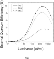
- FIG. 6 illustrates external quantum efficiency data from a device exposed to hydrogen and then encapsulated with a non-acidic UV-cure resin and baked for a period of time after encapsulation.
- FIGS. 7A and 7B illustrate spread in device performance.
- FIG. 7A depicts typical spread in device performance with typical encapsulation.
- FIG. 7B depicts spread in device performance with hydrogen treatment (encapsulated then baked).
- the present invention has utility as providing an LED with superior external quantum efficiency relative to conventional LEDs.
- the present invention achieves superior performance through exposing the components of the LEDs during fabrication, or though exposing a partially assembled or completely assembled LED. Notwithstanding, there still remains an unmet need to improve the external quantum efficiency of LEDs in the fabrication process of the components of the LED, such as the anode, the cathode, or quantum dots, to name a few. There further remains an unmet need to provide a method to assist in improving an aged LEDs.
- one or more components of an LED shall mean at least one glass cover, at least one quantum dot, at least one nanoparticle, at least one quantum dot layer, at least one nanoparticle layer, at least one cathode, at least one electron transport layer, at least one emission layer, at least one hole transport layer, at least one hole injection layer, at least one anode, at least one substrate, at least one intermediate layer, and at least one metal layer.
- positive aging effect shall mean the phenomenon where current efficiency, power efficiency and/or external quantum efficiency improve over time.
- an atmosphere containing higher quantities of hydrogen shall mean a defined space which contains an increased hydrogen concentration than normally found in air.
- an atmosphere containing higher quantities of hydrogen includes a glove box or polycarbonate chamber that contains some amount of hydrogen, whether the hydrogen is diatomic or monatomic hydrogen gas, and whether the hydrogen isotopes are deuterium, tritium, protium, or a combination thereof.
- the atmosphere containing higher quantities of hydrogen includes an N 2 H 2 gas mixture, with a H 2 concentration of 20% or higher.
- the hydrogen or hydrogen gas is an activated hydrogen or hydrogen gas. It is appreciated that atmosphere may be in a vacuum, atmospheric pressure, or pressurized.
- forming gas shall mean a mixture of hydrogen (mole fraction varies) and nitrogen gas.
- activated hydrogen shall mean a hydrogen molecule (H 2 ) where at least one of the electrons in the pair which binds the individual hydrogen atoms is excited, generating a pair of free hydrogen atoms that are energetically unfavorable and therefore quite reactive. Without being bound by any particular theory, hydrogen activation can occur where the bond in an H 2 molecule is cleaved by a photon of necessary energy (the bond dissociation energy of H 2 is 4.52 eV, which would require a photon wavelength of 274 nm). In some embodiments a mercury discharge lamp generating photons of 274 nm wavelength is used to generate an amount of activated hydrogen.
- polycarbonate chamber shall mean a sealable enclosure which may further include desiccants used for preserving moisture-sensitive items such as cobalt chloride paper for another use.
- desiccants used for preserving moisture-sensitive items such as cobalt chloride paper for another use.
- a common use for a polycarbonate chamber is to protect chemicals which are hygroscopic or which react with water from humidity.
- a “completely assembled LED” shall mean an LED containing at least at least one anode, at least one cathode, at least one p-type material, and at least one n-type material.
- a completely assembled LED includes at least one anode, at least one cathode, at least one electron transport layer, at least one hole transport layer and at least one emission layer.
- a completely assembled LED includes at least one substrate, at least one anode, at least one hole injection layer, at least one hole transport layer, at least one quantum dot emitting layer, at least one electron transport layer, at least one cathode, and at least one cover glass. It is appreciated that cover glass may be a flat glass or cavity glass depending on the encapsulation method.
- a “partially assembled LED” shall mean the connection or bonding of at least two of any of the components of an LED.
- a partially assembled LED includes at least one substrate, at least one anode, at least one hole injection layer, at least one hole transport layer, at least one quantum dot emitting layer, at least one electron transport layer, and at least one cathode, while not including at least one cover glass.
- a “degraded LED” or “degraded components” include any components of an LED, partially assembled LED, or completely assembled LED in which performance characteristics are below normal performance characteristics for the component, partially assembled devices, or completely assembled devices. In some embodiments an LED or component becomes degraded from extended use, or exposure to high currents or high ambient temperatures.
- range is intended to encompass not only the end point values of the range but also intermediate values of the range as explicitly being included within the range and varying by the last significant figure of the range.
- a recited range of from 1 to 4 is intended to include 1-2, 1-3, 2-4, 3-4, and 1-4.
- a method for improving the efficiency of a light emitting diode includes exposing one or more components of an LED, a partially assembled LED, or a completely assembled LED to an amount of hydrogen or hydrogen gas.
- Alternative embodiments of the invention include exposing one or more components of an LED, a partially assembled LED, or a completely assembled LED to an atmosphere containing higher quantities of hydrogen or hydrogen gas.
- the exposing of the one or more components of an LED, a partially assembled LED, or a completely assembled LED for a period of exposure time. Without being bound to any particular theory, it is believed that by exposing LED components or exposing partially or completely assembled LEDs to hydrogen, causes a bonding of hydrogen to the defect state and reduction of the negative effects of these states.
- LED components include at least one glass cover, at least one quantum dot, at least one nanoparticle, at least one quantum dot layer, at least one nanoparticle layer, at least one cathode, at least one electron transport layer, at least one emission layer, at least one hole transport layer, at least one hole injection layer, at least one anode, at least one substrate, at least one intermediate layer, and at least one metal layer.
- an emission layer includes at least one quantum dot.
- Hydrogen sources include gas canisters or tanks, gas candles, and forming gas. Additional hydrogen sources include solvents, adhesives, organic acids, fossil fuels, and fuel cells (metal hydride for example). Some hydrogen sources may be directly applied, while other hydrogen sources are placed in the vicinity of the fabrication or encapsulation methods and the hydrogen gasses from the solvent or other hydrogen source. It should be appreciated that hydrogen concentrations should be limited as a result of the combustibility of hydrogen. To reduce the risk of explosion, hydrogen concentrations of less than 18% are recommended. Notwithstanding, in at least one embodiment the materials, components, partially assembled, or completely assembled LEDs are exposed to a hydrogen concentration is 20% or less. Hydrogen is normally mixed with one or more gases in order to maintain the concentrations below explosive levels.
- the hydrogen atmosphere is a mixture of hydrogen gas and at least one other gas, a mixture of hydrogen gas and nitrogen gas, a mixture of a hydrogen gas and a noble gas, or combinations thereof.
- Exposure time of the materials, components, partially assembled LEDs, or completely assembled LEDs may vary based on preference, but it has been found that longer hydrogen exposure times have a greater effect on improving the efficiency of devices.
- the period of exposure time is at least thirty minutes, is at least twelve hours, or is at least twenty four hours. It is appreciated that exposure times may be increased for any duration of time and that certain materials or components would benefit from such exposure thus further improving the efficiency and potentially increasing the lifetime of a particular device.
- Hydrogen exposure may occur in the presence of an argon or forming gas environment.
- the materials, components, partially assembled LEDs, or completely assembled LED are baked for a period of baking time. Similar to the hydrogen exposure different bake times have provided improved results. In at least one embodiment the period of baking time is at least thirty minutes, at least twelve hours, or at least twenty four hours.
- the baking of the materials, components, partially assembled LEDs, or completely assembled LEDs have been tested at various temperatures, but bake temperatures should be limited especially since the explosive nature of hydrogen. In at least one embodiment the materials, components, partially assembled LEDs, or completely assembled LED baking occurs at a temperature less than 150° C.
- Some embodiments further include exposing the materials, components, partially assembled LEDs, or completely assembled LEDs to an amount of water, thus further improving the performance and efficiencies of an LED.
- one or more components of an LED, partially assembled LEDs, or completely assembled LEDs are exposed to an amount of water while exposing to an amount of hydrogen or hydrogen gas, or to an atmosphere containing higher quantities of hydrogen or hydrogen gas. It is appreciated that the water and hydrogen exposure can also be combined with baking, thus including all inventive processes disclosed herein.
- one or more components of LEDs, partially assembled LEDs, or completely assembled LEDs are exposed to an amount of water, to baking, to an amount of hydrogen or hydrogen gas, or to an atmosphere containing higher quantities of hydrogen or hydrogen gas.
- one or more quantum dots after synthesis, is exposed to activated hydrogen generated by reactive metal and weak acid.
- one or more quantum dots are purified in hydrogen environment.
- the components of an LED are fabricated in a hydrogen environment.
- quantum dots were synthesized in a hydrogen atmosphere.
- quantum dot after synthesis is exposed to activated hydrogen generated by reactive metal and weak acid. “In at least one embodiment, quantum dot after synthesis is exposed to hydrogen generated by placing the one or more quantum dots in the presence of a solvent or other hydrogen source.
- zinc oxide nanoparticles were synthesized in a hydrogen atmosphere.
- the LEDs are assembled or partially assembled in a hydrogen environment.
- in-situ hydrogenation of quantum dots can be done by generating hydrogen in the reactor after quantum dot synthesis.
- Hydrogen can be generated using reactive metal and weak acids [Note: strong acid (mineral/inorganic acids) reacts/dissolves/corrodes QDs]. Any metals which are electropositive than hydrogen can be used as a metal source; these metal sources include alkali metals, alkaline earth metals, zinc, aluminum etc. Aliphatic or aromatic carboxylic acids and alcohol and can be used as acid source.
- Aliphatic mono-carboxylic acid such as methanoic acid, ethanoic acid; dicarboxylic acid such as ethanedioic acid, propanedioic acid; aromatic carboxylic acid such as benzoic acid and their derivatives can be used as an acid.
- Alcohol can be used as an acid when very reactive metal like sodium or potassium are used for hydrogen generation.
- LEDs have lower performance characteristics as a result to fluctuations or inconsistencies in the fabrication process of the LED components.
- LEDs degrade over time as a result of prolonged use. Additional factors which may cause degradation of an LED include the amount of electrical current through the LED, i 2 R losses, or the ambient temperature which an LED is used.
- Recovery is achieved by exposure of a degraded LED, partially assembled degraded LED, or a completely assembled degraded LED to an amount of hydrogen, hydrogen gas or activated hydrogen, or to an atmosphere containing higher quantities of hydrogen, hydrogen gas or activated hydrogen, wherein said exposing occurs for a period of component exposure time.
- baking, or exposure to a water source is similarly used.
- the methods and kits described herein may be used for any type of LED or degraded LED.
- the LED or degraded LED is a quantum dot LED (QD LED).
- the LED or degraded LED is an organic LED (OLED). While in other embodiments, the LED or degraded LED is an inorganic LED.
- the following quantum dot synthesis was performed in a glove box containing 18% hydrogen and 82% nitrogen gases.
- 0.2 mmol of CdO, 4 mmol of zinc acetate and 5 ml of oleic acid (OA) were placed in a 50 ml flask and heated to 170° C. in flowing high-purity argon for 30 min.
- 15 ml of 1-octadecene (ODE) was added to the flask and the temperature was elevated to 300° C.
- a stock solution containing 0.1 mmol of Se and 3.5 mmol of S dissolved in 2 ml of trioctylphosphine (TOP) was quickly injected into the flask.
- the reaction temperature was kept for 10 min and then cooled to room temperature.
- the resulting quantum dots (QDs) were washed several times and finally dispersed in toluene.
- the relative ratios of the precursors were varied in order to form QDs with different emissions and nanostructures.
- the procedure is the same as described above, except that the stock solutions were injected twice.
- the sulfur powder dissolved in ODE was quickly injected into the flask and the temperature was increased to 310° C.
- sulfur powder dissolved in TOP was then introduced into the reactor for ZnS shell growth of 40 min at 310° C., and then cooled to room temperature.
- a quantum dot LED was assembled in an environment having elevated hydrogen concentrations.
- the QD-LED is shown schematically in FIG. 1 , and consists of an indium-tin oxide (ITO) transparent anode on a glass substrate, a poly(3,4-ethylenedioxythiophene):polystyrene sulphonate (PEDOT:PSS)hole injection layer, a poly(9,9-dioctylfluorene-co-N-(4-(3-methylpropyl))diphenylamine) (TFB) hole transport layer, quantum dots as the emissive layer, an electron transport layer of ZnO nanoparticles and an aluminum (Al) cathode.
- ITO indium-tin oxide
- PEDOT:PSS poly(3,4-ethylenedioxythiophene):polystyrene sulphonate
- TFB poly(9,9-dioctylfluorene-co-N-(
- An LED including an electron transport layer of a zinc-oxide (ZnO) film was assembled in a high purity nitrogen glove box environment, other than the ZnO film being exposed to a hydrogen environment for at least 12 hours.
- the procedure for exposing the ZnO film to hydrogen involves some additional steps beyond typical LED assembly.
- the QD-LED is assembled up through the ZnO NPs layer.
- FIG. 1 depicts the layers included, but the aluminum cathode is not yet deposited.
- the unfinished device is placed in a polycarbonate chamber and then sealed such that the atmosphere in the chamber is the same as in the glove box. Then, the polycarbonate chamber is removed from the glove box and evacuated to a pressure of ⁇ 10 mbar for 5 minutes.
- the polycarbonate chamber is then back-filled with a mixture of nitrogen and hydrogen gas for a given period of time. Finally, the polycarbonate chamber is brought back inside the glove box and the aluminum cathode is deposited.
- the external quantum efficiency as a function of current density is shown in FIG. 2 as compared to an identical device not assembled in an elevated hydrogen environment.
- the QD-LED of Example 2 was assembled in a high-purity glove box environment. Upon the completion of the LED assembly, the LED was exposed to a forming gas containing 20% hydrogen within a polycarbonate chamber for a period greater than 24 hours. A surprising result was observed of increased external quantum efficiency, increased luminance and lifetime, thus showing positive aging affects with hydrogen treatment. Similar results were observed by exposing partially assembled LEDs to a similar environment.
- the QD-LED of Example 2 was assembled in a high-purity glove box environment. Prior to the completion of the LED assembly, the LED was exposed to a forming gas containing 20% hydrogen within a polycarbonate chamber for a period greater than 24 hours device then encapsulated with a non-acidic UV-cure resin.
- the external quantum efficiency as a function of luminance for the assembled LED is shown over a five day period after assembly in FIG. 5 .
- a surprising result was observed of increased external quantum efficiency, increased luminance and time, thus showing positive aging affects with hydrogen treatment. No water was intentionally introduced into the atmosphere during exposure and the hydrogen was not activated.
- Example 5 was repeated with the additional step of baking the LED for a period of time after encapsulation with a non-acidic UV-cure resin.
- the external quantum efficiency as a function of luminance for the assembled LED is shown over a five day period after assembly in FIG. 6 .
- FIG. 7A depicts typical spread in device performance with typical encapsulation.
- FIG. 7B depicts spread in device performance with hydrogen treatment (encapsulated then baked).
- a surprising result was observed with the additional baking step accelerating the positive aging to a moderate extent in comparing FIG. 7 to FIG. 6 .
- the QD-LED of Example 2 was assembled in a high-purity glove box environment. Upon the completion of the LED assembly, the LED was exposed to a forming gas containing 20% hydrogen within a polycarbonate chamber for a period greater than 24 hours. During this same period, a small vial of water was additionally present in the polycarbonate chamber.
- the external quantum efficiency as a function of luminance for the assembled LED is shown in FIG. 3 , as compared to an identical device not exposed to a hydrogen and water environment.
- a surprising result was observed with improved changes in efficiency over time, thus showing positive aging affects with hydrogen and water treatment. Similar results were observed by exposing partially assembled LEDs to a similar environment. Other experiments were performed varying the amount of water used. Detrimental effects were observed for higher concentrations of water being used.
- the QD-LED of Example 2 was assembled in a high-purity glove box environment using degraded quantum dots. Upon the completion of the LED assembly, the LED was exposed to a forming gas containing 20% hydrogen within a polycarbonate chamber with a mercury discharge lamp emitting light with a 254 nm wavelength generating an amount of activated hydrogen within the environment. The lamp was left on for 4 hours but the QD-LEDs remained in the chamber for an additional 12 hours.
- the external quantum efficiency as a function of luminance for the assembled LED is shown in FIG. 4 as compared to an identical device not exposed to an activated hydrogen environment. A surprising result was observed with improved changes in efficiency, thus showing positive effects with the activated hydrogen treatment. Similar results were observed by exposing partially assembled LEDs to a similar environment.
- the QD-LED of Example 2 is assembled in a high-purity glove box environment. Upon the completion of the LED assembly, the LED was encapsulated with a cavity glass in a hydrogen environment to create a standing Hydrogen environment. A surprising result was observed of a maintained increased external quantum efficiency, increased luminance and lifetime, thus showing positive aging affects with hydrogen treatment.
- the QD-LED of Example 2 is assembled in a high-purity glove box environment. Upon the completion of the LED assembly, the LED is encapsulated with a cavity glass in a hydrogen environment containing a metal hydride fuel cell for continued Hydrogen production and exposure. A surprising result was observed of a maintained increased external quantum efficiency, increased luminance and lifetime, thus showing positive aging affects with hydrogen treatment.
- Patent documents and publications mentioned in the specification are indicative of the levels of those skilled in the art to which the invention pertains. These documents and publications are incorporated herein by reference to the same extent as if each individual document or publication was specifically and individually incorporated herein by reference.
Landscapes
- Engineering & Computer Science (AREA)
- Microelectronics & Electronic Packaging (AREA)
- Manufacturing & Machinery (AREA)
- Computer Hardware Design (AREA)
- Power Engineering (AREA)
- Inorganic Chemistry (AREA)
- Chemical & Material Sciences (AREA)
- Crystallography & Structural Chemistry (AREA)
- Nanotechnology (AREA)
- Physics & Mathematics (AREA)
- Optics & Photonics (AREA)
- General Engineering & Computer Science (AREA)
- Led Device Packages (AREA)
- Electroluminescent Light Sources (AREA)
- Luminescent Compositions (AREA)
- Led Devices (AREA)
Priority Applications (1)
| Application Number | Priority Date | Filing Date | Title |
|---|---|---|---|
| US15/575,700 US10593901B2 (en) | 2015-05-20 | 2016-05-20 | Processes for improving efficiency of light emitting diodes |
Applications Claiming Priority (3)
| Application Number | Priority Date | Filing Date | Title |
|---|---|---|---|
| US201562164104P | 2015-05-20 | 2015-05-20 | |
| PCT/US2016/033405 WO2016187492A1 (en) | 2015-05-20 | 2016-05-20 | Processes for improving efficiency of light emitting diodes |
| US15/575,700 US10593901B2 (en) | 2015-05-20 | 2016-05-20 | Processes for improving efficiency of light emitting diodes |
Publications (2)
| Publication Number | Publication Date |
|---|---|
| US20180212177A1 US20180212177A1 (en) | 2018-07-26 |
| US10593901B2 true US10593901B2 (en) | 2020-03-17 |
Family
ID=57320898
Family Applications (1)
| Application Number | Title | Priority Date | Filing Date |
|---|---|---|---|
| US15/575,700 Expired - Fee Related US10593901B2 (en) | 2015-05-20 | 2016-05-20 | Processes for improving efficiency of light emitting diodes |
Country Status (7)
| Country | Link |
|---|---|
| US (1) | US10593901B2 (zh) |
| EP (1) | EP3286779A4 (zh) |
| JP (1) | JP2018517247A (zh) |
| KR (1) | KR20180013980A (zh) |
| CN (1) | CN107710387A (zh) |
| TW (1) | TWI737610B (zh) |
| WO (1) | WO2016187492A1 (zh) |
Cited By (1)
| Publication number | Priority date | Publication date | Assignee | Title |
|---|---|---|---|---|
| US11770942B2 (en) | 2020-04-28 | 2023-09-26 | Samsung Display Co., Ltd. | Display apparatus |
Families Citing this family (3)
| Publication number | Priority date | Publication date | Assignee | Title |
|---|---|---|---|---|
| CN107104194B (zh) * | 2017-05-26 | 2019-07-12 | 吉林大学 | 一种双面发光的无机钙钛矿量子点led及其制备方法 |
| US10418578B2 (en) * | 2017-09-22 | 2019-09-17 | Shenzhen China Star Optoelectronics Semiconductor Display Technology Co., Ltd. | Quantum dot light-emitting diode and display device |
| CN110165063A (zh) * | 2019-05-27 | 2019-08-23 | 深圳市华星光电技术有限公司 | 量子棒发光二极管器件 |
Citations (10)
| Publication number | Priority date | Publication date | Assignee | Title |
|---|---|---|---|---|
| US5030536A (en) | 1989-12-26 | 1991-07-09 | Xerox Corporation | Processes for restoring amorphous silicon imaging members |
| US5923946A (en) | 1997-04-17 | 1999-07-13 | Cree Research, Inc. | Recovery of surface-ready silicon carbide substrates |
| US5932896A (en) * | 1996-09-06 | 1999-08-03 | Kabushiki Kaisha Toshiba | Nitride system semiconductor device with oxygen |
| US20040109483A1 (en) | 2002-12-10 | 2004-06-10 | Simpson John T. | Nanocrystal waveguide (NOW) laser |
| EP1516944A1 (en) | 2003-09-09 | 2005-03-23 | Samsung Electronics Co., Ltd | The improvement of the luminescent efficiency of Semiconductor Nanocrystals by Surface Treatment |
| US20060071218A1 (en) * | 2002-12-16 | 2006-04-06 | Japan Science And Technology Agency | Semiconductior multilayer structurehaving inhomogeneous quantum dots, light-emitting diode using same, semiconductor laser diode, semiconductor optical amplifier, and method for manufacturing them |
| US20080283388A1 (en) * | 2007-05-15 | 2008-11-20 | Japan Atomic Energy Agency | Hydrogen gas detecting membrane |
| US20100007267A1 (en) | 2008-07-09 | 2010-01-14 | Ushiodenki Kabushiki Kaisha | Light emitting device and method for producing the light emitting device |
| WO2011005859A2 (en) | 2009-07-07 | 2011-01-13 | University Of Florida Research Foundation, Inc. | Stable and all solution processable quantum dot light-emitting diodes |
| EP2803714A1 (en) | 2013-05-15 | 2014-11-19 | Kabushiki Kaisha Toshiba | SiAlON:Ce phosphor |
Family Cites Families (3)
| Publication number | Priority date | Publication date | Assignee | Title |
|---|---|---|---|---|
| JP4046512B2 (ja) * | 2002-01-25 | 2008-02-13 | 株式会社半導体エネルギー研究所 | 発光装置の作製方法 |
| KR100870837B1 (ko) * | 2008-03-04 | 2008-11-28 | 한국철강 주식회사 | 산화아연 박막의 수분 제거 방법 |
| KR20160035581A (ko) * | 2013-07-19 | 2016-03-31 | 에이제트 일렉트로닉 머티어리얼스 (룩셈부르크) 에스.에이.알.엘. | 발광다이오드를 위한 봉지재 |
-
2016
- 2016-05-19 TW TW105115606A patent/TWI737610B/zh active
- 2016-05-20 JP JP2017560791A patent/JP2018517247A/ja active Pending
- 2016-05-20 CN CN201680028079.6A patent/CN107710387A/zh active Pending
- 2016-05-20 WO PCT/US2016/033405 patent/WO2016187492A1/en active Application Filing
- 2016-05-20 EP EP16797349.4A patent/EP3286779A4/en not_active Withdrawn
- 2016-05-20 KR KR1020177036634A patent/KR20180013980A/ko unknown
- 2016-05-20 US US15/575,700 patent/US10593901B2/en not_active Expired - Fee Related
Patent Citations (10)
| Publication number | Priority date | Publication date | Assignee | Title |
|---|---|---|---|---|
| US5030536A (en) | 1989-12-26 | 1991-07-09 | Xerox Corporation | Processes for restoring amorphous silicon imaging members |
| US5932896A (en) * | 1996-09-06 | 1999-08-03 | Kabushiki Kaisha Toshiba | Nitride system semiconductor device with oxygen |
| US5923946A (en) | 1997-04-17 | 1999-07-13 | Cree Research, Inc. | Recovery of surface-ready silicon carbide substrates |
| US20040109483A1 (en) | 2002-12-10 | 2004-06-10 | Simpson John T. | Nanocrystal waveguide (NOW) laser |
| US20060071218A1 (en) * | 2002-12-16 | 2006-04-06 | Japan Science And Technology Agency | Semiconductior multilayer structurehaving inhomogeneous quantum dots, light-emitting diode using same, semiconductor laser diode, semiconductor optical amplifier, and method for manufacturing them |
| EP1516944A1 (en) | 2003-09-09 | 2005-03-23 | Samsung Electronics Co., Ltd | The improvement of the luminescent efficiency of Semiconductor Nanocrystals by Surface Treatment |
| US20080283388A1 (en) * | 2007-05-15 | 2008-11-20 | Japan Atomic Energy Agency | Hydrogen gas detecting membrane |
| US20100007267A1 (en) | 2008-07-09 | 2010-01-14 | Ushiodenki Kabushiki Kaisha | Light emitting device and method for producing the light emitting device |
| WO2011005859A2 (en) | 2009-07-07 | 2011-01-13 | University Of Florida Research Foundation, Inc. | Stable and all solution processable quantum dot light-emitting diodes |
| EP2803714A1 (en) | 2013-05-15 | 2014-11-19 | Kabushiki Kaisha Toshiba | SiAlON:Ce phosphor |
Non-Patent Citations (1)
| Title |
|---|
| International Search Report dated Aug. 22, 2016 for PCT/US16/33405. |
Cited By (1)
| Publication number | Priority date | Publication date | Assignee | Title |
|---|---|---|---|---|
| US11770942B2 (en) | 2020-04-28 | 2023-09-26 | Samsung Display Co., Ltd. | Display apparatus |
Also Published As
| Publication number | Publication date |
|---|---|
| KR20180013980A (ko) | 2018-02-07 |
| TW201707783A (zh) | 2017-03-01 |
| EP3286779A1 (en) | 2018-02-28 |
| US20180212177A1 (en) | 2018-07-26 |
| EP3286779A4 (en) | 2019-02-06 |
| JP2018517247A (ja) | 2018-06-28 |
| CN107710387A (zh) | 2018-02-16 |
| TWI737610B (zh) | 2021-09-01 |
| WO2016187492A1 (en) | 2016-11-24 |
Similar Documents
| Publication | Publication Date | Title |
|---|---|---|
| Acharya et al. | High efficiency quantum dot light emitting diodes from positive aging | |
| Bae et al. | Spectroscopic insights into the performance of quantum dot light-emitting diodes | |
| Lee et al. | Bright and stable quantum dot light‐emitting diodes | |
| Talapin et al. | Quantum dot light-emitting devices | |
| US10593901B2 (en) | Processes for improving efficiency of light emitting diodes | |
| Wang et al. | White light-emitting devices based on carbon dots’ electroluminescence | |
| KR100695143B1 (ko) | 나노입자 전기발광 소자 및 그 제조방법 | |
| US7132692B2 (en) | Nanosilicon light-emitting element and manufacturing method thereof | |
| CN108878667B (zh) | 发光器件及其制作方法、电子装置 | |
| CN102610725B (zh) | 一种半导体量子点发光二极管及其制备方法 | |
| KR20080103568A (ko) | 나노구조의 전계발광 장치 및 디스플레이 | |
| Tian et al. | A Review on Quantum Dot Light‐Emitting Diodes: From Materials to Applications | |
| CN110943178A (zh) | 一种自组装多维量子阱CsPbX3钙钛矿纳米晶电致发光二极管 | |
| KR20140025263A (ko) | 광전자 디바이스를 위한 유기 분자를 갖는 싱글릿 수확 | |
| JP2009527896A (ja) | 効率向上および劣化防止のための高分子太陽電池の光子変換材料 | |
| Qasim et al. | Large-area quantum-dot light emitting diode arrays with ZnO nanoparticles as electron transport/injection layer | |
| Kim et al. | Advancement in materials for energy-saving lighting devices | |
| CN116133453A (zh) | 一种基于四元激基复合物的单发光层有机白光电致发光器件及其制备方法 | |
| WO2014209147A1 (en) | Organic light-emitting diode based n semiconductor quantum dots | |
| Mousavi et al. | Light-Emitting Devices–Luminescence from Low-Dimensional Nanostructures | |
| Johnson et al. | Materials for solid state lighting | |
| Maimaitizi et al. | Heterostructure CsPbBr3/SrBrF Nanocrystals Stabilize Perovskite LEDs with Suppressed Halogen Ion Migration | |
| Du et al. | Design and assembly of an aqueous red CdTe QD-LED: major factors to fabricate aqueous QD-LEDs | |
| US20090078928A1 (en) | Light-emitting element, light-emitting device, and information display device | |
| CN115707265A (zh) | 发光器件 |
Legal Events
| Date | Code | Title | Description |
|---|---|---|---|
| FEPP | Fee payment procedure |
Free format text: ENTITY STATUS SET TO UNDISCOUNTED (ORIGINAL EVENT CODE: BIG.); ENTITY STATUS OF PATENT OWNER: SMALL ENTITY |
|
| FEPP | Fee payment procedure |
Free format text: ENTITY STATUS SET TO SMALL (ORIGINAL EVENT CODE: SMAL); ENTITY STATUS OF PATENT OWNER: SMALL ENTITY |
|
| AS | Assignment |
Owner name: NANOPHOTONICA, INC., FLORIDA Free format text: ASSIGNMENT OF ASSIGNORS INTEREST;ASSIGNORS:HOLLOWAY, PAUL H.;HYVONEN, JAKE;MANDERS, JESSE R.;AND OTHERS;SIGNING DATES FROM 20180815 TO 20180920;REEL/FRAME:046948/0604 |
|
| STPP | Information on status: patent application and granting procedure in general |
Free format text: PRE-INTERVIEW COMMUNICATION MAILED |
|
| STPP | Information on status: patent application and granting procedure in general |
Free format text: RESPONSE TO NON-FINAL OFFICE ACTION ENTERED AND FORWARDED TO EXAMINER |
|
| STPP | Information on status: patent application and granting procedure in general |
Free format text: FINAL REJECTION MAILED |
|
| STPP | Information on status: patent application and granting procedure in general |
Free format text: NOTICE OF ALLOWANCE MAILED -- APPLICATION RECEIVED IN OFFICE OF PUBLICATIONS |
|
| ZAAA | Notice of allowance and fees due |
Free format text: ORIGINAL CODE: NOA |
|
| ZAAB | Notice of allowance mailed |
Free format text: ORIGINAL CODE: MN/=. |
|
| STCB | Information on status: application discontinuation |
Free format text: ABANDONED -- FAILURE TO PAY ISSUE FEE |
|
| STPP | Information on status: patent application and granting procedure in general |
Free format text: PUBLICATIONS -- ISSUE FEE PAYMENT VERIFIED |
|
| STCF | Information on status: patent grant |
Free format text: PATENTED CASE |
|
| FEPP | Fee payment procedure |
Free format text: MAINTENANCE FEE REMINDER MAILED (ORIGINAL EVENT CODE: REM.); ENTITY STATUS OF PATENT OWNER: SMALL ENTITY |
|
| LAPS | Lapse for failure to pay maintenance fees |
Free format text: PATENT EXPIRED FOR FAILURE TO PAY MAINTENANCE FEES (ORIGINAL EVENT CODE: EXP.); ENTITY STATUS OF PATENT OWNER: SMALL ENTITY |
|
| STCH | Information on status: patent discontinuation |
Free format text: PATENT EXPIRED DUE TO NONPAYMENT OF MAINTENANCE FEES UNDER 37 CFR 1.362 |
|
| FP | Lapsed due to failure to pay maintenance fee |
Effective date: 20240317 |