US10586932B2 - Light-emitting element, light-emitting device, display device, electronic device, and lighting device - Google Patents
Light-emitting element, light-emitting device, display device, electronic device, and lighting device Download PDFInfo
- Publication number
- US10586932B2 US10586932B2 US15/166,585 US201615166585A US10586932B2 US 10586932 B2 US10586932 B2 US 10586932B2 US 201615166585 A US201615166585 A US 201615166585A US 10586932 B2 US10586932 B2 US 10586932B2
- Authority
- US
- United States
- Prior art keywords
- light
- emitting element
- organic compound
- element according
- skeleton
- Prior art date
- Legal status (The legal status is an assumption and is not a legal conclusion. Google has not performed a legal analysis and makes no representation as to the accuracy of the status listed.)
- Expired - Fee Related
Links
- YPDXBECQIWQUKS-UHFFFAOYSA-N C1=CC(C2=CC(N3C4=C(C=CC=C4)C4=C3C=CC=C4)=CC=C2)=CC(C2=NC=NC3=C2OC2=C3C=CC=C2)=C1 Chemical compound C1=CC(C2=CC(N3C4=C(C=CC=C4)C4=C3C=CC=C4)=CC=C2)=CC(C2=NC=NC3=C2OC2=C3C=CC=C2)=C1 YPDXBECQIWQUKS-UHFFFAOYSA-N 0.000 description 3
- FWVAGZJYMSIVJK-UHFFFAOYSA-N C1=CC(C2=CC(N3C4=C(C=CC=C4)C4=C3C=CC=C4)=CC=C2)=CC(C2=NC=CC3=C2SC2=C3C=CC=C2)=C1.C1=CC(C2=CC(N3C4=C(C=CC=C4)C4=C3C=CC=C4)=CC=C2)=CC(C2=NC=NC3=C2OC2=C3C=CC=C2)=C1 Chemical compound C1=CC(C2=CC(N3C4=C(C=CC=C4)C4=C3C=CC=C4)=CC=C2)=CC(C2=NC=CC3=C2SC2=C3C=CC=C2)=C1.C1=CC(C2=CC(N3C4=C(C=CC=C4)C4=C3C=CC=C4)=CC=C2)=CC(C2=NC=NC3=C2OC2=C3C=CC=C2)=C1 FWVAGZJYMSIVJK-UHFFFAOYSA-N 0.000 description 2
- YMBCKOUUUUHTJR-UHFFFAOYSA-N C1=CC(C2=CC(N3C4=C(C=CC=C4)C4=C3C=CC=C4)=CC=C2)=CC(C2=NC=CC3=C2SC2=C3C=CC=C2)=C1.C1=CC(C2=CC(N3C4=C(C=CC=C4)C4=C3C=CC=C4)=CC=C2)=CC(C2=NC=NC3=C2OC2=C3C=CC=C2)=C1.CC1(C)C2=C(C=CC=C2)C2=C1C=C(N(C1=CC=C(C3=CC=C(C4=CC=CC=C4)C=C3)C=C1)C1=CC=C(C3=CC=C4C(=C3)C3=C(C=CC=C3)N4C3=CC=CC=C3)C=C1)C=C2 Chemical compound C1=CC(C2=CC(N3C4=C(C=CC=C4)C4=C3C=CC=C4)=CC=C2)=CC(C2=NC=CC3=C2SC2=C3C=CC=C2)=C1.C1=CC(C2=CC(N3C4=C(C=CC=C4)C4=C3C=CC=C4)=CC=C2)=CC(C2=NC=NC3=C2OC2=C3C=CC=C2)=C1.CC1(C)C2=C(C=CC=C2)C2=C1C=C(N(C1=CC=C(C3=CC=C(C4=CC=CC=C4)C=C3)C=C1)C1=CC=C(C3=CC=C4C(=C3)C3=C(C=CC=C3)N4C3=CC=CC=C3)C=C1)C=C2 YMBCKOUUUUHTJR-UHFFFAOYSA-N 0.000 description 2
- FXAFPZQVIWCHSF-UHFFFAOYSA-N BP([BiH2])CF.C1=CC(C2=CC(C3=C4OC5=C(C=CC=C5)C4=NC=N3)=CC=C2)=CC(C2=C3SC4=C(C=CC=C4)C3=CC=C2)=C1.C1=CC(C2=CC(N3C4=C(C=CC=C4)C4=C3C=CC=C4)=CC=C2)=CC(C2=NC=NC3=C2OC2=C3/C=C\C=C/2)=C1.CC1(C)C2=C(C=CC=C2)C2=C1C=C(N(C1=CC=C(C3=CC=CC=C3)C=C1)C1=CC=C(C3=CC=C4C(=C3)C3=C(C=CC=C3)N4C3=CC=CC=C3)C=C1)C=C2 Chemical compound BP([BiH2])CF.C1=CC(C2=CC(C3=C4OC5=C(C=CC=C5)C4=NC=N3)=CC=C2)=CC(C2=C3SC4=C(C=CC=C4)C3=CC=C2)=C1.C1=CC(C2=CC(N3C4=C(C=CC=C4)C4=C3C=CC=C4)=CC=C2)=CC(C2=NC=NC3=C2OC2=C3/C=C\C=C/2)=C1.CC1(C)C2=C(C=CC=C2)C2=C1C=C(N(C1=CC=C(C3=CC=CC=C3)C=C1)C1=CC=C(C3=CC=C4C(=C3)C3=C(C=CC=C3)N4C3=CC=CC=C3)C=C1)C=C2 FXAFPZQVIWCHSF-UHFFFAOYSA-N 0.000 description 1
- SULKDGBKIFVYAC-UHFFFAOYSA-N BrC1=CC=CC(C2=CC(N3C4=C(C=CC=C4)C4=C3/C=C\C=C/4)=CC=C2)=C1.OB(O)C1=CC=CC(C2=CC(N3C4=C(C=CC=C4)C4=C3/C=C\C=C/4)=CC=C2)=C1 Chemical compound BrC1=CC=CC(C2=CC(N3C4=C(C=CC=C4)C4=C3/C=C\C=C/4)=CC=C2)=C1.OB(O)C1=CC=CC(C2=CC(N3C4=C(C=CC=C4)C4=C3/C=C\C=C/4)=CC=C2)=C1 SULKDGBKIFVYAC-UHFFFAOYSA-N 0.000 description 1
- QUQFUHXZKBUVJP-UHFFFAOYSA-N BrC1=CC=CC(C2=CC(N3C4=C(C=CC=C4)C4=C3C=CC=C4)=CC=C2)=C1.BrC1=CC=CC(I)=C1.OB(O)C1=CC(N2C3=C(C=CC=C3)C3=C2C=CC=C3)=CC=C1 Chemical compound BrC1=CC=CC(C2=CC(N3C4=C(C=CC=C4)C4=C3C=CC=C4)=CC=C2)=C1.BrC1=CC=CC(I)=C1.OB(O)C1=CC(N2C3=C(C=CC=C3)C3=C2C=CC=C3)=CC=C1 QUQFUHXZKBUVJP-UHFFFAOYSA-N 0.000 description 1
- 0 C.C.C.[1*]C1=NC2=C(CC3=C2/C([2*])=C([3*])\C([4*])=C/3[5*])C(CN2C3=C(C([9*])=C([8*])C([7*])=C3[6*])C3=C2C([13*])=C([12*])C([11*])=C3[10*])=N1 Chemical compound C.C.C.[1*]C1=NC2=C(CC3=C2/C([2*])=C([3*])\C([4*])=C/3[5*])C(CN2C3=C(C([9*])=C([8*])C([7*])=C3[6*])C3=C2C([13*])=C([12*])C([11*])=C3[10*])=N1 0.000 description 1
- RKTRINJSLNWIPZ-UHFFFAOYSA-N C1=CC(C2=CC(C3=C4OC5=C(C=CC=C5)C4=NC=N3)=CC=C2)=CC(C2=CC(N3C4=C(C=CC=C4)C4=C3C=CC=C4)=CC=C2)=C1.C1=CC(C2=CC=C(C3=CC(C4=C5OC6=C(C=CC=C6)C5=NC=N4)=CC=C3)C=C2)=CC(C2=CC=C(N3C4=C(C=CC=C4)C4=C3C=CC=C4)C=C2)=C1.C1=CC=C(C2=CC3=C(C=C2)N(C2=CC=C(C4=CC(C5=C6OC7=C(C=CC=C7)C6=NC=N5)=CC=C4)C=C2)C2=C3C=C(C3=CC=CC=C3)C=C2)C=C1.C1=CC=C(C2=CC3=C(C=C2)N(C2=CC=CC(C4=CC=C(C5=C6OC7=C(C=CC=C7)C6=NC=N5)C=C4)=C2)C2=C3C=C(C3=CC=CC=C3)C=C2)C=C1 Chemical compound C1=CC(C2=CC(C3=C4OC5=C(C=CC=C5)C4=NC=N3)=CC=C2)=CC(C2=CC(N3C4=C(C=CC=C4)C4=C3C=CC=C4)=CC=C2)=C1.C1=CC(C2=CC=C(C3=CC(C4=C5OC6=C(C=CC=C6)C5=NC=N4)=CC=C3)C=C2)=CC(C2=CC=C(N3C4=C(C=CC=C4)C4=C3C=CC=C4)C=C2)=C1.C1=CC=C(C2=CC3=C(C=C2)N(C2=CC=C(C4=CC(C5=C6OC7=C(C=CC=C7)C6=NC=N5)=CC=C4)C=C2)C2=C3C=C(C3=CC=CC=C3)C=C2)C=C1.C1=CC=C(C2=CC3=C(C=C2)N(C2=CC=CC(C4=CC=C(C5=C6OC7=C(C=CC=C7)C6=NC=N5)C=C4)=C2)C2=C3C=C(C3=CC=CC=C3)C=C2)C=C1 RKTRINJSLNWIPZ-UHFFFAOYSA-N 0.000 description 1
- PYIOJPSLZXEPCL-UHFFFAOYSA-N C1=CC(C2=CC(C3=C4SC5=C(C=CC=C5)C4=NC=N3)=CC=C2)=CC(C2=CC(N3C4=C(C=CC=C4)C4=C3C=CC=C4)=CC=C2)=C1.C1=CC(C2=CC=C(C3=CC(C4=C5SC6=C(C=CC=C6)C5=NC=N4)=CC=C3)C=C2)=CC(C2=CC=C(N3C4=C(C=CC=C4)C4=C3C=CC=C4)C=C2)=C1.C1=CC=C(C2=CC3=C(C=C2)N(C2=CC=C(C4=CC(C5=C6SC7=C(C=CC=C7)C6=NC=N5)=CC=C4)C=C2)C2=C3C=C(C3=CC=CC=C3)C=C2)C=C1.C1=CC=C(C2=CC3=C(C=C2)N(C2=CC=CC(C4=CC=C(C5=C6SC7=C(C=CC=C7)C6=NC=N5)C=C4)=C2)C2=C3C=C(C3=CC=CC=C3)C=C2)C=C1 Chemical compound C1=CC(C2=CC(C3=C4SC5=C(C=CC=C5)C4=NC=N3)=CC=C2)=CC(C2=CC(N3C4=C(C=CC=C4)C4=C3C=CC=C4)=CC=C2)=C1.C1=CC(C2=CC=C(C3=CC(C4=C5SC6=C(C=CC=C6)C5=NC=N4)=CC=C3)C=C2)=CC(C2=CC=C(N3C4=C(C=CC=C4)C4=C3C=CC=C4)C=C2)=C1.C1=CC=C(C2=CC3=C(C=C2)N(C2=CC=C(C4=CC(C5=C6SC7=C(C=CC=C7)C6=NC=N5)=CC=C4)C=C2)C2=C3C=C(C3=CC=CC=C3)C=C2)C=C1.C1=CC=C(C2=CC3=C(C=C2)N(C2=CC=CC(C4=CC=C(C5=C6SC7=C(C=CC=C7)C6=NC=N5)C=C4)=C2)C2=C3C=C(C3=CC=CC=C3)C=C2)C=C1 PYIOJPSLZXEPCL-UHFFFAOYSA-N 0.000 description 1
- IWKKWWMVNGRWNK-UHFFFAOYSA-N C1=CC(C2=CC(N3C4=C(C=CC=C4)C4=C3/C=C\C=C/4)=CC=C2)=CC(C2=C3OC4=C(C=CC=C4)C3=NC=N2)=C1.ClC1=C2OC3=C(C=CC=C3)C2=NC=N1.OBOC1=CC=CC(C2=CC(N3C4=C(C=CC=C4)C4=C3/C=C\C=C/4)=CC=C2)=C1 Chemical compound C1=CC(C2=CC(N3C4=C(C=CC=C4)C4=C3/C=C\C=C/4)=CC=C2)=CC(C2=C3OC4=C(C=CC=C4)C3=NC=N2)=C1.ClC1=C2OC3=C(C=CC=C3)C2=NC=N1.OBOC1=CC=CC(C2=CC(N3C4=C(C=CC=C4)C4=C3/C=C\C=C/4)=CC=C2)=C1 IWKKWWMVNGRWNK-UHFFFAOYSA-N 0.000 description 1
- IWHFRHXPFDSICD-UHFFFAOYSA-N C1=CC(C2=CC(N3C4=C(C=CC=C4)C4=C3C=CC=C4)=CC=C2)=CC(/C2=N/C=N\C3=C2OC2=C3C=CC=C2)=C1.C1=CC(C2=CC(N3C4=C(C=CC=C4)C4=C3C=CC=C4)=CC=C2)=CC(/C2=N/C=N\C3=C2SC2=C3C=CC=C2)=C1 Chemical compound C1=CC(C2=CC(N3C4=C(C=CC=C4)C4=C3C=CC=C4)=CC=C2)=CC(/C2=N/C=N\C3=C2OC2=C3C=CC=C2)=C1.C1=CC(C2=CC(N3C4=C(C=CC=C4)C4=C3C=CC=C4)=CC=C2)=CC(/C2=N/C=N\C3=C2SC2=C3C=CC=C2)=C1 IWHFRHXPFDSICD-UHFFFAOYSA-N 0.000 description 1
- ILFBOUKJRYAAGE-UHFFFAOYSA-N C1=CC(C2=CC(N3C4=C(C=CC=C4)C4=C3C=CC=C4)=CC=C2)=CC(/C2=N/C=N\C3=C2SC2=C3C=CC=C2)=C1 Chemical compound C1=CC(C2=CC(N3C4=C(C=CC=C4)C4=C3C=CC=C4)=CC=C2)=CC(/C2=N/C=N\C3=C2SC2=C3C=CC=C2)=C1 ILFBOUKJRYAAGE-UHFFFAOYSA-N 0.000 description 1
- VFBSWEZETWBSFR-UHFFFAOYSA-N C1=CC(C2=CC(N3C4=C(C=CC=C4)C4=C3C=CC=C4)=CC=C2)=CC(C2=C3OC4=C(C=CC=C4)C3=NC=N2)=C1.C1=CC=C(C2=CC3=C(C=C2)N(C2=CC=CC(C4=CC(C5=C6OC7=C(C=CC=C7)C6=NC=N5)=CC=C4)=C2)C2=C3C=C(C3=CC=CC=C3)C=C2)C=C1.C1=CC=C(C2=CC=C(C3=CC4=C(C=C3)N(C3=CC=CC(C5=CC(C6=C7OC8=C(C=CC=C8)C7=NC=N6)=CC=C5)=C3)C3=C4/C=C(C4=CC=C(C5=CC=CC=C5)C=C4)\C=C/3)C=C2)C=C1 Chemical compound C1=CC(C2=CC(N3C4=C(C=CC=C4)C4=C3C=CC=C4)=CC=C2)=CC(C2=C3OC4=C(C=CC=C4)C3=NC=N2)=C1.C1=CC=C(C2=CC3=C(C=C2)N(C2=CC=CC(C4=CC(C5=C6OC7=C(C=CC=C7)C6=NC=N5)=CC=C4)=C2)C2=C3C=C(C3=CC=CC=C3)C=C2)C=C1.C1=CC=C(C2=CC=C(C3=CC4=C(C=C3)N(C3=CC=CC(C5=CC(C6=C7OC8=C(C=CC=C8)C7=NC=N6)=CC=C5)=C3)C3=C4/C=C(C4=CC=C(C5=CC=CC=C5)C=C4)\C=C/3)C=C2)C=C1 VFBSWEZETWBSFR-UHFFFAOYSA-N 0.000 description 1
- LTASFJCEUCABJI-UHFFFAOYSA-N C1=CC(C2=CC(N3C4=C(C=CC=C4)C4=C3C=CC=C4)=CC=C2)=CC(C2=C3SC4=C(C=CC=C4)C3=NC=N2)=C1.C1=CC=C(C2=CC3=C(C=C2)N(C2=CC=CC(C4=CC(C5=C6SC7=C(C=CC=C7)C6=NC=N5)=CC=C4)=C2)C2=C3C=C(C3=CC=CC=C3)C=C2)C=C1.C1=CC=C(C2=CC=C(C3=CC4=C(C=C3)N(C3=CC=CC(C5=CC(C6=C7SC8=C(C=CC=C8)C7=NC=N6)=CC=C5)=C3)C3=C4/C=C(C4=CC=C(C5=CC=CC=C5)C=C4)\C=C/3)C=C2)C=C1 Chemical compound C1=CC(C2=CC(N3C4=C(C=CC=C4)C4=C3C=CC=C4)=CC=C2)=CC(C2=C3SC4=C(C=CC=C4)C3=NC=N2)=C1.C1=CC=C(C2=CC3=C(C=C2)N(C2=CC=CC(C4=CC(C5=C6SC7=C(C=CC=C7)C6=NC=N5)=CC=C4)=C2)C2=C3C=C(C3=CC=CC=C3)C=C2)C=C1.C1=CC=C(C2=CC=C(C3=CC4=C(C=C3)N(C3=CC=CC(C5=CC(C6=C7SC8=C(C=CC=C8)C7=NC=N6)=CC=C5)=C3)C3=C4/C=C(C4=CC=C(C5=CC=CC=C5)C=C4)\C=C/3)C=C2)C=C1 LTASFJCEUCABJI-UHFFFAOYSA-N 0.000 description 1
- SJRJMTXBTJLQKC-BKUWPNGNSA-N C1=CC2=C(C=C1)C1=CC=CC(C3=CC(C4=C5SC6=C(C=CC=C6)C5=CC=C4)=CC(C4=C5SC6=C(C=CC=C6)C5=CC=C4)=C3)=C1S2.C1=CC=C(C2=CC=C(N(C3=CC=CC=C3)C3=CC=C(C4(C5=CC=CC=C5)C5=C(C=CC=C5)C5=C4C=CC=C5)C=C3)C=C2)C=C1.C1=CC=C(C2=CC=NC3=C2C=CC2=C3N=CC=C2C2=CC=CC=C2)C=C1.IPI.[2H]B([3H])([3H])[3H] Chemical compound C1=CC2=C(C=C1)C1=CC=CC(C3=CC(C4=C5SC6=C(C=CC=C6)C5=CC=C4)=CC(C4=C5SC6=C(C=CC=C6)C5=CC=C4)=C3)=C1S2.C1=CC=C(C2=CC=C(N(C3=CC=CC=C3)C3=CC=C(C4(C5=CC=CC=C5)C5=C(C=CC=C5)C5=C4C=CC=C5)C=C3)C=C2)C=C1.C1=CC=C(C2=CC=NC3=C2C=CC2=C3N=CC=C2C2=CC=CC=C2)C=C1.IPI.[2H]B([3H])([3H])[3H] SJRJMTXBTJLQKC-BKUWPNGNSA-N 0.000 description 1
- CCZGADRNXDFZFB-UHFFFAOYSA-N C1=CC=C(C2=CC3=C(C=C2)N(C2=CC=C(C4=CC=C(C5=C6OC7=C(C=CC=C7)C6=NC=N5)C=C4)C=C2)C2=C3C=C(C3=CC=CC=C3)C=C2)C=C1.C1=CC=C(C2=CC=CC(C3=CC4=C(C=C3)N(C3=CC=CC(C5=CC(C6=C7OC8=C(C=CC=C8)C7=NC=N6)=CC=C5)=C3)C3=C4C=C(C4=CC=CC(C5=CC=CC=C5)=C4)C=C3)=C2)C=C1.CC1(C)C2=CC(C3=CC4=C(C=C3)N(C3=CC=CC(C5=CC(C6=C7OC8=C(C=CC=C8)C7=NC=N6)=CC=C5)=C3)C3=C4C=C(C4=CC5=C(C=C4)C4=C(C=CC=C4)C5(C)C)C=C3)=CC=C2C2=C1C=CC=C2 Chemical compound C1=CC=C(C2=CC3=C(C=C2)N(C2=CC=C(C4=CC=C(C5=C6OC7=C(C=CC=C7)C6=NC=N5)C=C4)C=C2)C2=C3C=C(C3=CC=CC=C3)C=C2)C=C1.C1=CC=C(C2=CC=CC(C3=CC4=C(C=C3)N(C3=CC=CC(C5=CC(C6=C7OC8=C(C=CC=C8)C7=NC=N6)=CC=C5)=C3)C3=C4C=C(C4=CC=CC(C5=CC=CC=C5)=C4)C=C3)=C2)C=C1.CC1(C)C2=CC(C3=CC4=C(C=C3)N(C3=CC=CC(C5=CC(C6=C7OC8=C(C=CC=C8)C7=NC=N6)=CC=C5)=C3)C3=C4C=C(C4=CC5=C(C=C4)C4=C(C=CC=C4)C5(C)C)C=C3)=CC=C2C2=C1C=CC=C2 CCZGADRNXDFZFB-UHFFFAOYSA-N 0.000 description 1
- AVFILZALFARATO-UHFFFAOYSA-N C1=CC=C(C2=CC3=C(C=C2)N(C2=CC=C(C4=CC=C(C5=C6SC7=C(C=CC=C7)C6=NC=N5)C=C4)C=C2)C2=C3C=C(C3=CC=CC=C3)C=C2)C=C1.C1=CC=C(C2=CC=CC(C3=CC4=C(C=C3)N(C3=CC=CC(C5=CC(C6=C7SC8=C(C=CC=C8)C7=NC=N6)=CC=C5)=C3)C3=C4C=C(C4=CC=CC(C5=CC=CC=C5)=C4)C=C3)=C2)C=C1.CC1(C)C2=CC(C3=CC4=C(C=C3)N(C3=CC=CC(C5=CC(C6=C7SC8=C(C=CC=C8)C7=NC=N6)=CC=C5)=C3)C3=C4C=C(C4=CC5=C(C=C4)C4=C(C=CC=C4)C5(C)C)C=C3)=CC=C2C2=C1C=CC=C2 Chemical compound C1=CC=C(C2=CC3=C(C=C2)N(C2=CC=C(C4=CC=C(C5=C6SC7=C(C=CC=C7)C6=NC=N5)C=C4)C=C2)C2=C3C=C(C3=CC=CC=C3)C=C2)C=C1.C1=CC=C(C2=CC=CC(C3=CC4=C(C=C3)N(C3=CC=CC(C5=CC(C6=C7SC8=C(C=CC=C8)C7=NC=N6)=CC=C5)=C3)C3=C4C=C(C4=CC=CC(C5=CC=CC=C5)=C4)C=C3)=C2)C=C1.CC1(C)C2=CC(C3=CC4=C(C=C3)N(C3=CC=CC(C5=CC(C6=C7SC8=C(C=CC=C8)C7=NC=N6)=CC=C5)=C3)C3=C4C=C(C4=CC5=C(C=C4)C4=C(C=CC=C4)C5(C)C)C=C3)=CC=C2C2=C1C=CC=C2 AVFILZALFARATO-UHFFFAOYSA-N 0.000 description 1
- JMCGDRGBYZJIMV-UHFFFAOYSA-N C1=CC=C(N2C3=CC=C(C4=CC=CC(C5=CC(C6=C7OC8=C(C=CC=C8)C7=NC=N6)=CC=C5)=C4)C=C3C3=C2C=CC=C3)C=C1.CC1(C)C2=C(C=CC=C2)C2=C/C=C(C3=CC=CC4=C3OC3=C(C5=CC=CC(C6=CC(N7C8=C(C=CC=C8)C8=C7C=CC=C8)=CC=C6)=C5)N=CN=C43)\C=C\21.CC1(C)C2=CC(C3=NC(C4=CC=CC(N5C6=C(C=CC=C6)C6=C5C=CC=C6)=C4)=C4OC5=C(C=CC=C5)C4=N3)=CC=C2C2=C1C=CC=C2 Chemical compound C1=CC=C(N2C3=CC=C(C4=CC=CC(C5=CC(C6=C7OC8=C(C=CC=C8)C7=NC=N6)=CC=C5)=C4)C=C3C3=C2C=CC=C3)C=C1.CC1(C)C2=C(C=CC=C2)C2=C/C=C(C3=CC=CC4=C3OC3=C(C5=CC=CC(C6=CC(N7C8=C(C=CC=C8)C8=C7C=CC=C8)=CC=C6)=C5)N=CN=C43)\C=C\21.CC1(C)C2=CC(C3=NC(C4=CC=CC(N5C6=C(C=CC=C6)C6=C5C=CC=C6)=C4)=C4OC5=C(C=CC=C5)C4=N3)=CC=C2C2=C1C=CC=C2 JMCGDRGBYZJIMV-UHFFFAOYSA-N 0.000 description 1
- GEHAHYAGTUYABF-UHFFFAOYSA-N C1=CC=C(N2C3=CC=C(C4=CC=CC(C5=CC(C6=C7SC8=C(C=CC=C8)C7=NC=N6)=CC=C5)=C4)C=C3C3=C2C=CC=C3)C=C1.CC1(C)C2=C(C=CC=C2)C2=C/C=C(C3=CC=CC4=C3SC3=C(C5=CC=CC(C6=CC(N7C8=C(C=CC=C8)C8=C7C=CC=C8)=CC=C6)=C5)N=CN=C43)\C=C\21.CC1(C)C2=CC(C3=NC(C4=CC=CC(N5C6=C(C=CC=C6)C6=C5C=CC=C6)=C4)=C4SC5=C(C=CC=C5)C4=N3)=CC=C2C2=C1C=CC=C2 Chemical compound C1=CC=C(N2C3=CC=C(C4=CC=CC(C5=CC(C6=C7SC8=C(C=CC=C8)C7=NC=N6)=CC=C5)=C4)C=C3C3=C2C=CC=C3)C=C1.CC1(C)C2=C(C=CC=C2)C2=C/C=C(C3=CC=CC4=C3SC3=C(C5=CC=CC(C6=CC(N7C8=C(C=CC=C8)C8=C7C=CC=C8)=CC=C6)=C5)N=CN=C43)\C=C\21.CC1(C)C2=CC(C3=NC(C4=CC=CC(N5C6=C(C=CC=C6)C6=C5C=CC=C6)=C4)=C4SC5=C(C=CC=C5)C4=N3)=CC=C2C2=C1C=CC=C2 GEHAHYAGTUYABF-UHFFFAOYSA-N 0.000 description 1
Images




Classifications
-
- H—ELECTRICITY
- H10—SEMICONDUCTOR DEVICES; ELECTRIC SOLID-STATE DEVICES NOT OTHERWISE PROVIDED FOR
- H10K—ORGANIC ELECTRIC SOLID-STATE DEVICES
- H10K85/00—Organic materials used in the body or electrodes of devices covered by this subclass
- H10K85/60—Organic compounds having low molecular weight
- H10K85/649—Aromatic compounds comprising a hetero atom
- H10K85/657—Polycyclic condensed heteroaromatic hydrocarbons
-
- H01L51/0072—
-
- C—CHEMISTRY; METALLURGY
- C07—ORGANIC CHEMISTRY
- C07D—HETEROCYCLIC COMPOUNDS
- C07D491/00—Heterocyclic compounds containing in the condensed ring system both one or more rings having oxygen atoms as the only ring hetero atoms and one or more rings having nitrogen atoms as the only ring hetero atoms, not provided for by groups C07D451/00 - C07D459/00, C07D463/00, C07D477/00 or C07D489/00
- C07D491/02—Heterocyclic compounds containing in the condensed ring system both one or more rings having oxygen atoms as the only ring hetero atoms and one or more rings having nitrogen atoms as the only ring hetero atoms, not provided for by groups C07D451/00 - C07D459/00, C07D463/00, C07D477/00 or C07D489/00 in which the condensed system contains two hetero rings
- C07D491/04—Ortho-condensed systems
- C07D491/044—Ortho-condensed systems with only one oxygen atom as ring hetero atom in the oxygen-containing ring
- C07D491/048—Ortho-condensed systems with only one oxygen atom as ring hetero atom in the oxygen-containing ring the oxygen-containing ring being five-membered
-
- C—CHEMISTRY; METALLURGY
- C07—ORGANIC CHEMISTRY
- C07D—HETEROCYCLIC COMPOUNDS
- C07D495/00—Heterocyclic compounds containing in the condensed system at least one hetero ring having sulfur atoms as the only ring hetero atoms
- C07D495/02—Heterocyclic compounds containing in the condensed system at least one hetero ring having sulfur atoms as the only ring hetero atoms in which the condensed system contains two hetero rings
- C07D495/04—Ortho-condensed systems
-
- C—CHEMISTRY; METALLURGY
- C09—DYES; PAINTS; POLISHES; NATURAL RESINS; ADHESIVES; COMPOSITIONS NOT OTHERWISE PROVIDED FOR; APPLICATIONS OF MATERIALS NOT OTHERWISE PROVIDED FOR
- C09K—MATERIALS FOR MISCELLANEOUS APPLICATIONS, NOT PROVIDED FOR ELSEWHERE
- C09K11/00—Luminescent materials, e.g. electroluminescent or chemiluminescent
- C09K11/02—Use of particular materials as binders, particle coatings or suspension media therefor
- C09K11/025—Use of particular materials as binders, particle coatings or suspension media therefor non-luminescent particle coatings or suspension media
-
- C—CHEMISTRY; METALLURGY
- C09—DYES; PAINTS; POLISHES; NATURAL RESINS; ADHESIVES; COMPOSITIONS NOT OTHERWISE PROVIDED FOR; APPLICATIONS OF MATERIALS NOT OTHERWISE PROVIDED FOR
- C09K—MATERIALS FOR MISCELLANEOUS APPLICATIONS, NOT PROVIDED FOR ELSEWHERE
- C09K11/00—Luminescent materials, e.g. electroluminescent or chemiluminescent
- C09K11/06—Luminescent materials, e.g. electroluminescent or chemiluminescent containing organic luminescent materials
-
- H01L51/0051—
-
- H01L51/0071—
-
- H—ELECTRICITY
- H10—SEMICONDUCTOR DEVICES; ELECTRIC SOLID-STATE DEVICES NOT OTHERWISE PROVIDED FOR
- H10K—ORGANIC ELECTRIC SOLID-STATE DEVICES
- H10K50/00—Organic light-emitting devices
- H10K50/10—OLEDs or polymer light-emitting diodes [PLED]
- H10K50/11—OLEDs or polymer light-emitting diodes [PLED] characterised by the electroluminescent [EL] layers
-
- H—ELECTRICITY
- H10—SEMICONDUCTOR DEVICES; ELECTRIC SOLID-STATE DEVICES NOT OTHERWISE PROVIDED FOR
- H10K—ORGANIC ELECTRIC SOLID-STATE DEVICES
- H10K50/00—Organic light-emitting devices
- H10K50/10—OLEDs or polymer light-emitting diodes [PLED]
- H10K50/11—OLEDs or polymer light-emitting diodes [PLED] characterised by the electroluminescent [EL] layers
- H10K50/12—OLEDs or polymer light-emitting diodes [PLED] characterised by the electroluminescent [EL] layers comprising dopants
-
- H—ELECTRICITY
- H10—SEMICONDUCTOR DEVICES; ELECTRIC SOLID-STATE DEVICES NOT OTHERWISE PROVIDED FOR
- H10K—ORGANIC ELECTRIC SOLID-STATE DEVICES
- H10K50/00—Organic light-emitting devices
- H10K50/10—OLEDs or polymer light-emitting diodes [PLED]
- H10K50/14—Carrier transporting layers
- H10K50/16—Electron transporting layers
-
- H—ELECTRICITY
- H10—SEMICONDUCTOR DEVICES; ELECTRIC SOLID-STATE DEVICES NOT OTHERWISE PROVIDED FOR
- H10K—ORGANIC ELECTRIC SOLID-STATE DEVICES
- H10K71/00—Manufacture or treatment specially adapted for the organic devices covered by this subclass
-
- H—ELECTRICITY
- H10—SEMICONDUCTOR DEVICES; ELECTRIC SOLID-STATE DEVICES NOT OTHERWISE PROVIDED FOR
- H10K—ORGANIC ELECTRIC SOLID-STATE DEVICES
- H10K85/00—Organic materials used in the body or electrodes of devices covered by this subclass
- H10K85/60—Organic compounds having low molecular weight
- H10K85/611—Charge transfer complexes
-
- H—ELECTRICITY
- H10—SEMICONDUCTOR DEVICES; ELECTRIC SOLID-STATE DEVICES NOT OTHERWISE PROVIDED FOR
- H10K—ORGANIC ELECTRIC SOLID-STATE DEVICES
- H10K85/00—Organic materials used in the body or electrodes of devices covered by this subclass
- H10K85/60—Organic compounds having low molecular weight
- H10K85/649—Aromatic compounds comprising a hetero atom
- H10K85/657—Polycyclic condensed heteroaromatic hydrocarbons
- H10K85/6572—Polycyclic condensed heteroaromatic hydrocarbons comprising only nitrogen in the heteroaromatic polycondensed ring system, e.g. phenanthroline or carbazole
-
- C—CHEMISTRY; METALLURGY
- C09—DYES; PAINTS; POLISHES; NATURAL RESINS; ADHESIVES; COMPOSITIONS NOT OTHERWISE PROVIDED FOR; APPLICATIONS OF MATERIALS NOT OTHERWISE PROVIDED FOR
- C09K—MATERIALS FOR MISCELLANEOUS APPLICATIONS, NOT PROVIDED FOR ELSEWHERE
- C09K2211/00—Chemical nature of organic luminescent or tenebrescent compounds
- C09K2211/10—Non-macromolecular compounds
- C09K2211/1003—Carbocyclic compounds
- C09K2211/1007—Non-condensed systems
-
- C—CHEMISTRY; METALLURGY
- C09—DYES; PAINTS; POLISHES; NATURAL RESINS; ADHESIVES; COMPOSITIONS NOT OTHERWISE PROVIDED FOR; APPLICATIONS OF MATERIALS NOT OTHERWISE PROVIDED FOR
- C09K—MATERIALS FOR MISCELLANEOUS APPLICATIONS, NOT PROVIDED FOR ELSEWHERE
- C09K2211/00—Chemical nature of organic luminescent or tenebrescent compounds
- C09K2211/10—Non-macromolecular compounds
- C09K2211/1018—Heterocyclic compounds
- C09K2211/1025—Heterocyclic compounds characterised by ligands
- C09K2211/1044—Heterocyclic compounds characterised by ligands containing two nitrogen atoms as heteroatoms
- C09K2211/1048—Heterocyclic compounds characterised by ligands containing two nitrogen atoms as heteroatoms with oxygen
-
- C—CHEMISTRY; METALLURGY
- C09—DYES; PAINTS; POLISHES; NATURAL RESINS; ADHESIVES; COMPOSITIONS NOT OTHERWISE PROVIDED FOR; APPLICATIONS OF MATERIALS NOT OTHERWISE PROVIDED FOR
- C09K—MATERIALS FOR MISCELLANEOUS APPLICATIONS, NOT PROVIDED FOR ELSEWHERE
- C09K2211/00—Chemical nature of organic luminescent or tenebrescent compounds
- C09K2211/10—Non-macromolecular compounds
- C09K2211/1018—Heterocyclic compounds
- C09K2211/1025—Heterocyclic compounds characterised by ligands
- C09K2211/1044—Heterocyclic compounds characterised by ligands containing two nitrogen atoms as heteroatoms
- C09K2211/1051—Heterocyclic compounds characterised by ligands containing two nitrogen atoms as heteroatoms with sulfur
-
- F—MECHANICAL ENGINEERING; LIGHTING; HEATING; WEAPONS; BLASTING
- F21—LIGHTING
- F21Y—INDEXING SCHEME ASSOCIATED WITH SUBCLASSES F21K, F21L, F21S and F21V, RELATING TO THE FORM OR THE KIND OF THE LIGHT SOURCES OR OF THE COLOUR OF THE LIGHT EMITTED
- F21Y2115/00—Light-generating elements of semiconductor light sources
- F21Y2115/10—Light-emitting diodes [LED]
- F21Y2115/15—Organic light-emitting diodes [OLED]
-
- H01L51/5012—
Definitions
- One embodiment of the present invention relates to a compound having a benzofuropyrimidine skeleton or a benzothienopyrimidine skeleton, in addition to a carbazole skeleton.
- One embodiment of the present invention relates to a light-emitting element in which a light-emitting layer capable of providing light emission by application of an electric field is provided between a pair of electrodes, and also relates to a display device, an electronic device, a semiconductor device, and a lighting device each including the light-emitting element.
- one embodiment of the present invention is not limited to the above technical field.
- One embodiment of the present invention relates to an object, a method, and a manufacturing method.
- one embodiment of the present invention relates to a process, a machine, manufacture, or a composition of matter.
- one embodiment of the present invention relates to a semiconductor device, a display device, a light-emitting device, a lighting device, driving methods thereof, or manufacturing methods thereof.
- an organic EL element As is known, in an organic EL element, the generation ratio of excitons in a singlet excited state to excitons in a triplet excited state is 1:3. Thus, the limit value of internal quantum efficiency of fluorescence, which is emitted by conversion of a singlet excited state into light emission, is 25%, while phosphorescence, which is emitted by conversion of a triplet excited state into light emission, can have an internal quantum efficiency of 100% when energy transfer via intersystem crossing from a singlet excited state is taken into account.
- an organic EL element also referred to as a phosphorescent light-emitting element in which a phosphorescent material is used as a light-emitting substance is selected in many cases so that light is emitted efficiently.
- organometallic complexes Most of the substances capable of efficiently converting a triplet excited state into light emission are organometallic complexes, and in most cases, central metals of the organometallic complexes are rare metals whose production is small. The price of rare metals is high and greatly fluctuates, and supply thereof might be unstable depending on the global situation. For this reason, there are some concerns about cost and supply regarding phosphorescent light-emitting elements.
- delayed fluorescence can also be utilized.
- fluorescence is obtained because reverse intersystem crossing from a triplet excited state to a singlet excited state is utilized and the light emission occurs from a singlet excited state. This is readily caused when an energy difference between a singlet excited state and a triplet excited state is small. Emission efficiency exceeding the theoretical limit of emission efficiency of fluorescence has been actually reported.
- an object of one embodiment of the present invention is to provide a light-emitting element which has high emission efficiency. Another object of one embodiment of the present invention is to provide a light-emitting element which has high emission efficiency without using a rare metal as a light-emitting material. A further object of one embodiment of the present invention is to provide a light-emitting element which utilizes an exciplex and has high efficiency. A still further object of one embodiment of the present invention is to provide a light-emitting element which emits light from an exciplex and has high efficiency.
- a yet still further object of one embodiment of the present invention is to provide a light-emitting device, a display device, an electronic device, and a lighting device each of which has high emission efficiency by using any of the above light-emitting elements.
- One embodiment of the present invention is a light-emitting element including a first electrode, a second electrode, and a layer between the first electrode and the second electrode.
- the layer contains a first organic compound and a second organic compound.
- the second organic compound has a carbazole skeleton and a substituted or unsubstituted bivalent aromatic hydrocarbon group, and further has a benzofuropyrimidine skeleton or a benzothienopyrimidine skeleton.
- the aromatic hydrocarbon group is bonded to the carbazole skeleton, and is bonded to the benzofuropyrimidine skeleton or the benzothienopyrimidine skeleton.
- the first organic compound and the second organic compound can form an exciplex.
- Another embodiment of the present invention is a light-emitting element including a first electrode, a second electrode, and a layer between the first electrode and the second electrode.
- the layer contains a first organic compound and a second organic compound.
- the second organic compound has a carbazole skeleton and a substituted or unsubstituted bivalent aromatic hydrocarbon group, and further has a benzofuro[3,2-d]pyrimidine skeleton or a benzothieno[3,2-d]pyrimidine skeleton.
- the aromatic hydrocarbon group is bonded to the carbazole skeleton, and is bonded to the benzofuro[3,2-d]pyrimidine skeleton or the benzothieno[3,2-d]pyrimidine skeleton.
- the first organic compound and the second organic compound can form an exciplex.
- the 4-position of the benzofuro[3,2-d]pyrimidine skeleton or the benzothieno[3,2-d]pyrimidine skeleton may be bonded to the aromatic hydrocarbon group.
- the 4-position of the benzofuro[3,2-d]pyrimidine skeleton or the benzothieno[3,2-d]pyrimidine skeleton may be bonded to the aromatic hydrocarbon group while the other positions may be unsubstituted.
- the 9-position of the carbazole skeleton may be bonded to the aromatic hydrocarbon group.
- the aromatic hydrocarbon group may have 6 to 60 carbon atoms. In the light-emitting element of one embodiment of the present invention, the aromatic hydrocarbon group may have 6 to 13 carbon atoms. In the light-emitting element of one embodiment of the present invention, the aromatic hydrocarbon group may have a biphenyldiyl group. In the light-emitting element of one embodiment of the present invention, the biphenyldiyl group may be a 3,3′-biphenyldiyl group.
- the second organic compound may be an organic compound represented by a structural formula (100).
- the second organic compound may be an organic compound represented by a structural formula (200).
- the second organic compound may have an electron-transport property and the first organic compound may have a hole-transport property.
- the first organic compound may be an aromatic amine.
- the triplet excitation energy levels of the first organic compound and the second organic compound may be higher than the triplet excitation energy level of the exciplex.
- light emission may include a delayed fluorescence component.
- Another embodiment of the present invention is a lighting device including the light-emitting element of one embodiment of the present invention and a switch.
- Another embodiment of the present invention is a light-emitting device including the light-emitting element of one embodiment of the present invention and a unit for controlling the light-emitting element.
- Another embodiment of the present invention is a display device including the light-emitting element of one embodiment of the present invention in a display portion and a unit for controlling the light-emitting element.
- Another embodiment of the present invention is an electronic device including the light-emitting element of one embodiment of the present invention and a switch.
- a light-emitting element which has high emission efficiency can be provided. In one embodiment of the present invention, a light-emitting element which has high emission efficiency without using a rare metal as a light-emitting material can be provided. In one embodiment of the present invention, a light-emitting element which utilizes an exciplex and has high efficiency can be provided. In one embodiment of the present invention, a light-emitting element which emits light from an exciplex and has high efficiency can be provided.
- FIGS. 1A and 1B are conceptual diagrams of light-emitting elements
- FIGS. 2A and 2B are conceptual diagrams of an active matrix light-emitting device
- FIGS. 3A and 3B are conceptual diagrams of active matrix light-emitting devices
- FIG. 4 is a conceptual diagram of an active matrix light-emitting device
- FIGS. 5A and 5B are conceptual diagrams of a passive matrix light-emitting device
- FIGS. 6A and 6B are conceptual diagrams of a lighting device
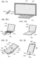
- FIGS. 7A , 7 B 1 , 7 B 2 , 7 C, and 7 D illustrate electronic devices
- FIG. 8 illustrates an electronic device
- FIGS. 9A and 9B illustrate lighting devices
- FIG. 10 illustrates a lighting device
- FIG. 11 illustrates in-vehicle display devices and lighting devices
- FIGS. 12A to 12C illustrate an electronic device
- FIG. 13 shows current density-luminance characteristics of a light-emitting element 1 and a comparative light-emitting element 1;
- FIG. 14 shows luminance-current efficiency characteristics of the light-emitting element 1 and the comparative light-emitting element 1;
- FIG. 15 shows luminance-power efficiency characteristics of the light-emitting element 1 and the comparative light-emitting element 1;
- FIG. 16 shows luminance-external quantum efficiency characteristics of the light-emitting element 1 and the comparative light-emitting element 1;
- FIG. 17 shows emission spectra of the light-emitting element 1 and the comparative light-emitting element 1.
- each component such as an anode, a layer containing an organic compound, a charge-generation layer, and a cathode are exaggerated for clarity in some cases. Therefore, the sizes of the components are not limited to the sizes in the drawings and relative sizes between the components.
- color is defined by three aspects of hue (corresponding to the wavelength of light of a single color), chroma (saturation, i.e., the degree to which it differs from white), and value (brightness, i.e., the intensity of light).
- hue corresponding to the wavelength of light of a single color
- chroma saturated, i.e., the degree to which it differs from white
- value blueness, i.e., the intensity of light
- color may be defined by only one of the above three aspects or two of the aspects which are selected arbitrarily.
- a difference between two colors of light means a difference in at least one of the above three aspects and includes a difference in the shapes of two spectra of light or in the distributions of the relative intensity of the peaks in the spectra.
- film and “layer” can be interchanged with each other depending on the case or circumstances.
- conductive layer can be changed into the term “conductive film” in some cases
- insulating film can be changed into the term “insulating layer” in some cases.
- a method for converting a triplet excited state into light emission there are a method utilizing phosphorescence, which is direct emission from a triplet excited state, and a method utilizing delayed fluorescence, which is light emitted from a singlet excited state after a triplet excited state is turned into a singlet excited state via reverse intersystem crossing.
- a structure of a light-emitting element that uses a phosphorescent material and emits light with extremely high efficiency has been reported, which actually proves advantages of the utilization of a triplet excited state for light emission.
- central metals of phosphorescent materials are mostly rare metals, and there are concerns about cost and supply in mass production.
- a substance emitting delayed fluorescence with relatively high efficiency has an extremely rare state where a singlet excited state and a triplet excited state are close to each other and accordingly has a unique molecular structure; thus, the kind of such a substance is still limited.
- an exciplex also called excited complex
- an exciplex is a complex in an excited state which is formed by two kinds of molecules due to charge-transfer interaction and that the singlet excited state and the triplet excited state of an exciplex are close to each other in many cases.
- an exciplex readily emits delayed fluorescence even at room temperature and might allow a fluorescent light-emitting element to have high efficiency.
- An emission wavelength of light emitted from an exciplex changes in accordance with a difference between a shallower HOMO level and a deeper LUMO level of the two kinds of substances that form the complex.
- light with a desired wavelength can be obtained relatively easily by selection of substances forming an exciplex.
- a light-emitting element in this embodiment includes a layer containing an organic compound (the layer may also contain an inorganic compound) between a pair of electrodes, and the layer containing an organic compound includes at least a light-emitting layer.
- the light-emitting layer contains a first organic compound having a hole-transport property and a second organic compound having an electron-transport property.
- a combination of the first organic compound and the second organic compound forms an exciplex when they are excited by a current or when a current flows therein.
- the HOMO level and LUMO level of the first organic compound are preferably shallower than the HOMO level and LUMO level of the second organic compound, respectively.
- the formation process of the exciplex is considered to be roughly classified into the following two processes.
- One formation process is the process in which an exciplex is formed by the first organic compound having a hole-transport property and the second organic compound having an electron-transport property which are in the state of having carriers (cation or anion).
- the other formation process is the process in which one of the first organic compound having a hole-transport property and the second organic compound having an electron-transport property forms a singlet exciton and then the singlet exciton interacts with the other in the ground state to form an exciplex.
- the exciplex in this embodiment may be formed by either process.
- the second organic compound having an electron-transport property has a structure in which a carbazole skeleton is bonded to a benzofuropyrimidine skeleton or a benzothienopyrimidine skeleton through a substituted or unsubstituted bivalent aromatic hydrocarbon group, light emission can be efficiently obtained from the exciplex. It is particularly preferable to use the benzofuropyrimidine skeleton to obtain light emission from the light-emitting element more efficiently.
- benzofuropyrimidine skeleton is more preferably used in formation of an exciplex than the benzothienopyrimidine skeleton since the LUMO level of the benzofuropyrimidine skeleton is slightly deeper than that of the benzothienopyrimidine skeleton.
- benzofuropyrimidine skeleton a benzofuro[3,2-d]pyrimidine skeleton is preferable
- benzothienopyrimidine skeleton a benzothieno[3,2-d]pyrimidine skeleton is preferable. This is because a benzene ring is introduced into the 6-position of pyrimidine in such skeletons, which improves an electron-transport property. Moreover, the LUMO level of each of such skeletons is deeper than that of a pyrimidine skeleton, which is favorable for formation of an exciplex.
- the 4-position of the benzofuro[3,2-d]pyrimidine skeleton or the benzothieno[3,2-d]pyrimidine skeleton be bonded to the aromatic hydrocarbon group.
- the 4-position and the 6-position of pyrimidine are substituted, whereby the electron-transport property can be increased.
- the LUMO level becomes deeper, which is more favorable for formation of an exciplex.
- the 4-position of the benzofuro[3,2-d]pyrimidine skeleton or the benzothieno[3,2-d]pyrimidine skeleton be bonded to the aromatic hydrocarbon group and that the other positions be unsubstituted.
- the benzofuro[3,2-d]pyrimidine skeleton or the benzothieno[3,2-d]pyrimidine skeleton easily interacts with the first organic compound, whereby an exciplex is easily formed.
- the 9-position of the carbazole skeleton is preferably bonded to the aromatic hydrocarbon group. In that case, an electrochemically stable compound can be obtained.
- the bivalent aromatic hydrocarbon group preferably has 6 to 60 carbon atoms.
- a bivalent aromatic hydrocarbon group having 6 to 13 carbon atoms is more preferable because of its excellent sublimability.
- a biphenyldiyl group is preferable as such an aromatic hydrocarbon group.
- a 3,3′-biphenyldiyl group is more preferable.
- the bivalent aromatic hydrocarbon group is preferably bonded to a nitrogen atom in the carbazole skeleton.
- an alkyl group having 1 to 6 carbon atoms and an aryl group having 6 to 12 carbon atoms are given as examples of the substituent.
- the second organic compound can be represented by the following general formula (G1).
- each of R 1 to R 5 independently represents any one of hydrogen, an alkyl group having 1 to 6 carbon atoms, a substituted or unsubstituted monocyclic saturated hydrocarbon having 5 to 7 carbon atoms, a substituted or unsubstituted polycyclic saturated hydrocarbon having 7 to 10 carbon atoms, and a substituted or unsubstituted aryl group having 6 to 13 carbon atoms.
- ac represents a substituted or unsubstituted aromatic hydrocarbon group
- n is an integer of 1 to 4.
- Cz represents a carbazole skeleton.
- X represents any one of an oxygen atom and a sulfur atom.
- the second organic compound can also be represented by the following general formula (G2).
- each of R 1 to R 13 independently represents any one of hydrogen, an alkyl group having 1 to 6 carbon atoms, a substituted or unsubstituted monocyclic saturated hydrocarbon having 5 to 7 carbon atoms, a substituted or unsubstituted polycyclic saturated hydrocarbon having 7 to 10 carbon atoms, and a substituted or unsubstituted aryl group having 6 to 13 carbon atoms.
- ⁇ represents a substituted or unsubstituted aromatic hydrocarbon group
- n is an integer of 1 to 4.
- X represents any one of an oxygen atom and a sulfur atom.
- a light-emitting element containing, as the second organic compound, 4- ⁇ 3-[3′-(9H-carbazol-9-yl)]biphenyl-3-yl ⁇ benzofuro[3,2-d]pyrimidine (abbreviation: 4mCzBPBfpm) represented by the following structural formula (100) has extremely high emission efficiency. Accordingly, 4mCzBPBfpm can be an extremely useful material for a light-emitting element in which an exciplex is used.
- a substituent includes a substituent, an alkyl group having 1 to 6 carbon atoms, a phenyl group, or a biphenyl group can be used as the substituent of the substituent.
- second organic compound can be represented by the following structural formulae (100) to (112) and structural formulae (200) to (212). Note that the second organic compound that can be used in this embodiment is not limited to the following examples.
- the triplet excitation energy of each of the first organic compound and the second organic compound (energy equivalent to a difference between a triplet excited level and a singlet excited level) be higher than the triplet excitation energy of the exciplex. This is because when the triplet excitation energy of each of the first organic compound and the second organic compound is lower than that of the exciplex, the triplet excitation energy of the exciplex is transferred, which inhibits efficient light emission.
- the first organic compound and the second organic compound not have a naphthalene skeleton.
- triplet excitation energy of an exciplex whose singlet excited state and triplet excited state has a small energy difference, can be considered equivalent to the emission wavelength of the exciplex.
- the first organic compound having a hole-transport property for example, a compound having a pyrrole ring, a thiophene ring, or a furan ring, a ⁇ -electron rich heteroaromatic compound such as a carbazole derivative or an indole derivative, or an aromatic amine compound is preferably used.
- An aromatic amine compound is particularly preferable because it can efficiently form an exciplex.
- Specific examples include compounds having aromatic amine skeletons, such as 2-[N-(9-phenylcarbazol-3-yl)-N-phenylamino]spiro-9,9′-bifluorene (abbreviation: PCASF), 4,4′-4′′-tris[N-(1-naphthyl)-N-phenylamino]triphenylamine (abbreviation: 1′-TNATA), 2,7-bis[N-(4-diphenylaminophenyl)-N-phenylamino]-spiro-9,9′-bifluorene (abbreviation: DPA2SF), N,N′-bis(9-phenylcarbazol-3-yl)-N,N′-diphenylbenzene-1,3-diamine (abbreviation: PCA2B), N-(9,9-dimethyl-2-diphenylamino-9H-fluoren-7-yl)diphenylamine
- An exciplex formed by the first organic compound and the second organic compound described above can emit light with extremely high efficiency; accordingly, the light-emitting element in this embodiment can emit light with high efficiency.
- the theoretical limit of external quantum efficiency of a fluorescent light-emitting element is generally considered to be approximately 5% to 7% when it is not designed to enhance extraction efficiency, a light-emitting element having external quantum efficiency higher than the theoretical limit can be easily provided with the use of the structure of the light-emitting element in this embodiment.
- the emission wavelength of an exciplex is equivalent to a difference between a shallower HOMO level and a deeper LUMO level of the first and second organic compounds, a light-emitting element emitting light with a desired wavelength can be easily provided by selection of substances each of which has an appropriate level.
- a highly efficient light-emitting element capable of converting a triplet excited state into light emission can be easily provided without a rare metal the supply of which is unstable.
- light-emitting elements with such characteristics can be provided without severe limitation on their emission wavelengths.
- one embodiment of the present invention has been described. Other embodiments of the present invention are described in other embodiments. Note that one embodiment of the present invention is not limited to the above examples. Although the case where a carbazole skeleton is bonded to a benzofuropyridyl group or a benzothienopyridyl group through an aromatic hydrocarbon group is described as one embodiment of the present invention, one embodiment of the present invention is not limited thereto. In one embodiment of the present invention, a structure other than the structure in which a carbazole skeleton is bonded to a benzofuropyridyl group or a benzothienopyridyl group through an aromatic hydrocarbon group may be used depending on the case and the condition.
- a structure in which a carbazole skeleton is bonded to a benzofuropyridyl group or a benzothienopyridyl group through an aromatic hydrocarbon group is not necessarily used depending on the case and the condition.
- Embodiment 1 a detailed example of the structure of the light-emitting element described in Embodiment 1 will be described below with reference to FIGS. 1A and 1B .
- the light-emitting element includes a first electrode 101 , a second electrode 102 , and a layer 103 containing an organic compound and provided between the first electrode 101 and the second electrode 102 .
- the first electrode 101 functions as an anode
- the second electrode 102 functions as a cathode.
- the layer 103 containing an organic compound includes at least a light-emitting layer 113 .
- a hole-injection layer Ill, a hole-transport layer 112 , an electron-transport layer 114 , and an electron-injection layer 115 which are illustrated in FIG. 1A are merely examples and not necessarily provided. A layer having any other function may also be provided.
- the first electrode 101 functions as the anode and is preferably formed using any of metals, alloys, electrically conductive compounds having a high work function (specifically, a work function of 4.0 eV or more), mixtures thereof, and the like.
- a work function of 4.0 eV or more specific examples are indium oxide-tin oxide (ITO: indium tin oxide), indium oxide-tin oxide containing silicon or silicon oxide, indium oxide-zinc oxide, indium oxide containing tungsten oxide and zinc oxide (IWZO), and the like.
- ITO indium oxide-tin oxide
- IWZO indium oxide-zinc oxide
- Such conductive metal oxide films are usually formed by a sputtering method, but may also be formed by application of a sol-gel method or the like.
- indium oxide-zinc oxide can be deposited by a sputtering method using a target in which zinc oxide is added to indium oxide at greater than or equal to 1 wt % and less than or equal to 20 wt %.
- indium oxide containing tungsten oxide and zinc oxide (IWZO) can be deposited by a sputtering method using a target in which, to indium oxide, tungsten oxide is added at greater than or equal to 0.5 wt % and less than or equal to 5 wt % and zinc oxide is added at greater than or equal to 0.1 wt % and less than or equal to 1 wt %.
- gold Au
- platinum Pt
- nickel Ni
- tungsten W
- Cr chromium
- Mo molybdenum
- iron Fe
- Co cobalt
- Cu copper
- palladium Pd
- a nitride of a metal material such as titanium nitride
- an electrode material can be selected regardless of its work function.
- the layer 103 containing an organic compound can be formed by combining a hole-injection layer, a hole-transport layer, a light-emitting layer, an electron-transport layer, an electron-injection layer, a carrier-blocking layer, a charge-generation layer, and the like as appropriate.
- the layer 103 containing an organic compound has a structure in which the hole-injection layer 111 , the hole-transport layer 112 , the light-emitting layer 113 , the electron-transport layer 114 , and the electron-injection layer 115 are stacked in this order over the first electrode 101 .
- Materials for the layers are specifically given below.
- the hole-injection layer 111 is a layer containing a substance having a high hole-injection property. Molybdenum oxide, vanadium oxide, ruthenium oxide, tungsten oxide, manganese oxide, or the like can be used. Alternatively, the hole-injection layer 111 can be formed using a phthalocyanine-based compound such as phthalocyanine (abbreviation: H 2 Pc) or copper phthalocyanine (abbreviation: CuPc), an aromatic amine compound such as 4,4′-bis[N-(4-diphenylaminophenyl)-N-phenylamino]biphenyl (abbreviation: DPAB) or N,N′-bis ⁇ 4-[bis(3-methylphenyl)amino]phenyl ⁇ -N,N′-diphenyl-(1,1′-biphenyl)-4,4′-diamine (abbreviation: DNTPD), a high molecular compound such as poly(3,
- a composite material in which a material having a hole-transport property contains a substance having an acceptor property can be used for the hole-injection layer 111 .
- a material having a hole-transport property which contains a substance having an acceptor property enables selection of a material used to form an electrode regardless of its work function.
- a material having a low work function can also be used for the first electrode 101 .
- the substance having an acceptor property 7,7,8,8-tetracyano-2,3,5,6-tetrafluoroquinodimethane (abbreviation: F 4 -TCNQ), chloranil, and the like can be given.
- transition metal oxides can be given.
- oxides of metals belonging to Group 4 to Group 8 of the periodic table can be given.
- vanadium oxide, niobium oxide, tantalum oxide, chromium oxide, molybdenum oxide, tungsten oxide, manganese oxide, and rhenium oxide are preferable because of their high electron-accepting properties.
- molybdenum oxide is especially preferable because it is stable in the air, has a low hygroscopic property, and is easily handled.
- any of a variety of organic compounds such as aromatic amine compounds, carbazole derivatives, aromatic hydrocarbons, and high molecular compounds (e.g., oligomers, dendrimers, or polymers) can be used.
- the organic compound used for the composite material is preferably an organic compound having a high hole-transport property. Specifically, a substance having a hole mobility of 10 ⁇ 6 cm 2 /Vs or higher is preferably used. Organic compounds which can be used as the material having a hole-transport property in the composite material are specifically given below.
- aromatic amine compound examples include N,N′-di(p-tolyl)-N,N′-diphenyl-p-phenylenediamine (abbreviation: DTDPPA), 4,4′-bis[N-(4-diphenylaminophenyl)-N-phenylamino]biphenyl (abbreviation: DPAB), N,N′-bis ⁇ 4-[bis(3-methylphenyl)amino]phenyl ⁇ -N,N′-diphenyl-(1,1′-biphenyl)-4,4′-diamine (abbreviation: DNTPD), 1,3,5-tris[N-(4-diphenylaminophenyl)-N-phenylamino]benzene (abbreviation: DPA3B), and the like.
- DTDPPA 4,4′-bis[N-(4-diphenylaminophenyl)-N-phenylamino]biphenyl
- carbazole derivative which can be used for the composite material are PCzPCA1, PCzPCA2, 3-[N-(1-naphthyl)-N-(9-phenylcarbazol-3-yl)amino]-9-phenylcarbazole (abbreviation: PCzPCN1), and the like.
- examples of the carbazole derivative which can be used for the composite material include CBP, 1,3,5-tris[4-(N-carbazolyl)phenyl]benzene (abbreviation: TCPB), 9-[4-(10-phenyl-9-anthryl)phenyl]-9H-carbazole (abbreviation: CzPA), 1,4-bis[4-(N-carbazolyl)phenyl]-2,3,5,6-tetraphenylbenzene, and the like.
- CBP 1,3,5-tris[4-(N-carbazolyl)phenyl]benzene
- CzPA 9-[4-(10-phenyl-9-anthryl)phenyl]-9H-carbazole
- 1,4-bis[4-(N-carbazolyl)phenyl]-2,3,5,6-tetraphenylbenzene, and the like CBP, 1,3,5-tris[4-(N-carbazoly
- the aromatic hydrocarbon which can be used for the composite material may have a vinyl skeleton.
- the aromatic hydrocarbon having a vinyl group include 4,4′-bis(2,2-diphenylvinyl)biphenyl (abbreviation: DPVBi), 9,10-bis[4-(2,2-diphenylvinyl)phenyl]anthracene (abbreviation: DPVPA), and the like.
- a high molecular compound such as poly(N-vinylcarbazole) (abbreviation: PVK), poly(4-vinyltriphenylamine) (abbreviation: PVTPA), poly[N-(4- ⁇ N′-[4-(4-diphenylamino)phenyl]phenyl-N′-phenylamino ⁇ phenyl)methacrylamide](abbreviation: PTPDMA), or poly[N,N′-bis(4-butylphenyl)-N,N′-bis(phenyl)benzidine](abbreviation: poly-TPD) can also be used.
- PVK poly(N-vinylcarbazole)
- PVTPA poly(4-vinyltriphenylamine)
- PTPDMA poly[N-(4- ⁇ N′-[4-(4-diphenylamino)phenyl]phenyl-N′-phenylamino ⁇ phenyl)methacrylamide]
- a hole-injection layer By providing a hole-injection layer, a high hole-injection property can be achieved to allow a light-emitting element to be driven at a low voltage.
- the hole-transport layer is a layer containing a material having a hole-transport property.
- the material having a hole-transport property include aromatic amine compounds such as NPB, TPD, 4,4′,4′′-tris(N,N-diphenylamino)triphenylamine (abbreviation: TDATA), 4,4′,4′′-tris[N-(3-methylphenyl)-N-phenylamino]triphenylamine (abbreviation: MTDATA), BSPB, BPAFLP, and the like.
- TDATA 4,4′,4′′-tris(N,N-diphenylamino)triphenylamine
- MTDATA 4,4′,4′′-tris[N-(3-methylphenyl)-N-phenylamino]triphenylamine
- BSPB 4,4′,4′′-tris[N-(3-methylphenyl)-N-phenylamino]triphenylamine
- BPAFLP BP
- the organic compounds given as the examples of the material having a hole-transport property in the composite material described above can also be used for the hole-transport layer.
- a high molecular compound such as PVK or PVTPA can also be used.
- the layer containing a material having a hole-transport property is not limited to a single layer, and may be a stack of two or more layers containing any of the above substances.
- the light-emitting layer 113 contains the first organic compound having a hole-transport property and the second organic compound having an electron-transport property.
- the light-emitting layer 113 may further contain a fluorescent substance. Materials and structures of the compounds are described in Embodiment 1. By having such a structure, the light-emitting element of this embodiment has extremely high external quantum efficiency though it is a fluorescent light-emitting element which does not use a rare metal.
- the light-emitting element also has an advantage in that its emission wavelength can be easily adjusted and thus light in desired wavelength ranges can be easily obtained with the efficiency kept high.
- the electron-transport layer 114 is a layer containing a material having an electron-transport property.
- the electron-transport layer 114 is formed using a metal complex having a quinoline skeleton or a benzoquinoline skeleton, such as tris(8-quinolinolato)aluminum (abbreviation: Alq), tris(4-methyl-8-quinolinolato)aluminum (abbreviation: Almq 3 ), bis(10-hydroxybenzo[h]quinolinato)beryllium (abbreviation: BeBq 2 ), or bis(2-methyl-8-quinolinolato)(4-phenylphenolato)aluminum (abbreviation: BAlq), or the like.
- a metal complex having a quinoline skeleton or a benzoquinoline skeleton such as tris(8-quinolinolato)aluminum (abbreviation: Alq), tris(4-methyl-8-quinolinola
- a metal complex having an oxazole-based or thiazole-based ligand such as bis[2-(2-hydroxyphenyl)benzoxazolato]zinc (abbreviation: Zn(BOX) 2 ) or bis[2-(2-hydroxyphenyl)benzothiazolato]zinc (abbreviation: Zn(BTZ) 2 ), or the like can also be used.
- Zn(BOX) 2 bis[2-(2-hydroxyphenyl)benzoxazolato]zinc
- Zn(BTZ) 2 bis[2-(2-hydroxyphenyl)benzothiazolato]zinc
- 2-(4-biphenylyl)-5-(4-tert-butylphenyl)-1,3,4-oxadiazole (abbreviation: PBD), 1,3-bis[5-(p-tert-butylphenyl)-1,3,4-oxadiazol-2-yl]benzene (abbreviation: OXD-7), 3-(4-biphenylyl)-4-phenyl-5-(4-tert-butylphenyl)-1,2,4-triazole (abbreviation: TAZ), bathophenanthroline (abbreviation: BPhen), bathocuproine (abbreviation: BCP), or the like can also be used.
- PBD 2-(4-biphenylyl)-5-(4-tert-butylphenyl)-1,3,4-oxadiazole
- OXD-7 1,3-bis[5-(p-tert-butylphenyl)-1,3,4-oxadiazol
- the substances mentioned here have high electron-transport properties and are mainly ones that have an electron mobility of 10 ⁇ 6 cm 2 /Vs or higher. Note that any of the above-described second organic compounds having electron-transport properties may be used for the electron-transport layer 114 .
- the electron-transport layer 114 is not limited to a single layer, and may be a stack of two or more layers containing any of the above substances.
- a layer that controls transfer of electron carriers may be provided.
- This is a layer formed by addition of a small amount of a substance having a high electron-trapping property to the aforementioned materials having a high electron-transport property, and the layer is capable of adjusting carrier balance by suppressing transfer of electron carriers.
- Such a structure is very effective in preventing a problem (such as a reduction in element lifetime) caused when electrons pass through the light-emitting layer.
- the electron-injection layer 115 may be provided in contact with the second electrode 102 between the electron-transport layer 114 and the second electrode 102 .
- an alkali metal, an alkaline earth metal, or a compound thereof such as lithium fluoride (LiF), cesium fluoride (CsF), or calcium fluoride (CaF 2 ).
- a layer that is formed using a substance having an electron-transport property and contains an alkali metal, an alkaline earth metal, or a compound thereof can be used.
- a layer that is formed using a substance having an electron-transport property and contains an alkali metal or an alkaline earth metal is preferably used as the electron-injection layer 115 , in which case electron injection from the second electrode 102 is efficiently performed.
- any of metals, alloys, electrically conductive compounds, and mixtures thereof which have a low work function (specifically, a work function of 3.8 eV or less) or the like can be used.
- a cathode material are elements belonging to Groups 1 and 2 of the periodic table, such as alkali metals (e.g., lithium (Li) and cesium (Cs)), magnesium (Mg), calcium (Ca), and strontium (Sr), alloys thereof (e.g., MgAg and AlLi), rare earth metals such as europium (Eu) and ytterbium (Yb), alloys thereof, and the like.
- any of a variety of conductive materials such as Al, Ag, ITO, or indium oxide-tin oxide containing silicon or silicon oxide can be used regardless of the work function. Films of these conductive materials can be formed by a sputtering method, an inkjet method, a spin coating method, or the like.
- any of a variety of methods can be used to form the layer 103 containing an organic compound regardless of whether it is a dry process or a wet process.
- a vacuum evaporation method, an inkjet method, a spin coating method, or the like may be used.
- Different formation methods may be used for the electrodes or the layers.
- the electrodes may be formed by a wet process using a sol-gel method, or by a wet process using paste of a metal material.
- the electrode may be formed by a dry process such as a sputtering method or a vacuum evaporation method.
- the light-emitting element having the above-described structure, current flows due to a potential difference between the first electrode 101 and the second electrode 102 , and holes and electrons recombine in the light-emitting layer 113 which contains a substance having a high light-emitting property, so that light is emitted. In other words, a light-emitting region is formed in the light-emitting layer 113 .
- first electrode 101 and the second electrode 102 Light emission is extracted out through one or both of the first electrode 101 and the second electrode 102 . Therefore, one or both of the first electrode 101 and the second electrode 102 are light-transmitting electrodes. In the case where only the first electrode 101 is a light-transmitting electrode, light emission is extracted through the first electrode 101 . In the case where only the second electrode 102 is a light-transmitting electrode, light emission is extracted through the second electrode 102 . In the case where both the first electrode 101 and the second electrode 102 are light-transmitting electrodes, light emission is extracted through the first electrode 101 and the second electrode 102 .
- the structure of the layers provided between the first electrode 101 and the second electrode 102 is not limited to the above-described structure.
- a light-emitting region where holes and electrons recombine is positioned away from the first electrode 101 and the second electrode 102 so that quenching due to the proximity of the light-emitting region and a metal used for electrodes and carrier-injection layers can be prevented.
- the hole-transport layer and the electron-transport layer which are in contact with the light-emitting layer 113 are formed using a substance having a wider band gap than the exciplex included in the light-emitting layer.
- FIG. 1B shows a light-emitting element having a structure different from FIG. 1A .
- a light-emitting element in which a plurality of light-emitting units is stacked hereinafter, also referred to as a stacked-layer element
- This light-emitting element is a light-emitting element including a plurality of light-emitting units between a first electrode and a second electrode.
- One light-emitting unit has a structure similar to that of the layer 103 containing an organic compound, which is illustrated in FIG. 1A .
- the light-emitting element illustrated in FIG. 1A includes a single light-emitting unit; the light-emitting element illustrated in FIG. 1B includes a plurality of light-emitting units.
- a first light-emitting unit 511 and a second light-emitting unit 512 are stacked between a first electrode 501 and a second electrode 502 , and a charge-generation layer 513 is provided between the first light-emitting unit 511 and the second light-emitting unit 512 .
- the first electrode 501 and the second electrode 502 correspond, respectively, to the first electrode 101 and the second electrode 102 illustrated in FIG. 1A , and the materials given in the description for FIG. 1A can be used.
- the first light-emitting unit 511 and the second light-emitting unit 512 may have the same structure or different structures.
- the charge-generation layer 513 contains a composite material of an organic compound and a metal oxide.
- this composite material of an organic compound and a metal oxide the composite material that can be used for the hole-injection layer illustrated in FIG. 1A can be used.
- the organic compound a variety of compounds such as an aromatic amine compound, a carbazole compound, an aromatic hydrocarbon, and a high molecular compound (such as an oligomer, a dendrimer, or a polymer) can be used.
- An organic compound having a hole mobility of 1 ⁇ 10 ⁇ 6 cm 2 /Vs or higher is preferably used. Note that any other substance may be used as long as the substance has a hole-transport property higher than an electron-transport property.
- the composite material of the organic compound and the metal oxide can achieve low-voltage driving and low-current driving because of the superior carrier-injection property and carrier-transport property.
- a hole-transport layer is not necessarily provided because the charge-generation layer can also function as the hole-transport layer.
- the charge-generation layer 513 may have a stacked-layer structure of a layer containing the composite material of an organic compound and a metal oxide and a layer containing another material.
- a stacked-layer structure of a layer containing the composite material of an organic compound and a metal oxide and a layer containing a compound selected from electron-donating substances and a compound having a high electron-transport property may be formed.
- a layer containing the composite material of an organic compound and a metal oxide may be stacked with a transparent conductive film.
- the charge-generation layer 513 provided between the first light-emitting unit 511 and the second light-emitting unit 512 may have any structure as long as electrons can be injected to a light-emitting unit on one side and holes can be injected to a light-emitting unit on the other side when a voltage is applied between the first electrode 501 and the second electrode 502 .
- any layer can be used as the charge-generation layer 513 as long as the layer injects electrons to the first light-emitting unit 511 and holes to the second light-emitting unit 512 when a voltage is applied such that the potential of the first electrode 501 is higher than that of the second electrode 502 .
- the light-emitting element having two light-emitting units is described with reference to FIG. 1B ; however, the present invention can be similarly applied to a light-emitting element in which three or more light-emitting units are stacked.
- a plurality of light-emitting units partitioned by the charge-generation layer between a pair of electrodes as in the light-emitting element illustrated in FIG. 1B it is possible to provide a light-emitting element which can emit light with high luminance with the current density kept low and has a long lifetime.
- a low-power-consumption light-emitting device which can be driven at low voltage can be achieved.
- emission colors of light-emitting units are made different, light emission of a desired color can be provided from the light-emitting element as a whole.
- the emission colors of the first light-emitting unit may be red and green and the emission color of the second light-emitting unit may be blue, so that the light-emitting element can emit white light as the whole element.
- the light-emitting element in this embodiment is preferably fabricated over a substrate of glass, plastic, or the like. As the way of stacking layers over the substrate, layers may be sequentially stacked from the first electrode 101 side or sequentially stacked from the second electrode 102 side.
- a light-emitting device although one light-emitting element may be formed over one substrate, a plurality of light-emitting elements may be formed over one substrate. With a plurality of light-emitting elements as described above formed over one substrate, a lighting device in which elements are separated or a passive matrix light-emitting device can be manufactured.
- a transistor may be formed over a substrate made of glass, plastic, or the like, and a light-emitting element may be formed over an electrode that is electrically connected to the transistor.
- an active matrix light-emitting device in which the driving of the light-emitting element is controlled by the transistor can be manufactured.
- the structure of the transistor may be a top-gate structure or a bottom-gate structure, and is not limited to a particular structure.
- a forward staggered transistor or an inverted staggered transistor may be used.
- crystallinity of a semiconductor used for the transistor and an amorphous semiconductor or a crystalline semiconductor may be used.
- a driver circuit formed over an element substrate may be formed with both n-type and p-type transistors or with either n-type transistors or p-type transistors.
- Embodiment 1 a light-emitting device including the light-emitting element described in Embodiment 1 or Embodiment 2 is described.
- FIG. 2A is a top view illustrating the light-emitting device
- FIG. 2B is a cross-sectional view of FIG. 2A taken along lines A-B and C-D.
- This light-emitting device includes a driver circuit portion (source line driver circuit) 601 , a pixel portion 602 , and a driver circuit portion (gate line driver circuit) 603 , which control light emission of the light-emitting element and are denoted by dotted lines.
- a reference numeral 604 denotes a sealing substrate; 605 , a sealing material; and 607 , a space surrounded by the sealing material 605 .
- a lead wiring 608 is a wiring for transmitting signals to be input to the source line driver circuit 601 and the gate line driver circuit 603 and for receiving a video signal, a clock signal, a start signal, a reset signal, and the like from an FPC (flexible printed circuit) 609 serving as an external input terminal.
- FPC flexible printed circuit
- PWB printed wiring board
- the light-emitting device in the present specification includes, in its category, not only the light-emitting device itself but also a light-emitting device provided with an FPC or a PWB.
- the driver circuit portions and the pixel portion are formed over an element substrate 610 ; the source line driver circuit 601 , which is a driver circuit portion, and one pixel in the pixel portion 602 are illustrated here.
- CMOS circuit In the source line driver circuit 601 , a CMOS circuit is formed in which an n-channel transistor 623 and a p-channel transistor 624 are combined.
- the driver circuit may be formed with any of a variety of circuits formed using TFTs, such as a CMOS circuit, a PMOS circuit, or an NMOS circuit.
- CMOS circuit CMOS circuit
- PMOS circuit PMOS circuit
- NMOS circuit complementary metal-oxide circuit
- the present invention is not limited to this type and the driver circuit can be formed outside the substrate.
- the pixel portion 602 is formed with a plurality of pixels each including a switching transistor 611 , a current controlling transistor 612 , and a first electrode 613 electrically connected to a drain of the current controlling transistor 612 .
- An insulator 614 is formed to cover an end portion of the first electrode 613 .
- the insulator 614 is formed using a positive photosensitive acrylic resin film.
- the insulator 614 is formed to have a curved surface with curvature at its upper or lower end portion.
- the upper end portion of the insulator 614 preferably has a curved surface with a curvature radius (greater than or equal to 0.2 ⁇ m and less than or equal to 3 ⁇ m).
- a negative photosensitive resin or a positive photosensitive resin can be used as the insulator 614 .
- a layer 616 containing an organic compound and a second electrode 617 are formed over the first electrode 613 .
- a material used for the first electrode 613 functioning as an anode a material having a high work function is preferably used.
- a single-layer film of an ITO film, an indium tin oxide film containing silicon, an indium oxide film containing zinc oxide at 2 wt % to 20 wt %, a titanium nitride film, a chromium film, a tungsten film, a Zn film, a Pt film, or the like, a stack including a titanium nitride film and a film containing aluminum as its main component, a stack including three layers of a titanium nitride film, a film containing aluminum as its main component, and a titanium nitride film, or the like can be used.
- the stacked-layer structure enables low wiring resistance, favorable ohmic contact, and a function as an anode.
- the layer 616 containing an organic compound is formed by any of a variety of methods such as an evaporation method using an evaporation mask, an inkjet method, and a spin coating method.
- the layer 616 containing an organic compound has the structure described in Embodiment 1 or Embodiment 2.
- a low molecular compound or a high molecular compound including an oligomer or a dendrimer may be used.
- a material used for the second electrode 617 which is formed over the layer 616 containing an organic compound and functions as a cathode
- a material having a low work function e.g., Al, Mg, Li, Ca, or an alloy or a compound thereof, such as MgAg, MgIn, or AlLi
- a low work function e.g., Al, Mg, Li, Ca, or an alloy or a compound thereof, such as MgAg, MgIn, or AlLi
- a stack including a thin metal film and a transparent conductive film e.g., ITO, indium oxide containing zinc oxide at 2 wt % to 20 wt %, indium tin oxide containing silicon, or zinc oxide (ZnO) is preferably used for the second electrode 617 .
- ITO indium oxide containing zinc oxide at 2 wt % to 20 wt %, indium tin oxide containing silicon, or zinc oxide (ZnO)
- the light-emitting element is formed with the first electrode 613 , the layer 616 containing an organic compound, and the second electrode 617 .
- the light-emitting element has the structure described in Embodiment 1 or Embodiment 2.
- the pixel portion which includes a plurality of light-emitting elements, may include both the light-emitting element described in Embodiment 1 or Embodiment 2 and a light-emitting element having a different structure.
- the sealing substrate 604 is attached to the element substrate 610 with the sealing material 605 , so that the light-emitting element 618 is provided in the space 607 surrounded by the element substrate 610 , the sealing substrate 604 , and the sealing material 605 .
- the space 607 is filled with filler, and may be filled with an inert gas (such as nitrogen or argon) or the sealing material 605 .
- an inert gas such as nitrogen or argon
- the sealing substrate be provided with a recessed portion and a desiccant 625 be provided in the recessed portion, in which case deterioration due to influence of moisture can be inhibited.
- An epoxy-based resin or glass frit is preferably used for the sealing material 605 .
- the material preferably allows as little moisture and oxygen as possible to penetrate.
- a glass substrate, a quartz substrate, or a plastic substrate formed of fiber reinforced plastic (FRP), poly(vinyl fluoride) (PVF), polyester, acrylic, or the like can be used as the sealing substrate 604 .
- the light-emitting device which uses the light-emitting element described in Embodiment 1 or Embodiment 2 can be obtained.
- the light-emitting device in this embodiment is fabricated using the light-emitting element described in Embodiment 1 or Embodiment 2 and thus can have favorable characteristics. Specifically, since the light-emitting element described in Embodiment 1 or Embodiment 2 has favorable emission efficiency, the light-emitting device can have reduced power consumption. In addition, light in desired wavelength ranges can be easily provided by the light-emitting element described in Embodiment 1 or Embodiment 2, which makes it possible to provide a versatile light-emitting device.
- FIGS. 3A and 3B each illustrate an example of a light-emitting device in which full color display is achieved by formation of light-emitting elements exhibiting white light emission and with the use of coloring layers (color filters) and the like.
- coloring layers (a red coloring layer 1034 R, a green coloring layer 1034 G, and a blue coloring layer 1034 B) are provided on a transparent base material 1033 .
- a black layer (a black matrix) 1035 may be additionally provided.
- the transparent base material 1033 provided with the coloring layers and the black layer is positioned and fixed to the substrate 1001 .
- the coloring layers and the black layer may be covered with an overcoat layer 1036 .
- light emitted from part of the light-emitting layer does not pass through the coloring layers, while light emitted from the other part of the light-emitting layer passes through the coloring layers. Since light which does not pass through the coloring layers is white and light which passes through any one of the coloring layers is red, blue, or green, an image can be displayed using pixels of the four colors.
- FIG. 3B illustrates an example in which the coloring layers (the red coloring layer 1034 R, the green coloring layer 1034 G, and the blue coloring layer 1034 B) are provided between the gate insulating film 1003 and the first interlayer insulating film 1020 .
- the coloring layers may be provided between the substrate 1001 and the sealing substrate 1031 .
- the above-described light-emitting device is a light-emitting device having a structure in which light is extracted from the substrate 1001 side where the transistors are formed (a bottom emission structure), but may be a light-emitting device having a structure in which light is extracted from the sealing substrate 1031 side (a top emission structure).
- FIG. 4 is a cross-sectional view of a light-emitting device having a top emission structure.
- a substrate which does not transmit light can be used as the substrate 1001 .
- the process up to the step of forming a connection electrode which connects the TFT and the anode of the light-emitting element is performed in a manner similar to that of the light-emitting device having a bottom emission structure.
- a third interlayer insulating film 1037 is formed to cover an electrode 1022 .
- This insulating film may have a planarization function.
- the third interlayer insulating film 1037 can be formed using a material similar to that of the second interlayer insulating film, and can alternatively be formed using any of other known materials.
- the first electrodes 1024 W, 1024 R, 1024 G, and 1024 B of the light-emitting elements each function as an anode here, but may function as a cathode. Further, in the case of a light-emitting device having a top emission structure as illustrated in FIG. 4 , the first electrodes are preferably reflective electrodes.
- the layer 1028 containing an organic compound is formed to have a structure similar to the structure of the layer 103 containing an organic compound, which is described in Embodiment 1 or Embodiment 2, with which white light emission can be obtained.
- sealing can be performed with the sealing substrate 1031 on which the coloring layers (the red coloring layer 1034 R, the green coloring layer 1034 G, and the blue coloring layer 1034 B) are provided.
- the sealing substrate 1031 may be provided with the black layer (the black matrix) 1035 which is positioned between pixels.
- the coloring layers (the red coloring layer 1034 R, the green coloring layer 1034 G, and the blue coloring layer 1034 B) and the black layer (the black matrix) 1035 may be covered with an overcoat layer. Note that a light-transmitting substrate is used as the sealing substrate 1031 .
- full color display is performed using four colors of red, green, blue, and white is shown here, there is no particular limitation and full color display using three colors of red, green, and blue may be performed.
- the light-emitting device in this embodiment is manufactured using the light-emitting element described in Embodiment 1 or Embodiment 2 and thus can have favorable characteristics. Specifically, since the light-emitting element described in Embodiment 1 or Embodiment 2 has favorable emission efficiency, the light-emitting device can have reduced power consumption. In addition, light in desired wavelength ranges can be easily provided by the light-emitting element described in Embodiment 1 or Embodiment 2, which makes it possible to provide a versatile light-emitting device.
- FIGS. 5A and 5B illustrate a passive matrix light-emitting device manufactured using the present invention.
- FIG. 5A is a perspective view of the light-emitting device
- FIG. 5B is a cross-sectional view of FIG. 5A taken along line X-Y.
- a layer 955 containing an organic compound is provided between an electrode 952 and an electrode 956 over a substrate 951 .
- An end portion of the electrode 952 is covered with an insulating layer 953 .
- a partition layer 954 is provided over the insulating layer 953 .
- Sidewalls of the partition layer 954 slope such that the distance between both sidewalls is gradually narrowed toward the surface of the substrate.
- a cross section taken along the direction of the short side of the partition layer 954 is trapezoidal, and the lower side (a side which is in the same direction as a plane direction of the insulating layer 953 and in contact with the insulating layer 953 ) is shorter than the upper side (a side which is in the same direction as the plane direction of the insulating layer 953 and not in contact with the insulating layer 953 ).
- the partition layer 954 thus provided can prevent defects in the light-emitting element due to static electricity or the like.
- the passive matrix light-emitting device can also have lower power consumption by including the light-emitting element described in Embodiment 1 or Embodiment 2, which has favorable emission efficiency.
- light in desired wavelength ranges can be easily provided by the light-emitting element described in Embodiment 1 or Embodiment 2, which makes it possible to provide a versatile light-emitting device.
- the light-emitting devices can be suitably used as display devices for displaying images.
- FIG. 6B is a top view of the lighting device
- FIG. 6A is a cross-sectional view of FIG. 6B taken along line e-f.
- a first electrode 401 is formed over a substrate 400 which is a support and has a light-transmitting property.
- the first electrode 401 corresponds to the first electrode 101 in Embodiment 2.
- the first electrode 401 is formed using a material having a light-transmitting property.
- a pad 412 for applying voltage to a second electrode 404 is provided over the substrate 400 .
- a layer 403 containing an organic compound is formed over the first electrode 401 .
- the structure of the layer 403 containing an organic compound corresponds to, for example, the structure of the layer 103 containing an organic compound in Embodiment 2, or the structure in which the light-emitting units 511 and 512 and the charge-generation layer 513 are combined. For these structures, the description in Embodiment 2 can be referred to.
- a black layer (black matrix) 402 is also formed.
- the second electrode 404 is formed to cover the layer 403 containing an organic compound.
- the second electrode 404 corresponds to the second electrode 102 in Embodiment 2.
- the second electrode 404 is formed using a material having high reflectance when light is extracted through the first electrode 401 side.
- the second electrode 404 is connected to the pad 412 , whereby voltage is applied thereto.
- the lighting device described in this embodiment includes the light-emitting element including the first electrode 401 , the layer 403 containing an organic compound, and the second electrode 404 . Since the light-emitting element is inexpensive and excellent in durability, the lighting device in this embodiment can have high emission efficiency.
- the substrate 400 provided with the light-emitting element having the above structure is attached to a sealing substrate 407 with a sealing material 405 , whereby the lighting-emitting element is sealed.
- a space 408 is preferably in a reduced pressure.
- the extended parts can serve as external input terminals.
- An IC chip 420 mounted with a converter or the like may be provided over the external input terminals.
- the lighting device described in this embodiment includes the light-emitting element described in Embodiment 1 or Embodiment 2, the lighting device can have high emission efficiency.
- Examples of electronic devices each including the light-emitting element described in Embodiment 1 or Embodiment 2 are described.
- the light-emitting element described in Embodiment 1 or Embodiment 2 has high emission efficiency and accordingly, the electronic devices in this embodiment each of which includes the light-emitting element can have low power consumption.
- Examples of the electronic devices to which the above light-emitting element is applied include television devices (also referred to as TV or television receivers), monitors for computers and the like, cameras such as digital cameras and digital video cameras, digital photo frames, mobile phones (also referred to as cell phones or mobile phone devices), portable game machines, portable information terminals, audio playback devices, large game machines such as pachinko machines, and the like. Specific examples of these electronic devices are described below.
- FIG. 7A illustrates an example of a television device.
- a display portion 7103 is incorporated in a housing 7101 .
- the housing 7101 is supported by a stand 7105 .
- Images can be displayed on the display portion 7103 , and in the display portion 7103 , the light-emitting elements described in Embodiment 1 or Embodiment 2 are arranged in a matrix.
- the light-emitting elements can have high emission efficiency. Therefore, the television device including the display portion 7103 which is formed using the light-emitting elements can have low power consumption.
- the television device can be operated with an operation switch of the housing 7101 or a separate remote controller 7110 .
- operation keys 7109 of the remote controller 7110 channels and volume can be controlled and images displayed on the display portion 7103 can be controlled.
- the remote controller 7110 may be provided with a display portion 7107 for displaying data output from the remote controller 7110 .
- the television device is provided with a receiver, a modem, and the like. With the use of the receiver, general television broadcasting can be received. Moreover, when the television device is connected to a communication network with or without wires via the modem, one-way (from a sender to a receiver) or two-way (between a sender and a receiver or between receivers) information communication can be performed.
- FIG. 7 B 1 illustrates a computer, which includes a main body 7201 , a housing 7202 , a display portion 7203 , a keyboard 7204 , an external connection port 7205 , a pointing device 7206 , and the like. Note that this computer is manufactured using light-emitting elements arranged in a matrix in the display portion 7203 , which are the same as that described in Embodiment 1 or Embodiment 2.
- the computer illustrated in FIG. 7B 1 may have a structure illustrated in FIG. 7 B 2 .
- the computer illustrated in FIG. 7 B 2 is provided with a second display portion 7210 instead of the keyboard 7204 and the pointing device 7206 .
- the second display portion 7210 is a touchscreen, and input can be performed by operation of display for input on the second display portion 7210 with a finger or a dedicated pen.
- the second display portion 7210 can also display images other than the display for input.
- the display portion 7203 may also be a touchscreen. Connecting the two screens with a hinge can prevent troubles; for example, the screens can be prevented from being cracked or broken while the computer is being stored or carried.
- this computer is manufactured using light-emitting elements arranged in a matrix in the display portion 7203 , which are the same as that described in Embodiment 1 or Embodiment 2. Therefore, this computer having the display portion 7203 which is formed using the light-emitting elements consumes less power.
- FIG. 7C illustrates a portable game machine, which includes two housings, a housing 7301 and a housing 7302 , which are connected with a joint portion 7303 so that the portable game machine can be opened or folded.
- the housing 7301 incorporates a display portion 7304 including light-emitting elements each of which is described in Embodiment 1 or Embodiment 2 and which are arranged in a matrix
- the housing 7302 incorporates a display portion 7305 .
- a speaker portion 7306 includes a speaker portion 7306 , a recording medium insertion portion 7307 , an LED lamp 7308 , input units (an operation key 7309 , a connection terminal 7310 , a sensor 7311 (a sensor having a function of measuring force, displacement, position, speed, acceleration, angular velocity, rotational frequency, distance, light, liquid, magnetism, temperature, chemical substance, sound, time, hardness, electric field, current, voltage, electric power, radiation, flow rate, humidity, gradient, oscillation, odor, or infrared rays), and a microphone 7312 ), and the like.
- a sensor 7311 a sensor having a function of measuring force, displacement, position, speed, acceleration, angular velocity, rotational frequency, distance, light, liquid, magnetism, temperature, chemical substance, sound, time, hardness, electric field, current, voltage, electric power, radiation, flow rate, humidity, gradient, oscillation, odor, or infrared rays
- the structure of the portable game machine is not limited to the above as long as the display portion including the light-emitting elements each of which is described in Embodiment 1 or Embodiment 2 and which are arranged in a matrix is used as either the display portion 7304 or the display portion 7305 , or both, and the structure can include other accessories as appropriate.
- the portable game machine illustrated in FIG. 7C has a function of reading out a program or data stored in a storage medium to display it on the display portion, and a function of sharing information with another portable game machine by wireless communication.
- the portable game machine illustrated in FIG. 7C can have a variety of functions without limitation to the above.
- the portable game machine having the display portion 7304 can have low power consumption because the light-emitting elements described in Embodiment 1 or Embodiment 2 are used in the display portion 7304 .
- FIG. 7D illustrates an example of a mobile phone.
- the mobile phone is provided with a display portion 7402 incorporated in a housing 7401 , operation buttons 7403 , an external connection port 7404 , a speaker 7405 , a microphone 7406 , and the like.
- the mobile phone has the display portion 7402 including the light-emitting elements each of which is described in Embodiment 1 or Embodiment 2 and which are arranged in a matrix. Accordingly, the mobile phone can have low power consumption.
- the first mode is a display mode mainly for displaying images.
- the second mode is an input mode mainly for inputting data such as characters.
- the third mode is a display-and-input mode in which two modes of the display mode and the input mode are combined.
- a character input mode mainly for inputting characters is selected for the display portion 7402 so that characters displayed on a screen can be input.
- a sensing device which includes a sensor for sensing inclination, such as a gyroscope or an acceleration sensor, is provided inside the mobile phone
- the direction of the mobile phone is determined so that display on the screen of the display portion 7402 can be automatically switched.
- the screen modes are switched by touching the display portion 7402 or operating the operation buttons 7403 of the housing 7401 .
- the screen modes can be switched depending on the kinds of images displayed on the display portion 7402 . For example, when a signal of an image displayed on the display portion is a signal of moving image data, the screen mode is switched to the display mode. When the signal is a signal of text data, the screen mode is switched to the input mode.
- the screen mode when input by touching the display portion 7402 is not performed within a specified period while a signal detected by an optical sensor in the display portion 7402 is detected, the screen mode may be controlled so as to be switched from the input mode to the display mode.
- the display portion 7402 may function as an image sensor. For example, an image of a palm print, a fingerprint, or the like is taken by touch on the display portion 7402 with the palm or the finger, whereby personal authentication can be performed. Further, by providing a backlight or a sensing light source which emits near-infrared light in the display portion, an image of a finger vein, a palm vein, or the like can be taken.
- the application range of the light-emitting device including the light-emitting element described in Embodiment 1 or Embodiment 2 is extremely wide; therefore, the light-emitting device can be applied to electronic devices of a variety of fields.
- an electronic device having low power consumption can be obtained.
- FIG. 8 illustrates an example of a liquid crystal display device using the light-emitting element described in Embodiment 1 or Embodiment 2 for a backlight.
- the liquid crystal display device shown in FIG. 8 includes a housing 901 , a liquid crystal layer 902 , a backlight unit 903 , and a housing 904 .
- the liquid crystal layer 902 is connected to a driver IC 905 .
- the light-emitting element described in Embodiment 1 or Embodiment 2 is used for the backlight unit 903 , to which current is supplied through a terminal 906 .
- the light-emitting element described in Embodiment 1 or Embodiment 2 is used for the backlight of the liquid crystal display device; thus, the backlight can have reduced power consumption.
- the use of the light-emitting element described in Embodiment 1 or Embodiment 2 enables manufacture of a planar-emission lighting device and further a larger-area planar-emission lighting device; therefore, the backlight can be a larger-area backlight, and the liquid crystal display device can also be a larger-area device.
- the light-emitting device using the light-emitting element described in Embodiment 1 or Embodiment 2 can be thinner than a conventional one; accordingly, the display device can also be thinner.
- FIG. 9A illustrates an example in which the light-emitting element described in Embodiment 1 or Embodiment 2 is used for a table lamp which is a lighting device.
- the table lamp illustrated in FIG. 9A includes a housing 2001 and a light source 2002 , and the lighting device described in Embodiment 4 is used for the light source 2002 .
- FIG. 10 illustrates an example in which the light-emitting element described in Embodiment 1 or Embodiment 2 is used for an indoor lighting device 3001 . Since the light-emitting element described in Embodiment 1 or Embodiment 2 has low power consumption, a lighting device having low power consumption can be obtained. Further, since the light-emitting element described in Embodiment 1 or Embodiment 2 can have a large area, the light-emitting element can be used for a large-area lighting device. Furthermore, since the light-emitting element described in Embodiment 1 or Embodiment 2 is thin, the light-emitting element can be used for a lighting device having a reduced thickness.
- the light-emitting element described in Embodiment 1 or Embodiment 2 can also be used for an automobile windshield or an automobile dashboard.
- FIG. 11 illustrates one mode in which the light-emitting element described in Embodiment 1 or Embodiment 2 is used for an automobile windshield and an automobile dashboard.
- Display regions 5000 to 5005 each include the light-emitting element described in Embodiment 1 or Embodiment 2.
- the display region 5000 and the display region 5001 are display devices which are provided in the automobile windshield and in which the light-emitting element described in Embodiment 1 or Embodiment 2 is incorporated.
- the light-emitting element described in Embodiment 1 or Embodiment 2 can be formed into what is called a see-through display device, through which the opposite side can be seen, by including a first electrode and a second electrode formed of electrodes having light-transmitting properties.
- Such see-through display devices can be provided even in the automobile windshield, without hindering the vision.
- a transistor having a light-transmitting property such as an organic transistor using an organic semiconductor material or a transistor using an oxide semiconductor, is preferably used.
- the display region 5002 is a display device provided in a pillar portion in which the light-emitting elements described in Embodiment 1 or Embodiment 2 are incorporated.
- the display region 5002 can compensate for the view hindered by the pillar portion by showing an image taken by an imaging unit provided in the car body.
- the display region 5003 provided in the dashboard can compensate for the view hindered by the car body by showing an image taken by an imaging unit provided in the outside of the car body, which leads to elimination of blind areas and enhancement of safety. Showing an image so as to compensate for the area which a driver cannot see makes it possible for the driver to confirm safety easily and comfortably.
- the display region 5004 and the display region 5005 can provide a variety of kinds of information such as navigation data, a speedometer, a tachometer, a mileage, a fuel meter, a gearshift indicator, and air-condition setting.
- the content or layout of the display can be changed freely by a user as appropriate. Further, such information can also be shown by the display regions 5000 to 5003 . Note that the display regions 5000 to 5005 can also be used as lighting devices.
- the light-emitting element described in Embodiment 1 or Embodiment 2 can have low power consumption.
- the light-emitting device and the lighting device each of which includes the light-emitting element described in Embodiment 1 or Embodiment 2 can be suitably used as an in-vehicle light-emitting device and an in-vehicle lighting device.
- FIGS. 12A and 12B illustrate an example of a foldable tablet terminal.
- the tablet terminal is opened in FIG. 12A .
- the tablet terminal includes a housing 9630 , a display portion 9631 a , a display portion 9631 b , a display mode switch 9034 , a power switch 9035 , a power saver switch 9036 , a clasp 9033 , and an operation switch 9038 .
- the display portion 9631 a and the display portion 9631 b is/are formed using a light-emitting device which includes the light-emitting element described in Embodiment 1 or Embodiment 2.
- Part of the display portion 9631 a can be a touchscreen region 9632 a and data can be input when a displayed operation key 9637 is touched.
- half of the display portion 9631 a has only a display function and the other half has a touchscreen function
- one embodiment of the present invention is not limited to the structure.
- the whole display portion 9631 a may have a touchscreen function.
- a keyboard can be displayed on the entire region of the display portion 9631 a so that the display portion 9631 a is used as a touchscreen, and the display portion 9631 b can be used as a display screen.
- part of the display portion 9631 b can be a touchscreen region 9632 b .
- a switching button 9639 for showing/hiding a keyboard of the touchscreen is touched with a finger, a stylus, or the like, so that keyboard buttons can be displayed on the display portion 9631 b.
- Touch input can be performed in the touchscreen region 9632 a and the touchscreen region 9632 b at the same time.
- the display mode switch 9034 can switch the display between a portrait mode, a landscape mode, and the like, and between monochrome display and color display, for example.
- the luminance of display can be optimized in accordance with the amount of external light at the time when the tablet terminal is in use, which is detected with an optical sensor incorporated in the tablet terminal.
- the tablet terminal may include another sensing device such as a sensor for determining inclination (e.g., a gyroscope or an acceleration sensor) in addition to the optical sensor.
- FIG. 12A illustrates an example in which the display portion 9631 a and the display portion 9631 b have the same display area
- one embodiment of the present invention is not limited to the example.
- the display portion 9631 a and the display portion 9631 b may have different display areas and different display quality.
- one of them may be a display panel that can display higher-definition images than the other.
- the tablet terminal is folded in FIG. 12B .
- the tablet terminal includes the housing 9630 , a solar cell 9633 , a charge and discharge control circuit 9634 , a battery 9635 , and a DC-to-DC converter 9636 .
- FIG. 12B illustrates an example in which the charge and discharge control circuit 9634 includes the battery 9635 and the DC-to-DC converter 9636 .
- the housing 9630 can be closed when not in use.
- the display portions 9631 a and 9631 b can be protected, thereby providing a tablet terminal with excellent durability and excellent reliability for long-term use.
- the tablet terminal illustrated in FIGS. 12A and 12B can have a function of displaying various kinds of information (e.g., a still image, a moving image, and a text image) on the display portion, a function of displaying a calendar, the date, the time, or the like on the display portion, a touch input function of operating or editing information displayed on the display portion by touch input, a function of controlling processing by various kinds of software (programs), and the like.
- various kinds of information e.g., a still image, a moving image, and a text image
- the solar cell 9633 which is attached on the surface of the tablet terminal, supplies electric power to a touchscreen, a display portion, an image signal processor, and the like. Note that the solar cell 9633 is preferably provided on one or two surfaces of the housing 9630 , in which case the battery 9635 can be charged efficiently.
- FIG. 12C shows the solar cell 9633 , the battery 9635 , the DC-to-DC converter 9636 , a converter 9638 , switches SW 1 to SW 3 , and the display portion 9631 .
- the battery 9635 , the DC-to-DC converter 9636 , the converter 9638 , and the switches SW 1 to SW 3 correspond to the charge and discharge control circuit 9634 in FIG. 12B .
- the power generation unit is not particularly limited, and the battery 9635 may be charged by another power generation unit such as a piezoelectric element or a thermoelectric conversion element (Peltier element).
- the battery 9635 may be charged by a non-contact power transmission module which is capable of charging by transmitting and receiving power by wireless (without contact), or any of the other charge unit used in combination, and the power generation unit is not necessarily provided.
- One embodiment of the present invention is not limited to the tablet terminal having the shape illustrated in FIGS. 12A to 12C as long as the display portion 9631 is included.
- FIG. 9B Another example of the lighting device is illustrated in FIG. 9B .
- a desk lamp illustrated in FIG. 9B includes a lighting portion 9501 , a support 9503 , a support base 9505 , and the like.
- the lighting portion 9501 includes the light-emitting element of one embodiment of the present invention.
- a lighting device having a curved surface or having a flexible lighting portion can be provided.
- the use of a flexible light-emitting device for a lighting device as described above not only improves the degree of freedom in design of the lighting device but also enables the lighting device to be mounted on a portion having a curved surface, such as the ceiling or dashboard of an automobile.
- a lighting device can realize high emission efficiency.
- a lighting device with high reliability can be provided.
- a lighting device with low power consumption can be provided.
- the light-emitting element has a considerably wide application range, and can be applied to electronic devices in a variety of fields.
- the aqueous layer of the obtained reaction mixture was subjected to extraction with toluene, and the solution of the extract and the organic layer were combined and washed with water and a saturated aqueous solution of sodium chloride. Magnesium sulfate was added to the organic layer for drying, and the resulting mixture was subjected to gravity filtration to give a filtrate. This filtrate was concentrated to give an oily substance.
- the oily substance was purified by recycling preparative HPLC using LC-SakuraNEXT.
- Step 3 Synthesis of 4- ⁇ 3-[3′-(9H-carbazol-9-yl)]biphenyl-3-yl ⁇ benzofuro[3,2-d]pyrimidine (abbreviation: 4mCzBPBfpm)
- the solid was dissolved in toluene and this solution was filtered through Celite (produced by Wako Pure Chemical Industries, Ltd., Catalog No. 531-16855), alumina, and Celite. The filtrate was concentrated to give a solid.
- the solid was recrystallized from toluene, so that 2.0 g of a white solid was obtained in a yield of 50%.
- 2.0 g of the white solid was purified by sublimation using a train sublimation method.
- the sublimation purification was conducted under the conditions where the pressure was 2.3 Pa, the flow rate of an argon gas was 10 mL/min, and the solid was heated at 250° C. After the sublimation purification, 1.3 g of a white solid which was a target substance was obtained at a collection rate of 65%.
- the synthesis scheme of the step 3 is shown in (c-2) below.
- a light-emitting element (light-emitting element 1) of one embodiment of the present invention and a comparative light-emitting element (comparative light-emitting element 1) are described.
- the second organic compound in the light-emitting layer 113 4mCzBPBfpm (structural formula (100)) was used in the light-emitting element 1 and 4-[3′-(dibenzothiophen-4-yl)biphenyl-3-yl]benzofuro[3,2-d]pyrimidine (abbreviation: 4mDBTBPBfpm-II) (structural formula (v)) was used in the comparative light-emitting element 1.
- a surface of the ITSO was covered with a polyimide film so that an area of 2 mm ⁇ 2 mm of the surface was exposed. The electrode area was 2 mm ⁇ 2 mm.
- the surface of the substrate was washed with water and baked at 200° C. for 1 hour, and then a UV ozone treatment was performed for 370 seconds. Then, the substrate was transferred into a vacuum evaporation apparatus where the pressure was reduced to about 10 ⁇ 4 Pa, vacuum baking at 170° C. for 30 minutes was performed in a heating chamber of the vacuum evaporation apparatus, and then the substrate was cooled down for about 30 minutes.
- the substrate was fixed to a holder provided in the vacuum evaporation apparatus such that the surface of the substrate over which the first electrode 101 was formed faced downward.
- the hole-injection layer 111 , the hole-transport layer 112 , the light-emitting layer 113 , the electron-transport layer 114 , and the electron-injection layer 115 which were included in the layer 103 containing an organic compound, were sequentially formed by a vacuum evaporation method.
- DBT3P-II 4,4′,4′′-(benzene-1,3,5-triyl)tri(dibenzothiophene)
- molybdenum oxide was deposited by co-evaporation such that the mass ratio of DBT3P-II to molybdenum oxide was 2:1, whereby the hole-injection layer 111 was formed over the first electrode 101 .
- the thickness was set to 60 nm.
- a co-evaporation method is an evaporation method in which a plurality of different substances is concurrently vaporized from respective different evaporation sources.
- BPAFLP 4-phenyl-4′-(9-phenylfluoren-9-yl)triphenylamine
- the light-emitting layer 113 was formed over the hole-transport layer 112 .
- the light-emitting layer 113 was formed in the following manner: 4- ⁇ 3-[3′-(9H-carbazol-9-yl)]biphenyl-3-yl ⁇ benzofuro[3,2-d]pyrimidine (abbreviation: 4mCzBPBfpm) (structural formula (100)) and N-(1,1′-biphenyl-4-yl)-N-[4-(9-phenyl-9H-carbazol-3-yl)phenyl]-9,9-dimethyl-9H-fluoren-2-amine (abbreviation: PCBBiF) (structural formula (iii)) were deposited by co-evaporation to a thickness of 40 nm such that the mass ratio of 4mCzBPBfpm to PCBBiF was 0.8:0.2, and then, 4- ⁇ 3-[3′-(9H-carbazol-9-yl)]biphenyl-3-yl ⁇ benzofuro[3,2-d]pyrimidine (
- the electron-transport layer 114 was formed over the light-emitting layer 113 .
- Bathophenanthroline abbreviation: BPhen
- structural formula (iv) was deposited by evaporation to a thickness of 10 nm, so that the electron-transport layer 114 was formed.
- lithium fluoride was deposited by evaporation to a thickness of 1 nm over the electron-transport layer 114 , whereby the electron-injection layer 115 was formed.
- the light-emitting element 1 was obtained.
- the comparative light-emitting element 1 refer also to the fabrication method of the light-emitting element 1, since films other than the light-emitting layer 113 were formed using the same materials as those in the light-emitting element 1.
- the first electrode 101 of the comparative light-emitting element 1 was formed using ITSO to a thickness of 110 nm.
- the hole-injection layer 111 was formed by co-evaporation to a thickness of 20 nm so that the mass ratio of DBT3P-II to molybdenum oxide was 2:1.
- BPAFLP was deposited to a thickness of 20 nm.
- the light-emitting layer 113 was formed in the following manner: 4-[3′-(dibenzothiophen-4-yl)biphenyl-3-yl]benzofuro[3,2-d]pyrimidine (abbreviation: 4mDBTBPBfpm-II) (structural formula (v)) and PCBBiF were deposited by co-evaporation to a thickness of 40 nm such that the mass ratio of 4mDBTBPBfpm-II to PCBBiF was 0.8:0.2, and then, 4mDBTBPBfpm-II was deposited to a thickness of 10 nm. Next, BPhen was deposited by evaporation to a thickness of 15 nm, so that the electron-transport layer 114 was formed. The electron-injection layer 115 and the second electrode 102 were formed using the same materials and to the same thicknesses as those of the light-emitting element 1.
- FIG. 13 shows current density-luminance characteristics of the light-emitting elements
- FIG. 14 shows luminance-current efficiency characteristics of the light-emitting elements
- FIG. 15 shows luminance-power efficiency characteristics of the light-emitting elements
- FIG. 16 shows luminance-external quantum efficiency characteristics of the light-emitting elements
- FIG. 17 shows emission spectra.
- the light-emitting element 1 has more favorable luminance-current efficiency characteristics and luminance-external quantum efficiency characteristics than the comparative light-emitting element 1, which indicates that the light-emitting element 1 has high emission efficiency (high current efficiency and high external quantum efficiency). Moreover, the drive voltage of the light-emitting element 1 was low, and as a result, extremely high power efficiency as shown in FIG. 15 was achieved. Note that the difference between 4mCzBPBfpm used in the light-emitting element 1 and 4mDBTBPBfpm-II used in the comparative light-emitting element 1 is whether a carbazole skeleton or a dibenzothiophene skeleton is used.
- the triplet excitation level (T1 level) of 4mCzBPBfpm is estimated to be 2.68 eV (462 nm) from a phosphorescence spectrum peak at 10K.
- the T1 level of PCBBiF is estimated to be 2.44 eV (509 nm) in the same measurement.
- the T1 levels of 4mCzBPBfpm and PCBBiF are both higher than 2.26 eV (549 nm) which is the emission energy (singlet excitation level; S1 level) of the exciplex.
Landscapes
- Chemical & Material Sciences (AREA)
- Organic Chemistry (AREA)
- Engineering & Computer Science (AREA)
- Materials Engineering (AREA)
- Physics & Mathematics (AREA)
- Spectroscopy & Molecular Physics (AREA)
- Optics & Photonics (AREA)
- Manufacturing & Machinery (AREA)
- Electroluminescent Light Sources (AREA)
- Devices For Indicating Variable Information By Combining Individual Elements (AREA)
- Illuminated Signs And Luminous Advertising (AREA)
Priority Applications (1)
| Application Number | Priority Date | Filing Date | Title |
|---|---|---|---|
| US16/807,492 US20200227653A1 (en) | 2015-05-29 | 2020-03-03 | Light-Emitting Element, Light-Emitting Device, Display Device, Electronic Device, and Lighting Device |
Applications Claiming Priority (2)
| Application Number | Priority Date | Filing Date | Title |
|---|---|---|---|
| JP2015109756 | 2015-05-29 | ||
| JP2015-109756 | 2015-05-29 |
Related Child Applications (1)
| Application Number | Title | Priority Date | Filing Date |
|---|---|---|---|
| US16/807,492 Continuation US20200227653A1 (en) | 2015-05-29 | 2020-03-03 | Light-Emitting Element, Light-Emitting Device, Display Device, Electronic Device, and Lighting Device |
Publications (2)
| Publication Number | Publication Date |
|---|---|
| US20160351829A1 US20160351829A1 (en) | 2016-12-01 |
| US10586932B2 true US10586932B2 (en) | 2020-03-10 |
Family
ID=57397681
Family Applications (2)
| Application Number | Title | Priority Date | Filing Date |
|---|---|---|---|
| US15/166,585 Expired - Fee Related US10586932B2 (en) | 2015-05-29 | 2016-05-27 | Light-emitting element, light-emitting device, display device, electronic device, and lighting device |
| US16/807,492 Abandoned US20200227653A1 (en) | 2015-05-29 | 2020-03-03 | Light-Emitting Element, Light-Emitting Device, Display Device, Electronic Device, and Lighting Device |
Family Applications After (1)
| Application Number | Title | Priority Date | Filing Date |
|---|---|---|---|
| US16/807,492 Abandoned US20200227653A1 (en) | 2015-05-29 | 2020-03-03 | Light-Emitting Element, Light-Emitting Device, Display Device, Electronic Device, and Lighting Device |
Country Status (6)
| Country | Link |
|---|---|
| US (2) | US10586932B2 (https=) |
| JP (2) | JP6875074B2 (https=) |
| KR (1) | KR20180013958A (https=) |
| CN (3) | CN110600635A (https=) |
| TW (2) | TWI777294B (https=) |
| WO (1) | WO2016193845A1 (https=) |
Cited By (3)
| Publication number | Priority date | Publication date | Assignee | Title |
|---|---|---|---|---|
| US12268044B2 (en) | 2019-04-30 | 2025-04-01 | Samsung Display Co., Ltd. | Organic light-emitting device including a first exciplex and a second exciplex in an emission layer |
| US12274117B2 (en) | 2020-12-15 | 2025-04-08 | Samsung Display Co., Ltd. | Light-emitting device and an electronic apparatus including same |
| US12550606B2 (en) | 2018-03-22 | 2026-02-10 | Samsung Display Co., Ltd. | Organic light-emitting device and electronic apparatus including the same |
Families Citing this family (11)
| Publication number | Priority date | Publication date | Assignee | Title |
|---|---|---|---|---|
| KR20160007380A (ko) * | 2014-07-11 | 2016-01-20 | 가부시키가이샤 한도오따이 에네루기 켄큐쇼 | 발광 소자, 화합물, 디스플레이 모듈, 조명 모듈, 발광 장치, 표시 장치, 조명 장치, 및 전자 기기 |
| CN110600635A (zh) | 2015-05-29 | 2019-12-20 | 株式会社半导体能源研究所 | 发光元件、发光装置、显示装置、电子设备以及照明装置 |
| KR20250065420A (ko) * | 2015-12-25 | 2025-05-12 | 가부시키가이샤 한도오따이 에네루기 켄큐쇼 | 화합물, 발광 소자, 표시 장치, 전자 기기, 및 조명 장치 |
| KR102616441B1 (ko) | 2016-12-23 | 2023-12-26 | 가부시키가이샤 한도오따이 에네루기 켄큐쇼 | 유기 화합물, 발광 소자, 발광 장치, 전자 기기, 및 조명 장치 |
| DE112018001365T5 (de) | 2017-03-16 | 2019-11-28 | Semiconductor Energy Laboratory Co., Ltd. | Organische Verbindung, Licht emittierendes Element, Licht emittierende Vorrichtung, elektronisches Gerät und Beleuchtungsvorrichtung |
| JP2019006763A (ja) * | 2017-06-22 | 2019-01-17 | 株式会社半導体エネルギー研究所 | 有機化合物、発光素子、発光装置、電子機器、および照明装置 |
| TWI787279B (zh) | 2017-06-23 | 2022-12-21 | 日商半導體能源研究所股份有限公司 | 有機化合物、發光元件、發光裝置、電子裝置及照明設備 |
| CN119894227A (zh) | 2017-11-02 | 2025-04-25 | 株式会社半导体能源研究所 | 发光元件、显示装置、电子设备及照明装置 |
| KR102943367B1 (ko) | 2019-04-12 | 2026-03-24 | 가부시키가이샤 한도오따이 에네루기 켄큐쇼 | 유기 화합물, 발광 디바이스, 발광 장치, 전자 기기, 및 조명 장치 |
| US20210066617A1 (en) * | 2019-08-30 | 2021-03-04 | Samsung Display Co., Ltd. | Light-emitting device and electronic apparatus including the same |
| KR102919535B1 (ko) * | 2019-08-30 | 2026-02-02 | 삼성디스플레이 주식회사 | 발광 소자 및 이를 포함하는 전자 장치 |
Citations (47)
| Publication number | Priority date | Publication date | Assignee | Title |
|---|---|---|---|---|
| JPH06220059A (ja) | 1993-01-28 | 1994-08-09 | Tanabe Seiyaku Co Ltd | 縮合ピリミジン誘導体及びその製法 |
| EP1202608A2 (en) | 2000-10-30 | 2002-05-02 | Kabushiki Kaisha Toyota Chuo Kenkyusho | Organic light-emitting devices |
| US20030175553A1 (en) | 2001-12-28 | 2003-09-18 | Thompson Mark E. | White light emitting oleds from combined monomer and aggregate emission |
| US20050048310A1 (en) | 2001-07-13 | 2005-03-03 | Consiglio Nazionale Delle Ricerche | Organic electroluminescent device based upon emission of exciplexes or electroplexes, and a method for its fabrication |
| US20050221116A1 (en) | 2002-03-29 | 2005-10-06 | Massimo Cocchi | Organic electroluminescent device with chromophore dopants |
| US20060134464A1 (en) | 2004-12-22 | 2006-06-22 | Fuji Photo Film Co. Ltd | Organic electroluminescent element |
| US7175922B2 (en) | 2003-10-22 | 2007-02-13 | Eastman Kodak Company | Aggregate organic light emitting diode devices with improved operational stability |
| US7183010B2 (en) | 2002-04-24 | 2007-02-27 | Eastman Kodak Corporation | Organic light-emitting diode devices with improved operational stability |
| US20070090756A1 (en) | 2005-10-11 | 2007-04-26 | Fujifilm Corporation | Organic electroluminescent element |
| US7332857B2 (en) | 2001-01-18 | 2008-02-19 | Semiconductor Energy Laboratory Co., Ltd. | Light emitting device and manufacturing method thereof |
| JP2008288344A (ja) | 2007-05-16 | 2008-11-27 | Nippon Hoso Kyokai <Nhk> | 有機el素子 |
| US20080314965A1 (en) | 2007-06-23 | 2008-12-25 | Roberts Mark D | System and method for authentication of engineering notebook support information |
| US20090153034A1 (en) | 2007-12-13 | 2009-06-18 | Universal Display Corporation | Carbazole-containing materials in phosphorescent light emittinig diodes |
| US7597967B2 (en) | 2004-12-17 | 2009-10-06 | Eastman Kodak Company | Phosphorescent OLEDs with exciton blocking layer |
| JP2011084531A (ja) | 2009-10-19 | 2011-04-28 | Konica Minolta Holdings Inc | 有機エレクトロルミネッセンス素子用材料、有機エレクトロルミネッセンス素子、照明装置及び表示装置 |
| US7993760B2 (en) | 2005-12-01 | 2011-08-09 | Nippon Steel Chemical Co., Ltd. | Compound for use in organic electroluminescent device and organic electroluminescent device |
| US8034465B2 (en) | 2007-06-20 | 2011-10-11 | Global Oled Technology Llc | Phosphorescent oled having double exciton-blocking layers |
| US20120217487A1 (en) | 2011-02-28 | 2012-08-30 | Semiconductor Energy Laboratory Co., Ltd. | Light-Emitting Device |
| US8274214B2 (en) | 2008-09-01 | 2012-09-25 | Semiconductor Energy Laboratory Co., Ltd. | Light emitting element, light emitting device, and electronic device |
| US20130277656A1 (en) * | 2012-04-20 | 2013-10-24 | Semiconductor Energy Laboratory Co., Ltd. | Light-Emitting Element, Light-Emitting Device, Electronic Appliance, and Lighting Device |
| US8586204B2 (en) | 2007-12-28 | 2013-11-19 | Universal Display Corporation | Phosphorescent emitters and host materials with improved stability |
| US20140034932A1 (en) | 2012-08-03 | 2014-02-06 | Semiconductor Energy Laboratory Co., Ltd. | Light-Emitting Element, Light-Emitting Device, Electronic Device, and Lighting Device |
| US20140034929A1 (en) * | 2012-08-03 | 2014-02-06 | Semiconductor Energy Laboratory Co., Ltd. | Light-Emitting Element, Light-Emitting Device, Electronic Device, and Lighting Device |
| US8652652B2 (en) | 2007-08-08 | 2014-02-18 | Universal Display Corporation | Single triphenylene chromophores in phosphorescent light emitting diodes |
| WO2014065073A1 (ja) | 2012-10-22 | 2014-05-01 | コニカミノルタ株式会社 | 透明電極、電子デバイスおよび有機エレクトロルミネッセンス素子 |
| US8822708B2 (en) | 2007-08-08 | 2014-09-02 | Universal Display Corporation | Benzo-fused thiophene / triphenylene hybrid materials |
| US20140291643A1 (en) * | 2013-03-26 | 2014-10-02 | Semiconductor Energy Laboratory Co., Ltd. | Organic Compound, Light-Emitting Element, Light-Emitting Device, Display Device, Electronic Device, and Lighting Device |
| US20140291645A1 (en) | 2013-03-26 | 2014-10-02 | Semiconductor Energy Laboratory Co., Ltd. | Light-Emitting Element, Compound, Organic Compound, Display Module, Lighting Module, Light-Emitting Device, Display Device, Lighting Device, and Electronic Device |
| JP2014192214A (ja) | 2013-03-26 | 2014-10-06 | Semiconductor Energy Lab Co Ltd | 発光素子、発光装置、表示装置、電子機器及び照明装置 |
| US8853680B2 (en) | 2011-03-30 | 2014-10-07 | Semiconductor Energy Laboratory Co., Ltd. | Light-emitting element |
| US8866377B2 (en) | 2006-12-28 | 2014-10-21 | Universal Display Corporation | Long lifetime phosphorescent organic light emitting device (OLED) structures |
| US20140319492A1 (en) | 2013-04-26 | 2014-10-30 | Semiconductor Energy Laboratory Co., Ltd. | Light-Emitting Element, Light-Emitting Device, Display Device, Electronic Device, and Lighting Device |
| US8963127B2 (en) | 2009-11-24 | 2015-02-24 | Lg Display Co., Ltd. | White organic light emitting device |
| US20150069352A1 (en) | 2012-04-10 | 2015-03-12 | Snu R&Db Foundation | Organic light-emitting diode containing co-hosts forming exciplex, and lighting device and display apparatus including same |
| US8981355B2 (en) | 2012-02-09 | 2015-03-17 | Semiconductor Energy Laboratory Co., Ltd. | Light-emitting element |
| WO2015037675A1 (ja) | 2013-09-11 | 2015-03-19 | 東ソー株式会社 | ベンゾチエノピリミジン化合物、その製造方法、及びそれを含有する有機電界発光素子 |
| US8993129B2 (en) | 2009-12-07 | 2015-03-31 | Nippon Steel & Sumikin Chemical Co., Ltd. | Fluorescence and delayed fluorescence-type organic light-emitting material and element |
| US8994263B2 (en) | 2011-02-16 | 2015-03-31 | Semiconductor Energy Laboratory Co., Ltd. | Light-emitting element |
| US9054317B2 (en) | 2009-10-05 | 2015-06-09 | Thorn Lighting Ltd. | Multilayer organic device |
| EP2910555A1 (en) | 2014-02-24 | 2015-08-26 | Universal Display Corporation | Organic electroluminescent materials and devices |
| US9123903B2 (en) | 2007-12-28 | 2015-09-01 | Universal Display Corporation | Dibenzothiophene-containing materials in phosphorescent light emitting diodes |
| US9175213B2 (en) | 2011-03-23 | 2015-11-03 | Semiconductor Energy Laboratory Co., Ltd. | Light-emitting element |
| US20160013421A1 (en) | 2014-07-11 | 2016-01-14 | Semiconductor Energy Laboratory Co., Ltd. | Light-Emitting Element, Compound, Display Module, Lighting Module, Light-Emitting Device, Display Device, Lighting Device, and Electronic Device |
| US9356250B2 (en) | 2008-09-05 | 2016-05-31 | Semiconductor Energy Laboratory Co., Ltd. | Light-emitting element, comprising an organometallic complex light-emitting material, a light-emitting device and an electronic device comprising the light-emitting element |
| US20160351826A1 (en) * | 2014-01-10 | 2016-12-01 | Samsung Sdi Co., Ltd. | Condensed cyclic compound and organic light-emitting device including the same |
| WO2016193845A1 (en) | 2015-05-29 | 2016-12-08 | Semiconductor Energy Laboratory Co., Ltd. | Light-emitting element, light-emitting device, display device, electronic device, and lighting device |
| US9604928B2 (en) | 2011-02-16 | 2017-03-28 | Semiconductor Energy Laboratory Co., Ltd. | Light-emitting element |
Family Cites Families (12)
| Publication number | Priority date | Publication date | Assignee | Title |
|---|---|---|---|---|
| US42102A (en) * | 1864-03-29 | Improvement in apparatus for clearing fire-chambers | ||
| DE102006031991A1 (de) * | 2006-07-11 | 2008-01-17 | Merck Patent Gmbh | Elektrolumineszierende Polymere und ihre Verwendung |
| US20090076268A1 (en) * | 2007-09-14 | 2009-03-19 | Fitzgerald Anne E | Facile assembly of fused benzofuro-heterocycles |
| TWI498412B (zh) * | 2008-05-16 | 2015-09-01 | Hodogaya Chemical Co Ltd | 芳基胺化合物 |
| JP2011222831A (ja) * | 2010-04-12 | 2011-11-04 | Idemitsu Kosan Co Ltd | 有機エレクトロルミネッセンス素子 |
| TWI663154B (zh) * | 2011-08-25 | 2019-06-21 | 日商半導體能源研究所股份有限公司 | 發光元件,發光裝置,電子裝置,照明裝置以及新穎有機化合物 |
| WO2013062043A1 (ja) * | 2011-10-26 | 2013-05-02 | 東ソー株式会社 | 4-アミノカルバゾール化合物及びその用途 |
| TWI570121B (zh) * | 2011-11-25 | 2017-02-11 | 半導體能源研究所股份有限公司 | 發光元件、發光裝置、電子裝置、照明裝置及有機化合物 |
| KR102781342B1 (ko) * | 2012-03-14 | 2025-03-12 | 가부시키가이샤 한도오따이 에네루기 켄큐쇼 | 발광 소자, 발광 장치, 전자 기기, 및 조명 장치 |
| JP6234100B2 (ja) * | 2012-07-31 | 2017-11-22 | 株式会社半導体エネルギー研究所 | 発光素子、複素環化合物、ディスプレイモジュール、照明モジュール、発光装置、表示装置、照明装置及び電子機器 |
| KR102285527B1 (ko) | 2012-08-03 | 2021-08-04 | 가부시키가이샤 한도오따이 에네루기 켄큐쇼 | 발광 소자, 발광 장치, 표시 장치, 전자 기기, 및 조명 장치 |
| US9553274B2 (en) | 2013-07-16 | 2017-01-24 | Universal Display Corporation | Organic electroluminescent materials and devices |
-
2016
- 2016-05-17 CN CN201910972048.1A patent/CN110600635A/zh active Pending
- 2016-05-17 WO PCT/IB2016/052839 patent/WO2016193845A1/en not_active Ceased
- 2016-05-17 CN CN201680031556.4A patent/CN107615509B/zh not_active Expired - Fee Related
- 2016-05-17 CN CN201910972170.9A patent/CN110600628B/zh not_active Expired - Fee Related
- 2016-05-17 KR KR1020177035443A patent/KR20180013958A/ko not_active Abandoned
- 2016-05-18 JP JP2016099429A patent/JP6875074B2/ja active Active
- 2016-05-26 TW TW109139750A patent/TWI777294B/zh active
- 2016-05-26 TW TW105116472A patent/TWI751972B/zh not_active IP Right Cessation
- 2016-05-27 US US15/166,585 patent/US10586932B2/en not_active Expired - Fee Related
-
2020
- 2020-03-03 US US16/807,492 patent/US20200227653A1/en not_active Abandoned
-
2021
- 2021-04-22 JP JP2021072392A patent/JP7150932B2/ja active Active
Patent Citations (69)
| Publication number | Priority date | Publication date | Assignee | Title |
|---|---|---|---|---|
| JPH06220059A (ja) | 1993-01-28 | 1994-08-09 | Tanabe Seiyaku Co Ltd | 縮合ピリミジン誘導体及びその製法 |
| EP1202608A2 (en) | 2000-10-30 | 2002-05-02 | Kabushiki Kaisha Toyota Chuo Kenkyusho | Organic light-emitting devices |
| US7332857B2 (en) | 2001-01-18 | 2008-02-19 | Semiconductor Energy Laboratory Co., Ltd. | Light emitting device and manufacturing method thereof |
| US20050048310A1 (en) | 2001-07-13 | 2005-03-03 | Consiglio Nazionale Delle Ricerche | Organic electroluminescent device based upon emission of exciplexes or electroplexes, and a method for its fabrication |
| US20030175553A1 (en) | 2001-12-28 | 2003-09-18 | Thompson Mark E. | White light emitting oleds from combined monomer and aggregate emission |
| US20050221116A1 (en) | 2002-03-29 | 2005-10-06 | Massimo Cocchi | Organic electroluminescent device with chromophore dopants |
| US7183010B2 (en) | 2002-04-24 | 2007-02-27 | Eastman Kodak Corporation | Organic light-emitting diode devices with improved operational stability |
| US7175922B2 (en) | 2003-10-22 | 2007-02-13 | Eastman Kodak Company | Aggregate organic light emitting diode devices with improved operational stability |
| US7597967B2 (en) | 2004-12-17 | 2009-10-06 | Eastman Kodak Company | Phosphorescent OLEDs with exciton blocking layer |
| US20060134464A1 (en) | 2004-12-22 | 2006-06-22 | Fuji Photo Film Co. Ltd | Organic electroluminescent element |
| US20070090756A1 (en) | 2005-10-11 | 2007-04-26 | Fujifilm Corporation | Organic electroluminescent element |
| US7993760B2 (en) | 2005-12-01 | 2011-08-09 | Nippon Steel Chemical Co., Ltd. | Compound for use in organic electroluminescent device and organic electroluminescent device |
| US8866377B2 (en) | 2006-12-28 | 2014-10-21 | Universal Display Corporation | Long lifetime phosphorescent organic light emitting device (OLED) structures |
| JP2008288344A (ja) | 2007-05-16 | 2008-11-27 | Nippon Hoso Kyokai <Nhk> | 有機el素子 |
| US8034465B2 (en) | 2007-06-20 | 2011-10-11 | Global Oled Technology Llc | Phosphorescent oled having double exciton-blocking layers |
| US20080314965A1 (en) | 2007-06-23 | 2008-12-25 | Roberts Mark D | System and method for authentication of engineering notebook support information |
| US20150001524A1 (en) | 2007-06-23 | 2015-01-01 | Universal Display Corporation | Organic electroluminescent materials and devices |
| US8822708B2 (en) | 2007-08-08 | 2014-09-02 | Universal Display Corporation | Benzo-fused thiophene / triphenylene hybrid materials |
| US9153786B2 (en) | 2007-08-08 | 2015-10-06 | Universal Display Corporation | Organic electroluminescent materials and devices |
| US20150372243A1 (en) | 2007-08-08 | 2015-12-24 | Universal Display Corporation | Organic electroluminescent materials and devices |
| US8652652B2 (en) | 2007-08-08 | 2014-02-18 | Universal Display Corporation | Single triphenylene chromophores in phosphorescent light emitting diodes |
| US20140103327A1 (en) | 2007-08-08 | 2014-04-17 | Universal Display Corporation | Host materials for organic light emitting devices |
| US20090153034A1 (en) | 2007-12-13 | 2009-06-18 | Universal Display Corporation | Carbazole-containing materials in phosphorescent light emittinig diodes |
| US8586204B2 (en) | 2007-12-28 | 2013-11-19 | Universal Display Corporation | Phosphorescent emitters and host materials with improved stability |
| US20140042413A1 (en) | 2007-12-28 | 2014-02-13 | Universal Display Corporation | Phosphorescent emitters and host materials with improved stability |
| US9123903B2 (en) | 2007-12-28 | 2015-09-01 | Universal Display Corporation | Dibenzothiophene-containing materials in phosphorescent light emitting diodes |
| US8274214B2 (en) | 2008-09-01 | 2012-09-25 | Semiconductor Energy Laboratory Co., Ltd. | Light emitting element, light emitting device, and electronic device |
| US9356250B2 (en) | 2008-09-05 | 2016-05-31 | Semiconductor Energy Laboratory Co., Ltd. | Light-emitting element, comprising an organometallic complex light-emitting material, a light-emitting device and an electronic device comprising the light-emitting element |
| US9054317B2 (en) | 2009-10-05 | 2015-06-09 | Thorn Lighting Ltd. | Multilayer organic device |
| JP2011084531A (ja) | 2009-10-19 | 2011-04-28 | Konica Minolta Holdings Inc | 有機エレクトロルミネッセンス素子用材料、有機エレクトロルミネッセンス素子、照明装置及び表示装置 |
| US8963127B2 (en) | 2009-11-24 | 2015-02-24 | Lg Display Co., Ltd. | White organic light emitting device |
| US8993129B2 (en) | 2009-12-07 | 2015-03-31 | Nippon Steel & Sumikin Chemical Co., Ltd. | Fluorescence and delayed fluorescence-type organic light-emitting material and element |
| US8994263B2 (en) | 2011-02-16 | 2015-03-31 | Semiconductor Energy Laboratory Co., Ltd. | Light-emitting element |
| US9604928B2 (en) | 2011-02-16 | 2017-03-28 | Semiconductor Energy Laboratory Co., Ltd. | Light-emitting element |
| US20120217487A1 (en) | 2011-02-28 | 2012-08-30 | Semiconductor Energy Laboratory Co., Ltd. | Light-Emitting Device |
| US9175213B2 (en) | 2011-03-23 | 2015-11-03 | Semiconductor Energy Laboratory Co., Ltd. | Light-emitting element |
| US8853680B2 (en) | 2011-03-30 | 2014-10-07 | Semiconductor Energy Laboratory Co., Ltd. | Light-emitting element |
| US8981355B2 (en) | 2012-02-09 | 2015-03-17 | Semiconductor Energy Laboratory Co., Ltd. | Light-emitting element |
| US20150069352A1 (en) | 2012-04-10 | 2015-03-12 | Snu R&Db Foundation | Organic light-emitting diode containing co-hosts forming exciplex, and lighting device and display apparatus including same |
| US9159942B2 (en) | 2012-04-20 | 2015-10-13 | Semiconductor Energy Laboratory Co., Ltd. | Light-emitting element, light-emitting device, electronic appliance, and lighting device |
| US20130277656A1 (en) * | 2012-04-20 | 2013-10-24 | Semiconductor Energy Laboratory Co., Ltd. | Light-Emitting Element, Light-Emitting Device, Electronic Appliance, and Lighting Device |
| US20140034932A1 (en) | 2012-08-03 | 2014-02-06 | Semiconductor Energy Laboratory Co., Ltd. | Light-Emitting Element, Light-Emitting Device, Electronic Device, and Lighting Device |
| US20140034929A1 (en) * | 2012-08-03 | 2014-02-06 | Semiconductor Energy Laboratory Co., Ltd. | Light-Emitting Element, Light-Emitting Device, Electronic Device, and Lighting Device |
| WO2014065073A1 (ja) | 2012-10-22 | 2014-05-01 | コニカミノルタ株式会社 | 透明電極、電子デバイスおよび有機エレクトロルミネッセンス素子 |
| JP2014192214A (ja) | 2013-03-26 | 2014-10-06 | Semiconductor Energy Lab Co Ltd | 発光素子、発光装置、表示装置、電子機器及び照明装置 |
| WO2014157599A1 (en) | 2013-03-26 | 2014-10-02 | Semiconductor Energy Laboratory Co., Ltd. | Light-emitting element, compound, organic compound, display module, lighting module, light-emitting device, display device, lighting device, and electronic device |
| WO2014157018A1 (en) | 2013-03-26 | 2014-10-02 | Semiconductor Energy Laboratory Co., Ltd. | Organic compound, light-emitting element, light-emitting device, display device, electronic device, and lighting device |
| KR20150135289A (ko) | 2013-03-26 | 2015-12-02 | 가부시키가이샤 한도오따이 에네루기 켄큐쇼 | 유기 화합물, 발광 소자, 발광 장치, 표시 장치, 전자 기기 및 조명 장치 |
| TW201504219A (zh) | 2013-03-26 | 2015-02-01 | Semiconductor Energy Lab | 有機化合物,發光元件,發光裝置,顯示裝置,電子裝置,及照明裝置 |
| TW201443058A (zh) | 2013-03-26 | 2014-11-16 | Semiconductor Energy Lab | 發光元件,化合物,有機化合物,顯示模組,照明模組,發光裝置,顯示裝置,照明裝置,與電子裝置 |
| JP2014208621A (ja) | 2013-03-26 | 2014-11-06 | 株式会社半導体エネルギー研究所 | 有機化合物、発光素子、発光装置、表示装置、電子機器及び照明装置 |
| US20140291645A1 (en) | 2013-03-26 | 2014-10-02 | Semiconductor Energy Laboratory Co., Ltd. | Light-Emitting Element, Compound, Organic Compound, Display Module, Lighting Module, Light-Emitting Device, Display Device, Lighting Device, and Electronic Device |
| KR20150132837A (ko) | 2013-03-26 | 2015-11-26 | 가부시키가이샤 한도오따이 에네루기 켄큐쇼 | 발광 소자, 화합물, 유기 화합물, 디스플레이 모듈, 조명 모듈, 발광 장치, 표시 장치, 조명 장치 및 전자 기기 |
| JP2014209611A (ja) | 2013-03-26 | 2014-11-06 | 株式会社半導体エネルギー研究所 | 発光素子、化合物、有機化合物、ディスプレイモジュール、照明モジュール、発光装置、表示装置、照明装置及び電子機器 |
| US20140291643A1 (en) * | 2013-03-26 | 2014-10-02 | Semiconductor Energy Laboratory Co., Ltd. | Organic Compound, Light-Emitting Element, Light-Emitting Device, Display Device, Electronic Device, and Lighting Device |
| CN105103327A (zh) | 2013-03-26 | 2015-11-25 | 株式会社半导体能源研究所 | 发光元件、化合物、有机化合物、显示模块、照明模块、发光装置、显示装置、照明装置以及电子设备 |
| US20140319492A1 (en) | 2013-04-26 | 2014-10-30 | Semiconductor Energy Laboratory Co., Ltd. | Light-Emitting Element, Light-Emitting Device, Display Device, Electronic Device, and Lighting Device |
| JP2015134745A (ja) | 2013-09-11 | 2015-07-27 | 東ソー株式会社 | ベンゾチエノピリミジン化合物、その製造方法、及びそれを含有する有機電界発光素子 |
| WO2015037675A1 (ja) | 2013-09-11 | 2015-03-19 | 東ソー株式会社 | ベンゾチエノピリミジン化合物、その製造方法、及びそれを含有する有機電界発光素子 |
| TW201527302A (zh) | 2013-09-11 | 2015-07-16 | Tosoh Corp | 苯并噻吩嘧啶化合物、其製造方法及含有此化合物之有機電場發光元件 |
| US20160351826A1 (en) * | 2014-01-10 | 2016-12-01 | Samsung Sdi Co., Ltd. | Condensed cyclic compound and organic light-emitting device including the same |
| US20150243893A1 (en) | 2014-02-24 | 2015-08-27 | Universal Display Corporation | Organic electroluminescent materials and devices |
| JP2015157808A (ja) | 2014-02-24 | 2015-09-03 | ユニバーサル ディスプレイ コーポレイション | 有機エレクトロルミネセンス材料、及びデバイス |
| KR20150100555A (ko) | 2014-02-24 | 2015-09-02 | 유니버셜 디스플레이 코포레이션 | 유기 전계발광 물질 및 소자 |
| EP2910555A1 (en) | 2014-02-24 | 2015-08-26 | Universal Display Corporation | Organic electroluminescent materials and devices |
| US20160013421A1 (en) | 2014-07-11 | 2016-01-14 | Semiconductor Energy Laboratory Co., Ltd. | Light-Emitting Element, Compound, Display Module, Lighting Module, Light-Emitting Device, Display Device, Lighting Device, and Electronic Device |
| KR20160007380A (ko) | 2014-07-11 | 2016-01-20 | 가부시키가이샤 한도오따이 에네루기 켄큐쇼 | 발광 소자, 화합물, 디스플레이 모듈, 조명 모듈, 발광 장치, 표시 장치, 조명 장치, 및 전자 기기 |
| JP2016028421A (ja) | 2014-07-11 | 2016-02-25 | 株式会社半導体エネルギー研究所 | 発光素子、化合物、ディスプレイモジュール、照明モジュール、発光装置、表示装置、照明装置及び電子機器 |
| WO2016193845A1 (en) | 2015-05-29 | 2016-12-08 | Semiconductor Energy Laboratory Co., Ltd. | Light-emitting element, light-emitting device, display device, electronic device, and lighting device |
Non-Patent Citations (24)
| Title |
|---|
| Chen, F-C. et al., "Triplet Exciton Confinement in Phosphorescent Polymer Light-Emitting Diodes," Applied Physics Letters, Feb. 17, 2003, vol. 82, No. 7, pp. 1006-1008. |
| Endo, A. et al., "Efficient Up-Conversion of Triplet Excitons Into a Singlet State and Its Application for Organic Light Emitting Diodes," Applied Physics Letters, Feb. 24, 2011, vol. 98, No. 8, pp. 083302-1-083302-3. |
| Goled, S.N. et al., "Synthesis and Reactions of 2-Substituted 4-Hydrazinobenzofuro [3,2-d] Pyrimidines and Their Antibacterial Activity," Oriental Journal of Chemistry, 1997, vol. 13, No. 1, pp. 73-75. |
| Gong, X. et al., "Phosphorescence from Iridium Complexes Doped into Polymer Blends," Journal of Applied Physics, Feb. 1, 2004, vol. 95, No. 3, pp. 948-953. |
| Goushi, K. et al., "Efficient Organic Light-Emitting Diodes Through Up-Conversion from Triplet to Singlet Excited States of Exciplexes," Applied Physics Letters, Jul. 12, 2012, vol. 101, No. 2, pp. 023306-1-023306-4. |
| Hino, Y. et al., "Red Phosphorescent Organic Light-Emitting Diodes Using Mixture System of Small-Molecule and Polymer Host," Japanese Journal of Applied Physics, Apr. 21, 2005, vol. 44, No. 4B, pp. 2790-2794. |
| International Search Report re Application No. PCT/IB2016/052839, dated Aug. 30, 2016. |
| Itano, K. et al., "Exclplex Formation at the Organic Solid-State Interface: Yellow Emission in Organic Light-Emitting Diodes Using Green-Fluorescent tris(8-quinolinolato)aluminum and Hole-Transporting Molecular Materials with Low Ionization Potentials," Applied Physics Letters, Feb. 9, 1998, vol. 72, No. 6, pp. 636-638. |
| Jeon, W.S. et al., "Ideal Host and Guest System in Phosphorescent OLEDs," Organic Electronics, 2009, vol. 10, pp. 240-246, Elsevier. |
| Kondakova, M.E. et al., "High-Efficiency, Low-Voltage Phosphorescent Organic Light-Emitting Diode Devices with Mixed Host," Journal of Applied Physics, Nov. 4, 2008, vol. 104, pp. 094501-1-094501-17. |
| Lee, J.Y. et al., "Stabilizing the Efficiency of Phosphorescent Organic Light-Emitting Diodes," SPIE Newsroom, Apr. 21, 2008, pp. 1-3. |
| Machine Translation of JP 2011084531 generated on May 23, 2017. * |
| Park, Y-S. et al., "Efficient Triplet Harvesting by Fluorescent Molecules Through Exciplexes for High Efficiency Organic Light-Emitting Diodes," Applied Physics Letters, Apr. 18, 2013, vol. 102, No. 15, pp. 153306-1-153306-5. |
| Rausch, A.F. et al., "Matrix Effects on the Triplet State of the OLED Emitter Ir(4,6-dFppy)2(pic)(Flrpic):Investigations by High-Resolution Optical Spectroscopy," Inorganic Chemistry, 2009, vol. 48, No. 5, pp. 1928-1937. |
| Seo S. et al., Japanese Journal of Applied Physics, vol. 53, No. 4, p. 042102, Mar. 17, 2014. * |
| Su, S-J et al., "RGB Phosphorescent Organic Light-Emitting Diodes by Using Host Materials with Heterocyclic Cores:Effect of Nitrogen Atom Orientations," Chemistry of Materials, 2011, vol. 23, No. 2, pp. 274-284. |
| Tokito, S. et al., "Confinement of Triplet Energy on Phosphorescent Molecules for Highly-Efficient Oragnic Blue-Light-Emitting Devices," Applied Physics Letters, Jul. 21, 2003, vol. 83, No. 3, pp. 569-571. |
| Tokito,S. et al., "Improvement in Performance by Doping," Organic EL Display, Aug. 20, 2004, pp. 67-99, Ohmsha. |
| Tolkunov, S.V. et al., "Synthesis and Reactions of 2,4-Disubstituted Benzo[b]furano, Benzo[b]thieno and Indolo[3,2-d]-1,3-Oxazinium Salts," Chemistry of Heterocyclic Compounds, 1990, vol. 26, No. 11, pp. 1310-1312. |
| Tsuboyama, A. et al., "Homoleptic Cyclometalated Iridium Complexes with Highly Efficient Red Phosphorescence and Application to Organic Light-Emitting Diode," Journal of the American Chemical Society, 2003, vol. 125, No. 42, pp. 12971-12979. |
| Written Opinion re Application No. PCT/IB2016/052839, dated Aug. 30, 2016. |
| Yersin, H. et al., Highly Efficient OLEDs with Phosphorescent Materials, 2008, pp. 1-97,283-309, Wiley-VCH Verlag GmbH & Co. |
| Zhao, Q. et al., "Synthesis and Photophysical, Electrochemical, and Electrophosphorescent Properties of a Series of Iridium(III) Complexes Based on Quinoline Derivatives and Different β-Diketonate Ligands," Organometallics, Jun. 14, 2006, vol. 25, No. 15, pp. 3631-3638. |
| Zhao, Y. et al., "Synthesis, X-ray Structure and Antitumor Activity of 4-(1,3,4-thiadiazole-2-ylthio)benzo[4,5]furo[3,2-d]pyrimidine Derivatives," Chinese Journal of Organic Chemistry, 2010, vol. 30, No. 7, pp. 1093-1097. |
Cited By (5)
| Publication number | Priority date | Publication date | Assignee | Title |
|---|---|---|---|---|
| US12550606B2 (en) | 2018-03-22 | 2026-02-10 | Samsung Display Co., Ltd. | Organic light-emitting device and electronic apparatus including the same |
| US12563962B2 (en) | 2018-03-22 | 2026-02-24 | Samsung Display Co., Ltd. | Organic light-emitting device and electronic apparatus including the same |
| US12268044B2 (en) | 2019-04-30 | 2025-04-01 | Samsung Display Co., Ltd. | Organic light-emitting device including a first exciplex and a second exciplex in an emission layer |
| US12532597B2 (en) | 2019-04-30 | 2026-01-20 | Samsung Display Co., Ltd. | Organic light-emitting device |
| US12274117B2 (en) | 2020-12-15 | 2025-04-08 | Samsung Display Co., Ltd. | Light-emitting device and an electronic apparatus including same |
Also Published As
| Publication number | Publication date |
|---|---|
| KR20180013958A (ko) | 2018-02-07 |
| TW201711240A (zh) | 2017-03-16 |
| JP2021114624A (ja) | 2021-08-05 |
| US20200227653A1 (en) | 2020-07-16 |
| JP6875074B2 (ja) | 2021-05-19 |
| CN107615509A (zh) | 2018-01-19 |
| JP7150932B2 (ja) | 2022-10-11 |
| CN110600628A (zh) | 2019-12-20 |
| US20160351829A1 (en) | 2016-12-01 |
| TWI751972B (zh) | 2022-01-11 |
| JP2016225618A (ja) | 2016-12-28 |
| TWI777294B (zh) | 2022-09-11 |
| WO2016193845A1 (en) | 2016-12-08 |
| CN110600635A (zh) | 2019-12-20 |
| CN107615509B (zh) | 2019-11-08 |
| TW202109930A (zh) | 2021-03-01 |
| CN110600628B (zh) | 2022-06-14 |
Similar Documents
| Publication | Publication Date | Title |
|---|---|---|
| JP7412512B2 (ja) | 発光素子、照明装置、発光装置、表示装置および電子機器 | |
| US20240196745A1 (en) | Organic compound, light-emitting element, light-emitting device, display device, electronic device, and lighting device | |
| US10586932B2 (en) | Light-emitting element, light-emitting device, display device, electronic device, and lighting device | |
| US10833279B2 (en) | Light-emitting element, light-emitting device, display device, electronic device, and lighting device | |
| US9799843B2 (en) | Light-emitting element, light-emitting device, display device, electronic device, and lighting device | |
| JP2020047930A (ja) | 発光素子 |
Legal Events
| Date | Code | Title | Description |
|---|---|---|---|
| AS | Assignment |
Owner name: SEMICONDUCTOR ENERGY LABORATORY CO., LTD., JAPAN Free format text: ASSIGNMENT OF ASSIGNORS INTEREST;ASSIGNORS:HOSOUMI, SHUNSUKE;TAKAHASHI, TATSUYOSHI;ISHISONE, TAKAHIRO;AND OTHERS;SIGNING DATES FROM 20160513 TO 20160516;REEL/FRAME:038735/0618 |
|
| STPP | Information on status: patent application and granting procedure in general |
Free format text: DOCKETED NEW CASE - READY FOR EXAMINATION |
|
| STPP | Information on status: patent application and granting procedure in general |
Free format text: NON FINAL ACTION MAILED |
|
| STPP | Information on status: patent application and granting procedure in general |
Free format text: RESPONSE TO NON-FINAL OFFICE ACTION ENTERED AND FORWARDED TO EXAMINER |
|
| STPP | Information on status: patent application and granting procedure in general |
Free format text: NOTICE OF ALLOWANCE MAILED -- APPLICATION RECEIVED IN OFFICE OF PUBLICATIONS |
|
| ZAAA | Notice of allowance and fees due |
Free format text: ORIGINAL CODE: NOA |
|
| ZAAB | Notice of allowance mailed |
Free format text: ORIGINAL CODE: MN/=. |
|
| STPP | Information on status: patent application and granting procedure in general |
Free format text: AWAITING TC RESP., ISSUE FEE NOT PAID |
|
| STPP | Information on status: patent application and granting procedure in general |
Free format text: NOTICE OF ALLOWANCE MAILED -- APPLICATION RECEIVED IN OFFICE OF PUBLICATIONS |
|
| ZAAA | Notice of allowance and fees due |
Free format text: ORIGINAL CODE: NOA |
|
| STPP | Information on status: patent application and granting procedure in general |
Free format text: PUBLICATIONS -- ISSUE FEE PAYMENT VERIFIED |
|
| STCF | Information on status: patent grant |
Free format text: PATENTED CASE |
|
| FEPP | Fee payment procedure |
Free format text: MAINTENANCE FEE REMINDER MAILED (ORIGINAL EVENT CODE: REM.); ENTITY STATUS OF PATENT OWNER: LARGE ENTITY |
|
| LAPS | Lapse for failure to pay maintenance fees |
Free format text: PATENT EXPIRED FOR FAILURE TO PAY MAINTENANCE FEES (ORIGINAL EVENT CODE: EXP.); ENTITY STATUS OF PATENT OWNER: LARGE ENTITY |
|
| STCH | Information on status: patent discontinuation |
Free format text: PATENT EXPIRED DUE TO NONPAYMENT OF MAINTENANCE FEES UNDER 37 CFR 1.362 |
|
| FP | Lapsed due to failure to pay maintenance fee |
Effective date: 20240310 |