US10310150B2 - Near-infrared cut filter and solid-state imaging device - Google Patents
Near-infrared cut filter and solid-state imaging device Download PDFInfo
- Publication number
- US10310150B2 US10310150B2 US15/279,688 US201615279688A US10310150B2 US 10310150 B2 US10310150 B2 US 10310150B2 US 201615279688 A US201615279688 A US 201615279688A US 10310150 B2 US10310150 B2 US 10310150B2
- Authority
- US
- United States
- Prior art keywords
- wavelength
- transmittance
- infrared absorbing
- infrared
- light
- Prior art date
- Legal status (The legal status is an assumption and is not a legal conclusion. Google has not performed a legal analysis and makes no representation as to the accuracy of the status listed.)
- Active, expires
Links
Images


Classifications
-
- G—PHYSICS
- G02—OPTICS
- G02B—OPTICAL ELEMENTS, SYSTEMS OR APPARATUS
- G02B5/00—Optical elements other than lenses
- G02B5/20—Filters
- G02B5/208—Filters for use with infrared or ultraviolet radiation, e.g. for separating visible light from infrared and/or ultraviolet radiation
-
- G—PHYSICS
- G02—OPTICS
- G02B—OPTICAL ELEMENTS, SYSTEMS OR APPARATUS
- G02B5/00—Optical elements other than lenses
- G02B5/20—Filters
- G02B5/22—Absorbing filters
-
- G—PHYSICS
- G02—OPTICS
- G02B—OPTICAL ELEMENTS, SYSTEMS OR APPARATUS
- G02B5/00—Optical elements other than lenses
- G02B5/20—Filters
- G02B5/22—Absorbing filters
- G02B5/223—Absorbing filters containing organic substances, e.g. dyes, inks or pigments
-
- G—PHYSICS
- G02—OPTICS
- G02B—OPTICAL ELEMENTS, SYSTEMS OR APPARATUS
- G02B5/00—Optical elements other than lenses
- G02B5/20—Filters
- G02B5/22—Absorbing filters
- G02B5/226—Glass filters
-
- G—PHYSICS
- G02—OPTICS
- G02B—OPTICAL ELEMENTS, SYSTEMS OR APPARATUS
- G02B5/00—Optical elements other than lenses
- G02B5/20—Filters
- G02B5/26—Reflecting filters
-
- G—PHYSICS
- G02—OPTICS
- G02B—OPTICAL ELEMENTS, SYSTEMS OR APPARATUS
- G02B5/00—Optical elements other than lenses
- G02B5/20—Filters
- G02B5/28—Interference filters
- G02B5/281—Interference filters designed for the infrared light
-
- G—PHYSICS
- G02—OPTICS
- G02B—OPTICAL ELEMENTS, SYSTEMS OR APPARATUS
- G02B5/00—Optical elements other than lenses
- G02B5/20—Filters
- G02B5/28—Interference filters
- G02B5/281—Interference filters designed for the infrared light
- G02B5/282—Interference filters designed for the infrared light reflecting for infrared and transparent for visible light, e.g. heat reflectors, laser protection
-
- G—PHYSICS
- G02—OPTICS
- G02B—OPTICAL ELEMENTS, SYSTEMS OR APPARATUS
- G02B5/00—Optical elements other than lenses
- G02B5/20—Filters
- G02B5/28—Interference filters
- G02B5/283—Interference filters designed for the ultraviolet
-
- H01L27/14618—
-
- H01L27/14625—
-
- H—ELECTRICITY
- H10—SEMICONDUCTOR DEVICES; ELECTRIC SOLID-STATE DEVICES NOT OTHERWISE PROVIDED FOR
- H10F—INORGANIC SEMICONDUCTOR DEVICES SENSITIVE TO INFRARED RADIATION, LIGHT, ELECTROMAGNETIC RADIATION OF SHORTER WAVELENGTH OR CORPUSCULAR RADIATION
- H10F39/00—Integrated devices, or assemblies of multiple devices, comprising at least one element covered by group H10F30/00, e.g. radiation detectors comprising photodiode arrays
- H10F39/80—Constructional details of image sensors
- H10F39/804—Containers or encapsulations
-
- H—ELECTRICITY
- H10—SEMICONDUCTOR DEVICES; ELECTRIC SOLID-STATE DEVICES NOT OTHERWISE PROVIDED FOR
- H10F—INORGANIC SEMICONDUCTOR DEVICES SENSITIVE TO INFRARED RADIATION, LIGHT, ELECTROMAGNETIC RADIATION OF SHORTER WAVELENGTH OR CORPUSCULAR RADIATION
- H10F39/00—Integrated devices, or assemblies of multiple devices, comprising at least one element covered by group H10F30/00, e.g. radiation detectors comprising photodiode arrays
- H10F39/80—Constructional details of image sensors
- H10F39/806—Optical elements or arrangements associated with the image sensors
-
- H—ELECTRICITY
- H10—SEMICONDUCTOR DEVICES; ELECTRIC SOLID-STATE DEVICES NOT OTHERWISE PROVIDED FOR
- H10F—INORGANIC SEMICONDUCTOR DEVICES SENSITIVE TO INFRARED RADIATION, LIGHT, ELECTROMAGNETIC RADIATION OF SHORTER WAVELENGTH OR CORPUSCULAR RADIATION
- H10F99/00—Subject matter not provided for in other groups of this subclass
Definitions
- the present invention relates to a near-infrared cut filter having a near-infrared blocking effect and a solid-state imaging device having the near-infrared cut filter.
- optical filters which sufficiently transmit light in a visible wavelength region and block light in a near-infrared region have been used for various purposes.
- a solid-state image sensing device such as CCD or CMOS
- an imaging device such as a digital still camera.
- an optical filter is disposed between an imaging lens and the solid-state image sensing device.
- a near-infrared absorbing glass and a glass filter using the glass have been known, in which a CuO or the like is added to a fluorophosphate-based glass or a phosphate-based glass so as to enable selective absorption of light in the near-infrared wavelength region (hereinafter referred to as “near-infrared light”).
- a glass filter of light-absorbing type has insufficient performance of blocking the near-infrared light and an insufficient transmitting property in a wavelength band (630 to 700 nm) needed for imaging a dark part brighter.
- it also has a constraint in formation of layers as to not inhibit the function of a solid-state image sensing device.
- an optical filter having a sufficient near-infrared cut filter function has not been obtained.
- a reflective-type interference filter in which an SiO 2 layer and a TiO 2 layer are stacked alternately on a s substrate so as to block the near-infrared light by reflection by interference of light, a film containing a dye which absorbs the near-infrared light in a transparent resin, and the like.
- an optical filter in which a resin layer containing a dye which absorbs near-infrared rays and a layer which reflects the near-infrared rays are stacked.
- a near-infrared cut filter in which a transparent resin layer containing a near-infrared absorbing dye and a near-infrared reflecting dielectric multilayer film are provided on a substrate constituted of the near-infrared absorbing glass is known to have a quite high near-infrared cut function.
- a solid-state imaging device using this near-infrared cut filter is used to image a subject partially containing a very bright light source, an object which did not exist on the original subject may appear in a portion of the taken image, and the appearance of this object is a problem in the solid-state imaging device which is required to have higher precision of reproducibility of a subject image.
- This phenomenon is due to stray light which occurred by reflection or scattering in the optical system of the solid-state imaging device, and it is conceivable that all the stray lights incident at various angles affect the near-infrared cut filter.
- the present invention provides a near-infrared cut filter and a solid-state imaging device having following structures.
- a near-infrared cut filter including a stack having a near-infrared absorbing glass substrate and a near-infrared absorbing layer containing a near-infrared absorbing dye and a transparent resin on at least one main surface of the near-infrared absorbing glass substrate, and a dielectric multilayer film on at least one main surface of the stack, wherein maximum transmittance at an incident angle of 31 to 60 degrees with respect to light with a wavelength of from 775 to 900 nm is 50% or less.
- a solid-state imaging device having the near-infrared cut filter and an optical member including a solid-state image sensing device, wherein the near-infrared cut filter and the solid-state image sensing device are disposed in order from a subject side or a side through which light of a light source enters.
- a near-infrared cut filter having a sufficient near-infrared blocking property and being capable of reducing or preventing, in a solid-state imaging device using the near-infrared cut filter, occurrence of a phenomenon that an object which did not exist on the original subject appears in a taken image, and also a highly sensitive solid-state imaging device having the near-infrared cut filter can be provided.
- FIG. 1 is a cross-sectional view schematically illustrating an example of a near-infrared cut filter according to an embodiment of the present invention.
- FIG. 2 is a cross-sectional view schematically illustrating another example of a near-infrared cut filter according to an embodiment of the present invention.
- FIG. 3 is a cross-sectional view schematically illustrating still another example of a near-infrared cut filter according to an embodiment of the present invention.
- FIG. 4 is a cross-sectional view illustrating an example of an embodiment of a solid-state imaging device according to the present invention.
- FIG. 5 is a view illustrating a transmission spectrum of a dielectric multilayer film with a near-infrared reflective property used for a near-infrared cut filter of an example.
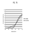
- FIG. 6 is a chart illustrating a difference of a transmission spectrum when the near-infrared cut filter of the example is irradiated with light at a changed incident angle (31 to 60 degrees).
- FIG. 7A is a chart illustrating a difference in transmission spectrum when the near-infrared cut filter of the example is irradiated with light at a changed incident angle (0 degree, 30 degrees).
- FIG. 7B is a chart illustrating a difference in transmission spectrum when the near-infrared cut filter of the example is irradiated with light at a changed incident angle (0 degree, 30 degrees).
- FIG. 7C is a chart illustrating a difference in transmission spectrum when the near-infrared cut filter of the example is irradiated with light while at a changed incident angle (0 degree, 30 degrees).
- FIG. 8 is a schematic diagram illustrating an example of the near-infrared cut filter according to an embodiment of the present invention and an example of an embodiment of a solid-state imaging device according to the present invention using the same.
- FIG. 9 is a schematic diagram illustrating an example of the near-infrared cut filter according to an embodiment of the present invention and an example of an embodiment of the solid-state imaging device according to the present invention using the same.
- FIG. 10 is a schematic diagram illustrating an example of the near-infrared cut filter according to an embodiment of the present invention and an example of an embodiment of the solid-state imaging device according to the present invention using the same.
- a near-infrared cut filter according to the present invention (hereinafter also referred to as an NIR filter) has a stack having a near-infrared absorbing glass substrate and a near-infrared absorbing layer containing a near-infrared absorbing dye and a transparent resin on at least one main surface of the near-infrared absorbing glass substrate, and a dielectric multilayer film formed on at least one main surface of the stack.
- Having the near-infrared absorbing layer on a main surface of the near-infrared absorbing glass substrate means that, as long as it is above the main surface, the near-infrared absorbing layer need not always be in the form in contact with the main surface. That is, another member may exist between the main surface and the near-infrared absorbing layer, and further a space may exist therebetween.
- having the dielectric multilayer film on a main surface of the stack means that the dielectric multilayer film need not always be provided in the form in contact with the main surface.
- This NIR filter has maximum transmittance of 50% or less at an incident angle of 31 to 60 degrees with respect to light with a wavelength of from 775 to 900 nm.
- the maximum transmittance with this wavelength and at this incident angle are preferred to be low for suppressing causes of occurrence of stray light, in-plane unevenness of color or intensity, and the like.
- the maximum transmittance at an incident angle of 31 to 60 degrees with respect to light with a wavelength of from 775 to 900 nm is preferably 30% or less, more preferably 10% or less, furthermore preferably 5% or less, furthermore preferably 3% or less, furthermore preferably 1% or less, furthermore preferably 0.5% or less, furthermore preferably 0.3% or less, particularly preferably 0.2% or less.
- maximum transmittance of 50% or less at an incident angle of 31 to 60 degrees with respect to light with a wavelength of from 775 to 900 nm is 50% or less” (called “rement A”) is construed as including the following cases.
- the “requirement A” is satisfied if a full width at half maximum wavelength including this wavelength is 1 nm or less. Further, even when having a wavelength with which the maximum transmittance exceeds 50% due to the incident angle in the range of 31 to 60 degrees, the “requirement A” is satisfied if a full width at half maximum incident angle including this incident angle is 0.5 degree or less.
- the “requirement A” is satisfied if the maximum transmittance is 50% or less.
- the “requirement A” is satisfied if the maximum transmittance is 50% or less.
- the maximum transmittance is more preferably 50% or less.
- X the maximum transmittance at an incident angle of 31 to 60 degrees with respect to light with a wavelength of from 775 to 900 nm is X % or less
- X is 50, but is given as a value preferred in the order of 30, 10, 5, 3, 1, 0.5, 0.3 and 0.2 as above, specific examples being given below.
- the above “requirement X” is satisfied if the full width at half maximum wavelength including this wavelength is 1 nm or less.
- an average value of transmittance at the incident angle of 0 degree in light with a wavelength of from 450 to 550 nm is preferably 80% or more, more preferably 90% or more.
- an average value of transmittance at the incident angle of 0 degree in light with a wavelength of from 650 to 720 nm is preferably 15% or less.
- an average value of transmittance at the incident angle of 0 degree in light with a wavelength of from 650 to 700 nm is preferably 35% or less, more preferably 30% or less, furthermore preferably 25% or less.
- an average value of transmittance at the incident angle of 0 degree in light with a wavelength of from 690 to 720 nm is more preferably 3% or less.
- the NIR filter according to the present invention has a wavelength ⁇ 0 (NIR) with which transmittance at an incident angle of 0 degree becomes 50% and a wavelength ⁇ 30 (NIR) with which transmittance at an incident angle of 30 degrees becomes 50% in a region of a wavelength longer than 600 nm, and an absolute value of a difference between the wavelengths
- is more preferably 3 nm or less.
- an average of an absolute value of a difference between transmittance at an incident angle of 0 degree and transmittance at an incident angle of 30 degrees is preferably 3% or less, the average value of the absolute value is more preferably 2% or less, in light with a wavelength of from 600 to 750 nm.
- reflectance at an incident angle of 5 degrees with respect to light with a wavelength of from 430 to 600 nm is preferably 2.0% or less, more preferably 1.2% or less, the reflectance being measured excluding reflection of an interface and a surface opposite to the side having the near-infrared absorbing layer of the near-infrared absorbing glass substrate.
- absorptance, transmittance, and reflectance are values measured by using a spectrophotometer.
- transmittance of 70% or more in a specific wavelength region means that transmittance is 70% or more in light of the entire wavelength region
- transmittance of 10% or less means that transmittance is 10% or less in light of the entire wavelength region.
- the measurement of optical properties is, unless described otherwise, performed with respect to light (incident angle of 0 degree) incident from a direction orthogonal to a main surface of a specimen.
- the incident angle is an angle formed by a straight line indicating a direction of incident light with respect to a normal line of a main surface.
- the NIR filter according to the present invention is a near-infrared cut filter with an excellent near-infrared blocking property, in which the near-infrared absorbing glass, the near-infrared absorbing layer containing the near-infrared absorbing dye, and the dielectric multilayer film are effectively used.
- the near-infrared cut filter having a structure, in which maximum transmittance at a relatively large incident angle of 31 to 60 degrees of 50% or less with respect to light of a specific wavelength region (775 to 900 nm) of a near-infrared region, is capable of reducing or preventing occurrence of a phenomenon that an object which did not exist on an original subject appears in a taken image in a solid-state imaging device using the near-infrared cut filter.
- an NIR filter according to a preferred mode of the present invention is a near-infrared cut filter having high average transmittance of the visible range due to that a spectral transmittance curve has a steep inclination in the vicinity of a boundary between the visible range and the near-infrared region, and further having a sufficient near-infrared blocking property without depending on an incident angle of light.
- an average value of transmittance at an incident angle of 0 degree of light in the visible range of wavelength of from 450 to 550 nm is preferably 80% or more, more preferably 85% or more, further preferably 90% or more.
- the NIR cut filter can suppress a change in a spectral transmittance curve of a near-infrared reflection band generated by the dielectric multilayer film with respect to light at an incident angle of 0 to 30 degrees.
- the formula (2) indicates a light blocking property in which an inclination reaching transmittance of 45 to 5% is steeper than an inclination reaching transmittance of 85 to 45% because of having the near-infrared absorbing layer.
- the near-infrared absorbing layer further contains an ultraviolet absorber.
- the NIR filter according to the present invention can achieve an optical property such that an average value of transmittance at an incident angle of 0 degree is 70% or more in light with a wavelength of from 430 to 450 nm, and an average value of transmittance at an incident angle of 0 degree is 5% or less in light with a wavelength of from 350 to 390 nm.
- the near-infrared absorbing layer contains the ultraviolet absorber
- a wavelength with which transmittance at an incident angle of 0 degree becomes 50% is ⁇ 0 (UV) and a wavelength with which transmittance at an incident angle of 30 degrees becomes 50% is ⁇ 30 (UV) in a region where the wavelengths are shorter than 450 nm
- can be made small.
- is preferably 5 nm or less, more preferably 3 nm or less.
- the near-infrared absorbing layer preferably contains an ultraviolet absorber, and an average of absolute values of differences between transmittance at an incident angle of 0 degree and transmittance at an incident angle of 30 degrees in light with a wavelength of from 380 to 430 nm is preferably 8% or less, more preferably 5% or less.
- the NIR filter according to the present invention in which the near-infrared absorbing layer contains an ultraviolet absorber as an optional component has the above-described near-infrared blocking property and is capable of suppressing or preventing occurrence of a phenomenon that an object which did not exist on an original subject appears in a taken image in the solid-state imaging device.
- the spectral transmittance curve has a steep inclination in the vicinity of a boundary between the visible range and an ultraviolet wavelength region (hereinafter referred to as an “ultraviolet region”), and moreover that incident angle dependence of transmittance of light with a wavelength of from 500 nm or less is small, a near-infrared cut filter in which average transmittance of the visible range is made higher can be achieved.
- FIG. 1 to FIG. 3 are cross-sectional views schematically illustrating an example, another example, and still another example of the NIR filter according to the embodiment of the present invention.
- An NIR filter 10 A has a stack L constituted of a near-infrared absorbing glass substrate 11 and a near-infrared absorbing layer 12 , which contains a near-infrared absorbing dye and a transparent resin which are stacked on one main surface of the near-infrared absorbing glass substrate 11 , and a first dielectric multilayer film 13 stacked on the main surface on the near-infrared absorbing glass substrate 11 side of the stack L.
- a modification example of the NIR filter 10 A may be structured such that the stack L has the near-infrared absorbing layer 12 on both main surfaces of the near-infrared absorbing glass substrate 11 , and has a dielectric multilayer film on one or both main surfaces of the stack L. Further, one modification example of the NIR filter 10 A is a structure having a dielectric layer between the near-infrared absorbing glass substrate 11 and the near-infrared absorbing layer 12 .
- An NIR filter 10 B illustrated in FIG. 2 as another example of the NIR filter according to the embodiment has a near-infrared absorbing glass substrate 11 , a near-infrared absorbing layer 12 , which contains a near-infrared absorbing dye and a transparent resin which are stacked on one main surface of the near-infrared absorbing glass substrate 11 , a first dielectric multilayer film 13 stacked on another main surface of the near-infrared absorbing glass substrate 11 , and a second dielectric multilayer film 14 stacked on a main surface of the near-infrared absorbing layer 12 , the main surface being opposite to the near-infrared absorbing glass substrate 11 .
- the NIR filter 10 B has a structure in which a second dielectric multilayer film 14 is stacked on a main surface of the near-infrared absorbing layer 12 of the NIR filter 10 A, the main surface being opposite to the near-infrared absorbing glass substrate 11 .
- An NIR filter 10 C illustrated in FIG. 3 which is still another example of the NIR filter according to the embodiment has a structure similar to the NIR filter 10 B except having a dielectric layer 15 between the near-infrared absorbing glass substrate 11 and the near-infrared absorbing layer 12 in the NIR filter 10 B.
- the NIR filters according to this embodiment can all achieve the maximum transmittance of 50% or less at an incident angle of 31 to 60 degrees with respect to light with a wavelength of from 775 to 900 nm.
- this optical property will be referred to as an optical property of the present invention.
- the structure of the NIR filter 10 B is preferred in view of ability to effectively block near-infrared rays, and the structure of the NIR filter 10 C is more preferred in view of durability or the like.
- the NIR filter according to each embodiment may further include a layer or layers other than the above ones.
- the near-infrared absorbing glass substrate 11 (hereinafter, the near-infrared absorbing glass substrate will simply be referred to as a “glass substrate”) is constituted of a glass having an ability to transmit light in the visible range (450 to 600 nm), and to absorb light in a near infrared region (700 to 1100 nm), for example, a CuO-containing fluorophosphate glass or a CuO-containing phosphate glass (hereinafter, they will also be referred collectively to as a “CuO-containing glass”). Taking a CuO-containing glass substrate constituted of a CuO-containing glass as a typical example, the glass substrate 11 will be explained below.
- the CuO-containing glass substrate has a maximum absorption wavelength ⁇ Gmax in a wavelength of from 775 to 900 nm in an absorption spectrum of light with a wavelength of from 400 to 1100 nm.
- the CuO-containing glass substrate effectively blocks near-infrared light, and thus the CuO content and the thickness may be adjusted so that transmittance T ( ⁇ Gmax ) excluding a surface reflection loss is 50% or less, preferably 30% or less in the maximum absorption wavelength ⁇ Gmax .
- transmittance T ( ⁇ Gmax ) excluding a surface reflection loss is 50% or less, preferably 30% or less in the maximum absorption wavelength ⁇ Gmax .
- T ( ⁇ Gmax ) is 5% or more.
- the glass substrate 11 due to being constituted of the CuO-containing glass, has high transmittance with respect to visible light and has a high blocking property with respect to near-infrared light.
- the “phosphate glass” also includes a siliconphosphate glass in which part of the skeleton of the glass is constituted of SiO 2 .
- Examples of the CuO-containing glass used in the glass substrate 11 include ones having following compositions.
- NF-50E NF-50EX
- NF-50T NF-50TX
- BG-60 product name made by Schott AG
- CD 5000 product name made by HOYA
- the above-described CuO-containing glasses may further contain a metal oxide.
- a metal oxide For example, when one kind or two or more kinds of Fe 2 O 3 , MoO 3 , WO 3 , CeO 2 , Sb 2 O 3 , V 2 O 5 , and the like are contained as the metal oxide, the CuO-containing glasses have an ultraviolet absorbing property.
- the content of the metal oxide is preferably such that at least one kind selected from the group consisting of Fe 2 O 3 , MoO 3 , WO 3 , and CeO 2 is contained by Fe 2 O 3 of from 0.6 to 5 parts by mass, MoO 3 0.5 to 5 parts by mass, WO 3 1 to 6 parts by mass, and CeO 2 2.5 to 6 parts by mass, or two kinds of Fe 2 O 3 and Sb 2 O 3 are contained by Fe 2 O 3 of from 0.6 to 5 parts by mass+Sb 2 O 3 of from 0.1 to 5 parts by mass, or two kinds of V 2 O 5 and CeO 2 are contained by V 2 O 5 of from 0.01 to 0.5 parts by mass+CeO 2 of from 1 to 6 parts by mass, relative to the CuO-containing glass 100 parts by mass.
- the near-infrared blocking performance of the glass substrate 11 may be ones having the optical property of the present invention, that is, the maximum transmittance of 50% or less at an incident angle of 31 to 60 degrees with respect to light with a wavelength of from 775 to 900 nm, as the NIR filters 10 A, 10 B, 10 C obtained by stacking the near-infrared absorbing layer 12 and the first dielectric multilayer film 13 , the second dielectric multilayer film 14 , and the dielectric layer 15 , and the like which will be explained below.
- the glass substrate 11 preferably has absorptance of 75% or more, more preferably 85% or more at an incident angle of 0 degree with respect to light with a wavelength of from 775 to 900 nm in a single state.
- the thickness of the glass substrate 11 is preferably 0.03 to 5 mm from the points of size-reduction and thickness reduction of the device, and prevention of breakage while handled, more preferably 0.05 to 1 mm from the point of weight reduction and strength.
- the optical property of the glass substrate 11 is preferably such that transmittance of light at an incident angle of 0 degree in a wavelength of from 450 to 550 nm is 80% or more in a thickness of 0.03 to 5 mm.
- One material other than the CuO-containing glass for the substrate is a near-infrared absorbing substrate including a near-infrared absorbing dye which absorbs a specific near-infrared and a transparent resin.
- the CuO-containing glass substrate has a characteristic that absorption of light with a wavelength of from 400 to 450 nm is slight, and an absorption ratio of absorption of light with a wavelength of from 400 to 450 nm with respect to light with a wavelength of from 775 to 900 nm is low.
- the CuO-containing glass substrate is useful because significant reduction in transmittance of visible light would not occur when the CuO content is increased so as to sufficiently block light with a wavelength of from 775 to 900 nm by absorption, so as to increase absorptance.
- the NIR filters 10 A, 10 B, 10 C can contribute to, for example, size reduction and thickness reduction of the solid-state imaging device when they are used as a cover to be tightly sealed so as to protect the solid-state image sensing device in the solid-state imaging device.
- ⁇ -ray emitting elements radioactive isotopes
- they may emit ⁇ -rays and cause a transient erroneous operation (software error) in the solid-state image sensing device. Therefore, in the CuO-containing glass constituting the glass substrate 11 in such an application, the content of ⁇ -ray emitting elements is preferred to be as small as possible.
- the contents of U and Th are preferably 20 ppb or less, more preferably 5 ppb or less.
- a surface treatment with a silane coupling agent may be performed on the surface on which the layer is stacked.
- adhesion with the near-infrared absorbing layer 12 may be increased.
- the silane coupling agent for example, the same one as the following one which will be used for the near-infrared absorbing layer 12 can be used.
- the near-infrared absorbing layer 12 is a layer containing a near-infrared absorbing dye (A) and a transparent resin (B), and typically is a layer in which the near-infrared absorbing dye (A) is dispersed evenly through the transparent resin (B).
- the near-infrared absorbing layer 12 is preferred to further contain an ultraviolet absorber (U).
- the near-infrared absorbing layer 12 is illustrated as being constituted of one layer, but is not limited to this structure when the ultraviolet absorber (U) is further contained.
- the near-infrared absorbing layer 12 may be of a structure separately provided with an ultraviolet absorbing layer not-illustrated in FIG. 1 to FIG. 3 . That is, the ultraviolet absorbing layer may contain the ultraviolet absorber (U) and a transparent resin, and may be provided as an independent layer.
- the ultraviolet absorbing layer may be provided on the near-infrared absorbing layer 12 side out of the both main surfaces of the glass substrate 11 , or provided opposite to the near-infrared absorbing layer 12 side.
- the positional relation therebetween is not limited.
- the NIR filters according to the present invention can obtain the same optical property as an optical property of a structure in which the near-infrared absorbing layer 12 further contains the ultraviolet absorber (U).
- the near-infrared absorbing layer 12 contains the near-infrared absorbing dye (A), the transparent resin (B), and moreover the ultraviolet absorber (U), an ultraviolet absorbing layer containing the ultraviolet absorber (U) and a transparent resin may be provided separately.
- the structure in which the ultraviolet absorber (U) is contained in the near-infrared absorbing layer 12 when the NIR filter according to the present invention contains the ultraviolet absorber (U) may be explained below.
- the near-infrared absorbing dye (A) (hereinafter referred to as a dye (A)) is not limited in particular as long as it is a near-infrared absorbing dye having an ability to transmit light in the visible range (wavelength of from 450 to 600 nm), and to absorb light in the near-infrared region (wavelength of from 700 to 1100 nm).
- the dye in the present invention may be a pigment, that is, may be in a state of being an aggregate of molecules.
- the near-infrared absorbing dye may be referred to as a “NIR absorbing dye” as necessary.
- the dye (A) is preferably a material having the maximum absorption wavelength ⁇ max at a wavelength of from 650 to 750 nm, further preferably a material having the ⁇ max at a wavelength of from 680 to 720 nm.
- the near-infrared absorbing layer containing the dye (A) has a high freedom in selection of type and content of the material which can narrow the absorption wavelength bandwidth, as compared to the near-infrared absorbing glass.
- adjusting the transmittance T ( ⁇ max ) at its maximum absorption wavelength ⁇ max to be lower than the transmittance T ( ⁇ Gmax ) in the maximum absorption wavelength ⁇ Gmax of the near-infrared absorbing glass substrate enables the near-infrared absorbing layer to achieve a steep light blocking property in the vicinity of the ⁇ max while preventing decrease in transmittance of the visible wavelength region.
- the maximum absorption wavelength in the near-infrared absorbing layer containing the dye (A) having the maximum absorption wavelength ⁇ max matches the maximum absorption wavelength ⁇ max of the dye (A).
- the dye (A) and the content thereof in the transparent resin (B) are adjusted so that its absorption of light with a wavelength of from about 550 to 600 nm with high visibility is small and maintains high transmittance, the transmittance with respect to light with a wavelength of from about 600 to 650 nm with gradually decreasing visibility decreases to about 40 to 60%, and transmittance with respect to light with a wavelength of from about 650 to 700 nm with from a level of low visibility to a level of almost no visibility decreases to 5% or less.
- the dye (A) and the content thereof are adjusted so that the transmittance T ( ⁇ max ) at the ⁇ max in the near-infrared absorbing layer becomes 5% or less.
- the absorption wavelength band which yields low transmittance with near-infrared light more than or equal to about 700 nm as a result of adjusting the dye (A) so that the transmittance with respect to light with a wavelength of from 550 to 700 nm is in the above preferred range, is preferred to be wider.
- the absorption wavelength bandwidth in which the transmittance becomes 20% or less in the vicinity of the ⁇ max is preferably 30 nm or more, more preferably 40 nm or more.
- the near-infrared absorbing layer has the above-described absorption wavelength bandwidth, it is possible to increase the effect to block transmitted light in the near-infrared region, which cannot be blocked sufficiently by absorption by the near-infrared absorbing glass substrate and the near-infrared absorbing layer, by using a dielectric multilayer film with a near-infrared reflective property, which will be described later.
- the NIR filter based on this design can prevent incident angle dependence of the dielectric multilayer film affecting the spectral transmittance curve particularly in a near-infrared absorbing region.
- the dye (A) is preferably one exhibiting the maximum absorption wavelength in the wavelength of from 650 to 750 nm in the absorption spectrum of light with a wavelength of from 400 to 850 nm measured by using a resin film obtained by dispersing the dye (A) through the transparent resin (B).
- the near-infrared absorbing dye having this absorbing property is called a dye (A 1 )
- the maximum absorption wavelength in this absorption spectrum is called ⁇ max of the dye (A1).
- the absorption spectrum of the dye (A1) has an absorption peak having an apex of absorption at a wavelength ⁇ max (hereinafter referred to as an “absorption peak of ⁇ max ”).
- the absorption spectrum of the dye (A1) in addition to having the ⁇ max in the wavelength of from 650 to 750 nm, preferably, absorption of visible light is small, and the inclination on the visible light side of the absorption peak of ⁇ max is steep. Moreover, the absorption peak of the ⁇ max preferably has a gradual inclination on the long wavelength side.
- Examples of the dye (A1) include a cyanine-based compound, a phthalocyanine-based compound, a naphthalocyanine-based compound, a dithiol metal complex-based compound, a diimonium-based compound, a polymethine-based compound, a phthalide compound, a naphthoquinone-based compound, an anthraquinone-based compound, an indophenol-based compound, a squarylium-based compound, and the like.
- the squarylium-based compound, the cyanine-based compound, and the phthalocyanine-based compound are more preferred, and the squarylium-based compound is particularly preferred.
- the dye (A1) constituted of the squarylium-based compound is preferred because its absorption of visible light is small in the absorption spectrum, the absorption peak of the ⁇ max has a steep inclination on the visible light side, and storage stability and stability with respect to light are high.
- the dye (A1) constituted of the cyanine-based compound is preferred because its absorption of visible light is small in the absorption spectrum, and absorptance of light on the long wavelength side is high in a wavelength region in the vicinity of the ⁇ max .
- the cyanine-based compound is of low costs, and is known to secure long-term stability by forming salt.
- the dye (A1) constituted of the phthalocyanine-based compound is preferred because of its excellence in heat resistance and weather resistance.
- One example of the dye (A1) which is the squarylium-based compound is, specifically, at least one kind selected from squarylium-based compounds represented by a formula (F1)
- a chemical compound represented by the formula (F1) will also be called a chemical compound (F1)
- the chemical compound (F1) is a squarylium-based compound having a structure in which benzene rings are bonded to the left and right sides of a squarylium skeleton, nitrogen atoms are further bonded to fourth positions of the benzene rings, and saturated heterocycles including the nitrogen atoms are formed, and is a chemical compound having a light absorbing property as the dye (A1).
- substituents of the benzene rings can be adjusted appropriately in the following ranges according to other required properties such as increasing solubility to a solvent used when the near-infrared absorbing layer is formed (hereinafter may be referred to as a “host solvent”) or to the transparent resin (B), or the like.
- R 5 and R 6 independently represents a hydrogen atom, a halogen atom, a hydroxyl group, an alkyl group or an alkoxy group having 1 to 6 carbon atoms, an acyloxy group having 1 to 10 carbon atoms, or —NR 7 R 8 (R 7 and R 8 each independently represent a hydrogen atom, an alkyl group having 1 to 20 carbon atoms, or —C( ⁇ O)—R 9 (R 9 is a hydrogen atom, an alkyl group having 1 to 20 carbon atoms or an aryl group having 6 to 11 carbon atoms which may have a substituent, or an alaryl group having 7 to 18 carbon atoms which may have a substituent and may have an oxygen atom between carbon atoms)).
- At least one group of R 1 and R 2 , R 2 and R 5 , and R 1 and R 3 couple together to form a heterocycle A, a heterocycle B, and a heterocycle C having 5 or 6 members including a nitrogen atom.
- R 1 and R 2 when the heterocycle A is formed represent, as a bivalent group -Q- in which they are bonded, an alkylene group or an alkyleneoxy group, in which hydrogen atoms may be substituted by an alkyl group having 1 to 6 carbon atoms, an awl group having 6 to 10 carbon atoms, or an acyloxy group having 1 to 10 carbon atoms which may have a substituent.
- R 2 and R 5 when the heterocycle B is formed and R 1 and R 3 when the heterocycle C is formed represent, each as a bivalent group —X 1 —Y 1 — and —X 2 —Y 2 — in which they are bonded (the side bonded to nitrogen is X 1 or X 2 ), a group in which each of X 1 and X 2 is represented by following formulae (1x) or (2x) and a group in which each of Y 1 and Y 2 is represented by one selected from following formulae (1y) to (5y).
- Y 1 and Y 2 may each be a single bond.
- Zs each independently represent a hydrogen atom, a hydroxyl group, an alkyl group or an alkoxy group having 1 to 6 carbon atoms, or an alkoxy group, or —NR 28 R 29 (R 28 and R 29 each independently represent a hydrogen atom or an alkyl group having 1 to 20 carbon atoms).
- R 21 to R 26 each independently represent a hydrogen atom, an alkyl group having 1 to 6 carbon atoms or an aryl group having 6 to 10 carbon atoms
- R 27 represents an alkyl group having 1 to 6 carbon atoms or an aryl group having 6 to 10 carbon atoms.
- R 7 , R 8 , R 9 , R 4 , R 6 , R 21 to R 27 , R 1 to R 3 when the heterocycles are not formed, and R 5 may be bonded to another one of them to form a five-membered ring or a six-membered ring.
- R 21 and R 26 , and R 21 and R 27 may be bonded directly.
- R 1 and R 2 when the heterocycles are not formed each independently represent a hydrogen atom, an alkyl group or an allyl group having 1 to 6 carbon atoms which may have a substituent, or an aryl group or an alaryl group having 6 to 11 carbon atoms.
- R 3 and R 5 when the heterocycles are not formed each independently represent a hydrogen atom, a halogen atom, or an alkyl group or an alkoxy group having 1 to 6 carbon atoms.
- the heterocycle A may simply be referred to as a ring A.
- R 4 and R 6 each independently represent the above atoms or groups.
- the halogen atom include a fluorine atom, a chlorine atom, a bromine atom, or the like.
- the alkyl group may be any of linear chain, branched chain, and cyclic.
- R 4 and R 6 are preferably of a combination in which one of them is a hydrogen atom and the other is —NR 7 R 8 .
- —NR 7 R 8 may be introduced into either of R 4 and R 6 .
- —NR 7 R 8 is preferably introduced into R 4 .
- the chemical compound has only the ring C, or only the ring A and the ring C, —NR 7 R 8 is preferably introduced into R 6 .
- R 9 is preferably an alkyl group having 1 to 20 carbon atoms which may have a substituent, an aryl group having 6 to 10 carbon atoms which may have a substituent, or an alaryl group having 7 to 18 carbon atoms which may have a substituent and may have an oxygen atom between carbon atoms.
- substituents examples include a halogen atom such as a fluorine atom, a hydroxyl group, a carboxy group, a sulfo group, a cyano group, an alkyl group having 1 to 6 carbon atoms, a fluoroalkyl group having 1 to 6 carbon atoms, an alkoxy group having 1 to 6 carbon atoms, an acyloxy group having 1 to 6 carbon atoms, and the like.
- halogen atom such as a fluorine atom, a hydroxyl group, a carboxy group, a sulfo group, a cyano group, an alkyl group having 1 to 6 carbon atoms, a fluoroalkyl group having 1 to 6 carbon atoms, an alkoxy group having 1 to 6 carbon atoms, an acyloxy group having 1 to 6 carbon atoms, and the like.
- R 9 is preferably a group selected from a linear, branched, or cyclic alkyl group having 1 to 17 carbon atoms which may be substituted by a fluorine atom, a phenyl group which may be substituted by a fluoroalkyl group having 1 to 6 carbon atoms, and/or an alkoxy group having 1 to 6 carbon atoms, and an alaryl group having 7 to 18 carbon atoms which may have an oxygen atom between carbon atoms and has, on its terminal, an alkyl group having 1 to 6 carbon atoms which may be substituted by a fluorine atom and/or a phenyl group which may be substituted by an alkoxy group having 1 to 6 carbon atoms.
- a group can be preferably used which is a hydrocarbon group having 5 to 25 carbon atoms and having at least one or more branches, in which one or more hydrogen atoms may be independently substituted by a halogen atom, a hydroxyl group, a carboxy group, a sulfo group, or a cyano group, and which may include an unsaturated bond, an oxygen atom, or a saturated or unsaturated ring structure between carbon atoms.
- R 9 include groups represented by formulae (1a), (1b), (2a) to (2e), (3a) to (3e).
- R 1 and R 2 when the rings are not formed each independently represent a hydrogen atom, an alkyl group or allyl group having 1 to 6 carbon atoms which may have a substituent, or an aryl group or alaryl group having 6 to 11 carbon atoms.
- the alkyl group may be any of linear chain, branched chain, and cyclic. Examples of the substituent include a hydroxyl group, an alkoxy group having 1 to 3 carbon atoms, and an acyloxy group having 1 to 3 carbon atoms.
- R 3 and R 5 when the rings are not formed each independently represent a hydrogen atom, a halogen atom, or an alkyl group or alkoxy group having 1 to 6 carbon atoms.
- R 1 , R 2 , R 3 , R 5 from the viewpoint of solubility to the host solvent or the transparent resin (B), an alkyl group having 1 to 3 carbon atoms is preferred, and a methyl group, an ethyl group, or a 2-propyl group is particularly preferred.
- R 1 to R 6 which the benzene rings bonded to the left and right sides of a squarylium skeleton have may be different on the left and right sides, but is preferred to be the same on the left and right sides.
- the chemical compound (F1) contains a chemical compound (F1-1) expressed by a formula (F1-1) having a resonance structure of the structure expressed by the formula (F1)
- Examples of the chemical compound (F1) more specifically include the chemical compound expressed by a formula (F11) having only the ring B as a ring structure, the chemical compound expressed by a formula (F12) having only the ring A as a ring structure, and the chemical compound expressed by a formula (F13) having two of the ring B and the ring C as ring structures.
- the chemical compound represented by the formula (F11) is the same chemical compound as the chemical compound having only the ring C as a ring structure in the chemical compound (F1) with R 6 being —NR 7 R 8 .
- the chemical compound expressed by the formula (F11) and the chemical compound expressed by the formula (F13) are chemical compounds described in the U.S. Pat. No. 5,543,086.
- X 1 an ethylene group in which the hydrogen atom may be substituted by an alkyl group having 1 to 6 carbon atoms or an aryl group having 6 to 10 carbon atoms expressed in the above (2x) is preferred.
- an alkyl group having 1 to 3 carbon atoms is preferred, and a methyl group is more preferred.
- Examples of X 1 specifically include —(CH 2 ) 2 —, —CH 2 —C(CH 3 ) 2 —, —CH(CH 3 )—C(CH 3 ) 2 —, —C(CH 3 ) 2 —C(CH 3 ) 2 —, and the like.
- —NR 7 R 8 in chemical compound (F11) —NH—C( ⁇ O)—CH 3 , —NH—C( ⁇ O)—C 6 H 13 , —NH—C( ⁇ O)—C 6 H 5 , —NH—C( ⁇ O)—CH(C 2 H 5 )—C 4 H 9 , —NH—C( ⁇ O)—C(CH 3 ) 2 —C 2 H 5 , —NH—C( ⁇ O)—C(CH 3 ) 2 —C 3 H 7 , —NH—C( ⁇ O)—C(CH 3 ) 2 —(CH 2 ) 3 —O—C 6 H 3 (CH 3 ) 2 , or the like is preferred.
- Examples of the chemical compound (F11) include chemical compounds expressed by formula (F11-1), formula (11-2), formula (F11-3), formula (F11-4), formula (F11-5), formula (F11-6), formula (F11-7), and the like. Among them, due to high solubility to the host solvent and the transparent resin (B), the chemical compound (F11-2), the chemical compound (F11-3), the chemical compound (F11-4), the chemical compound (F11-5), and the chemical compound (F11-6) are more preferred.
- Q is an alkylene group having 4 or 5 carbon atoms or an alkyleneoxy group having 3 or 4 carbon atoms, in which hydrogen atoms may be substituted by an alkyl group having 1 to 6 carbon atoms, an aryl group having 6 to 10 carbon atoms, or an acyloxy group having 1 to 10 carbon atoms which may have a substituent.
- the position of oxygen atom in the case of the alkyleneoxy group is preferably other than where it is adjacent to N.
- a butylene group which may be substituted by an alkyl group having 1 to 3 carbon atoms, particularly a methyl group is preferred.
- the ⁇ max of the chemical compound (F12) is on the relatively long wavelength side in the above-described wavelength region, using the chemical compound (F12) can widen the transmission region of the visible wavelength band.
- the chemical compound (F12) include chemical compounds represented by formula (F12-1), formula (F12-2), formula (F12-3), and the like.
- X 1 and X 2 are independently preferably an ethylene group in which the hydrogen atom expressed by the above (2x) may be substituted by an alkyl group having 1 to 6 carbon atoms or an aryl group having 6 to 10 carbon atoms.
- the substituent is preferably an alkyl group having 1 to 3 carbon atoms, more preferably a methyl group.
- X 1 and X 2 may be, specifically, —(CH 2 ) 2 —, —CH 2 —C(CH 3 ) 2 —, —CH(CH 3 )—C(CH 3 ) 2 —, —C(CH 3 ) 2 —C(CH 3 ) 2 —, and the like.
- Y 1 and Y 2 may be, independently, —CH 2 —, —C(CH 3 ) 2 —, —CH(C 6 H 5 )—, —CH((CH 2 ) m CH 3 )— (m is 0 to 5), and the like.
- —NR 7 R 8 is preferably —NH—C( ⁇ O)—C m H 2m+1 (m is 1 to 20, and C m H 2m+1 may be any of linear chain, branched chain, and cyclic), —NH—C( ⁇ O)-Ph-R 10 (-Ph- represents a phenylene group, and R 10 represents a hydrogen atom, an alkyl group having 1 to 3 carbon atoms, an alkoxy group having 1 to 3 carbon atoms, or a perfluoroalkyl group having 1 to 3 carbon atoms), or the like.
- Examples of the chemical compound (F13) include chemical compounds expressed by a following formula (F13-1), formula (F13-2), and the like.
- a dye (A1) it is also possible to use a squarylium-based compound represented by a formula (F6).
- the formula (F6) expresses a chemical compound in which none of the ring A, the ring B, and the ring C is formed in the formula (F1) (where R 1 to R 6 are as follows).
- R 1 and R 2 each independently represent a hydrogen atom, an alkyl group or an allyl group having 1 to 12 carbon atoms which may have a substituent, or an aryl group or an alaryl group having 6 to 11 carbon atoms.
- R 3 and R 5 each independently represent a hydrogen atom, a halogen atom, or an alkyl group or an alkoxy group having 1 to 6 carbon atoms.
- R 4 and R 6 each independently represent a hydrogen atom, a halogen atom, a hydroxyl group, or an alkyl group or an alkoxy group having 1 to 6 carbon atoms, an acyloxy group having 1 to 10 carbon atoms, or —NR 7 R 8 (R 7 and R 8 each independently represent a hydrogen atom, an alkyl group having 1 to 20 carbon atoms, or —C( ⁇ O)—R 9 (R 9 is a hydrogen atom, an alkyl group having 1 to 20 carbon atoms or an aryl group having 6 to 11 carbon atoms which may have a substituent, or an alaryl group having 7 to 18 carbon atoms which may have a substituent and may have an oxygen atom between carbon atoms)).
- the chemical compound (F6) include chemical compounds expressed by a formula (F6-1), formula (F6-2), and the like.
- a squarylium-based chemical compound expressed by a formula (F7) can also be used.
- the above-described chemical compound (F1) such as the chemical compound (F11), the chemical compound (F12), or the chemical compound (F13), as well as the chemical compound (F6) and the chemical compound (F7) can be produced by a conventionally known method.
- the chemical compound (F11) such as the chemical compound (F11-1) can be produced by a method described in, for example, U.S. Pat. No. 5,543,086.
- the chemical compound (F12) can be produced by a method described in, for example, J. Org. Chem. 2005, 70 (13), 5164-5173.
- the chemical compound (F12-1), the chemical compound (F12-2), and the like can be produced according to, for example, a synthetic pathway expressed in a reaction formula (F3).
- a reaction formula (F3) an amino group of 1-methyl-2-iodine-4-amino benzene is brought into reaction with a carboxylic acid chloride having a desired substituent R 9 to form an amide. Then, it is brought into reaction with pyrrolidine and further into reaction with 3,4-dihydroxy-3-cyclobutene-1,2-dione (hereinafter referred to as squaric acid), thereby obtaining the chemical compound (F12-1), the chemical compound (F12-2), or the like.
- squaric acid 3,4-dihydroxy-3-cyclobutene-1,2-dione
- R 9 represents -Ph or —(CH 2 ) 5 —CH 3 .
- -Ph represents a phenyl group.
- Et represents an ethyl group, and THF represents a tetrahydrofuran.
- the chemical compound (F13-1), the chemical compound (F13-2), and the like can be produced according to, for example, a synthetic pathway expressed in a reaction formula (F4).
- reaction formula (F4) first, 8-hydroxyjulolidine is brought into reaction with trifluoromethanesulfonic acid anhydride (Tf 2 O) to make 8-julolidine trifluoromethanesulfonate, and then it is brought into reaction with benzylamine (BnNH 2 ) to obtain 8-benzylamino julolidine, and then it is further reduced to produce 8-amino julolidine.
- Tf 2 O trifluoromethanesulfonic acid anhydride
- BnNH 2 benzylamine
- an amino group of the 8-amino julolidine is brought into reaction with a carboxylic acid chloride having a desired substituent R 9 (—(CH 2 ) 6 —CH 3 in the case of the chemical compound (F13-1), or —CH(CH(CH 3 )—CH 2 —C(CH 3 ) 3 )—(CH 2 ) 2 —CH(CH 3 )—CH 2 —C(CH 3 ) 3 in the case of the chemical compound (F13-2)), thereby obtaining a chemical compound having —NH—C( ⁇ O)R 9 at an eighth position of the julolidine.
- 2 moles of this chemical compound is brought into reaction with one mole of squaric acid, thereby obtaining the chemical compound (F13-1), the chemical compound (F13-2), or the like.
- Me represents a methyl group
- TEA represents triethylamine
- Ac represents an acetyl group
- BINAP represents (2,2′-bis(diphenylphosphino)-1,1′-binaphthyl)
- NaOtBu represents sodium-t-butoxide.
- the dye (A1) which is a squarylium-based compound
- a commercial product may be used.
- the commercial product include S2098, S2084 (product names, made by FEW Chemicals), and the like.
- the dye (A1) which is a cyanine-based compound may be, specifically, at least one selected from cyanine-based compounds expressed by a formula (F5).
- R 11 each independently represents an alkyl group, alkoxy group or alkyl sulfone group having 1 to 20 carbon atoms, or an anion species thereof.
- R 12 and R 13 each independently represent a hydrogen atom or an alkyl group having 1 to 20 carbon atoms.
- Z represents a PF 6 , ClO 4 , R f —SO 2 , (R f —SO 2 ) 2 —N (R f represents an alkyl group having 1 to 8 carbon atoms in which at least one hydrogen atom is substituted by a fluorine atom), or BF 4 .
- R 14 , R 15 , R 16 and R 17 each independently represent a hydrogen atom, a halogen atom, or an alkyl group having 1 to 6 carbon atoms.
- n represents an integer of 1 to 6.
- R 11 in the chemical compound (F5) is preferably an alkyl group having 1 to 20 carbon atoms
- R 12 and R 13 are each independently preferably a hydrogen atom or an alkyl group having 1 to 6 carbon atoms.
- R 14 , R 15 , R 16 and R 17 are each independently preferably a hydrogen atom, and the number of n is preferably 1 to 4.
- the structure of the left and right sides across n repetitive units may be different, but is preferably the same structure.
- the chemical compound (F5) more specifically, a chemical compound expressed by a formula (F51), a chemical compound expressed by a formula (F52), and the like are exemplified.
- the anion represented by Z ⁇ is similar to Z ⁇ in (F5).
- the dye (A1) which is a cyanine-based compound a commercial product may be used.
- the commercial product include ADS680HO (product name, made by American Dye), S0830 (product name, made by FEW Chemicals), S2137 (product name, made by FEW Chemicals), and the like.
- examples of a phthalocyanine-based chemical compound usable as the dye (A1) include commercial products such as FB22 (product name, made by Yamada Chemical Co, Ltd.), TXEX720 (product name, made by Nippon Shokubai Co, Ltd.), PC142c (product name, made by Yamada Chemical Co., Ltd.), and the like.
- ⁇ max of chemical compounds used as the dye (A1) exemplified above are presented in Table 1 together with the types of the transparent resins (B) used at the time of measurement.
- the B-OKP2 and Vylon (registered trademark) 103 used above as the transparent resin (B) are polyester resins, SP3810 is a polycarbonate resin, and EA-F5003 is an acrylic resin, details of which are as will be described later.
- the dye (A1) one kind selected from a plurality of chemical compounds having a light absorbing property as the dye (A1) may be used solely, or two kinds or more selected therefrom may be used together.
- the dye (A) preferably contains one kind or two or more kinds of the dye (A1). Note that the dye (A) may contain any NIR absorbing dye as necessary other than the dye (A1).
- the NIR absorbing dyes When a plurality of NIR absorbing dyes are used as the dye (A), it is preferred to use the NIR absorbing dyes in combination so that the maximum absorption wavelength appears in the wavelength of from 650 to 750 nm in an absorption spectrum of light with a wavelength of from 400 to 850 nm measured with respect to a resin film produced by dispersing the dyes in the transparent resin (B). Moreover, it is preferred to use the NIR absorbing dyes in combination so that absorption of visible light is small, an inclination on the visible light side of the absorption peak of ⁇ max is steep, and the inclination is gradual on the long wavelength side in this absorption spectrum.
- the ultraviolet absorber (U) (hereinafter may also be referred to as an absorber (U)) is a chemical compound absorbing light with a wavelength of 430 nm or less.
- an absorber (U1) a chemical compound satisfying requirements (iv-1) and (iv-2) is preferred.
- the absorber has at least one maximum absorption wavelength at a wavelength of 415 nm or less in a light absorption spectrum of a wavelength of from 350 to 800 nm measured after dissolved in dichloromethane, and the maximum absorption wavelength ⁇ max (UV) on the longest-wavelength side in the maximum absorption in light with a wavelength of 415 nm or less is in a wavelength of from 360 to 415 nm.
- the maximum absorption wavelength of the absorber (U) satisfying (iv-1) does not change largely in the transparent resin. That is, the absorber (U) satisfying (iv-1) is preferred because the maximum absorption wavelength ⁇ max-P (UV) in an in-resin absorption spectrum exists approximately within a wavelength of from 360 to 415 nm when this absorber (U) is dissolved or dispersed in the transparent resin.
- the absorber (U) satisfying (iv-2) exhibits excellent steepness when contained in the transparent resin. That is, also when the absorber (U) is dissolved or dispersed in the transparent resin, the absorber (U) satisfying (iv-2) is preferred because the difference ( ⁇ P90 - ⁇ P50 ) between the wavelength ⁇ P50 with which transmittance becomes 50% at a longer wavelength than the maximum absorption wavelength ⁇ max ⁇ P (UV) and the wavelength ⁇ P90 with which the transmittance becomes 90% is approximately 14 nm or less, thereby exhibiting steepness equal to that in dichloromethane.
- ⁇ P90 - ⁇ P50 when the absorber (U) is dissolved or dispersed in the transparent resin is preferably 13 nm or less, more preferably 12 nm or less.
- a wavelength ⁇ 0 (UV) and a wavelength ⁇ 30 (UV) of the NIR filter in the embodiment obtained as the near-infrared absorbing layer 12 by dissolving or dispersing it into the transparent resin can both be made to exist in a shorter region than the wavelength of 450 nm, preferably, at a wavelength of from 400 to 425 nm.
- the absorber (U) satisfying (iv-2) is used, in the NIR filter in the embodiment obtained as the near-infrared absorbing layer 12 by dissolving or dispersing it into the transparent resin, the difference between the wavelength with which transmittance becomes 50% on the long-wavelength side of the maximum absorption wavelength by the absorber (U) and the wavelength with which the transmittance becomes 90% can be made small. That is, in this wavelength region, a change in the spectral transmittance curve can be made steep.
- the absorber (U1) satisfying (iv-1) and (iv-2) is used, it is easy to make the wavelength ⁇ 0 (UV) and the wavelength ⁇ 30 (UV) exist in a region shorter than the wavelength 450 nm in the NIR filter of the embodiment, preferably a wavelength of from 400 to 425 nm, and a steep change of the spectral transmittance curve in a shorter region than the wavelength 450 nm can be obtained easily.
- the absorption spectrum of light with a wavelength of from 350 to 800 nm measured when the absorber (U) is dissolved in dichloromethane will also be referred to as an “absorption spectrum of the absorber (U)”.
- the maximum absorption wavelength ⁇ max (UV) in the absorption spectrum of the absorber (U) will be referred to as the “ ⁇ max (UV) of the absorber (U)”.
- the spectral transmittance curve measured when the absorber (U) is dissolved in dichloromethane will be referred to as a “spectral transmittance curve of the absorber (U)”.
- the wavelength with which the transmittance becomes 90% at a longer wavelength than the ⁇ max (UV) of the absorber (U) will be referred to as “ ⁇ L90 ”
- the wavelength with which the transmittance becomes 50% at a longer wavelength than the ⁇ max (UV) of the absorber (U) will be referred to as “ ⁇ L50 ”.
- the absorption spectrum of light with a wavelength of from 350 to 800 nm measured in an absorption layer produced by dissolving the absorber (U) in the transparent resin will also be referred to as an “in-resin absorption spectrum of the absorber (U)”.
- the maximum absorption wavelength ⁇ max ⁇ p (UV) in the in-resin absorption spectrum of the absorber (U) will be referred to as the ⁇ max ⁇ p (UV) of the absorber (U)′′.
- a spectral transmittance curve measured in an absorption layer produced by dissolving the absorber (U) in the transparent resin will be referred to as an “in-resin spectral transmittance curve of the absorber (U)”.
- the wavelength with which the transmittance becomes 90% at a longer wavelength than the ⁇ max (UV) of the absorber (U) will be referred to as “ ⁇ P90 ”
- the wavelength with which the transmittance becomes 50% at a longer wavelength than the ⁇ max ⁇ P (UV) of the absorber (U) will be referred to as “ ⁇ P50 ”.
- the wavelength ⁇ max (UV) of the absorber (U) is preferably at a wavelength of from 365 to 415 nm, more preferably at a wavelength of from 370 to 410 nm.
- the wavelength ⁇ max (UV) of the absorber (U) being in this region makes it easy to obtain the above-described effect, namely, the steep change of the spectral transmittance curve at a wavelength of from 400 to 425 nm.
- the difference ( ⁇ L90 - ⁇ L50 ) between ⁇ L90 and ⁇ L50 of the absorber (U) is preferably 12 nm or less, more preferably 11 nm or less, furthermore preferably 9 nm or less.
- the ⁇ L90 - ⁇ L50 being in this region makes it easy to obtain the above-described effect.
- the absorber (U1) which satisfies (iv-1) and (iv-2) include dyes of oxazole-based, merocyanine-based, cyanine-based, naphthalimide-based, oxadiazole-based, oxazine-based, oxazolidine-based, naphthalic acid-based, styryl-based, anthracene-based, cyclic carbonyl-based, triazole-based, and the like.
- Examples of commercial products include, as the oxazole-based dye, Uvitex (registered trademark) OB (product name made by Ciba), Hakkol (registered trademark) RF-K (product name made by Showa Chemical Industry Co., Ltd.), Nikkafluor EFS, Nikkafluor SB-conc (product names both being made by Nippon Chemical Industrial CO., LTD.), and the like.
- Examples of the merocyanine-based dye include S0511 (product name made by FEW Chemicals), and the like.
- Examples of the cyanine-based dye include SMP370, SMP416 (both being product names made by Hayashibara Co., Ltd.), and the like.
- Examples of the naphthalimide-based dye include Lumogen (registered trademark) F violet 570 (product name made by BASF), and the like.
- Examples of the absorber (U1) include dyes expressed by a formula (N). Note that in this specification, unless otherwise particularly mentioned, the dye expressed by a formula (N) will be described as a dye (N). A dye expressed by another formula is also described similarly. Further, a group expressed by a formula (In) will be described as a group (1n). Any group expressed by another formula will be described similarly.
- R 18 in the formula (N) may each independently represent a hydrocarbon group having 1 to 20 carbon atoms which may contain a saturated or unsaturated ring structure, and may have a branch. Specific examples include an alkyl group, an alkenyl group, a saturated cyclic hydrocarbon group, an awl group, and an alaryl group of linear chain or branched chain, and the like. Further, in the formula (N), R 19 are each independently a cyano group or a group expressed by a formula (n). —COOR 30 (n) In the formula (n), R 30 represents a hydrocarbon group having 1 to 20 carbon atoms which may contain a saturated or unsaturated ring structure, and may have a branch. Specific examples include an alkyl group, an alkenyl group, a saturated cyclic hydrocarbon group, an awl group, and an alaryl group of linear chain or branched chain, and the like.
- R 18 in the dye (N) are preferably, among others, a group expressed by formulae (1n) to (4n). Further, R 19 in the dye (N) are preferably, among others, a group expressed by a formula (5n).
- dyes (N-1) to (N-4) of structures presented in Table 2 can be exemplified.
- specific structures of R 18 and R 19 in Table 2 correspond to formulae (1n) to (5n).
- Corresponding dye abbreviations are also presented in Table 2. Note that in the dyes (N-1) to (N-4), two R 18 present are the same, and R 19 are the same as well.
- the dyes of oxazole-based and merocyanine-based are preferred, and examples of commercial products thereof include Uvitex (registered trademark) OB, Haldol (registered trademark) RF-K, and S0511.
- absorber (U1) merocyanine-based dyes expressed by a formula (M) are particularly preferred.
- Y represents an oxygen atom or a methylene group substituted by Q 6 and Q 7 .
- Q 6 and Q 7 each independently represent a hydrogen atom, a halogen atom, or an alkyl group or an alkoxy group having 1 to 10 carbon atoms.
- Q 6 and Q 7 are preferably each independently a hydrogen atom or an alkyl group or an alkoxy group having 1 to 10 carbon atoms, and more preferably are both a hydrogen atom or at least one of them is a hydrogen atom and the other is an alkyl group having 1 to 4 carbon atoms.
- Q 6 and Q 7 are both a hydrogen atom.
- Q 1 represents a monovalent hydrocarbon group having 1 to 12 carbon atoms which may have a substituent.
- the monovalent hydrocarbon group is preferably an alkyl group having 1 to 12 carbon atoms in which part of hydrogen atoms may be substituted by an aliphatic ring, an aromatic ring or an alkenyl group, a cycloalkyl group having 3 to 8 carbon atoms in which part of hydrogen atoms may be substituted by an aromatic ring, an alkyl group or an alkenyl group, and an aryl group having 6 to 12 carbon atoms in which part of hydrogen atoms may be substituted by an aliphatic ring, an alkyl group or an alkenyl group.
- this alkyl group may be of either linear chain or branched chain, and a number of carbon atoms thereof is more preferably 1 to 6.
- alkyl group having 1 to 12 carbon atoms in which part of hydrogen atoms are substituted by an aliphatic ring, an aromatic ring or an alkenyl group an alkyl group having 1 to 4 carbon atoms having a cycloalkyl group having 3 to 6 carbon atoms and an alkyl group having 1 to 4 carbon atoms which is substituted by a phenyl group are more preferred, and an alkyl group having 1 or 2 carbon atoms which is substituted by a phenyl group is particularly preferred.
- the alkyl group substituted by an alkenyl group means one which is an alkenyl group in its entirety but has no unsaturated bond between a first position and a second position, for example, an allyl group or 3-butenyl group, or the like.
- the hydrocarbon group having a substituent a hydrocarbon group having one or more of an alkoxy group, an acyl group, an acyloxy group, a cyano group, a dialkylamino group or a chlorine atom is preferred.
- the number of carbon atoms of these alkoxy group, acyl group, acyloxy group and dialkylamino group is preferably 1 to 6.
- Preferred Q 1 is an alkyl group having 1 to 6 carbon atoms in which part of hydrogen atoms may be substituted by a cycloalkyl group or a phenyl group.
- Particularly preferred Q 1 is an alkyl group having 1 to 6 carbon atoms, and specific example include a methyl group, an ethyl group, a propyl group, an isopropyl group, a butyl group, an isobutyl group, a t-butyl group, and the like.
- Q 2 to Q 5 each independently represent a hydrogen atom, a halogen atom, or an alkyl group or an alkoxy group having 1 to 10 carbon atoms.
- the number of carbon atoms of the alkyl group and the alkoxy group is preferably 1 to 6, more preferably 1 to 4.
- At least one of Q 2 and Q 3 is preferably an alkyl group, and both of them are more preferably an alkyl group.
- a hydrogen atom is more preferred.
- Both Q 2 and Q 3 are particularly preferably an alkyl group having 1 to 6 carbon atoms.
- At least one of Q 4 and Q 5 is preferably a hydrogen atom, and more preferably both of them are a hydrogen atom.
- alkyl group having 1 to 6 carbon atoms is preferred.
- Z represents any of bivalent groups expressed by formulae (Z1) to (Z5).
- Q 8 and Q 9 each independently represent a monovalent hydrocarbon group having 1 to 12 carbon atoms which may have a substituent.
- Q 8 and Q 9 may be different groups but preferably are the same groups.
- this alkyl group may be of either linear chain or branched chain, and a number of carbon atoms thereof is more preferably 1 to 6.
- a number of carbon atoms thereof is more preferably 1 to 6.
- an alkyl group having 1 to 12 carbon atoms in which part of hydrogen atoms are substituted by an aliphatic ring, an aromatic ring or an alkenyl group an alkyl group having 1 to 4 carbon atoms having a cycloalkyl group having 3 to 6 carbon atoms and an alkyl group having 1 to 4 carbon atoms which is substituted by a phenyl group are more preferred, and an alkyl group having 1 or 2 carbon atoms which is substituted by a phenyl group is particularly preferred.
- alkyl group substituted by an alkenyl group means one which is an alkenyl group in its entirety but has no unsaturated bond between a first position and a second position, for example, an allyl group or 3-butenyl group, or the like.
- a hydrocarbon group having one or more of an alkoxy group, an acyl group, an acyloxy group, a cyano group, a dialkylamino group or a chlorine atom is preferred.
- the number of carbon atoms of these alkoxy group, acyl group, acyloxy group and dialkylamino group is preferably 1 to 6.
- Preferred Q 8 and Q 9 are both an alkyl group having 1 to 6 carbon atoms in which part of hydrogen atoms may be substituted by a cycloalkyl group or a phenyl group.
- Particularly preferred Q 8 and Q 9 are both an alkyl group having 1 to 6 carbon atoms, and specific examples include a methyl group, an ethyl group, a propyl group, an isopropyl group, a butyl group, an isobutyl group, a t-butyl group, and the like.
- Q 10 to Q 19 each independently represent a hydrogen atom or a monovalent hydrocarbon group having 1 to 12 carbon atoms which may have a substituent.
- the monovalent hydrocarbon group having 1 to 12 carbon atoms which may have a substituent is a hydrocarbon group similar to the above-described Q 8 and Q 9 .
- As the monovalent hydrocarbon group having 1 to 12 carbon atoms which may have a substituent an alkyl group having 1 to 6 carbon atoms which has no substituent is preferred.
- Q 10 and Q 11 are both more preferably an alkyl group having 1 to 6 carbon atoms, and particularly preferably are the same alkyl group.
- Q 12 and Q 15 are preferably a hydrogen atom or an alkyl group having 1 to 6 carbon atoms which has no substituent. Any two groups bonded to the same carbon atom (Q 13 and Q 14 , Q 16 and Q 17 , Q 18 and Q 19 ) are preferably a hydrogen atom or an alkyl group having 1 to 6 carbon atoms.
- a chemical compound in which Y is an oxygen atom and Z is a group (Z1) or group (Z2), and a chemical compound in which Y is a methylene group substituted by Q 6 and Q 7 and Z is a group (Z1) or group (Z5) are preferred.
- the group (Z1) or group (Z2) is more preferred in which Q 1 is an alkyl group having 1 to 6 carbon atoms, Q 2 and Q 3 are a hydrogen atom or an alkyl group having 1 to 6 carbon atoms, and Q 4 and Q 5 are both a hydrogen atom.
- the group (Z1) or group (Z2) in which Q 1 is an alkyl group having 1 to 6 carbon atoms, Q 2 and Q 3 are both an alkyl group having 1 to 6 carbon atoms, and Q 4 and Q 5 are both a hydrogen atom is particularly preferred.
- the group (Z1) or group (Z5) is preferred in which Q 1 is an alkyl group having 1 to 6 carbon atoms, Q 2 and Q 3 are both a hydrogen atom or an alkyl group having 1 to 6 carbon atoms, and Q 4 to Q 7 are all a hydrogen atom, and the group (Z1) or group (Z5) in which Q 1 is an alkyl group having 1 to 6 carbon atoms and Q 2 to Q 7 are all a hydrogen atom is more preferred.
- a chemical compound in which Y is an oxygen atom and Z is the group (Z1) or group (Z2) is preferred, and a chemical compound in which Y is an oxygen atom and Z is the group (Z1) is particularly preferred.
- dye (M) include chemical compounds expressed by formulae (M-1) to (M-11).
- ABS 407 made by Exiton, UV381A, UV381B, UV382A, UV386A, VIS404A made by QCR Solutions Corp., ADA1225, ADA3209, ADA3216, ADA3217, ADA3218, ADA3230, ADA5205, ADA2055, ADA6798, ADA3102, ADA3204, ADA3210, ADA2041, ADA3201, ADA3202, ADA3215, ADA3219, ADA3225, ADA3232, ADA4160, ADA5278, ADA5762, ADA6826, ADA7226, ADA4634, ADA3213, ADA3227, ADA5922, ADA5950, ADA6752, ADA7130, ADA8212, ADA2984, ADA2999, ADA3220, ADA3228, ADA3235, ADA3240, ADA3211, ADA3221, ADA5220, and ADA7158
- the absorber (U1) one kind selected from a plurality of chemical compounds having light absorbing properties as the absorber (U1) may be used solely or two or more kinds thereof may be used in combination.
- the absorber (U) preferably contains one kind or two or more kinds of absorbers (U1). Note that the absorber (U) may contain any ultraviolet absorber other than the absorber (U1) as necessary in the range not impairing the effects of the absorber (U1).
- the transparent resin (B) a transparent resin with a refractive index of 1.45 or more is preferred.
- the refractive index is more preferably 1.5 or more, particularly preferably 1.6 or more.
- the refractive index of the transparent resin (B) has no particular upper limit, but is preferably about 1.72 for availability or the like.
- the refractive index in this specification means a refractive index at a wavelength of 588 nm at 20° C., and the refractive index means this refractive index unless particularly described otherwise.
- the transparent resin (B) examples include an acrylic resin, an epoxy resin, an ene-thiol resin, a polycarbonate resin, a polyether resin, a polyarylate resin, a polysulfone resin, a polyethersulfone resin, a polyparaphenylene resin, a polyarylene ether phosphine oxide resin, a polyimide resin, a polyamide-imide resin, a polyolefin resin, a cyclic olefin resin, and a polyester resin.
- the transparent resin (B) one kind may be selected and used solely from these resins, or two or more kinds may be mixed and used.
- the transparent resin (B) with a refractive index of 1.45 or more when used, one kind may be selected and used solely from these resins, or two or more kinds may be mixed and used if the refractive index is 1.45 or more in their entirety.
- the transparent resin is preferably one or more kinds selected from an acrylic resin, a polyester resin, a polycarbonate resin, an ene-thiol resin, an epoxy resin, and a cyclic olefin resin.
- the transparent resin is more preferably one or more kinds selected from an acrylic resin, a polyester resin, a polycarbonate resin, and a cyclic olefin resin.
- the polyester resin is preferably a polyethylene terephthalate resin, a polyethylene naphthalate resin, and the like.
- the refractive index of the transparent resin (B) can be adjusted in the above range by, for example, adjusting a molecule structure of raw material components so as to have a specific structure in a main chain or side chains of a polymer.
- a structure to have in the polymer so as to adjust the refractive index in the above range is a fluorene skeleton expressed by a formula (B1). Note that among fluorene skeletons, 9,9-bisphenylfluorene skeleton expressed by a formula (B2) is preferred in the point that higher refractive index and heat resistance can be obtained.
- an acrylic resin, a polycarbonate resin and a polyester resin are preferred.
- the acrylic resin having a fluorene skeleton is an acrylic resin obtained by polymerizing raw material components containing a 9,9-bisphenylfluorene derivative in which one substituent having a (meth)acryloyl group is introduced at least to a terminal of two phenyl groups of 9,9-bisphenylfluorene.
- (meth)acryloyl . . . ” in this specification is a generic term of “methacryloyl . . . ” and “acryloyl . . . ”.
- an acrylic resin obtained by polymerizing a chemical compound in which a hydroxyl group is introduced into a 9,9-bisphenylfluorene derivative having the above (meth)acryloyl group with a urethane (meth)acrylate chemical compound may be used.
- the urethane (meth)acrylate chemical compound is a chemical compound obtained as a reaction product of a (meth)acrylate chemical compound having a hydroxyl group and a polyisocyanate compound, or a chemical compound obtained as a reaction product of a (meth)acrylate chemical compound having a hydroxyl group, a polyisocyanate compound, and a polyol compound.
- polyester resin in which the fluorene skeleton is introduced is a polyester resin in which a 9,9-bisphenylfluorene derivative expressed by a formula (B2-1) is introduced as an aromatic diol.
- the type of a dicarboxylic acid to react with the aromatic diol is not particularly limited.
- Such a polyester resin is preferably used as the transparent resin (B) in the point of a refractive index value or transparency in the visible wavelength region.
- R 41 represents an alkylene group having 2 to 4 carbon atoms
- R 42 , R 43 , R 44 and R 45 each independently represent a hydrogen atom, a saturated hydrocarbon group having 1 to 7 carbon atoms, or an aryl group having 6 to 7 carbon atoms.
- the transparent resin (B) a commercial product may be used.
- One commercial product of the acrylic resin is a resin obtained by curing OGSOL (registered trademark) EA-F5003 (product name made by Osaka Gas Chemicals Co., Ltd., refractive index: 1.59).
- an acrylic resin already available as a polymer is a polymethyl methacrylate (refractive index: 1.49) and a polyisobutyl methacrylate (refractive index: 1.48) made by Tokyo Chemical Industry Co., Ltd.
- examples of commercial products of the polyester resin include OKPH4HT (refractive index: 1.64), OKPH4 (refractive index: 1.61), B-OKP2 (refractive index: 1.63), OKP-850 (refractive index: 1.65) made by Osaka Gas Chemicals Co., Ltd., and Vylon (registered trademark) 103 (made by Toyobo Co., Ltd., refractive index: 1.58).
- examples of commercial products of the polycarbonate resin include SP3810 (mad by Teijin Chemicals Ltd., refractive index: 1.64), and LeXan (registered trademark) ML9103 (made by Sabic, refractive index: 1.59).
- Examples of polymer alloys include Panlite (registered trademark) AM-8 series (mad by Teijin Chemicals Ltd.), which is an alloy of polycarbonate and polyester, xylex (registered trademark) 7507 (made by Sabic), and the like.
- the near-infrared absorbing layer 12 is a layer containing a dye (A) and a transparent resin (B).
- the near-infrared absorbing layer 12 further contains the absorber (U).
- the near-infrared absorbing layer 12 by containing the dye (A), preferably has an optical property of (a1) and an optical property of (a2).
- the near-infrared absorbing layer 12 may be structured to have optical properties (i-1) and (i-2) in NIR filters 10 A, 10 B, 10 C obtained by combining and stacking the near-infrared absorbing layer 12 , the glass substrate 11 , and at least one dielectric multilayer film selected from the first dielectric multilayer film 13 and the second dielectric multilayer film 14 .
- Average value of transmittance of light at an incident angle of 0 degree in a wavelength of from 450 to 550 nm is 80% or more.
- Average value of transmittance of light at an incident angle of 0 degree in a wavelength of from 650 to 720 nm is 15% or less.
- the near-infrared absorbing layer 12 having the optical properties (a1) and (a2) is preferred because the optical properties of (i-1) and (i-2) for the NIR filters 10 A, 10 B, 10 C can be obtained easily.
- the NIR filters 10 A to 10 C are used as, for example, an NIR filter of a digital still camera or the like, efficiency of use of visible light can be improved while blocking near-infrared light, which is advantageous in noise suppression in imaging of a dark part.
- the content of the dye (A) in the near-infrared absorbing layer 12 is preferably the amount which makes the near-infrared absorbing layer 12 satisfy the optical properties (a1) and (a2). Moreover, the content of the dye (A) in the near-infrared absorbing layer 12 is preferably adjusted so as to have a wavelength with which transmittance becomes 50% in a region where the wavelength is longer than the wavelength of 600 nm of the spectral transmittance curve at an incident angle of 0 degree of the NIR filter of the embodiment, preferably a wavelength of from 610 to 640 nm.
- the dye (A) is preferably 0.1 to 30 parts by mass, more preferably 0.5 to 25 parts by mass, particularly preferably 1 to 20 parts by mass, relative to 100 parts by mass of the transparent resin (B) in the near-infrared absorbing layer 12 .
- the near-infrared absorbing layer 12 may be structured to have optical properties (ii-1) and (ii-2) in NIR filters 10 A to 10 C obtained by combining and stacking the near-infrared absorbing layer 12 , the glass substrate 11 , and at least one dielectric multilayer film selected from the first dielectric multilayer film 13 and the second dielectric multilayer film 14 .
- Average value of transmittance of light at an incident angle of 0 degree is 70% or more in a wavelength of from 430 to 450 nm.
- Average value of transmittance of light at an incident angle of 0 degree is 5% or less in a wavelength of from 350 to 390 nm.
- the content of the absorber (U) in the near-infrared absorbing layer 12 is preferably the amount which makes the NIR filter of the embodiment having the near-infrared absorbing layer 12 satisfy the optical properties (ii-1) and (ii-2). Moreover, the content of the absorber (U) in the near-infrared absorbing layer 12 is preferably set so as to have a wavelength with which transmittance becomes 50% in a region where the wavelength is shorter than the wavelength of 450 nm of the spectral transmittance curve at an incident angle of 0 degree of the NIR filter of the embodiment, preferably, light with a wavelength of from 400 to 425 nm.
- the absorber (U) is preferably contained by 0.01 to 30 parts by mass, more preferably 0.05 to 25 parts by mass, furthermore preferably 0.1 to 20 parts by mass, relative to 100 parts by mass of the transparent resin (B) in the near-infrared absorbing layer 12 .
- the near-infrared absorbing layer 12 may contain, within the range not impairing the effects of the present invention, any other optional components as necessary, besides the dye (A) and the transparent resin (B), and the absorber (U) as an optional component.
- these other optional components include a near-infrared and/or infrared absorbent, a color tone correcting dye, an ultraviolet absorbent, a leveling agent, an antistatic agent, a heat stabilizer, a light stabilizer, an antioxidant, a dispersing agent, a flame retardant, a lubricant, a plasticizer, and the like.
- components added to a coating liquid used when a near-infrared absorbing layer which will be described later is formed include, for example, components derived from a silane coupling agent, a thermal polymerization initiator or photopolymerization initiator, polymerization catalyst, and the like.
- the contents of each of these other optional components in the near-infrared absorbing layer is preferably 15 parts by mass or less relative to 100 parts by mass of the transparent resin (B).
- the film thickness of the near-infrared absorbing layer 12 is set appropriately depending on an arrangement space in the device in which it is used, a required absorbing property, and so on.
- the film thickness is preferably from 0.1 to 100 ⁇ m. When the film thickness is less than 0.1 ⁇ m, it is possible that a near-infrared absorbing capability cannot be exhibited sufficiently. Further, when the film thickness exceeds 100 ⁇ m, flatness of the film decreases, and it is possible that a dispersion in absorptance occurs.
- the film thickness is preferably from 0.5 to 50 ⁇ m. In this range, both the sufficient near-infrared absorbing capability and the flatness of the film thickness can be achieved. Note that when the ultraviolet absorbing layer is provided separately, the film thickness of the ultraviolet absorbing layer just need to satisfy the above range.
- the near-infrared and/or infrared absorbent one which does not impair the effect by the optical properties of the dye (A), preferably the dye (A1) will be used.
- inorganic particles can be used preferably, and specific examples include particles of ITO (Indium Tin Oxide), ATO (Antimony-doped Tin Oxide), cesium tungstate, lanthanum boride, and the like.
- ITO particles and the cesium tungstate particles have high transmittance of visible light and have a light absorbing property in a wide range including light in an infrared region exceeding 1200 nm. Thus, they are particularly preferred when an infrared light blocking property is needed.
- the number average aggregated particle size of the ITO particles and the cesium tungstate particles are preferably 5 to 200 nm, more preferably 5 to 100 nm, furthermore preferably 5 to 70 nm, from the point of suppressing scattering and maintaining transparency.
- the number average aggregated particle size refers to a value measured in a dispersion liquid for particle size measurement obtained by dispersing specimen particles in a dispersion medium such as water, alcohol, or the like by using a dynamic light scattering particle size distribution analyzer.
- the content of the near-infrared absorbent and/or infrared absorbent is preferably 0.1 to 15 parts by mass, more preferably 0.3 to 10 parts by mass relative to 100 parts by mass of the transparent resin (B). This secures other physical properties required in the near-infrared absorbing layer, and meanwhile the near-infrared absorbent and/or infrared absorbent can exhibit its function.
- Examples of the ultraviolet absorber preferably include a benzotriazole-based ultraviolet absorbent, a benzophenone-based ultraviolet absorbent, a salicylate-based ultraviolet absorbent, a cyanoacrylate-based ultraviolet absorbent, triazine-based ultraviolet absorbent, an okizanirido-based ultraviolet absorbent, a nickel complex salt-based ultraviolet absorbent, an inorganic ultraviolet absorbent, and the like.
- a benzotriazole-based ultraviolet absorbent preferably include a benzotriazole-based ultraviolet absorbent, a benzophenone-based ultraviolet absorbent, a salicylate-based ultraviolet absorbent, a cyanoacrylate-based ultraviolet absorbent, triazine-based ultraviolet absorbent, an okizanirido-based ultraviolet absorbent, a nickel complex salt-based ultraviolet absorbent, an inorganic ultraviolet absorbent, and the like.
- TINUVTN 479 made by Ciba, or the like.
- the inorganic ultraviolet absorbent examples include particles of zinc oxide, titanium oxide, cerium oxide, zirconium oxide, mica, kaoline, sericite, and the like.
- the number average aggregated particle size of the inorganic ultraviolet absorbent is preferably 5 to 200 nm, more preferably 5 to 100 nm, furthermore preferably 5 to 70 nm, from the point of transparency.
- the content of the ultraviolet absorbent is preferably 0.01 to 10 parts by mass, more preferably 0.05 to 5 parts by mass relative to 100 parts by mass of the transparent resin (B). This secures other physical properties required in the near-infrared absorbing layer, and meanwhile the ultraviolet absorbent can exhibit its function.
- the light stabilizer examples include hindered amines and nickel complexes such as nickelbis(octylphenyl)sulfide, nickel complex-3,5-di-tert-butyl-4-hydroxybenzyl phosphate monoethylate, nickel dibutyldithiocarbamate, and the like. One kind of them may be used solely or two or more kinds of them may be used in combination.
- the content of the light stabilizer is preferably 0.01 to 10 parts by mass, more preferably 0.5 to 5 parts by mass relative to 100 parts by mass of the transparent resin (B).
- silane coupling agent examples include aminosilanes such as 3-aminopropyltriethoxysilane, N-2-(aminoethyl)-3-aminopropyltrimethoxysilane, N-2-(aminoethyl)-N′-2-(aminoethyl)-3-aminopropyltriethoxysilane, and 3-anilinopropyltrimethoxysilane; epoxysilanes such as 3-glycidoxypropyltrimethoxysilane, and 2-(3,4-epoxycyclohexyl)ethyltrimethoxysilane; vinylsilanes such as vinyltrimethoxysilane, N-2-(N-vinylbenzylaminoethyl)-3-aminopropyltrimethoxysilane; and 3-methacryloxypropyltrimethoxysilane, 3-chloropropyltrimethoxysilane, 3-mercap
- the type of the silane coupling agent used can be selected appropriately according to the transparent resin (B) used in combination.
- the content of the silane coupling agent is preferably 1 to 20 parts by mass, more preferably 5 to 15 parts by mass relative to 100 parts by mass of the transparent resin (B) in a coating liquid which will be explained below.
- photopolymerization initiator examples include acetophenones, benzophenones, benzoins, benzyls, Michler's ketones, benzoin alkylethers, benzyl dimethyl ketals, and thioxanthones, and the like.
- thermal polymerization initiator examples include polymerization initiators of azobis-based and of peroxides. One kind of them may be used solely or two or more kinds of them may be used in combination.
- the content of photopolymerization initiator or thermal polymerization initiator is preferably 0.01 to 10 parts by mass, more preferably 0.5 to 5 parts by mass relative to 100 parts by mass of the transparent resin (B) in the coating liquid which will be described below.
- the near-infrared absorbing layer 12 can be manufactured by, for example, applying a coating liquid, which is prepared by dispersing and dissolving the dye (A) and the transparent resin (B) or raw material components of the transparent resin (B), and moreover the absorber (U) as an option in a solvent, on the glass substrate 11 and drying it, and moreover curing it as necessary. Forming the near-infrared absorbing layer 12 in such a method, it can be produced evenly with a desired film thickness. When the near-infrared absorbing layer 12 contains the optional component, the coating liquid contains the optional component.
- the solvent is not particularly limited as long as it is a dispersion medium in which the dye (A) and the transparent resin (B) or raw material components of the transparent resin (B), and moreover the absorber (U) contained optionally can be dispersed stably or a solvent in which they can be dissolved stably.
- the “solvent” in this specification is used as a term which includes both the dispersion medium and the solvent.
- the solvent include ketone such as acetone and cyclohexanone; ether such as tetrahydrofuran, 1,4-dioxane, and 1,2-dimethoxyethane; esters such as ethyl acetate, butyl acetate, and methoxyethyl acetate; alcohols such as methanol, ethanol, 1-propanol, 2-propanol, 1-butanol, 2-butanol, 2-methyl-1-propanol, 2-methoxyethanol, 4-methyl-2-pentanol, 2-butoxyethanol, 1-methoxy-2-propanol, and diacetone alcohol; hydrocarbons such as n-hexane, n-heptane, isooctane, benzene, toluene, xylene, gasoline, diesel oil, and kerosene; acetonitrile, nitromethane, water, and the like.
- ketone such as acetone
- the amount of the solvent is preferably 10 to 5000 parts by mass, particularly preferably 30 to 2000 parts by mass relative to 100 parts by mass of the transparent resin (B).
- the content of nonvolatile components (solid content) in the coating liquid is preferably 2 to 50 mass %, particularly preferably 5 to 40 mass % relative to the entire amount of the coating liquid.
- a stirring device such as a magnetic stirrer, a rotating/revolving mixer, a bead mill, a planetary mill, or an ultrasonic homogenizer can be used.
- a stirring device such as a magnetic stirrer, a rotating/revolving mixer, a bead mill, a planetary mill, or an ultrasonic homogenizer.
- the stirring may be performed sequentially or intermittently.
- a coating method such as an immersion coating method, a cast coating method, a spray coating method, a spinner coating method, a bead coating method, a wire bar coating method, a blade coating method, a roller coating method, a curtain coating method, a slit die coater method, a gravure coater method, a slit reverse coater method, a microgravure method, an ink-jet method, or a comma coater method can be used.
- a bar coater method, a screen printing method, a flexographic printing method, or the like can be used.
- the coating liquid After the coating liquid is applied on the glass substrate 11 , it is dried to form the near-infrared absorbing layer 12 on the glass substrate 11 .
- the coating liquid contains raw material components of the transparent resin (B), a curing treatment is further performed.
- the reaction is thermosetting, it is possible to simultaneously perform drying and curing, but when it is photosetting, the curing treatment is provided separately from drying.
- the stack L having the near-infrared absorbing layer 12 on one main surface of the glass substrate 11 can be obtained.
- the above-described method to form the near-infrared absorbing layer 12 directly on the glass substrate 11 is preferred from the point of workability and from the point of performance of the NIR filters 10 A, 10 B obtained by using this method.
- a dielectric layer is formed in advance by a method which will be described later on the main surface of the glass substrate 11 on which the near-infrared absorbing layer 12 is to be formed, and then the near-infrared absorbing layer 12 may be formed by a method similar to the above on this dielectric layer.
- a glass substrate 11 on which the first dielectric multilayer film 13 is formed by a method which will be described later in advance is prepared, and the near-infrared absorbing layer 12 may be formed by a method similar to the above on the main surface of the glass substrate 11 on which the first dielectric multilayer film 13 is not formed.
- the near-infrared absorbing layer 12 in a film shape by extrusion molding depending on the type of the transparent resin (B), and moreover, it is also possible to stack a plurality of films produced in this manner and integrating them by thermocompression, or the like. Further, it can be produced by removing a near-infrared absorbing layer 12 formed on a releasable substrate.
- the near-infrared absorbing layer 12 obtained as a single body in this manner may be used to produce the stack L.
- the near-infrared absorbing layer 12 is bonded onto the glass substrate 11 by conventional means by using, for example, an adhesive or the like, so as to produce the stack L.
- the NIR filters according to the present invention have a dielectric multilayer film on at least one main surface of a stack having a near-infrared absorbing glass substrate and a near-infrared absorbing layer on at least one main surface of the substrate.
- the dielectric multilayer film is, for example, stacked as a first dielectric multilayer film 13 only on the main surface of the glass substrate 11 side of the stack L constituted of the glass substrate 11 and the near-infrared absorbing layer 12 in the NIR filter 10 A illustrated in FIG. 1 .
- the dielectric multilayer film in the NIR filter according to the present invention may be structured to include, as in the NIR filter 10 B illustrated in FIG. 2 for example, a first dielectric multilayer film 13 stacked on the main surface of the glass substrate 11 side of the stack L constituted of the glass substrate 11 and the near-infrared absorbing layer 12 , and a second dielectric multilayer film 14 stacked on the main surface of the near-infrared absorbing layer 12 side of the stack L.
- the dielectric multilayer film may be structured to include as a second dielectric multilayer film 14 stacked only on the main surface of the near-infrared absorbing layer 12 side of the stack L constituted of the glass substrate 11 and the near-infrared absorbing layer 12 .
- the stack L constituted of the glass substrate 11 and the near-infrared absorbing layer 12 is used as a component of the NIR filter
- a dielectric multilayer film stacked on the main surface of the glass substrate 11 side of the stack L that is, the main surface opposite to the main surface of the glass substrate 11 on which the near-infrared absorbing layer 12 is formed.
- This dielectric multilayer film will be referred to as a first dielectric multilayer film.
- a dielectric multilayer film stacked on the main surface of the near-infrared absorbing layer 12 side of the stack L that is, the main surface of the near-infrared absorbing layer 12 opposite to the glass substrate 11 side.
- This dielectric multilayer film will be referred to as a second dielectric multilayer film. Note that the relation between the first dielectric multilayer film and the second dielectric multilayer film is the same in the case of the NIR filter 10 C illustrated in FIG. 3 , having a dielectric layer 15 between a glass substrate 11 and a near-infrared absorbing layer 12 in the stack L.
- the first dielectric multilayer film and the second dielectric multilayer film are a film having an optical function which can be obtained by alternately stacking a dielectric film with a low refractive index (low-refractive index film) and a dielectric film with a high refractive index (high-refractive index film).
- the film can be used as an anti-reflection film, a reflection film, a selected wavelength blocking film, or the like which is designed to exhibit a function to control transmission and blocking of light in a specific wavelength region by using interference of light.
- the low refractive index and the high refractive index mean to have a low refractive index and a high refractive index with respect to a refractive index of an adjacent layer.
- a high-refractive index material constituting the high-refractive index film and a low-refractive index material constituting the low-refractive index film two kinds of materials with different refractive indexes are prepared, and the material with a higher refractive index may be taken as the high-refractive index material and the material with a lower refractive index may be taken as the low-refractive index material.
- the dielectric multilayer film by using a material with a refractive index of 1.4 or more and 1.7 or less as a low-refractive index material, and a material with a refractive index of 2.0 or more and 2.6 or less as a high-refractive index material.
- the low-refractive index film examples include, more specifically, SiO 2 (1.45), SiO x N y (more than 1.45 and 1.7 or less), MgF 2 (1.38), and the like.
- a low-refractive index material in the above refractive index range is preferred, and SiO 2 is particularly preferred in the points of reproducibility, stability, economy, and so on in film formation.
- the number in parentheses after a chemical compound indicates a refractive index.
- the high-refractive index material similarly, the number in parentheses after a chemical compound indicates a refractive index.
- examples of the high-refractive index material include, more specifically, Ta 2 O 5 (2.22), TiO 2 (2.41), Nb 2 O 5 (2.3), ZrO 2 (1.99), and so on.
- a high-refractive index material in the above refractive index range is preferred.
- TiO 2 or the like is used particularly preferably from a comprehensive judgment of film formability and refractive index, or the like including reproducibility and stability thereof.
- the specific number of layers and film thicknesses thereof, and the refractive indexes of the high-refractive index material and the low-refractive index material to be used can be designed by using a conventional method depending on desired optical properties.
- the dielectric multilayer film can be produced according to this design.
- the number of layers of the dielectric multilayer film is preferably 2 to 100, more preferably 2 to 80, as the total number of stacks of a low-refractive index film and a high-refractive index film, although it depends on optical properties which the dielectric multilayer film has.
- the number of layers is preferred to be as small as possible as long as having desired optical properties.
- the first layer may either be the low-refractive index film or the high-refractive index film as long as they are alternate, but the first layer is preferably the high-refractive index film.
- the film thickness of the dielectric multilayer film is preferred to be thin from the viewpoint of thinning of the NIR filter after satisfying the preferred number of stacks.
- the film thickness of such a dielectric multilayer film is preferably 2 to 10 ⁇ m, though depending on the optical properties which the dielectric multilayer film has. Note that when the dielectric multilayer film is used as an anti-reflection layer, the film thickness thereof is preferably 0.1 to 1 ⁇ m.
- the difference in film thicknesses of the dielectric multilayer films formed on the respective surfaces is preferably as small as possible after they are formed to have a desired selected wavelength blocking property.
- a dry film-forming process such as IAD (Ion Assisted Deposition) vapor deposition method, CVD method, sputtering method, vacuum deposition method, and the like or a wet film-forming process such as spray method, dip method, and the like can be used.
- IAD Ion Assisted Deposition
- At least one of the dielectric multilayer films for example, at least one of the first dielectric multilayer film and the second dielectric multilayer film is preferably a dielectric multilayer film with a near-infrared reflective property, the film having maximum transmittance of 1% or less at an incident angle of 0 degree with respect to light with a wavelength of from 800 to 900 nm, and maximum transmittance of 3% or more at an incident angle of 31 to 60 degrees with respect to light with a wavelength of from 775 to 900 nm.
- the maximum transmittance at an incident angle of 0 degree being 1% or less with respect to light with a wavelength of from 800 to 900 nm is preferred because the freedom in composition and thickness of the stack having the glass substrate and the near-infrared absorbing layer becomes high. Further, in the dielectric multilayer film, the maximum transmittance of 3% or more at an incident angle of 31 to 60 degrees with respect to light with a wavelength of from 775 to 900 nm is preferred because designing and production of the dielectric multilayer film become easy.
- the dielectric multilayer film preferably has average transmittance of 90% or more, more preferably 95% or more, with respect to light with a wavelength of from 430 to 660 nm incident at an incident angle of 0 to 30 degrees.
- the dielectric multilayer film preferably has a near-infrared reflecting band where transmittance with respect to light with a wavelength of from 700 to 1200 nm incident at an incident angle of 0 degree is 20% or less.
- average transmittance with respect to light with a wavelength of from 750 to 1150 nm at an incident angle of 0 degree is preferably 5% or less, more preferably 3% or less.
- the dielectric multilayer film defines following respective parameters based on its spectral transmittance curve. Specifically, the wavelength with which transmittance of light at an incident angle of 0 degree becomes 50% on a short wavelength side of the near-infrared reflecting band is ⁇ Sh(R0_T50%), and the wavelength with which transmittance of s polarization component becomes 50% in light at an incident angle of 30 degrees is ⁇ Sh(R30_Ts50%). Further, the above-described near-infrared absorbing layer defines following parameters based on its spectral transmittance curve.
- the wavelength with which transmittance becomes 20% on a short wavelength side of the maximum absorption wavelength ⁇ max is ⁇ Sh(D_T20%), and the wavelength with which transmittance becomes 20% on a long wavelength side of ⁇ max is ⁇ Lo(D_T20%).
- a relation of formula (1) below is preferably satisfied. ⁇ Sh ( D _ T 20%) ⁇ Sh ( R 30_ Ts 50%) ⁇ Sh ( R 0_ T 50%) ⁇ Lo ( D _ T 20%) (1)
- the spectral transmittance curve of a boundary wavelength region changing from transmission to blocking (reflection) from a visible range toward an infrared region shifts to a short wavelength side as the incident angle of light increases.
- the amount of shift differs depending on incident polarization components, and s polarized light is larger than p polarized light.
- the formula (1) satisfies the relation such that even when the maximum shift amount obtained by further adding polarization dependence to incident angle dependence of light is considered, it comes within the absorption region of the near-infrared absorbing layer.
- the wavelength with which transmission on the short wavelength side of ⁇ max becomes Y % (0 ⁇ Y ⁇ 50) is ⁇ Sh (D_TY %)
- the wavelength with which transmission on the long wavelength side of ⁇ max becomes Y % is ⁇ Lo (D_TY %).
- the wavelength of transmission X % comes within the absorption wavelength band which is equal to or less than the transmission Y % of the near-infrared absorbing layer.
- transmission in the wavelength region from ⁇ Sh (R30_TsX %) to ⁇ Sh (R0_TX %) is (X ⁇ Y)/100% or less, in which the transmittance change at an incident angle in the spectral transmittance curve has to be particularly suppressed.
- setting X, Y to predetermined values allows achieving low transmittance in this wavelength region, and thus the incident angle dependence of transmittance occurring by the dielectric multilayer film can be reduced.
- the NIR filter in which the transmission X is set to 10% and the transmission Y is set to 10% in the formula (3), transmittance in the wavelength region becomes 1% or less, and the incident angle dependence is further reduced, which is preferred.
- the NIR filter in which the properties of the respective spectral transmittance curves which the dielectric multilayer film and the near-infrared absorbing layer have are combined so that the value of X ⁇ Y/100 in the formula (3) is low can control changes of the spectral transmittance curves which are dependent on the incident angle in a wavelength of 700 nm.
- the “changes of the spectral transmittance curves which are dependent on the incident angle” mentioned here means changes of transmittance in light with the same wavelength and changes of wavelength in the same transmittance. Since the NIR filter according to the present invention has the near-infrared absorbing glass substrate, in consideration of absorption of the near-infrared absorbing glass substrate in the wavelength region, changes of the spectral transmittance curves which are dependent on the incident angle can be suppressed further.
- the concentration of contained dye (A) is low for example, the absorption wavelength bandwidth ⁇ Lo (D_T20%) ⁇ Sh (D_T20%) ⁇ is narrow, and it is possible that the near-infrared absorbing layer does not satisfy the formula (1).
- the content of the dye (A) by which the transmittance T( ⁇ max ) of the near-infrared absorbing layer decreases may be increased to widen the absorption wavelength bandwidth, or the wavelength shift amount ⁇ Sh(R0_T50%) ⁇ Sh(R30_Ts50%) ⁇ of the dielectric multilayer film may be decreased, so as to satisfy the formula (1).
- the structure of the dielectric multilayer film which decreases the wavelength shift amount which is dependent on the incident angle in the short wavelength region of the near-infrared reflection band is described in, for example, International Publication No. 2013/015303 or JP-A 2007-183525.
- the former discloses an example in which a difference in wavelength is 16 nm, the difference causing 50% transmittance at incident angles of 0 degree and 30 degrees in a cut-off band in the vicinity of 650 nm in the dielectric multilayer film having 15 or more stacks of pairs of a high-refractive index layer and a low-refractive index layer in which the optical film thickness ratio of each layer is different by 3 or more.
- the latter discloses an example in which the difference in wavelength which causes 50% transmittance at incident angles of 0 degree and 25 degrees is 15 nm by a dielectric multilayer film, which includes high-refractive index layers and middle-refractive index layers, and 27 layers are stacked alternately so that the optical film thickness of respective layers become approximately ⁇ 0 /4 of the reference wavelength ⁇ 0 .
- the transmittance of the dielectric multilayer film in this specification refers to a value excluding absorption and reflection in a stack having the glass substrate and the near-infrared absorbing layer.
- Transmittance with respect to light with a wavelength of from 775 to 900 nm of the dielectric multilayer film can be measured, specifically, by forming a dielectric multilayer film as a target of transmittance measurement on a substrate transmitting 100% of light with a wavelength of from 775 to 900 nm, for example, a borosilicate glass D263Teco glass substrate made by Schott, and by using a spectrophotometer, for example, spectrophotometer U4100 made by Hitachi High-Tech Science Corporation.
- a dielectric multilayer film with a near-infrared reflective property is preferred in which at least the first dielectric multilayer film 13 has the above-described optical properties.
- the NIR filter has the first dielectric multilayer film 13 and the second dielectric multilayer film 14 as the NIR filters 10 B, 10 C have, both of them may be the dielectric multilayer film with a near-infrared reflective property, or preferably only the first dielectric multilayer film 13 is the dielectric multilayer film with a near-infrared reflective property.
- the second dielectric multilayer film 14 may be designed as a dielectric multilayer film with a low reflective property with respect to visible light as a film (anti-reflection film) having an anti-reflection function.
- the dielectric multilayer film (anti-reflection film) has a function to improve transmittance by preventing reflection of visible light incident on the NIR filters 10 B, 10 C so as to efficiently use incident light, and can be designed by conventional means by using the above-described materials and formed by the above method according to the design.
- reflectance at an incident angle of 5 degree with respect to light with a wavelength of from 430 to 600 nm is preferably 2% or less, which is measured excluding reflection on the interface opposite to the side of the glass substrate 11 having the near-infrared absorbing layer 12 and the surface.
- the surface of the side of the glass substrate having the near-infrared absorbing layer in the NIR filter is, in the NIR filter 10 A, the surface exposed to the atmosphere opposite to the glass substrate 11 side of the near-infrared absorbing layer 12 , or in the NIR filters 10 B, 10 C, the surface exposed to the atmosphere opposite to the near-infrared absorbing layer 12 side of the second dielectric multilayer film 14 .
- a measurement sample in which a black resin layer is formed instead of the first dielectric multilayer film 13 may be produced on the main surface opposite to the side of the glass substrate 11 having the near-infrared absorbing layer 12 , and the reflectance may be measured on this surface.
- the reflectance is preferably 2% or less, more preferably 1.2% or less.
- the dielectric film in the second dielectric multilayer film 14 in contact with the near-infrared absorbing layer 12 is preferably a dielectric material with a refractive index of 1.4 or more and 1.7 or less.
- a specific example of the dielectric material with a refractive index of 1.4 or more and 1.7 or less is as described above.
- the dielectric layer 15 which the NIR filter 10 C illustrated in FIG. 3 has is an optional layer in the NIR filter according to the present invention, and is formed between the glass substrate 11 and the near-infrared absorbing layer 12 mainly for the purpose of improving durability.
- the dielectric layer is applicable irrespective of the structure of the NIR filter according to the present invention.
- the dielectric layer may be formed between the glass substrate 11 and the near-infrared absorbing layer 12 .
- the dielectric layer 15 is a layer constituted of a dielectric material, and preferably has a thickness of 5 nm or more.
- the dielectric layer 15 with the above-described structure can improve the durability of the near-infrared absorbing layer 12 in the NIR filter.
- the thickness of the dielectric layer 15 is preferably 30 nm or more, more preferably 100 nm or more, particularly preferably 150 nm or more.
- the thickness of the dielectric layer 15 is preferably 1000 nm or less, more preferably 500 nm or less.
- the dielectric layer 15 is provided as in the NIR filter 10 C, this gives an advantage that the balance of stress can be achieved easily by adjusting the thickness of the dielectric layer 15 in addition to the first dielectric multilayer film 13 and the second dielectric multilayer film 14 , and occurrence of warping can be easily suppressed.
- the layer structure other than the kind and thickness of the dielectric material is not particularly limited.
- the dielectric layer 15 functions as an alkali barrier film, so as to increase the durability of the NIR filter. Further, reliability of the solid-state imaging device or the like having this NIR filter can be enhanced.
- the dielectric layer 15 is constituted of a single layer or a plurality of layers containing a dielectric material which functions as an alkaline barrier film.
- a dielectric material preferably include SiO 2 , SiO x (where 0.8 ⁇ x ⁇ 2), Al 2 O 3 , and so on.
- the dielectric layer 15 is preferably of when constituted of a single layer, a dielectric material having a refractive index of 1.4 or more and 1.7 or less in view of optical properties.
- the dielectric layer 15 is preferred when constituted of a single layer formed of a dielectric material with a refractive index in this range because reflection of light in the interface existing between the glass substrate 11 and the near-infrared absorbing layer 12 does not increase.
- Examples of the material of the dielectric layers having the refractive index of 1.4 or more and 1.7 or less preferably include SiO 2 and SiO x N y (where 0.5 ⁇ x 2, 0 ⁇ y ⁇ 1), MgF 2 , Al 2 O 3 , and so on.
- the dielectric layer 15 may be constituted of an alkali barrier film (single film) constituted to include at least one material selected from, for example, SiO 2 , SiO x (where 0.8 ⁇ x 2) and Al 2 O 3 , or may be constituted of a plurality of layers including a layer formed of a material different from the alkali barrier film.
- alkali barrier film single film constituted to include at least one material selected from, for example, SiO 2 , SiO x (where 0.8 ⁇ x 2) and Al 2 O 3 , or may be constituted of a plurality of layers including a layer formed of a material different from the alkali barrier film.
- the mass ratio of SiO 2 and Al 2 O 3 is in the range of 80:20 to 99:1, preferably in the range of 85:15 to 97.5:2.5, more preferably in the range of 90:10 to 97.5:2.5.
- adhesiveness to the near-infrared absorbing layer 12 becomes high and hence it is preferred.
- the single body of Al 2 O 3 has low adhesiveness to the near-infrared absorbing layer 12 compared to SiO 2 and SiO x (where 0.8 ⁇ x ⁇ 2).
- the alkali barrier film obtained by adding Al 2 O 3 to SiO 2 by the above ratio, in which the surface of SiO 2 is improved by Al 2 O 3 can enhance the adhesiveness to the near-infrared absorbing layer 12 .
- the NIR filter may further have an adhesive film between the glass substrate 11 and the near-infrared absorbing layer 12 for the purpose of improving adhesiveness of the both. That is, the adhesive film may be contained in the dielectric layer 15 .
- the adhesive film is preferably provided on the most glass substrate 11 side. Disposing the adhesive film provides, particularly when the glass constituting the glass substrate 11 contains fluorine, a large effect in improvement of adhesiveness thereof.
- the material constituting the adhesive film is selected appropriately from dielectric materials having adhesiveness to the glass substrate 11 mainly depending on the constituent materials of the glass substrate 11 .
- the adhesive film is preferably constituted of a dielectric material selected from at least one material selected from MgF 2 , CaF 2 , LaF 3 , NdF 3 , CeF 3 , Na 5 Al 3 F 14 , Na 3 AlF 6 , AlF 3 , BaF 2 , YF 3 and Al 2 O 3 .
- the dielectric layer 15 provided between the glass substrate 11 and the near-infrared absorbing layer 12 may be a single layer of the above-described alkali barrier film or a single layer of the adhesive film, or may have both the alkali barrier film and the adhesive film.
- the film thickness of the adhesive film may be 5 to 100 nm, preferably 10 to 50 nm, more preferably 15 to 30 nm.
- the glass substrate 11 is a glass substrate containing fluorine and the dielectric layer 15 includes both the adhesive film and the alkali barrier film
- disposing the adhesive film containing fluorine, the alkali barrier film, and the near-infrared absorbing layer 12 in this order from the glass substrate 11 side containing fluorine increases the adhesive effect and the alkali barrier effect and hence is preferred.
- the adhesive film is preferably structured to include at least one material selected from MgF 2 , CeF 3 and Al 2 O 3
- the alkali barrier film is preferably structured to include at least one material selected from SiO 2 and SiO x (where 0.8 ⁇ x ⁇ 2) and Al 2 O 3 .
- the adhesive film is constituted of MgF 2 and the alkali barrier film is constituted of SiO 2
- a combination in which the adhesive film is constituted of Al 2 O 3 and the alkali barrier film is constituted of SiO 2 or SiO x is preferred from the point that the reflectance can be made low in the interface between the glass substrate 11 and the near-infrared absorbing layer 12 .
- the combination in which the adhesive film is constituted of Al 2 O 3 and the alkali barrier film is constituted of SiO 2 or SiO x can make the reflectance between the glass substrate 11 and the near-infrared absorbing layer 12 low. Further, this combination is more preferred for the reasons that Al 2 O 3 has high chemical affinity with both the materials of the glass substrate 11 and SiO 2 or SiO x , such as forming aluminum phosphate with P 2 O 5 as a main component of a CuO-containing fluorophosphate glass or a CuO-containing phosphate glass, which can be mentioned as a typical example of the glass substrate 11 , or forming aluminosilicate with SiO 2 or SiO x , and furthermore that SiO 2 or SiO x can be easily increased in chemical affinity with resin by mixing the silane coupling agent in the resin, increasing particularly adhesiveness with the both.
- the film thickness of the Al 2 O 3 film may be 20 to 150 nm, preferably 20 to 100 nm, more preferably 30 to 50 nm, and the film thickness of the SiO 2 film or the SiO x film may be 100 to 350 nm, preferably 100 to 250 nm, more preferably 150 to 200 nm.
- a method similar to the formation method for the dielectric multilayer film can be applied.
- a dry film-forming process such as IAD vapor deposition method, CVD method, sputtering method, vacuum deposition method, or the like or a wet film-forming process such as spray method, dip method, or the like may be used to form the dielectric layer 15 .
- the IAD vapor deposition method or the sputtering method can make the alkali barrier property of the dielectric layer 15 formed by it be favorable, and thus is a method preferred in formation of the dielectric layer 15 .
- the NIR filters 10 A to 10 C can achieve the optical property of the present invention, the maximum transmittance of 50% or less at an incident angle of 31 to 60 degrees with respect to light with a wavelength of from 775 to 900 nm.
- the maximum transmittance at an incident angle of 31 to 60 degrees is preferably 30% or less, more preferably 10% or less, furthermore preferably 5% or less, furthermore preferably 3% or less, furthermore preferably 1% or less, furthermore preferably 0.5% or less, furthermore preferably 0.3% or less, particularly preferably 0.2% or less with respect to light with a wavelength of from 775 to 900 nm.
- the respective spectral transmittance properties and the like are preferably adjusted so that the NIR filters 10 A to 10 C have the wavelength ⁇ 0 (NIR) with which transmittance at an incident angle of 0 degree becomes 50% and the wavelength ⁇ 30 (NIR) with which transmittance at an incident angle of 30 degree becomes 50% in a region where the wavelength is longer than the wavelength of 600 nm, and the absolute value of a difference between the wavelengths
- is more preferably 3 nm or less.
- the respective spectral transmittance curves and the like are preferably adjusted so that the average of absolute value of the difference between transmittance of light at an incident angle of 0 degree and transmittance of light at an incident angle of 30 degrees becomes 3% or less in a wavelength of from 600 to 750 nm as an optical property as the NIR filter, and more preferably the average of the absolute value is 2% or less.
- the average of the absolute value of the difference in transmittance is in the above range, a difference in color development within the plane of an image can be similarly minimized.
- the respective spectral transmittance curves or the like are preferably adjusted so as to have, in a region where the wavelength is shorter than the wavelength of 450 nm, the wavelength ⁇ 0 (UV) with which transmittance at an incident angle of 0 degree becomes 50% and the wavelength ⁇ 30 (UV) with which transmittance at an incident angle of 30 degrees becomes 50% as optical properties as the NIR filter, and so that the absolute value of the difference between the wavelengths
- is preferably 3 nm or less.
- the respective spectral transmittance curves or the like are preferably adjusted so that, the average of absolute value of the difference between transmittance of light at an incident angle of 0 degree and transmittance of light at an incident angle of 30 degrees becomes 8% or less in a wavelength of from 380 to 430 nm as an optical property as the NIR filter, and more preferably the average of the absolute value is 5% or less, furthermore preferably 3% or less.
- the average of the absolute value of the difference in transmittance is in the above range, a difference in color development within the plane of an image can be similarly minimized.
- the NIR filter according to the present invention may have any components other than the above-described ones, as long as having the optical property of the present invention.
- the other components include an anti-reflecting film, a reflective film reflecting light in a predetermined wavelength region, a selected wavelength blocking film controlling transmission and blocking of light in a predetermined wavelength region, a radiation blocking film blocking radiations such as ⁇ rays, and the like.
- the NIR filter according to the present invention may be, for example, in the form of being adhered on a low-pass filter having an ultraviolet absorbing capability as a selected wavelength shielding film.
- a black frame-shaped blocking member may be disposed in an end portion of a main surface of the NIR filter.
- the position where the blocking member will be disposed in the NIR filter may be one or both of the main surfaces, or may be a side surface.
- the NIR filter When the NIR filter is adhered to the low-pass filter and used, for example, when the surface of the near-infrared absorbing layer 12 side is adhered onto the low-pass filter with an adhesive in the NIR filter 10 A, a dielectric layer with a thickness of about 50 to 500 nm is provided on the near-infrared absorbing layer 12 , and the low-pass filter may be adhered thereon.
- the material of the dielectric layer may be selected appropriately from materials which does not impair a spectral property after adhering, such as SiO 2 , SiO X N Y , MgF 2 , ZrO 2 , Ta 2 O 5 , TiO 2 , and the like.
- the NIR filter according to the present invention may be provided with a structure to reduce surface reflection, such as a moth-eye structure, so as to enhance light with use efficiency.
- the moth-eye structure is a structure in which a regular projection array is formed at cycles smaller than, for example, 400 nm, and its effective refractive index changes sequentially in a thickness direction.
- it is a structure in which surface reflectance of light with a wavelength longer than the cycle is suppressed, and can be formed on the surface of the NIR filter by molding or the like, for example, on the second dielectric multilayer film 14 when it is the NIR filter 10 B illustrated in FIG. 2 .
- the NIR filter according to the present invention may have, as a selected wavelength blocking film as necessary, for example, a light absorbing layer absorbing light with a particular wavelength, in which at least one kind selected from a near-infrared and/or infrared absorbent, a color tone correcting dye, and an ultraviolet absorbent is dispersed in a transparent resin by a conventionally known method.
- the transparent resin include a thermoplastic resin such as polyester resin, acrylic resin, polyolefin resin, polycarbonate resin, polyamide resin, alkyd resin, or the like, a resin curable by heat or light such as ene-thiol resin, epoxy resin, thermosetting acrylic resin, light-curing acrylic resin, silsesquioxane resin, or the like.
- the content of each absorbent in these light absorbing layers is adjusted appropriately within the range not impairing the effect of the present invention according to light absorbing capability of each absorbent.
- an infrared absorbing layer in which ITO particles are dispersed in the transparent resin can be used.
- the content of the ITO particles can be the same as in the case of the near-infrared absorbing layer. Thus, it does not exhibit absorption of visible light and can maintain transparency.
- the near-infrared absorbing glass substrate constituted of a CuO-containing fluorophosphate glass or a CuO-containing phosphate glass is used, this can absorb near-infrared light while suppressing absorption of visible light low and hence is preferred. Further, when a plurality of kinds of dyes are mixed in the same absorbing layer, deterioration due to heat or the like can occur more significantly. Also from this point, for example, the near-infrared absorbing glass substrate constituted of a CuO-containing fluorophosphate glass or a CuO-containing phosphate glass is preferably used.
- the NIR filter according to the present invention can be used as an NIR filter of an imaging device, such as a digital still camera, a digital video camera, a surveillance camera, an on-vehicle camera, or a web camera, and an automatic exposure meter or the like, an NIR filter for PDP, and the like.
- the NIR filter according to the present invention is used preferably for a solid-state imaging device in the imaging device, and the NIR filter is disposed, for example, between an imaging lens and the solid-state image sensing device.
- FIG. 4 is a cross-sectional view schematically illustrating a substantial part of an example of a solid-state imaging device using the NIR filter JOB.
- This solid-state imaging device 20 has, as illustrated in FIG. 4 , a solid-state image sensing device 21 and on a front thereof the NIR filter 10 B and an imaging lens 23 in this order, and further has a casing 24 fixing them.
- the imaging lens 23 is fixed by a lens unit 22 further provided inside the casing 24 .
- the NIR filter 10 B is disposed so that the second dielectric multilayer film 14 is located on the solid-state image sensing device 21 side and the first dielectric multilayer film 13 is located on the imaging lens 23 side.
- the solid-state image sensing device 21 and the imaging lens 23 are disposed along an optical axis X. The direction when the NIR filter is disposed in a device can thus be selected appropriately depending on the design.
- the NIR filter according to the present invention is not limited to an integrated structure.
- the NIR filter in a solid-state imaging device having the NIR filter and an optical member including the solid-state image sensing device, in which the NIR filter and the solid-state image sensing device are disposed in order from the subject side or the side through which light of a light source enters, the NIR filter can be structured as follows.
- the NIR filter may be structured so that the near-infrared absorbing glass substrate and the dielectric multilayer film are provided in contact with each other, and the near-infrared absorbing layer is provided solely in the same optical path as the near-infrared absorbing glass substrate, or is provided to be contained in an optical member disposed in the same optical path as the near-infrared absorbing glass substrate.
- FIG. 8 illustrates another example of a cross-section of an NIR filter 10 D and a solid-state imaging device using the same.
- the near-infrared absorbing layer 12 is disposed in an optical member on a light receiving surface side of the solid-state image sensing device, which is a part separated from the near-infrared absorbing glass substrate 11 .
- this optical member include, for example, an RGB color filter formed in every pixel, a micro-lens for condensing light, and the like.
- the near-infrared absorbing layer 12 may be disposed in an interface between a light receiving surface of the solid-state image sensing device and an RGB color filter, an interface between the RGB color filter and the micro-lens, or an interface between the micro-lens and air. Further, the near-infrared absorbing layer may be handled as an RGB color filter or a micro-lens containing dye (A) in the resin.
- FIG. 9 illustrates another example of a cross-section of an NIR filter 10 E and a solid-state imaging device using the same.
- the near-infrared absorbing layer 12 is disposed in an air interface of an imaging lens 23 .
- the imaging lens 23 is constituted of a plurality of lenses, and there is a plurality of air interfaces.
- the near-infrared absorbing layer 12 may be disposed on a surface where there is small influence of resolutions of the imaging lens 23 , and the like.
- the near-infrared absorbing layer may be handled as an imaging lens in which the imaging lens 23 contains a resin and the dye (A) is contained in the resin.
- the near-infrared absorbing layer in the NIR filter may be structured to function as an optical member.
- FIG. 10 illustrates another example of a cross-sectional view of an NIR filter 10 F and a solid-state imaging device using the same.
- the near-infrared absorbing layer 12 is disposed in an incident surface on the subject side of a lens unit 22 .
- an incident surface on the subject side is in an aperture diaphragm position.
- a light blocking film containing a black absorbing agent absorbing visible light and near-infrared light may be provided in the surrounding region of an aperture portion on the near-infrared absorbing layer 12 . This enables to block unwanted high-angle incident light which leads to decrease in resolution of the imaging lens.
- the solid-state imaging device is a solid-state imaging device with high sensitivity which uses, in a near-infrared cut filter with an excellent near-infrared blocking property in which the near-infrared absorbing glass, the near-infrared absorbing layer containing the near-infrared absorbing dye, and the dielectric multilayer film are effectively used, the NIR filter according to the present invention structured such that maximum transmittance at a relatively large incident angle of 31 to 60 degrees is 50% or less with respect to light of a specific wavelength region (775 to 900 nm) of a near-infrared region, thereby reducing or preventing occurrence of a phenomenon that an object which did not exist on an original subject appears in a taken image.
- NIR filter A having a cross-section similar to FIG. 3 was produced. Note that measurement of all optical properties of components and the NIR filter A illustrated below was performed by using the spectrophotometer U4100 made by Hitachi High-Tech Science Corporation.
- a fluorophosphate glass substrate NF-50TX (hereinafter referred to as a “glass substrate A”) made by Asahi Glass Co., Ltd. of 76 mm ⁇ 76 mm ⁇ 0.214 mmt was cleaned for 10 minutes in an ultrasonic washing machine by using a hydrofluoroether-based solvent ASAHIKLIN (registered trademark) AE-3000 (product name) made by Asahi Glass Co., Ltd.
- ASAHIKLIN registered trademark
- AE-3000 product name
- a dielectric multilayer film with a near-infrared reflective property (hereinafter referred to as a “dielectric multilayer film R”) was formed as a first dielectric multilayer film with 40 layers in total (total layer thickness: 5950 nm), in which high-refractive index films and low-refractive index films were alternately formed beginning with a high-refractive index film by using an IAD vacuum deposition device. Note that TiO 2 was used as a high-refractive index material, and SiO 2 was used as a low-refractive index material.
- a dielectric multilayer film R similar to the above was formed on a borosilicate glass D263Teco glass substrate made by Schott having a difference in refractive index of 0.01 or less from the NF-50TX with respect to light with a wavelength of from 775 to 900 nm.
- FIG. 5 illustrates an obtained transmission spectrum (350 to 1000 nm).
- maximum transmittance with respect to light with a wavelength of from 800 to 900 nm was 0.10%.
- transmittance of light at an incident angle of 31 to 60 degrees in a wavelength of from 775 to 900 nm was measured, and the maximum transmittance was 6.2%.
- this specimen exhibited average transmittance with a wavelength of from 430 to 660 nm of 95%, transmittance of a wavelength of from approximately 709 to 1000 nm or more of 50% or less, transmittance of a wavelength of from 714 to 1000 nm or more of 20% or less, and transmittance of a wavelength of from 718 to 1000 nm or more of 10% or less, with respect to light at an incident angle of 0 degree.
- the glass substrate A having the dielectric multilayer film R obtained above was cleaned again for 20 minutes with the ultrasonic washing machine by using the hydrofluoroether-based solvent ASAHIKLIN (registered trademark) AE-3000 made by Asahi Glass Co., Ltd.
- dielectric layers constituted of two layers, a layer of 30 nm constituted of Al 2 O 3 and a layer of 170 nm constituted of SiO 2 were formed in this order by using a vacuum deposition device.
- the refractive index of the formed layer constituted of Al 2 O 3 was 1.60
- the refractive index of the formed layer constituted of SiO 2 was 1.45.
- the obtained coating liquid was applied by a die coating method by using an applicator with a gap of 30 ⁇ m on a dielectric layer of the above-obtained glass substrate A having the dielectric multilayer film R and the dielectric layer on both main surfaces, and dried by heating at 100° C. for 5 minutes to form a near-infrared absorbing layer with a film thickness of 800 nm, thereby obtaining a stack in which the dielectric multilayer film R, the glass substrate A, the dielectric layer, and the near-infrared absorbing layer are stacked in this order.
- the design satisfies the relation of the formula (1), ⁇ Sh(D_T20%) ⁇ Sh(R30_Ts50%) ⁇ Sh(R0_T50%) ⁇ Lo(D_T20%). That is, this design achieved transmission of 10% or less with respect to light at an incident angle of 0 to 30 degrees in a wavelength of from 674 to 709 nm.
- dielectric multilayer film AR an anti-reflection film with respect to visible light (dielectric multilayer film with a low reflective property) (hereinafter referred to as a “dielectric multilayer film AR”) was formed as a second dielectric multilayer film with 7 layers in total (total layer thickness: 340 nm), in which low-refractive index films and high-refractive index films were alternately formed beginning with a low-refractive index film by using the IAD vacuum deposition device. Note that TiO 2 was used as the high-refractive index material, and SiO 2 was used as the low-refractive index material. Thus, the NIR filter A of Example 1 was obtained.
- the dielectric multilayer film R formed on this surface was removed by using a sandblast, and a black resin was applied, thereby producing a specimen for reflectance measurement in which positive reflection of this surface is lowered to the degree that it can be ignored.
- reflectance on the surface of the dielectric multilayer film AR was measured when the surface of the dielectric multilayer film AR was irradiated with light with a wavelength of from 430 to 600 nm at an incident angle of 5 degrees, and the maximum reflectance was 1.15%.
- FIG. 6 illustrates transmittance with respect to light at an incident angle of 31 degrees, 40 degrees, 50 degrees, and 60 degrees with a wavelength of from 750 to 900 nm of the NIR filter A.
- FIG. 7A to FIG. 7C illustrate results of measurement of transmittance at incident angles of 0 degree and 30 degrees of the NIR filter A.
- FIG. 7A illustrates a measurement result with a wavelength of from 350 to 900 nm
- FIG. 7B illustrates a measurement result with a wavelength of from 380 to 430 nm
- FIG. 7C illustrates a measurement result with a wavelength of from 600 to 750 nm.
- the average value of transmittance with respect to light at an incident angle of 0 degree in a wavelength of from 450 to 550 nm of the produced NIR filter A was 92.0%.
- the average value of transmittance with respect to light at an incident angle of 0 degree in a wavelength of from 650 to 720 nm of the produced NIR filter A was 7.9%.
- the NIR filter A produced above had, in the region of a wavelength longer than a wavelength of 600 nm, a wavelength ⁇ 0 (NIR) with which transmittance of light at an incident angle of 0 degree becomes 50% and a wavelength ⁇ 30 (NIR) with which transmittance of light at an incident angle of 30 degrees becomes 50%, and the absolute value of the difference between the wavelengths
- the average value of the absolute value of the difference between transmittance with respect to light at an incident angle of 0 degree and transmittance with respect to light at an incident angle of 30 degrees in a wavelength of from 600 to 750 nm of the produced NIR filter A was 1.8%.
- the average value of transmittance with respect to light at an incident angle of 0 degree in a wavelength of from 430 to 450 nm of the produced NIR filter A was 81.2%.
- the average value of transmittance with respect to light at an incident angle of 0 degree in a wavelength of from 350 to 390 nm of the produced NIR filter A was 0.2%.
- the NIR filter A produced above had, in the region of a wavelength shorter than a wavelength of 450 nm, a wavelength ⁇ 0 (UV) with which transmittance of light at an incident angle of 0 degree becomes 50% and a wavelength ⁇ 30 (UV) with which transmittance of light at an incident angle of 30 degrees becomes 50%, and the absolute value of the difference between the wavelengths
- the average value of the absolute value of the difference between transmittance with respect to light at an incident angle of 0 degree and transmittance with respect to light at an incident angle of 30 degrees in a wavelength of from 380 to 430 nm of the produced NIR filter A was 4.5%.
- ⁇ (T85%), ⁇ (T45%) and ⁇ (T5%) with which transmittance becomes 85%, 45% and 5% with respect to light at incident angles of 0 degree and 30 degrees in a wavelength of from 550 to 720 nm were as follows.
- ⁇ (T85%), ⁇ (T45%) and ⁇ (T5%) with respect to light at an incident angle of 0 degree were 574 nm, 633 nm and 683 nm, respectively.
- the NIR filter A produced above was used to produce a solid-state imaging device, and an image was taken while allowing intense light to be incident from part of the visual field. No disturbance of image which is conceivably due to stray light was confirmed in the obtained image.
- Example 2 an NIR filter B (Example 2) was produced under the same conditions as Example 1 except that NF-50TX used as the near-infrared absorbing glass substrate was replaced with a fluorophosphate glass substrate NF-50T (hereinafter referred to as a “glass substrate B”) made by Asahi Glass Co., Ltd. of 76 mm ⁇ 76 mm ⁇ 0.30 mmt.
- glass substrate B a fluorophosphate glass substrate NF-50T
- the dielectric multilayer film R formed on this surface was removed by using a sandblast, and a black resin was applied, thereby producing a specimen for reflectance measurement in which positive reflection of this surface is lowered to the degree that it can be ignored.
- reflectance on the surface of the dielectric multilayer film AR was measured when the surface of the dielectric multilayer film AR was irradiated with light with a wavelength of from 430 to 600 nm at an incident angle of 5 degrees, and the maximum reflectance was 1.1%.
- the maximum value of transmittance with respect to light at an incident angle of 31 to 60 degrees in a wavelength of from 775 to 900 nm of the NIR filter B produced above was 0.15%.
- the average value of transmittance with respect to light at an incident angle of 0 degree in a wavelength of from 450 to 550 nm of the produced NIR filter B was 91.5%.
- the average value of transmittance with respect to light at an incident angle of 0 degree in a wavelength of from 650 to 720 nm of the produced NIR filter B was 6.5%.
- the NIR filter B produced above had, in the region of a wavelength longer than a wavelength of 600 nm, a wavelength ⁇ 0 (NIR) with which transmittance of light at an incident angle of 0 degree becomes 50% and a wavelength ⁇ 30 (NIR) with which transmittance of light at an incident angle of 30 degrees becomes 50%, and the absolute value of the difference between the wavelengths
- the average value of the absolute value of the difference between transmittance with respect to light at an incident angle of 0 degree and transmittance with respect to light at an incident angle of 30 degrees in a wavelength of from 600 to 750 nm of the produced NIR filter B was 1.9%.
- the average value of transmittance with respect to light at an incident angle of 0 degree in a wavelength of from 430 to 450 nm of the produced NIR filter B was 82.7%.
- the average value of transmittance with respect to light at an incident angle of 0 degree in a wavelength of from 350 to 390 nm of the produced NIR filter B was 0.1%.
- the NIR filter B produced above had, in the region of a wavelength shorter than a wavelength of 450 nm, a wavelength ⁇ 0 (UV) with which transmittance of light at an incident angle of 0 degree becomes 50% and a wavelength ⁇ 30 (UV) with which transmittance of light at an incident angle of 30 degrees becomes 50%, and the absolute value of the difference between the wavelengths
- the average value of the absolute value of the difference between transmittance with respect to light at an incident angle of 0 degree and transmittance with respect to light at an incident angle of 30 degrees in a wavelength of from 380 to 430 nm of the produced NIR filter B was 4.6%.
- the NIR filter B produced above was used to produce a solid-state imaging device, and an image was taken while allowing intense light to be incident from part of the visual field. No disturbance of image which is conceivably due to stray light was confirmed in the obtained image.
- the NIR filters according to the present invention have a good near-infrared blocking property and hence are useful for an imaging device such as a digital still camera, a display device such as a plasma display, a window glass for vehicle (such as automobile), lamp, and the like.
Landscapes
- Physics & Mathematics (AREA)
- General Physics & Mathematics (AREA)
- Optics & Photonics (AREA)
- Health & Medical Sciences (AREA)
- Toxicology (AREA)
- Optical Filters (AREA)
- Solid State Image Pick-Up Elements (AREA)
- Studio Devices (AREA)
- Electromagnetism (AREA)
Abstract
Description
{λ(T45%)−λ(T85%)}≥{λ(T5%)−λ(T45%)} (2)
Because of having the near-infrared absorbing layer, the NIR cut filter can suppress a change in a spectral transmittance curve of a near-infrared reflection band generated by the dielectric multilayer film with respect to light at an incident angle of 0 to 30 degrees. The formula (2) indicates a light blocking property in which an inclination reaching transmittance of 45 to 5% is steeper than an inclination reaching transmittance of 85 to 45% because of having the near-infrared absorbing layer.


Where, the symbols in the formula (F1-1) are the same as those defined in the formula (F1).

The symbols in the formulae (11) to (F13) are the same as those defined in the formula (F1), and the same applies to preferred modes.


| TABLE 1 | ||||
| Chemical | ||||
| compound | Transparent | |||
| abbreviation or | Structure | resin (B) or | λmax | |
| Dye type | product name | formula | product name | [nm] |
| Squarylium-based | F11-1 | F11-1 | B-OKP2 | 711 |
| chemical | F11-2 | F11-2 | B-OKP2 | 715 |
| compound | F11-3 | F11-3 | B-OKP2 | 706 |
| F11-4 | F11-4 | B-OKP2 | 705 | |
| F11-4 | F11-4 | SP3810 | 704 | |
| F12-1 | F12-1 | B-OKP2 | 686 | |
| F12-2 | F12-2 | B-OKP2 | 715 | |
| F12-3 | F12-3 | B-OKP2 | 711 | |
| F13-1 | F13-1 | B-OKP2 | 715 | |
| F13-2 | F13-2 | B-OKP2 | 715 | |
| F7 | F7 | B-OKP2 | 734 | |
| S2084 | — | EA-F5003 | 679 | |
| Cyanine-based | F51 | F51 | B- |
740 |
| compound | F52 | F52 | B-OKP2 | 747 |
| ADS680HO | — | EA-F5003 | 694 | |
| Phthalocyanine- | FB22 | — | Vylon103 | 681 |
| based compound | ||||
(iv-2) When transmittance in the maximum absorption wavelength λmax(UV) is 10% in a spectral transmittance curve measured after dissolved in dichloromethane, a difference λL90-λL50 between a wavelength λL90 with which transmittance becomes 90% at a longer wavelength than the maximum absorption wavelength λmax(UV) and a wavelength λL50 with which transmittance becomes 50% at a longer wavelength than the maximum absorption wavelength λmax(UV) is 13 nm or less.

—COOR30 (n)
In the formula (n), R30 represents a hydrocarbon group having 1 to 20 carbon atoms which may contain a saturated or unsaturated ring structure, and may have a branch. Specific examples include an alkyl group, an alkenyl group, a saturated cyclic hydrocarbon group, an awl group, and an alaryl group of linear chain or branched chain, and the like.

| TABLE 2 | ||
| Dye | ||
| abbreviation | R18 | R19 |
| N-1 | 1n | 5n |
| N-2 | 2n | 5n |
| N-3 | 3n | 5n |
| N-4 | 4n | 5n |


| TABLE 3 | ||||
| λmax | ||||
| Ultraviolet | (UV) | λL50 | λL90 | λL90 − λL50 |
| absorber (U1) | [nm] | [nm] | [nm] | [nm] |
| Uvitex OB | 396 | 408 | 415 | 7 |
| S0511 | 396 | 408 | 417 | 9 |
| SMP370 | 403 | 414 | 423 | 9 |
| Hakkol RF-K | 372 | 404 | 413 | 9 |
| Nikkafluor EFS | 377 | 411 | 420 | 9 |
| Nikkafluor SB-conc | 395 | 408 | 415 | 7 |
| Lumogen F violet 570 | 393 | 406 | 413 | 7 |
| N-1 | 384 | 393 | 400 | 7 |
| N-2 | 384 | 393 | 401 | 8 |
| N-3 | 385 | 394 | 401 | 7 |
| N-4 | 385 | 394 | 401 | 7 |
| M-2 | 396 | 409 | 418 | 9 |
| M-9 | 379 | 392 | 401 | 9 |
| M-8 | 390 | 404 | 413 | 9 |


λSh(D_T20%)≤λSh(R30_Ts50%)<λSh(R0_T50%)≤λLo(D_T20%) (1)
λSh(D_TY %)≤λSh(R30_TsX %)<λSh(RO_TX %)≤λLo(D_TY %) (3)
Claims (19)
λSh(D_T20%)≤λSh(R30_Ts50%)≤λSh(R0_T50%)≤λLo(D_T20%) Formula (1)
{λ(T45%)−λ(T85%)}≥{λ(T5%)−λ(T45%)} Formula (2).
Applications Claiming Priority (9)
| Application Number | Priority Date | Filing Date | Title |
|---|---|---|---|
| JP2015005382 | 2015-01-14 | ||
| JP2015-005382 | 2015-01-14 | ||
| JP2015-110617 | 2015-05-29 | ||
| JP2015110617 | 2015-05-29 | ||
| JP2015141205 | 2015-07-15 | ||
| JP2015-141205 | 2015-07-15 | ||
| JP2015210820 | 2015-10-27 | ||
| JP2015-210820 | 2015-10-27 | ||
| PCT/JP2016/051020 WO2016114362A1 (en) | 2015-01-14 | 2016-01-14 | Near-infrared cut filter and solid-state imaging device |
Related Parent Applications (1)
| Application Number | Title | Priority Date | Filing Date |
|---|---|---|---|
| PCT/JP2016/051020 Continuation WO2016114362A1 (en) | 2015-01-14 | 2016-01-14 | Near-infrared cut filter and solid-state imaging device |
Publications (2)
| Publication Number | Publication Date |
|---|---|
| US20170017023A1 US20170017023A1 (en) | 2017-01-19 |
| US10310150B2 true US10310150B2 (en) | 2019-06-04 |
Family
ID=56405902
Family Applications (1)
| Application Number | Title | Priority Date | Filing Date |
|---|---|---|---|
| US15/279,688 Active 2036-11-16 US10310150B2 (en) | 2015-01-14 | 2016-09-29 | Near-infrared cut filter and solid-state imaging device |
Country Status (5)
| Country | Link |
|---|---|
| US (1) | US10310150B2 (en) |
| JP (1) | JP6103152B2 (en) |
| KR (1) | KR101764084B1 (en) |
| CN (1) | CN106062591B (en) |
| WO (1) | WO2016114362A1 (en) |
Cited By (1)
| Publication number | Priority date | Publication date | Assignee | Title |
|---|---|---|---|---|
| US11480720B2 (en) | 2020-11-12 | 2022-10-25 | Kingray technology Co., Ltd. | Filtering structure for an infrared cut filter |
Families Citing this family (73)
| Publication number | Priority date | Publication date | Assignee | Title |
|---|---|---|---|---|
| KR102442909B1 (en) * | 2015-03-02 | 2022-09-15 | 삼성디스플레이 주식회사 | Polarizer and display device compring the same |
| WO2017094858A1 (en) * | 2015-12-01 | 2017-06-08 | 旭硝子株式会社 | Optical filter and imaging device |
| WO2017135359A1 (en) | 2016-02-02 | 2017-08-10 | 旭硝子株式会社 | Near-infrared absorbing dye, optical filter, and image acquisition device |
| CN109477921B (en) * | 2016-07-28 | 2021-06-18 | 京瓷株式会社 | Packages for Optical Filters and Optical Components |
| CN109641419B (en) * | 2016-08-18 | 2021-07-27 | Agc株式会社 | Laminated body, manufacturing method of electronic device, and manufacturing method of laminated body |
| JP2019529972A (en) * | 2016-08-26 | 2019-10-17 | モレキュラー インプリンツ, インコーポレイテッドMolecular Imprints,Inc. | Monolithic high refractive index photonic device |
| KR102247284B1 (en) * | 2016-08-30 | 2021-05-03 | 후지필름 가부시키가이샤 | Photosensitive composition, cured film, optical filter, laminate, pattern formation method, solid-state image sensor, image display device, and infrared sensor |
| US11073638B2 (en) * | 2016-09-07 | 2021-07-27 | Largan Precision Co., Ltd. | Optical image lens assembly and plastic material thereof, image capturing apparatus and electronic device |
| US10890699B2 (en) * | 2016-09-07 | 2021-01-12 | Largan Precision Co., Ltd. | Optical image lens assembly, image capturing apparatus and electronic device |
| JP6804257B2 (en) * | 2016-10-13 | 2020-12-23 | 浜松ホトニクス株式会社 | Radiation image reader |
| US11421123B2 (en) * | 2016-10-25 | 2022-08-23 | Hewlett-Packard Development Company, L.P. | Dispersion and jettable composition containing cesium tungsten oxide nanoparticles and a zwitterionic stabilizer |
| EP3532266B1 (en) * | 2016-10-25 | 2023-08-16 | Hewlett-Packard Development Company, L.P. | Three-dimensional printing method |
| JP2018077304A (en) * | 2016-11-08 | 2018-05-17 | 株式会社デンソー | Imaging apparatus |
| JP6991706B2 (en) * | 2016-11-30 | 2022-02-03 | キヤノン株式会社 | Optical element and optical system having it |
| CN106772746B (en) * | 2016-12-26 | 2023-05-05 | 信阳舜宇光学有限公司 | Infrared cut-off filter and preparation method thereof |
| KR101866104B1 (en) * | 2016-12-29 | 2018-06-08 | 주식회사 엘엠에스 | Optical product for using an infrared cut-off filter included in a camera module and infrared cut-off filter including the optical product |
| JP6844275B2 (en) * | 2017-01-25 | 2021-03-17 | Jsr株式会社 | Optical filters and their uses |
| JP2018133392A (en) * | 2017-02-14 | 2018-08-23 | キヤノン株式会社 | Photoelectric conversion device |
| CN109478005B (en) * | 2017-02-24 | 2021-11-09 | 光驰股份有限公司 | Camera structure and imaging device |
| WO2018155050A1 (en) * | 2017-02-24 | 2018-08-30 | 富士フイルム株式会社 | Near infrared blocking filter, solid-state imaging element, camera module and image display device |
| CN110622048B (en) * | 2017-03-02 | 2023-03-28 | 3M创新有限公司 | Dynamic reflective color film with low optical thickness sensitivity |
| CN108663736A (en) * | 2017-03-27 | 2018-10-16 | 白金光学科技(苏州)有限公司 | Optical filter |
| DE102017206388A1 (en) * | 2017-04-13 | 2018-10-18 | Robert Bosch Gmbh | Method for protecting a MEMS unit from infrared tests and MEMS unit |
| JP2018200980A (en) | 2017-05-29 | 2018-12-20 | ソニーセミコンダクタソリューションズ株式会社 | IMAGING DEVICE, SOLID-STATE IMAGING ELEMENT, AND ELECTRONIC DEVICE |
| JP2018200423A (en) | 2017-05-29 | 2018-12-20 | ソニーセミコンダクタソリューションズ株式会社 | Imaging apparatus and electronic device |
| WO2019004319A1 (en) * | 2017-06-30 | 2019-01-03 | Jsr株式会社 | Solid-state image pickup device |
| JP6267823B1 (en) | 2017-07-27 | 2018-01-24 | 日本板硝子株式会社 | Optical filter, camera module, and information terminal |
| JP6232161B1 (en) | 2017-07-27 | 2017-11-15 | 日本板硝子株式会社 | Optical filter |
| KR102491491B1 (en) | 2017-09-08 | 2023-01-20 | 삼성전자주식회사 | COMPOSITION FOR Near-Infrared Absorbing Film, Near-Infrared Absorbing Film, CAMERA MODULE AND ECTRONIC DEVICE |
| CN109491003A (en) * | 2017-09-11 | 2019-03-19 | 白金光学科技(苏州)有限公司 | Near infrared cut-off filters and its manufacturing process |
| KR102455527B1 (en) | 2017-09-12 | 2022-10-14 | 삼성전자주식회사 | COMPOSITION FOR Near-Infrared Absorbing Film, Near-Infrared Absorbing Film, CAMERA MODULE AND ECTRONIC DEVICE |
| KR101931731B1 (en) | 2017-09-28 | 2018-12-24 | 주식회사 엘엠에스 | Optical article and optical filter containing the same |
| JP6273062B1 (en) * | 2017-10-03 | 2018-01-31 | 日本板硝子株式会社 | Optical filter and imaging device |
| JP6273063B1 (en) * | 2017-10-03 | 2018-01-31 | 日本板硝子株式会社 | Optical filter and imaging device |
| JP6259155B1 (en) * | 2017-10-03 | 2018-01-10 | 日本板硝子株式会社 | Optical filter and imaging device |
| KR102542614B1 (en) | 2017-10-30 | 2023-06-15 | 삼성전자주식회사 | Image sensor |
| JP7267274B2 (en) | 2017-11-02 | 2023-05-01 | マジック リープ, インコーポレイテッド | Preparation and dispensing of polymeric materials and production of polymeric articles therefrom |
| WO2019093245A1 (en) * | 2017-11-09 | 2019-05-16 | 富士フイルム株式会社 | Device and composition for forming organic layer |
| CN109932772B (en) | 2017-12-19 | 2022-08-09 | 白金光学科技(苏州)有限公司 | Absorption type near infrared ray filter |
| CN114578467B (en) * | 2018-02-05 | 2025-01-14 | Agc株式会社 | Filters and imaging devices |
| JP7200985B2 (en) * | 2018-03-02 | 2023-01-10 | Jsr株式会社 | Optical filters, camera modules and electronics |
| JP6987966B2 (en) * | 2018-03-16 | 2022-01-05 | 富士フイルム株式会社 | Structure, composition for near-infrared cut filter, dry film, manufacturing method of structure, optical sensor and image display device |
| KR102158811B1 (en) * | 2018-07-03 | 2020-09-22 | 주식회사 엘엠에스 | Optical disc for fingerprint recognition sensor and optical filter including the same |
| CN110749949B (en) * | 2018-07-24 | 2022-03-15 | 白金科技股份有限公司 | filter |
| JP7298072B2 (en) * | 2018-09-12 | 2023-06-27 | Agc株式会社 | Optical filters and imagers |
| CN113795559B (en) | 2019-05-23 | 2022-08-30 | 日本板硝子株式会社 | Light absorbing composition, light absorbing film, and optical filter |
| JP7484911B2 (en) * | 2019-06-20 | 2024-05-16 | Agc株式会社 | Optical filter, imaging device and optical sensor |
| JP7520564B2 (en) * | 2019-07-11 | 2024-07-23 | Hoya株式会社 | Near-infrared cut filter and imaging device equipped with same |
| DE102019120668A1 (en) * | 2019-07-31 | 2021-02-04 | Leica Camera Aktiengesellschaft | SENSOR UNIT |
| CN110723904B (en) * | 2019-11-12 | 2022-09-09 | Oppo广东移动通信有限公司 | Blue glass, IR cut filter, camera assembly, electronic equipment |
| KR102697083B1 (en) * | 2019-11-26 | 2024-08-22 | 후지필름 가부시키가이샤 | solid state imaging device |
| JP7499018B2 (en) * | 2019-12-03 | 2024-06-13 | Hoya株式会社 | Near-infrared cut filter and imaging device equipped with same |
| CN111031212A (en) * | 2019-12-20 | 2020-04-17 | Oppo广东移动通信有限公司 | Blue glass filter and preparation method, camera module and electronic equipment |
| WO2021131405A1 (en) * | 2019-12-23 | 2021-07-01 | Agc株式会社 | Near-infrared cut filter and imaging device |
| CN111045126A (en) * | 2019-12-31 | 2020-04-21 | Oppo广东移动通信有限公司 | Blue glass filter and preparation method, camera module and electronic equipment |
| EP3885801A1 (en) * | 2020-03-25 | 2021-09-29 | Ams Ag | An interference filter, optical device and method of manufacturing an interference filter |
| WO2022016524A1 (en) * | 2020-07-24 | 2022-01-27 | Huawei Technologies Co., Ltd. | Infrared cut filter, infrared cut lens and camera module |
| CN116348794A (en) * | 2020-10-21 | 2023-06-27 | Agc株式会社 | filter |
| CN116685466A (en) * | 2021-01-13 | 2023-09-01 | 豪雅株式会社 | Near-infrared cut filter and imaging device having same |
| CN113093314A (en) * | 2021-03-31 | 2021-07-09 | 南昌欧菲光电技术有限公司 | Optical diaphragm and camera module |
| WO2023282184A1 (en) * | 2021-07-07 | 2023-01-12 | Agc株式会社 | Optical filter |
| CN117677871A (en) * | 2021-07-07 | 2024-03-08 | Agc株式会社 | filter |
| CN117940811A (en) * | 2021-11-26 | 2024-04-26 | 日本板硝子株式会社 | Light absorber, article with light absorber, imaging device, and light-absorbing composition |
| JPWO2023248903A1 (en) * | 2022-06-24 | 2023-12-28 | ||
| JPWO2023248908A1 (en) * | 2022-06-24 | 2023-12-28 | ||
| WO2023248900A1 (en) * | 2022-06-24 | 2023-12-28 | Agc株式会社 | Optical filter and imaging device |
| JP7601295B2 (en) * | 2022-08-31 | 2024-12-17 | Agc株式会社 | Optical Filters |
| KR20240048320A (en) * | 2022-10-06 | 2024-04-15 | 주식회사 엘엠에스 | Optical Filter |
| WO2025041770A1 (en) * | 2023-08-23 | 2025-02-27 | Agc株式会社 | Optical filter |
| WO2025041771A1 (en) * | 2023-08-23 | 2025-02-27 | Agc株式会社 | Optical filter |
| WO2025041709A1 (en) * | 2023-08-23 | 2025-02-27 | Agc株式会社 | Optical filter and imaging device |
| DE102024109482A1 (en) * | 2024-04-04 | 2025-10-09 | Universität zu Köln, Körperschaft des öffentlichen Rechts | Layer structure as an optical component for angle-independent spectral response |
| JP2025180930A (en) * | 2024-05-31 | 2025-12-11 | 浜松ホトニクス株式会社 | Optical elements and optical devices |
Citations (48)
| Publication number | Priority date | Publication date | Assignee | Title |
|---|---|---|---|---|
| US4333983A (en) * | 1980-04-25 | 1982-06-08 | Optical Coating Laboratory, Inc. | Optical article and method |
| JPH05313111A (en) | 1992-05-07 | 1993-11-26 | Nippon Sheet Glass Co Ltd | Production of transparent conductive glass for liquid crystal display element |
| US5282084A (en) * | 1989-05-19 | 1994-01-25 | Minolta Camera Kabushiki Kaisha | Multi-layered coating for optical part comprising YF3 layer |
| US20040033640A1 (en) * | 2002-08-12 | 2004-02-19 | Sanyo Electric Co., Ltd. | Solid state image device and manufacturing method thereof |
| JP2006106570A (en) | 2004-10-08 | 2006-04-20 | Adl:Kk | Light absorbing filter |
| JP2006301489A (en) | 2005-04-25 | 2006-11-02 | Nidec Copal Corp | Near-infrared ray cut filter |
| JP2008051985A (en) | 2006-08-24 | 2008-03-06 | Nidec Copal Corp | Near infrared ray absorbing filter |
| JP2008181028A (en) | 2007-01-26 | 2008-08-07 | Jsr Corp | Near-infrared cut filter and manufacturing method thereof |
| US20090136730A1 (en) * | 2005-03-28 | 2009-05-28 | Hiroshi Nakano | Polycarbonate Resin Composition and Heat Ray Shielding Molded Product |
| US20090294634A1 (en) * | 2008-05-28 | 2009-12-03 | Hajime Kurahashi | Imaging device |
| JP2011100084A (en) | 2008-11-28 | 2011-05-19 | Jsr Corp | Near infrared ray cut filter and device comprising the same |
| WO2011158635A1 (en) | 2010-06-18 | 2011-12-22 | 株式会社大真空 | Infrared blocking filter |
| US8159596B2 (en) | 2009-08-26 | 2012-04-17 | Sony Corporation | Infrared-absorbing filter with multilayer film in imaging optical system |
| JP2012103340A (en) | 2010-11-08 | 2012-05-31 | Jsr Corp | Near-infrared cut filter, solid-state imaging sensor and solid-state imager equipped with the same |
| US20120145901A1 (en) * | 2010-12-10 | 2012-06-14 | Asahi Glass Company, Limited | Infrared transmission filter and imaging device |
| JP2012137648A (en) | 2010-12-27 | 2012-07-19 | Canon Electronics Inc | Imaging optical unit |
| JP2012137649A (en) | 2010-12-27 | 2012-07-19 | Canon Electronics Inc | Optical filter |
| JP2012137645A (en) | 2010-12-27 | 2012-07-19 | Canon Electronics Inc | Optical filter |
| JP2012137651A (en) | 2010-12-27 | 2012-07-19 | Canon Electronics Inc | Optical filter |
| JP2012137646A (en) | 2010-12-27 | 2012-07-19 | Canon Electronics Inc | Optical filter |
| JP2012137650A (en) | 2010-12-27 | 2012-07-19 | Canon Electronics Inc | Optical filter |
| JP2012137647A (en) | 2010-12-27 | 2012-07-19 | Canon Electronics Inc | Optical filter |
| US20120243077A1 (en) * | 2009-12-07 | 2012-09-27 | Asahi Glass Company, Limited | Optical member, near infrared cut filter, solid-state imaging element, lens for imaging device, and imaging/display device using the same |
| US20120251803A1 (en) * | 2011-03-30 | 2012-10-04 | Tamron Co., Ltd. | Antireflection Film and Optical Device |
| JP2013050593A (en) | 2011-08-31 | 2013-03-14 | Fujifilm Corp | Near-infrared ray cut filter and method for manufacturing near-infrared ray cut filter |
| WO2013054864A1 (en) | 2011-10-14 | 2013-04-18 | Jsr株式会社 | Optical filter, solid state image-capturing device using same, and camera module using same |
| JP2013178338A (en) | 2012-02-28 | 2013-09-09 | Asahi Glass Co Ltd | Near-infrared ray cut filter |
| JP2013190553A (en) | 2012-03-13 | 2013-09-26 | Nippon Shokubai Co Ltd | Optical selection transmission filter, violet light absorption sheet and solid state image device |
| WO2013183557A1 (en) | 2012-06-04 | 2013-12-12 | 旭硝子株式会社 | Near infrared cut-off filter |
| WO2014002864A1 (en) | 2012-06-25 | 2014-01-03 | Jsr株式会社 | Solid-state image capture element optical filter and application thereof |
| WO2014030628A1 (en) | 2012-08-23 | 2014-02-27 | 旭硝子株式会社 | Near-infrared cut filter and solid-state imaging device |
| US20140063597A1 (en) | 2012-09-06 | 2014-03-06 | Nippon Sheet Glass, Limited | Infrared cut filter and imaging apparatus |
| JP2014048402A (en) | 2012-08-30 | 2014-03-17 | Kyocera Corp | Optical filter member and imaging device |
| JP2014059550A (en) | 2012-08-23 | 2014-04-03 | Asahi Glass Co Ltd | Near-infrared cut filter |
| US20140091419A1 (en) | 2011-06-06 | 2014-04-03 | Asahi Glass Company, Limited | Optical filter, solid-state imaging element, imaging device lens and imaging device |
| WO2014088063A1 (en) | 2012-12-06 | 2014-06-12 | 旭硝子株式会社 | Near-infrared blocking filter |
| WO2014104370A1 (en) | 2012-12-28 | 2014-07-03 | 旭硝子株式会社 | Near-infrared cut-off filter |
| JP2014126642A (en) | 2012-12-26 | 2014-07-07 | Adeka Corp | Wavelength cut filter |
| JP2014177365A (en) | 2013-03-14 | 2014-09-25 | Central Glass Co Ltd | Wind shield for vehicle |
| WO2014163405A1 (en) | 2013-04-04 | 2014-10-09 | 주식회사 엘엠에스 | Near-infrared cut filter and solid-state image pickup device including same |
| WO2014168189A1 (en) | 2013-04-10 | 2014-10-16 | 旭硝子株式会社 | Infrared-blocking filter |
| WO2014192715A1 (en) | 2013-05-29 | 2014-12-04 | Jsr株式会社 | Optical filter, and device using said filter |
| WO2014192714A1 (en) | 2013-05-29 | 2014-12-04 | Jsr株式会社 | Optical filter, and device using said filter |
| WO2015022892A1 (en) | 2013-08-13 | 2015-02-19 | Jsr株式会社 | Optical filter and device using optical filter |
| WO2015034217A1 (en) | 2013-09-06 | 2015-03-12 | 주식회사 엘엠에스 | Optical filter, and imaging device comprising same |
| WO2015034211A1 (en) | 2013-09-06 | 2015-03-12 | 주식회사 엘엠에스 | Optical filter, and imaging device comprising same |
| WO2015099060A1 (en) | 2013-12-26 | 2015-07-02 | 旭硝子株式会社 | Optical filter |
| WO2015122595A1 (en) | 2014-02-12 | 2015-08-20 | 나우주 | Optical filter and imaging device comprising same |
Family Cites Families (4)
| Publication number | Priority date | Publication date | Assignee | Title |
|---|---|---|---|---|
| CN101750654B (en) * | 2008-11-28 | 2014-07-02 | Jsr株式会社 | Near infra red cut filter, and device comprising the same |
| JP2012247501A (en) * | 2011-05-25 | 2012-12-13 | Asahi Glass Co Ltd | Optical filter and image display device |
| JP6127974B2 (en) * | 2011-09-15 | 2017-05-17 | Jsr株式会社 | Near-infrared cut filter and device using near-infrared cut filter |
| JP2014203044A (en) * | 2013-04-09 | 2014-10-27 | 日本板硝子株式会社 | Infrared cut filter and image capturing device |
-
2016
- 2016-01-14 WO PCT/JP2016/051020 patent/WO2016114362A1/en not_active Ceased
- 2016-01-14 JP JP2016544886A patent/JP6103152B2/en active Active
- 2016-01-14 CN CN201680000782.6A patent/CN106062591B/en active Active
- 2016-01-14 KR KR1020167020557A patent/KR101764084B1/en active Active
- 2016-09-29 US US15/279,688 patent/US10310150B2/en active Active
Patent Citations (66)
| Publication number | Priority date | Publication date | Assignee | Title |
|---|---|---|---|---|
| US4333983A (en) * | 1980-04-25 | 1982-06-08 | Optical Coating Laboratory, Inc. | Optical article and method |
| US5282084A (en) * | 1989-05-19 | 1994-01-25 | Minolta Camera Kabushiki Kaisha | Multi-layered coating for optical part comprising YF3 layer |
| JPH05313111A (en) | 1992-05-07 | 1993-11-26 | Nippon Sheet Glass Co Ltd | Production of transparent conductive glass for liquid crystal display element |
| US20040033640A1 (en) * | 2002-08-12 | 2004-02-19 | Sanyo Electric Co., Ltd. | Solid state image device and manufacturing method thereof |
| JP2006106570A (en) | 2004-10-08 | 2006-04-20 | Adl:Kk | Light absorbing filter |
| US20090136730A1 (en) * | 2005-03-28 | 2009-05-28 | Hiroshi Nakano | Polycarbonate Resin Composition and Heat Ray Shielding Molded Product |
| JP2006301489A (en) | 2005-04-25 | 2006-11-02 | Nidec Copal Corp | Near-infrared ray cut filter |
| JP2008051985A (en) | 2006-08-24 | 2008-03-06 | Nidec Copal Corp | Near infrared ray absorbing filter |
| JP2008181028A (en) | 2007-01-26 | 2008-08-07 | Jsr Corp | Near-infrared cut filter and manufacturing method thereof |
| US20090294634A1 (en) * | 2008-05-28 | 2009-12-03 | Hajime Kurahashi | Imaging device |
| JP2011100084A (en) | 2008-11-28 | 2011-05-19 | Jsr Corp | Near infrared ray cut filter and device comprising the same |
| US8159596B2 (en) | 2009-08-26 | 2012-04-17 | Sony Corporation | Infrared-absorbing filter with multilayer film in imaging optical system |
| US20120243077A1 (en) * | 2009-12-07 | 2012-09-27 | Asahi Glass Company, Limited | Optical member, near infrared cut filter, solid-state imaging element, lens for imaging device, and imaging/display device using the same |
| CN102985856A (en) | 2010-06-18 | 2013-03-20 | 株式会社大真空 | Infrared blocking filter |
| TW201224533A (en) | 2010-06-18 | 2012-06-16 | Daishinku Corp | Infrared blocking filter |
| US8693089B2 (en) | 2010-06-18 | 2014-04-08 | Daishinku Corporation | IR cut filter |
| WO2011158635A1 (en) | 2010-06-18 | 2011-12-22 | 株式会社大真空 | Infrared blocking filter |
| EP2584385A1 (en) | 2010-06-18 | 2013-04-24 | Daishinku Corporation | Infrared blocking filter |
| JP5013022B2 (en) | 2010-06-18 | 2012-08-29 | 株式会社大真空 | Infrared cut filter |
| US20130094075A1 (en) | 2010-06-18 | 2013-04-18 | Daishinku Corporation | Ir cut filter |
| KR20130018803A (en) | 2010-06-18 | 2013-02-25 | 가부시키가이샤 다이신쿠 | Infrared blocking filter |
| JP2012103340A (en) | 2010-11-08 | 2012-05-31 | Jsr Corp | Near-infrared cut filter, solid-state imaging sensor and solid-state imager equipped with the same |
| US20120145901A1 (en) * | 2010-12-10 | 2012-06-14 | Asahi Glass Company, Limited | Infrared transmission filter and imaging device |
| JP2012137651A (en) | 2010-12-27 | 2012-07-19 | Canon Electronics Inc | Optical filter |
| JP2012137647A (en) | 2010-12-27 | 2012-07-19 | Canon Electronics Inc | Optical filter |
| JP2012137650A (en) | 2010-12-27 | 2012-07-19 | Canon Electronics Inc | Optical filter |
| JP2012137646A (en) | 2010-12-27 | 2012-07-19 | Canon Electronics Inc | Optical filter |
| JP2012137645A (en) | 2010-12-27 | 2012-07-19 | Canon Electronics Inc | Optical filter |
| JP2012137649A (en) | 2010-12-27 | 2012-07-19 | Canon Electronics Inc | Optical filter |
| JP2012137648A (en) | 2010-12-27 | 2012-07-19 | Canon Electronics Inc | Imaging optical unit |
| US20120251803A1 (en) * | 2011-03-30 | 2012-10-04 | Tamron Co., Ltd. | Antireflection Film and Optical Device |
| US20140091419A1 (en) | 2011-06-06 | 2014-04-03 | Asahi Glass Company, Limited | Optical filter, solid-state imaging element, imaging device lens and imaging device |
| JP2013050593A (en) | 2011-08-31 | 2013-03-14 | Fujifilm Corp | Near-infrared ray cut filter and method for manufacturing near-infrared ray cut filter |
| WO2013054864A1 (en) | 2011-10-14 | 2013-04-18 | Jsr株式会社 | Optical filter, solid state image-capturing device using same, and camera module using same |
| US20140264202A1 (en) * | 2011-10-14 | 2014-09-18 | Jsr Corporation | Optical filter, and solid-state image pickup device and camera module using the optical filter |
| JP2013178338A (en) | 2012-02-28 | 2013-09-09 | Asahi Glass Co Ltd | Near-infrared ray cut filter |
| JP2013190553A (en) | 2012-03-13 | 2013-09-26 | Nippon Shokubai Co Ltd | Optical selection transmission filter, violet light absorption sheet and solid state image device |
| WO2013183557A1 (en) | 2012-06-04 | 2013-12-12 | 旭硝子株式会社 | Near infrared cut-off filter |
| US20150085354A1 (en) | 2012-06-04 | 2015-03-26 | Asahi Glass Company, Limited | Near-infrared cut filter |
| CN104204873A (en) | 2012-06-04 | 2014-12-10 | 旭硝子株式会社 | Near infrared cut-off filter |
| WO2014002864A1 (en) | 2012-06-25 | 2014-01-03 | Jsr株式会社 | Solid-state image capture element optical filter and application thereof |
| JP2014059550A (en) | 2012-08-23 | 2014-04-03 | Asahi Glass Co Ltd | Near-infrared cut filter |
| WO2014030628A1 (en) | 2012-08-23 | 2014-02-27 | 旭硝子株式会社 | Near-infrared cut filter and solid-state imaging device |
| CN104755969A (en) | 2012-08-23 | 2015-07-01 | 旭硝子株式会社 | Near-infrared cut filter and solid-state imaging device |
| US20150146057A1 (en) | 2012-08-23 | 2015-05-28 | Asahi Glass Company, Limited | Near-infrared cut filter and solid-state imaging device |
| KR20150046016A (en) | 2012-08-23 | 2015-04-29 | 아사히 가라스 가부시키가이샤 | Near-infrared cut filter and solid-state imaging device |
| JP2014048402A (en) | 2012-08-30 | 2014-03-17 | Kyocera Corp | Optical filter member and imaging device |
| US20140063597A1 (en) | 2012-09-06 | 2014-03-06 | Nippon Sheet Glass, Limited | Infrared cut filter and imaging apparatus |
| WO2014088063A1 (en) | 2012-12-06 | 2014-06-12 | 旭硝子株式会社 | Near-infrared blocking filter |
| JP2014126642A (en) | 2012-12-26 | 2014-07-07 | Adeka Corp | Wavelength cut filter |
| WO2014104370A1 (en) | 2012-12-28 | 2014-07-03 | 旭硝子株式会社 | Near-infrared cut-off filter |
| CN104871047A (en) | 2012-12-28 | 2015-08-26 | 旭硝子株式会社 | Near Infrared Cut Filter |
| JP5617063B1 (en) | 2012-12-28 | 2014-10-29 | 旭硝子株式会社 | Near-infrared cut filter |
| US20150293284A1 (en) | 2012-12-28 | 2015-10-15 | Asahi Glass Company, Limited | Near infrared cutoff filter |
| KR20150100618A (en) | 2012-12-28 | 2015-09-02 | 아사히 가라스 가부시키가이샤 | Near-infrared cut-off filter |
| JP2014177365A (en) | 2013-03-14 | 2014-09-25 | Central Glass Co Ltd | Wind shield for vehicle |
| WO2014163405A1 (en) | 2013-04-04 | 2014-10-09 | 주식회사 엘엠에스 | Near-infrared cut filter and solid-state image pickup device including same |
| US20160011348A1 (en) | 2013-04-10 | 2016-01-14 | Asahi Glass Company, Limited | Infrared cut filter |
| WO2014168189A1 (en) | 2013-04-10 | 2014-10-16 | 旭硝子株式会社 | Infrared-blocking filter |
| WO2014192715A1 (en) | 2013-05-29 | 2014-12-04 | Jsr株式会社 | Optical filter, and device using said filter |
| WO2014192714A1 (en) | 2013-05-29 | 2014-12-04 | Jsr株式会社 | Optical filter, and device using said filter |
| WO2015022892A1 (en) | 2013-08-13 | 2015-02-19 | Jsr株式会社 | Optical filter and device using optical filter |
| WO2015034217A1 (en) | 2013-09-06 | 2015-03-12 | 주식회사 엘엠에스 | Optical filter, and imaging device comprising same |
| WO2015034211A1 (en) | 2013-09-06 | 2015-03-12 | 주식회사 엘엠에스 | Optical filter, and imaging device comprising same |
| WO2015099060A1 (en) | 2013-12-26 | 2015-07-02 | 旭硝子株式会社 | Optical filter |
| WO2015122595A1 (en) | 2014-02-12 | 2015-08-20 | 나우주 | Optical filter and imaging device comprising same |
Non-Patent Citations (4)
| Title |
|---|
| International Search Report dated Apr. 19, 2016 in PCT/JP2016/051020, filed on Jan. 14, 2016 ( with English Translation). |
| Office Action dated Mar. 16, 2017 in Korean Patent Application No. 10-2016-7020557 (with English language translation). |
| Office Action dated Nov. 7, 2016 in Korean Patent Application No. 10-2016-7020557. |
| Written Opinion dated Apr. 19, 2016 in PCT/JP2016/051020, filed on Jan. 14, 2016. |
Cited By (1)
| Publication number | Priority date | Publication date | Assignee | Title |
|---|---|---|---|---|
| US11480720B2 (en) | 2020-11-12 | 2022-10-25 | Kingray technology Co., Ltd. | Filtering structure for an infrared cut filter |
Also Published As
| Publication number | Publication date |
|---|---|
| CN106062591B (en) | 2018-10-09 |
| CN106062591A (en) | 2016-10-26 |
| WO2016114362A1 (en) | 2016-07-21 |
| US20170017023A1 (en) | 2017-01-19 |
| JPWO2016114362A1 (en) | 2017-04-27 |
| KR101764084B1 (en) | 2017-08-01 |
| JP6103152B2 (en) | 2017-03-29 |
| KR20160130987A (en) | 2016-11-15 |
Similar Documents
| Publication | Publication Date | Title |
|---|---|---|
| US10310150B2 (en) | Near-infrared cut filter and solid-state imaging device | |
| JP6504226B2 (en) | Near infrared cut filter and solid state imaging device | |
| US10365417B2 (en) | Near-infrared cut filter and imaging device | |
| CN103608705B (en) | Optical filter, solid-state imaging device, lens for imaging device, and imaging device | |
| US9201181B2 (en) | Infrared cut filter and imaging apparatus | |
| WO2018003756A1 (en) | Infrared ray cut filter and imaging optical system | |
| TWI762722B (en) | Filters and Cameras | |
| WO2023008291A1 (en) | Optical filter | |
| KR20230106739A (en) | Optical filter and imaging device | |
| JP6955343B2 (en) | Infrared cut filter and imaging optical system | |
| WO2019069688A1 (en) | OPTICAL FILTER AND IMAGING DEVICE | |
| JP2019066745A (en) | Optical filter and imaging device | |
| US20250291095A1 (en) | Optical filter | |
| JP2019066744A (en) | Optical filter and imaging device |
Legal Events
| Date | Code | Title | Description |
|---|---|---|---|
| AS | Assignment |
Owner name: ASAHI GLASS COMPANY, LIMITED, JAPAN Free format text: ASSIGNMENT OF ASSIGNORS INTEREST;ASSIGNORS:SUGIYAMA, TAKASHI;HOSOI, KATSUMASA;KOMORI, ATSUSHI;AND OTHERS;SIGNING DATES FROM 20160905 TO 20160915;REEL/FRAME:039892/0087 |
|
| AS | Assignment |
Owner name: AGC INC., JAPAN Free format text: CHANGE OF NAME;ASSIGNOR:ASAHI GLASS COMPANY, LIMITED;REEL/FRAME:046730/0786 Effective date: 20180701 |
|
| STPP | Information on status: patent application and granting procedure in general |
Free format text: NOTICE OF ALLOWANCE MAILED -- APPLICATION RECEIVED IN OFFICE OF PUBLICATIONS |
|
| STPP | Information on status: patent application and granting procedure in general |
Free format text: PUBLICATIONS -- ISSUE FEE PAYMENT VERIFIED |
|
| STCF | Information on status: patent grant |
Free format text: PATENTED CASE |
|
| MAFP | Maintenance fee payment |
Free format text: PAYMENT OF MAINTENANCE FEE, 4TH YEAR, LARGE ENTITY (ORIGINAL EVENT CODE: M1551); ENTITY STATUS OF PATENT OWNER: LARGE ENTITY Year of fee payment: 4 |