RU2492496C2 - Light angle selecting light detector device - Google Patents
Light angle selecting light detector device Download PDFInfo
- Publication number
- RU2492496C2 RU2492496C2 RU2010121178/28A RU2010121178A RU2492496C2 RU 2492496 C2 RU2492496 C2 RU 2492496C2 RU 2010121178/28 A RU2010121178/28 A RU 2010121178/28A RU 2010121178 A RU2010121178 A RU 2010121178A RU 2492496 C2 RU2492496 C2 RU 2492496C2
- Authority
- RU
- Russia
- Prior art keywords
- light
- detector
- unit
- selector
- mosaic
- Prior art date
Links
- 238000006073 displacement reaction Methods 0.000 claims abstract description 9
- 230000003287 optical effect Effects 0.000 claims description 62
- 239000004973 liquid crystal related substance Substances 0.000 claims description 14
- 238000001514 detection method Methods 0.000 claims description 12
- 239000000463 material Substances 0.000 claims description 8
- 238000000034 method Methods 0.000 claims description 8
- 238000004519 manufacturing process Methods 0.000 claims description 6
- 238000009736 wetting Methods 0.000 claims description 2
- 230000000694 effects Effects 0.000 abstract description 3
- 239000000126 substance Substances 0.000 abstract 1
- 239000011159 matrix material Substances 0.000 description 9
- 239000007788 liquid Substances 0.000 description 7
- 238000005259 measurement Methods 0.000 description 7
- 210000004027 cell Anatomy 0.000 description 6
- 210000002858 crystal cell Anatomy 0.000 description 5
- 239000011521 glass Substances 0.000 description 4
- 230000008901 benefit Effects 0.000 description 3
- 230000005540 biological transmission Effects 0.000 description 3
- 238000005553 drilling Methods 0.000 description 3
- 238000004080 punching Methods 0.000 description 3
- 230000003595 spectral effect Effects 0.000 description 3
- 230000002745 absorbent Effects 0.000 description 2
- 239000002250 absorbent Substances 0.000 description 2
- 239000011358 absorbing material Substances 0.000 description 2
- 230000015572 biosynthetic process Effects 0.000 description 2
- 238000009826 distribution Methods 0.000 description 2
- 230000005684 electric field Effects 0.000 description 2
- 238000005516 engineering process Methods 0.000 description 2
- 239000000835 fiber Substances 0.000 description 2
- 230000004907 flux Effects 0.000 description 2
- 239000012634 fragment Substances 0.000 description 2
- 230000006872 improvement Effects 0.000 description 2
- 239000002245 particle Substances 0.000 description 2
- 230000010363 phase shift Effects 0.000 description 2
- 238000010521 absorption reaction Methods 0.000 description 1
- 230000003213 activating effect Effects 0.000 description 1
- 238000000149 argon plasma sintering Methods 0.000 description 1
- 238000003491 array Methods 0.000 description 1
- 238000010420 art technique Methods 0.000 description 1
- 230000008859 change Effects 0.000 description 1
- 230000001419 dependent effect Effects 0.000 description 1
- 238000007306 functionalization reaction Methods 0.000 description 1
- 230000031700 light absorption Effects 0.000 description 1
- 230000004298 light response Effects 0.000 description 1
- 239000000203 mixture Substances 0.000 description 1
- 238000009877 rendering Methods 0.000 description 1
- 230000004044 response Effects 0.000 description 1
- 238000005070 sampling Methods 0.000 description 1
- 230000035945 sensitivity Effects 0.000 description 1
- 230000003068 static effect Effects 0.000 description 1
- 239000000758 substrate Substances 0.000 description 1
- 238000002834 transmittance Methods 0.000 description 1
Images
Classifications
-
- G—PHYSICS
- G01—MEASURING; TESTING
- G01S—RADIO DIRECTION-FINDING; RADIO NAVIGATION; DETERMINING DISTANCE OR VELOCITY BY USE OF RADIO WAVES; LOCATING OR PRESENCE-DETECTING BY USE OF THE REFLECTION OR RERADIATION OF RADIO WAVES; ANALOGOUS ARRANGEMENTS USING OTHER WAVES
- G01S3/00—Direction-finders for determining the direction from which infrasonic, sonic, ultrasonic, or electromagnetic waves, or particle emission, not having a directional significance, are being received
- G01S3/78—Direction-finders for determining the direction from which infrasonic, sonic, ultrasonic, or electromagnetic waves, or particle emission, not having a directional significance, are being received using electromagnetic waves other than radio waves
- G01S3/782—Systems for determining direction or deviation from predetermined direction
- G01S3/783—Systems for determining direction or deviation from predetermined direction using amplitude comparison of signals derived from static detectors or detector systems
- G01S3/7835—Systems for determining direction or deviation from predetermined direction using amplitude comparison of signals derived from static detectors or detector systems using coding masks
-
- G—PHYSICS
- G01—MEASURING; TESTING
- G01J—MEASUREMENT OF INTENSITY, VELOCITY, SPECTRAL CONTENT, POLARISATION, PHASE OR PULSE CHARACTERISTICS OF INFRARED, VISIBLE OR ULTRAVIOLET LIGHT; COLORIMETRY; RADIATION PYROMETRY
- G01J1/00—Photometry, e.g. photographic exposure meter
- G01J1/02—Details
- G01J1/0214—Constructional arrangements for removing stray light
-
- G—PHYSICS
- G01—MEASURING; TESTING
- G01J—MEASUREMENT OF INTENSITY, VELOCITY, SPECTRAL CONTENT, POLARISATION, PHASE OR PULSE CHARACTERISTICS OF INFRARED, VISIBLE OR ULTRAVIOLET LIGHT; COLORIMETRY; RADIATION PYROMETRY
- G01J1/00—Photometry, e.g. photographic exposure meter
- G01J1/02—Details
- G01J1/04—Optical or mechanical part supplementary adjustable parts
- G01J1/0407—Optical elements not provided otherwise, e.g. manifolds, windows, holograms, gratings
- G01J1/0437—Optical elements not provided otherwise, e.g. manifolds, windows, holograms, gratings using masks, aperture plates, spatial light modulators, spatial filters, e.g. reflective filters
-
- G—PHYSICS
- G01—MEASURING; TESTING
- G01J—MEASUREMENT OF INTENSITY, VELOCITY, SPECTRAL CONTENT, POLARISATION, PHASE OR PULSE CHARACTERISTICS OF INFRARED, VISIBLE OR ULTRAVIOLET LIGHT; COLORIMETRY; RADIATION PYROMETRY
- G01J1/00—Photometry, e.g. photographic exposure meter
- G01J1/02—Details
- G01J1/04—Optical or mechanical part supplementary adjustable parts
- G01J1/06—Restricting the angle of incident light
-
- G—PHYSICS
- G01—MEASURING; TESTING
- G01J—MEASUREMENT OF INTENSITY, VELOCITY, SPECTRAL CONTENT, POLARISATION, PHASE OR PULSE CHARACTERISTICS OF INFRARED, VISIBLE OR ULTRAVIOLET LIGHT; COLORIMETRY; RADIATION PYROMETRY
- G01J1/00—Photometry, e.g. photographic exposure meter
- G01J1/42—Photometry, e.g. photographic exposure meter using electric radiation detectors
- G01J1/4204—Photometry, e.g. photographic exposure meter using electric radiation detectors with determination of ambient light
-
- G—PHYSICS
- G01—MEASURING; TESTING
- G01J—MEASUREMENT OF INTENSITY, VELOCITY, SPECTRAL CONTENT, POLARISATION, PHASE OR PULSE CHARACTERISTICS OF INFRARED, VISIBLE OR ULTRAVIOLET LIGHT; COLORIMETRY; RADIATION PYROMETRY
- G01J1/00—Photometry, e.g. photographic exposure meter
- G01J1/42—Photometry, e.g. photographic exposure meter using electric radiation detectors
- G01J1/4228—Photometry, e.g. photographic exposure meter using electric radiation detectors arrangements with two or more detectors, e.g. for sensitivity compensation
-
- Y—GENERAL TAGGING OF NEW TECHNOLOGICAL DEVELOPMENTS; GENERAL TAGGING OF CROSS-SECTIONAL TECHNOLOGIES SPANNING OVER SEVERAL SECTIONS OF THE IPC; TECHNICAL SUBJECTS COVERED BY FORMER USPC CROSS-REFERENCE ART COLLECTIONS [XRACs] AND DIGESTS
- Y10—TECHNICAL SUBJECTS COVERED BY FORMER USPC
- Y10T—TECHNICAL SUBJECTS COVERED BY FORMER US CLASSIFICATION
- Y10T29/00—Metal working
- Y10T29/49—Method of mechanical manufacture
- Y10T29/49826—Assembling or joining
Landscapes
- Physics & Mathematics (AREA)
- General Physics & Mathematics (AREA)
- Spectroscopy & Molecular Physics (AREA)
- Electromagnetism (AREA)
- Engineering & Computer Science (AREA)
- Radar, Positioning & Navigation (AREA)
- Remote Sensing (AREA)
- Life Sciences & Earth Sciences (AREA)
- Sustainable Development (AREA)
- Photometry And Measurement Of Optical Pulse Characteristics (AREA)
- Optical Modulation, Optical Deflection, Nonlinear Optics, Optical Demodulation, Optical Logic Elements (AREA)
- Length Measuring Devices By Optical Means (AREA)
- Spectrometry And Color Measurement (AREA)
- Liquid Crystal (AREA)
- Optical Elements Other Than Lenses (AREA)
Abstract
Description
ОБЛАСТЬ ИЗОБРЕТЕНИЯFIELD OF THE INVENTION
Настоящее изобретение относится к области световых детекторов и, более конкретно, к световому детекторному устройству с выбором угла света, содержащему селекторный блок и детекторный блок, причем детекторный блок предназначен для приема света, выбранного селекторным блоком.The present invention relates to the field of light detectors and, more particularly, to a light detection device with a choice of light angle comprising a selector unit and a detector unit, the detector unit being adapted to receive light selected by the selector unit.
ПРЕДЫДУЩИЙ УРОВЕНЬ ТЕХНИКИPREVIOUS TECHNOLOGY
На сегодняшний день в исследовании улучшения систем внешнего освещения или компактных систем управления светом существует стремление создать решения, легко приспосабливающиеся к пользователю, в которых пользователь может устанавливать атмосферу, созданную несколькими светильниками. В большинстве случаев помещение освещается множеством светильников, и система интеллектуального светового управления будет способна измерять и управлять световыми характеристиками каждого отдельного светильника. Чтобы реализовать это, должны быть соблюдены два условия. Одно заключается в готовности источников света настраивать цвет и интенсивность. Совершенствование технологи светодиодов привело к источникам света, которые полностью удовлетворяют этому требованию. Другое предварительное условие состоит в наличии системы управления с обратной связью, которая одновременно измеряет интенсивность и цвет отдельных светильников. Чтобы достичь этого, требуются оптические датчики для постоянного измерения потока, цветовой точки, индекса цветопередачи или даже полного спектрального распределения света, освещающего определенную часть помещения. Дополнительно хотелось бы, чтобы было возможно измерить, какой источник света какую часть помещения освещает. Если крепежное приспособление источника света зафиксировано и свет может быть направлен в разные положения, например, оборудованием управления положения потока, то местоположение источника света может быть определено измерением угла, под которым световой поток попадает в заданное положение.Today, in the study of improving outdoor lighting systems or compact light control systems, there is a desire to create solutions that are easily adaptable to the user, in which the user can set the atmosphere created by several lamps. In most cases, the room is illuminated by many fixtures, and an intelligent light control system will be able to measure and control the lighting characteristics of each individual fixture. To realize this, two conditions must be met. One is the readiness of light sources to adjust color and intensity. The improvement in LED technology has led to light sources that fully satisfy this requirement. Another precondition is a feedback control system that simultaneously measures the intensity and color of individual luminaires. To achieve this, optical sensors are required to continuously measure the flux, color point, color rendering index, or even the full spectral distribution of light illuminating a specific part of the room. In addition, I would like it to be possible to measure which light source illuminates which part of the room. If the fixture of the light source is fixed and the light can be directed to different positions, for example, by the equipment for controlling the position of the stream, then the location of the light source can be determined by measuring the angle at which the light stream enters a predetermined position.
Дополнительно, оптические датчики, которые покрыты интерференционными фильтрами, обладают угловой зависимостью своей спектральной чувствительности, которая затрудняет проведение абсолютных измерений длины волны света, падающего под многими углами, т.е. рассеянного света упомянутыми оптическими датчиками.Additionally, optical sensors that are coated with interference filters have an angular dependence of their spectral sensitivity, which makes it difficult to take absolute measurements of the wavelength of light incident at many angles, i.e. scattered light by said optical sensors.
Опубликованная патентная заявка US 2004/0119908 А1 раскрывает устройство жидкокристаллического модулятора, способного точно управлять светом от светового источника. Устройство содержит R, G и B светоизлучающие диоды, LED, плоский световод для направления и рассеивания, т.е. смешивания, света от цветных LED и оптический датчик для каждого цвета света для измерения смешанного цветного света в плоском световоде. Чтобы получить точное световое измерение смешанного цветного света в плоском световоде, прием отдельными оптическими датчиками направленного света от LED блокируется путем снабжения датчика устройством ограничения падающего света, выполненным в виде сквозного отверстия в поглощающем фрагменте материала. Однако, это решение пригодно только в статической среде, где цвет, положение и направление света от каждого светового источника и положение и ориентация световых датчиков такой системы неизменны.Published patent application US 2004/0119908 A1 discloses a liquid crystal modulator device capable of accurately controlling light from a light source. The device contains R, G and B light emitting diodes, LED, a flat fiber for direction and scattering, i.e. mixing, light from colored LEDs and an optical sensor for each color of light to measure mixed colored light in a flat fiber. In order to obtain an accurate light measurement of mixed colored light in a flat waveguide, reception of directional light from LEDs by individual optical sensors is blocked by supplying the sensor with an incident light limiting device made in the form of a through hole in the absorbing fragment of the material. However, this solution is suitable only in a static environment where the color, position and direction of light from each light source and the position and orientation of the light sensors of such a system are unchanged.
СУЩНОСТЬ ИЗОБРЕТЕНИЯSUMMARY OF THE INVENTION
Задача настоящего изобретения создать световой детектор, который уменьшит вышеупомянутые недостатки предыдущего уровня техники.It is an object of the present invention to provide a light detector that will reduce the aforementioned disadvantages of the prior art.
Эта задача достигается с помощью светового детекторного устройства с выбором светового угла и способа производства светового детекторного устройства с выбором светового угла в соответствии с настоящим изобретением, как описано в пунктах формулы 1 и 12.This task is achieved by using a light detector device with a choice of light angle and a method of manufacturing a light detector device with a choice of light angle in accordance with the present invention, as described in
Изобретение основано на понимании того, что с помощью выбора допустимого угла падения света, по меньшей мере, от одного источника света на световой детектор получают точные измерения света, связанные с положением источника света, положением элемента датчика света и углом падения света.The invention is based on the understanding that by selecting an acceptable angle of incidence of light from at least one light source on the light detector, accurate light measurements are obtained related to the position of the light source, the position of the light sensor element and the angle of incidence of light.
Таким образом, в соответствии с первым аспектом настоящего изобретения предусмотрено световое детекторное устройство с выбором угла света, содержащее селекторный блок и детекторный блок. Детекторный блок приспособлен для получения света, выбранного селекторным блоком. Более того, селекторный блок выполнен с первой поверхностью и второй поверхностью. Первая и вторая поверхности расположены параллельно и одна поверх другой. Далее поверхности вертикально разделены промежутком. Устройство содержит, по меньшей мере, один набор пропускающих свет участков. Каждый набор пропускающих свет участков состоит из первого пропускающей свет участка, имеющего первый размер, причем первый пропускающий свет участок расположен на первой поверхности, и второго пропускающего свет участка, имеющего второй размер, причем второй пропускающий свет участок расположен на второй поверхности. Первый пропускающий свет участок и второй пропускающий свет участок выполнены с поперечным смещением и формируют световой канал от первой поверхности до второй поверхности для света с углом падения между максимальным углом и минимальным углом.Thus, in accordance with a first aspect of the present invention, there is provided a light detection device with a light angle selection comprising a selector unit and a detector unit. The detector unit is adapted to receive light selected by the selector unit. Moreover, the selector block is made with a first surface and a second surface. The first and second surfaces are parallel and one on top of the other. Further, the surfaces are vertically separated by a gap. The device comprises at least one set of light transmitting portions. Each set of light transmitting portions consists of a first light transmitting portion having a first size, the first light transmitting portion being located on the first surface, and a second light transmitting portion having a second size, the second light transmitting portion being located on the second surface. The first light transmitting portion and the second light transmitting portion are transversely offset and form a light channel from the first surface to the second surface for light with an incidence angle between the maximum angle and the minimum angle.
Таким образом, предусмотрено световое детекторное устройство, содержащее селекторный блок и световой детекторный блок, в котором перед детектированием света осуществляется выбор в соответствии с углом падения света, падающего на устройство. Конфигурация селекторного блока приводит к тому, что устройство позволяет только свету с углом падения между максимальным углом и минимальным углом попадать в устройство и быть обнаруженным блоком детектирования света. Из-за возможности выбирать падающий под определенными углами свет световое детекторное устройство успешно применяется в комбинации с оптическими компонентами или применениями с зависимыми от светового угла откликами. Некоторые подходящие области для устройства, например, представляют собой окружающие интеллектуальные применения и активное управление единым пространством, такое как управление для освещения окружающих сред, таких как вестибюли гостиниц, витрины магазинов, помещения офисов и т.д.Thus, a light detector device is provided comprising a selector unit and a light detector unit, in which, before light detection, a selection is made according to the angle of incidence of the light incident on the device. The configuration of the selector unit leads to the fact that the device allows only light with an angle of incidence between the maximum angle and the minimum angle to enter the device and be detected by the light detection unit. Because of the ability to select light incident at certain angles, the light detector is successfully used in combination with optical components or applications with light-angle-dependent responses. Some suitable areas for the device, for example, are the surrounding intelligent applications and the active management of a single space, such as control for lighting environments such as hotel lobbies, shop windows, office rooms, etc.
В соответствии с вариантом осуществления светового детекторное устройства, как указано в п.2 формулы изобретения, устройство содержит, по меньшей мере, два набора пропускающих свет участков, которые имеют разные боковые смещения. Благодаря наличию разных боковых смещений для отдельных наборов пропускающих свет участков, получено устройство, которое имеет пространственное распределение световых каналов с дифференцированным выбором диапазонов углов, т.е. которое в зависимости от места, где падающий свет попадает на селекторный блок, различает максимальный и минимальный разрешенный угол падающего света, проходящего через это место, и, таким образом, соответствующее место на детекторном блоке. Это является преимуществом для одновременного детектирования света от конкретных световых источников или направлений, при этом еще и возможно разделять измеренные данные от каждого конкретного источника света или направления.According to an embodiment of the light detector device, as indicated in
В соответствии с одним вариантом осуществления светового детекторного устройства, как указано в п.3 формулы изобретения, боковое смещение, по меньшей мере, для одного набора пропускающих свет участков поддается управлению. Управляемое боковое смещение допускает настраиваемый выбор диапазона углов падения для света, которому разрешено поступать на вход детекторного блока. Например, селекторный блок может быть установлен, чтобы легко охватить набор диапазонов углов и позволить детекторному блоку выполнять серию световых детекторных измерений в соответствии с каждым набором диапазонов углов. Таким образом, даже когда детекторный блок содержит единственный чувствительный элемент, возможна серия измерений с разными диапазонами углов падения для света.In accordance with one embodiment of a light detector device, as described in claim 3, the lateral displacement for at least one set of light transmitting portions is controllable. The controlled lateral displacement allows a customizable selection of the range of incidence angles for light, which is allowed to enter the input of the detector unit. For example, a selector unit may be installed to easily cover a set of angle ranges and allow the detector unit to perform a series of light detector measurements in accordance with each set of angle ranges. Thus, even when the detector unit contains a single sensitive element, a series of measurements with different ranges of incidence angles for light is possible.
В соответствии с одним вариантом осуществления светового детекторного устройства, как указано в п.4 формулы изобретения, первый и второй размеры, по меньшей мере, для одного набора пропускающих свет участков поддаются регулировке, что предлагает альтернативный путь формирования настраиваемого выбора для диапазона углов падения для света, которому разрешено поступать на вход детекторного блока.In accordance with one embodiment of a light detector device, as described in
В соответствии с одним вариантом осуществления светового детекторного устройства, как указано в п.5 формулы изобретения, первый и второй размеры, по меньшей мере, для одного набора пропускающих свет участков равны. Это является преимуществом, поскольку наличие одинаковых размеров первого и второго пропускающих свет участков делает изготовление световых каналов в устройстве выбора менее сложным для некоторых вариантов осуществления светового детекторного устройства в соответствии с настоящим изобретением. Например, когда световые каналы изготовлены сверлением или пробивкой отверстий во фрагменте материала.In accordance with one embodiment of a light detector device, as described in claim 5, the first and second dimensions for at least one set of light transmitting portions are equal. This is advantageous because having the same size of the first and second light transmitting portions makes the production of light channels in the selection device less difficult for some embodiments of the light detection device in accordance with the present invention. For example, when the light channels are made by drilling or punching holes in a piece of material.
В соответствии с одним вариантом осуществления светового детекторного устройства, как указано в п.6 формулы изобретения, световой детекторный блок содержит массив световых датчиков.In accordance with one embodiment of a light detector device, as indicated in
Таким образом, детекторный блок выполнен с множеством элементов световых датчиков, расположенных в детекторном блоке. Массив световых датчиков может быть сконструирован как ряд или матрица элементов светового детекторного датчика. Таким образом, измерения, полученные окончательно от детекторного блока, могут охватывать одновременные измерения для света, входящего в устройство во многих положениях на устройстве.Thus, the detector unit is configured with a plurality of light sensor elements located in the detector unit. An array of light sensors can be constructed as a series or matrix of elements of a light detector. Thus, the measurements finally obtained from the detector unit can cover simultaneous measurements for the light entering the device in many positions on the device.
В соответствии с одним вариантом осуществления светового детекторного устройства, как указано в п.7 формулы изобретения, устройство далее содержит, по меньшей мере, один интерференционный фильтр.In accordance with one embodiment of a light detector device, as indicated in claim 7, the device further comprises at least one interference filter.
Так как световое детекторное устройство с выбором угла света снабжено оптическим фильтром, таким как интерференционный фильтр, который имеет световой отклик, зависящий от угла, то выбор угла падения света и, следовательно, знание угла света, входящего в детекторный блок и встроенный интерференционный фильтр в определенном положении, делает возможным точно измерять свет с повышенным спектральным разрешением.Since the light detection device with a choice of the light angle is equipped with an optical filter, such as an interference filter, which has a light response depending on the angle, the choice of the angle of incidence of light and, therefore, knowledge of the angle of light entering the detector unit and the built-in interference filter in a certain position, makes it possible to accurately measure light with increased spectral resolution.
В соответствии с одним вариантом осуществления светового детекторного устройства, как указано в п.8 формулы изобретения, селекторный блок содержит мозаичный оптический модулятор, содержащий упомянутую первую поверхность, а световой детекторный блок содержит вторую поверхность. Первый и второй пропускающие свет участки, по меньшей мере, для одного набора пропускающих свет участков выполнены с первым и вторым набором пикселей, каждый набор пикселей содержит, по меньшей мере, один пиксель, расположенный в оптическом мозаичном модуляторе и массиве световых датчиков светового детекторного блока соответственно. Оптический модулятор способен переключать пиксели из прозрачного состояния в непрозрачное состояние. Таким образом, предусмотрено световое детекторное устройство, которое при переключении пикселя или набора пикселей в оптическом модуляторе в прозрачное состояние, наряду с тем, переключает все оставшиеся пиксели оптического модулятора в непрозрачное состояние и в то же самое время обнаруживает свет в определенном элементе массива световых датчиков (или свет датчика «пиксель»), причем падающий свет определенного диапазона световых углов будет выбран с помощью той самой определенной установки первого пропускающего свет участка (прозрачный пиксель/набор пикселей в оптическом модуляторе) и светочувствительного элемента. Более того, каждый определенный элемент массива световых датчиков, доступный на световом детекторном блоке, будет в комбинации с первым пропускающим свет участком на оптическом модуляторе создавать определенный световой канал и, таким образом, выбирать определенный диапазон световых углов. Будет справедливым и обратное для каждого отдельного пропускающего свет участка, который переключен в прозрачное состояние на оптическом модуляторе.According to one embodiment of the light detector device, as indicated in
В соответствии с одним вариантом осуществления светового детекторного устройства, как указано в п.9 формулы изобретения, селекторный блок содержит первый мозаичный оптический модулятор, содержащий первую поверхность, и второй мозаичный оптический модулятор, содержащий вторую поверхность. Первый и второй мозаичные модуляторы способны переключаться между прозрачным состоянием и непрозрачным состоянием. Более того, первый и второй пропускающие свет участки, по меньшей мере, для одного набора пропускающих свет участков реализованы с первым и вторым набором пикселей, причем каждый набор пикселей содержит, по меньшей мере, один пиксель, расположенный на первом и втором модуляторах соответственно. Таким образом, вариант осуществления устройства в соответствии с настоящим изобретением реализован с двумя мозаичными оптическими модуляторами. Если имеются пиксели в матрице пикселей, которые способны переключаться из прозрачного состояния в непрозрачное, то возможно адресовать матрицу пикселей и наиболее эффективным образом управлять расположением и размером, например диаметром, действующих пропускающих свет участков. При этом пропускающие свет участки затем способны закрываться путем переключения пикселей в непрозрачное состояние. Разрешенные углы падения света и определенные положения детекторного блока, который должен быть освещен, таким образом, способны гибко управляться простой адресацией пиксельных матриц мозаичных оптических модуляторов.In accordance with one embodiment of a light detector device, as indicated in claim 9, the selector unit comprises a first mosaic optical modulator comprising a first surface and a second mosaic optical modulator comprising a second surface. The first and second mosaic modulators are able to switch between a transparent state and an opaque state. Moreover, the first and second light transmitting portions for at least one set of light transmitting portions are implemented with the first and second set of pixels, each pixel set containing at least one pixel located on the first and second modulators, respectively. Thus, an embodiment of the device in accordance with the present invention is implemented with two mosaic optical modulators. If there are pixels in the matrix of pixels that are able to switch from a transparent state to an opaque one, then it is possible to address the matrix of pixels and most efficiently control the location and size, for example, diameter, of the light-transmitting portions. In this case, the light-transmitting portions are then able to be closed by switching the pixels to an opaque state. The allowed angles of incidence of light and certain positions of the detector unit, which should be illuminated, are thus able to be flexibly controlled by the simple addressing of pixel matrices of mosaic optical modulators.
В соответствии с одним вариантом осуществления светового детекторного устройства, как указано в п.10 формулы изобретения, оптические модуляторы выбраны из группы, состоящей из жидкокристаллических модуляторов, электрофоретических модуляторов и оптических модуляторов на основе электросмачивания, которые наиболее подходят. Однако любой оптический модулятор с пикселями, которые способны переключаться из прозрачного состояния в непрозрачное состояние, годится для этого варианта осуществления светового детекторного устройства в соответствии с настоящим изобретением.In accordance with one embodiment of a light detector device, as indicated in
В соответствии с одним вариантом осуществления светового детекторного устройства, как указано в п.11 формулы изобретения, селекторный блок и детекторный блок оптически объединены. Путем оптического объединения детекторного блока и селекторного блока исключаются проблемы параллакса, возникающие из наличия воздушного промежутка между детекторным блоком и селекторным блоком. Обычно, вариант осуществления, в котором селекторный блок реализован с оптическими модуляторами, имеет стеклянную подложку, прилегающую к блоку детектирования. Наличие воздушного промежутка между стеклом и блоком детектирования вызывает эффекты параллельности из-за прохождения света из стеклянной поверхности в окружающую воздушную среду, которые заставляют свет отражаться по нормали к стеклянной поверхности и здесь расходиться в широкий световой поток. Оптическим объединением потока для детекторного блока через материал с высоким показателем преломления проблемы параллакса уменьшаются. Альтернативный вариант заключается в том, чтобы разрешить проблемы параллакса, но оставить большее расстояние между датчиками в детекторном блоке с тем, чтобы предотвратить перекрестные помехи.According to one embodiment of a light detector device, as indicated in claim 11, the selector unit and the detector unit are optically combined. By optically combining the detector unit and the selector unit, parallax problems arising from the presence of an air gap between the detector unit and the selector unit are eliminated. Typically, an embodiment in which the selector unit is implemented with optical modulators has a glass substrate adjacent to the detection unit. The presence of an air gap between the glass and the detection unit causes parallel effects due to the passage of light from the glass surface into the surrounding air, which cause the light to reflect normal to the glass surface and diverge into a wide luminous flux. By optically combining the flow for the detector unit through a high refractive index material, parallax problems are reduced. An alternative is to solve parallax problems, but leave more distance between the sensors in the detector unit in order to prevent crosstalk.
В соответствии со вторым аспектом настоящего изобретения, как указано в п.12 формулы изобретения, предусмотрен способ для изготовления светового детектора угла света, содержащий этапы:According to a second aspect of the present invention, as indicated in
- формирования детекторного блока;- formation of the detector unit;
- формирования селекторного блока, содержащего первую поверхность и вторую поверхность, расположенные параллельно, при этом первая и вторая поверхности расположены на расстоянии одна над другой;- forming a selector unit comprising a first surface and a second surface arranged in parallel, wherein the first and second surfaces are spaced one above the other;
- размещения на первой и второй поверхностях, по меньшей мере, одного набора пропускающих свет участков, каждый набор содержит первый пропускающий свет участок на первой поверхности и второй пропускающий свет участок на второй поверхности. Первый пропускающий свет участок и второй пропускающий свет участок размещены с боковым смещением и формируют световой канал от первой поверхности до второй поверхности для света, имеющего угол падения между максимальным углом и минимальным углом;- placing on the first and second surfaces of at least one set of light-transmitting sections, each set contains a first light-transmitting section on the first surface and a second light-transmitting section on the second surface. The first light transmitting portion and the second light transmitting portion are laterally offset and form a light channel from the first surface to the second surface for light having an angle of incidence between the maximum angle and the minimum angle;
- сборки детекторного блока с тем, чтобы принимать свет, выбранный устройством выбора.- assembling the detector unit in order to receive the light selected by the selection device.
В соответствии с одним вариантом осуществления способа, как указано в п.13 формулы изобретения, первый и второй пропускающие свет участки выполнены, чтобы иметь первый и второй размер соответственно.According to one embodiment of the method, as indicated in claim 13, the first and second light transmitting portions are configured to have a first and second size, respectively.
В соответствии с одним вариантом осуществления способа, как указано в п.14 формулы изобретения, наборы пропускающих свет участков выполнены пробивкой отверстий в абсорбирующем фрагменте материала.In accordance with one embodiment of the method, as indicated in
В соответствии с одним вариантом осуществления способа, как указано в п.15 формулы изобретения, селекторный блок содержит мозаичный оптический модулятор, а детекторный блок является мозаичным и составляет часть селекторного блока так, что вторая поверхность расположена на мозаичном детекторном блоке. Первый и второй пропускающие свет участки, по меньшей мере, для одного набора пропускающих свет участков выполнены с первым и вторым набором пикселей, причем каждый набор пикселей содержит, по меньшей мере, один пиксель, размещенный в мозаичном оптическом модуляторе и световом детекторном блоке соответственно. Оптический модулятор способен переключать пиксели из прозрачного состояния в непрозрачное состояние.In accordance with one embodiment of the method, as indicated in
В соответствии с одним вариантом осуществления способа, как указано в п.16 формулы изобретения, селекторный блок содержит первый мозаичный оптический модулятор, содержащий первую поверхность, и второй мозаичный оптический модулятор, содержащий вторую поверхность. Первый и второй мозаичные модуляторы способны переключаться из прозрачного состояния в непрозрачное состояние. Первый и второй пропускающие свет участки, по меньшей мере, для одного набора пропускающих свет участков выполнены с первым и вторым набором пикселей. Каждый набор пикселей содержит, по меньшей мере, один пиксель и размещен в первом и втором модуляторах соответственно. Эти и другие аспекты, признаки и преимущества изобретения будут очевидны и пояснены ссылками на варианты осуществления, описанные ниже.According to one embodiment of the method, as indicated in
КРАТКОЕ ОПИСАНИЕ ЧЕРТЕЖЕЙBRIEF DESCRIPTION OF THE DRAWINGS
Изобретение и его многочисленные преимущества будут описаны более подробно ниже со ссылками на сопровождающие схематические чертежи, которые с целью иллюстрирования показывают некоторые неограничивающие варианты осуществления, и в которых:The invention and its many advantages will be described in more detail below with reference to the accompanying schematic drawings, which for the purpose of illustration show some non-limiting embodiments, and in which:
Фиг.1 показывает вид в поперечном разрезе варианта осуществления светового детекторного устройства с выбором угла света, соответствующего настоящему изобретению.Figure 1 shows a cross-sectional view of an embodiment of a light detector device with a choice of the angle of light according to the present invention.
Фиг.2 показывает вид в поперечном разрезе селекторного блока в варианте осуществления устройства, соответствующего настоящему изобретению.Figure 2 shows a cross-sectional view of a selector unit in an embodiment of a device according to the present invention.
Фиг.3 - это график, иллюстрирующий диапазон угла для варианта осуществления устройства, соответствующего настоящему изобретению.3 is a graph illustrating an angle range for an embodiment of a device according to the present invention.
Фиг.4 - это схематический вид сверху варианта осуществления устройства, соответствующего настоящему изобретению.4 is a schematic top view of an embodiment of a device according to the present invention.
Фиг.5а) и b) - это схематические виды в перспективе варианта осуществления устройства, соответствующего настоящему изобретению.5a) and b) are schematic perspective views of an embodiment of a device according to the present invention.
Фиг.6 - это блок-схема, иллюстрирующая вариант осуществления способа, соответствующего настоящему изобретению.6 is a flowchart illustrating an embodiment of a method according to the present invention.
Фиг.7 - это схематический вид в перспективе варианта осуществления устройства, соответствующего настоящему изобретению.7 is a schematic perspective view of an embodiment of a device according to the present invention.
Все чертежи являются весьма схематичными, не обязательно в масштабе, и они показывают только части, которые необходимы, чтобы пояснить изобретение, другие части пропущены или просто предполагаются.All drawings are very schematic, not necessarily to scale, and they show only parts that are necessary to illustrate the invention, other parts are omitted or simply assumed.
ОПИСАНИЕ ПРЕДПОЧТИТЕЛЬНЫХ ВАРИАНТОВ ОСУЩЕСТВЛЕНИЯDESCRIPTION OF PREFERRED EMBODIMENTS
Световое детекторное устройство с выбором угла света, соответствующее настоящему изобретению, теперь будет описано со ссылкой на прилагаемые чертежи. Далее световое детекторное устройство с выбором угла света для простоты будет указываться как световое детекторное устройство.A light detecting device with a choice of the angle of light in accordance with the present invention will now be described with reference to the accompanying drawings. Next, a light detector device with a choice of the angle of light for simplicity will be indicated as a light detector device.
Ссылаясь теперь на фиг.1, вариант осуществления светового детекторного устройства 100 в соответствии с настоящим изобретением содержит селекторный блок 120 и детекторный блок 110. Селекторный блок 120 выполнен с первой поверхностью 121 и второй поверхностью 122, которая параллельна первой поверхности 121. Первая и вторая поверхности 121 и 122 вертикально разделены промежутком h. Селекторный блок 120 выполнен, по меньшей мере, с одним световым каналом, который позволяет выбранному свету проходить через селекторный блок 120. На фиг.1 показаны три световых канала 130, 131 и 132.Referring now to FIG. 1, an embodiment of a
Каждый световой канал 130-132 выполнен с первым пропускающим свет участком 133, 135, 137, сформированным на первой поверхности 121, и второй пропускающий свет участок 134, 136, 138 выполнен на второй поверхности 122. Эти первый и второй пропускающие свет участки формируют набор из двух соответствующих пропускающих свет участков (133, 134), (135, 136) и (137, 138), так что в свою очередь каждый формирует соответствующий аналогичный световой канал 130, 131 и 132. На практике это означает, что формируется входное отверстие и выходное отверстие и соответствующий световой канал через селекторный блок 120 для света, падающего на селекторный блок 120, чей свет исходит, по меньшей мере, от одного внешнего источника света, а в этом примере источников света 10-13.Each light channel 130-132 is provided with a first
В соответствии с одним вариантом осуществления светового детекторного устройства 100 световые каналы 130-132 были сформированы просверливанием отверстий под различными углами в фрагменте черного пластика. В еще одном варианте осуществления световые каналы были сформированы путем прожигания отверстий лазером под разными углами в поглощающем свет материале, таком как черный пластик. В альтернативном варианте осуществления отверстия сформированы пробивкой отверстий в поглощающем свет материале.According to one embodiment of the
Падающий окружающий свет от источников 10-13 света достигает первой поверхности селекторного блока 120. Благодаря конструкции селекторного блока 120 свет в пределах конкретного диапазона угла проходит через каждый световой канал 130-132, в то время как другие диапазоны угла заблокированы селекторным блоком 120. Далее, детекторный блок 110 сконструирован, чтобы принимать свет, который проходит через селекторный блок 120. В этом примерном варианте осуществления детекторный блок присоединен к селекторному блоку 120. Однако в альтернативном варианте осуществления селекторный блок 120 и детекторный блок 110 разделены промежутком.The incident ambient light from the light sources 10-13 reaches the first surface of the selector unit 120. Due to the design of the selector unit 120, light passes through each light channel 130-132 within a specific angle range, while other angle ranges are blocked by the selector unit 120. Further, the
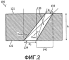
С целью иллюстрирования принципов устройства 100 выбора света и конфигурации световых каналов один из световых каналов 130 показан более подробно на фиг.2. Пропускающие свет участки в этом пояснительном примере имеют форму круга. Первый пропускающий свет участок 133 имеет размер, обусловленный его диаметром d1. Второй пропускающий свет участок 134 имеет второй размер, обусловленный его диаметром d2. Первый и второй пропускающие свет участки 133 и 134 выполнены с боковым смещением 140 так, что угол, обозначенный α, сформирован относительно нормали к первой и второй поверхностям 121, 122. Благодаря компоновке светового канала 130 только свет с углом падения между минимальным углом θmin и максимальным углом θmax может проходить по световому каналу 130. Этот диапазон углов для света, проходящего через два пропускающих свет участка 133 и 134,![]()
![]()
θmin=arctan![]()
![]()
![]()
![]()
θmax=arctan![]()
![]()
![]()
![]()
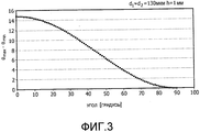
В альтернативном варианте осуществления размеры, а здесь диаметры, первого и второго пропускающих свет участков 133 и 134 равны, так что d1=d2. В неограничивающем примере устройства 100 в этом варианте осуществления селекторный блок 120 снабжен выполненными лазером отверстиями в черной поглощающей пластиковой пластине, т.е. световые каналы выполнены как отверстия, располагающиеся от первой поверхности 121 до второй поверхности 122 пластиковой пластины, чьи отверстия выполнены под разными углами α. Толщина пластины h составляет 1 мм, и первый и второй пропускающие свет участки выполнены с одним и тем же диаметром d1=d2=130 мкм. Угол α отдельных отверстий распределен от 0 до 60 градусов с дискретностью в 5 градусов. Результирующий рассчитанный разрешенный диапазон угла для выбранного света, как функция от угла α, был рассчитан с использованием уравнений 1 и 2 и показан на графике на фиг.3.In an alternative embodiment, the dimensions, and here the diameters, of the first and second
Вторые пропускающие свет участки 134-138 селекторного блока 120 предпочтительно расположены таким образом, который подходит для детекторного блока 110, и более конкретно они расположены, чтобы подобрать подходящий датчик, встроенный в детекторный блок.The second light transmitting portions 134-138 of the selector unit 120 are preferably arranged in a manner that is suitable for the
В одном варианте осуществления устройства вторые пропускающие свет участки расположены близко друг к другу с тем, чтобы выдержать участок датчика 112 как можно малым.In one embodiment of the device, the second light transmitting portions are located close to each other so as to keep the portion of the sensor 112 as small as possible.
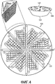
В другом варианте осуществления, как показано на схематичном виде сверху и перспективных видах селекторного блока 120 на фиг.4, множество близко размещенных световых каналов выполнены с множеством углов α в селекторном блоке 420. Световые каналы выполнены так, что детекторный блок 110, который принимает свет, выбранный селекторным блоком 420, будет принимать падающий свет для количества диапазонов углов, соответствующего сформированным световым каналам, на разных положениях детекторного блока 110. В этом варианте осуществления датчик предпочтительно реализован как матрица датчиков, так что каждый отдельный световой канал можно обнаружить на определенном элементе датчика, расположенного на матрице датчиков. Селекторный блок 420 снабжен в общей сложности 97 световыми каналами, каковые световые каналы выполнены как сквозные отверстия, расположенные звездообразно, содержащие подструктуру световых каналов, симметрично расположенных веерно от центра звезды, и чья подструктура повторяется полностью 8 раз. Каждый световой канал в подструктуре (обозначенные 5°, 10°, 15°, 20°, 25°, 30°, 35°, 40°, 45°, 50°, 55° и 60° на фиг.4) располагается под углом радиально и диаметрально по селекторному блоку 420, т.е. от первой поверхности 121 селекторного блока 420 до второй поверхности 122 селекторного блока 420 наклонно под каждым соответствующим углом (5°, 10°, 15°,…, 55°, 60°). Отверстия в поясняющем неограничивающем варианте осуществления имеют диаметр 130 мкм и углы диапазона отверстий между 0 и 60 градусами с дискретизацией в 5 градусов (обозначены на фигуре).In another embodiment, as shown in a schematic top view and perspective views of the selector unit 120 in FIG. 4, a plurality of closely spaced light channels are provided with a plurality of angles α in the
Каждый белый кружок на чертеже обозначает первый пропускающий свет участок на первой (верхней) поверхности 121 селекторного блока 120. Далее каждый пунктирный кружок на чертеже обозначает соответствующий второй пропускающий свет участок на второй (нижней) поверхности 122 селекторного блока 120, в котором каждый набор первого и второго пропускающих свет участков формирует световой канал через селекторный блок. Толщина селекторного блока равна h=1 мм.Each white circle in the drawing indicates a first light transmitting portion on a first (upper)
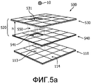
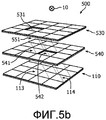
В другом варианте осуществления устройства 500, как показано на фиг.5а) и b), селекторный блок 520 выполнен с использованием двух мозаичных оптических модуляторов 530 и 540, которые расположены параллельно и разделены промежутком h. Термин «мозаичный» относится к наличию анода и катода, входящих в состав пиксельных участков с тем, чтобы обеспечить оптический модулятор адресуемыми пикселями. (Каждый пиксель будет содержать индивидуальный анод и катод, и оптический материал, который может также включать в себя, например фильтр или поляризатор, которые охватываются этим отдельным пиксельным участком). Каждый пиксель может быть отдельно адресованным и, таким образом, связанным с напряжением. Это хорошо известно специалисту в данной области техники и далее здесь описано не будет. В этом поясняющем примере оптические модуляторы 530 и 540 являются, каждый, выполненными для обеспечения структурированной матрицы из 4×4 пикселей. Размер и количество пикселей в каждой матрице пикселей являются произвольными и зависят от требований текущего применения. Каждый пиксель может переключаться из прозрачного состояния в непрозрачное состояние. Под прозрачным состоянием подразумевается состояние, по меньшей мере, с некоторым пропусканием света, т.е. пропускание света не должно быть 100%, но достаточным для того, чтобы отличаться от непрозрачного состояния, в котором по существу нет пропускания света (например, из-за поглощения или отражения). Устройство 500 далее приспособлено для того, чтобы иметь детекторное устройство 110, содержащее массив датчиков в форме 4×4 матрицы элементов датчиков света. Датчики выполнены, например, с фотоприемниками. Как и в случае с пикселями, размер датчиков и количество датчиков в матрице 110 датчиков произвольно и зависит от требований текущего применения.In another embodiment of the
Далее функционализация селекторного устройства 520 объясняется со ссылкой на фиг.5а) и далее ниже на фиг.5b). Свет от источника 10 света достигает первого оптического модулятора 530, в котором все пиксели установлены в непрозрачное состояние, кроме одного пикселя 531, который установлен в прозрачное состояние. Таким образом, прозрачный пиксель 531 соответствует первому пропускающему свет участку. Во втором оптическом модуляторе 540 все пиксели установлены в непрозрачное состояние, кроме пикселя 541, который установлен в прозрачное состояние и далее соответствует второму пропускающему свет участку. Первый и второй пропускающие свет участки (соответствующие пикселю 531 и пикселю 541) формируют световой канал 550. Свет с углами падения, которые разрешены, проходит через селекторное устройство 520 через открытый световой канал 550 и достигает массива датчиков детекторного устройства 110 в элементе 113 датчика.Further, the functionalization of the
На фиг.5b) предыдущий прозрачный пиксель 541 был переключен в непрозрачное состояние, и другой пиксель 542 переключен в прозрачное состояние. Это приводит к образованию измененного светового канала 551 для света, чтобы он проходил через селекторный блок 520. Угол действующего открытого светового канала изменяется, так что свет с другим диапазоном углов падения может проходить через селекторный блок 520 и достигать детекторного блока 110. В то же самое время положение детекторного блока 110, которого достиг свет, изменяется в этом случае для пикселя 114 датчика. Таким образом, активированием различных комбинаций пикселей для двух оптических модуляторов 530 и 540 диапазон разрешенных углов света, проходящего через селекторный блок 120, изменяется, и может быть получен доступ к разным датчикам в детекторном блоке 110.5b), the previous
В одном варианте осуществления устройства, содержащего мозаичные оптические модуляторы, пиксельные матрицы использованы не только, чтобы регулировать угол α световых каналов путем изменения положения отдельных пикселей, т.е. регулировкой бокового смещения 140, установки пары пикселей в прозрачное состояние, но чтобы дополнительно изменять размер (и если нужно форму) пропускающих свет участков. В предыдущем примере единичные пиксели были выполнены как пара пикселей (например, 531 и 542), чтобы создавать световой канал (551). Позвольте нам обсудить случай, когда матрицы оптических модуляторов 530 и 540 выполнены размером 100×100. Тогда может быть установлена комбинация пикселей, чтобы быть прозрачной и сформировать первый излучающий свет участок на первом оптическом модуляторе 530, и соответственно комбинация пикселей на втором оптическом модуляторе 540, чтобы сформировать второй излучающий свет участок. Пиксели могут быть выбраны, чтобы сформировать, в качестве примера, пропускающие свет участки в форме круга, которыми можно управлять переключением подходящих пикселей. Следовательно, регулируемые диаметры (и следовательно размер) пропускающих свет участков достижимы.In one embodiment of a device comprising mosaic optical modulators, pixel arrays are used not only to adjust the angle α of the light channels by changing the position of individual pixels, i.e. adjusting the
В одном варианте осуществления устройства 520, содержащего оптические модуляторы, оптические модуляторы 530 и 540 выполнены с использованием жидкокристаллических (LC) ячеек. Жидкокристаллические ячейки обычно расположены между скрещенными поляризаторами, чтобы было возможно перекрыть свет и, таким образом, было возможно переключить прозрачное состояние в непрозрачное состояние. Прозрачное состояние тогда имеет максимальное пропускание 50% из-за поглощения света в поляризаторах. Различные LC конфигурации применяются в настоящем изобретении, такие как скрученный нематик, гибридно выровненный нематик, вертикально выровненный нематик, ферроэлектрические LC и т.д.In one embodiment of an
В альтернативном варианте осуществления, по меньшей мере, один оптический модулятор в устройстве содержит мозаичный электрофоретический модулятор, в котором заряженные поглощающие частицы могут быть перемещены в пиксельный участок посредством приложения электрического поля. Если частицы находятся в пиксельном участке, свет перекрывается, а если они перемещаются за пределы пиксельного участка, то свет проходит через пиксели. Этот способ из предыдущей области техники описан в E. Kishi и др. «Development of In-Plane EPD» SID Дайджест 2000, стр. 24-27, документ 5.1 и далее здесь обсуждаться не будет.In an alternative embodiment, the at least one optical modulator in the device comprises a mosaic electrophoretic modulator in which charged absorbing particles can be moved to the pixel region by applying an electric field. If the particles are in the pixel section, the light overlaps, and if they move outside the pixel section, then the light passes through the pixels. This prior art technique is described in E. Kishi et al. “Development of In-Plane EPD” SID Digest 2000, pp. 24-27, document 5.1 and hereinafter will not be discussed.
В дополнительном альтернативном варианте осуществления электросмачивание может быть использовано, чтобы выполнить мозаичный оптический модулятор. Мозаичный оптический модулятор содержит поглощающую жидкость в сочетании с прозрачной жидкостью (где одна из жидкостей полярная, а другая неполярная, причем две жидкости не смешиваются). Изменением электрического поля на поверхности пикселей полярная жидкость может быть втянута в пиксель, а потом неполярная жидкость выталкивается из ячейки. Этот эффект называется электросмачиванием. Короче: поглощающая жидкость может быть втянута в пиксель или вытолкнута из пикселя опять приложением напряжения по всей ячейке, в результате переключая пиксель из прозрачного состояния в непрозрачное состояние. См. в качестве ссылки: Nature 425, 383-385 (25 сентября 2003 г.) «Видеоскоростная электронная бумага на основании электросмачивания» Robert A. Hayes, B.J. Feenstra.In a further alternative embodiment, electrowetting may be used to perform a mosaic optical modulator. The mosaic optical modulator contains an absorbing liquid in combination with a transparent liquid (where one of the liquids is polar and the other non-polar, and the two liquids do not mix). By changing the electric field on the surface of the pixels, the polar liquid can be drawn into the pixel, and then the non-polar liquid is pushed out of the cell. This effect is called electro-wetting. In short: the absorbing liquid can be drawn into the pixel or pushed out of the pixel again by applying voltage throughout the cell, as a result of switching the pixel from a transparent state to an opaque state. See by reference: Nature 425, 383-385 (September 25, 2003) “Electrowetting Video-Speed Electronic Paper” by Robert A. Hayes, B.J. Feenstra.
В альтернативном варианте осуществления световое детекторное устройство содержит дополнительные компенсирующие слои, чтобы достичь высокого контраста и компенсировать рассеяние света при больших углах падения падающего света.In an alternative embodiment, the light detector device comprises additional compensating layers to achieve high contrast and compensate for light scattering at large incidence angles of incident light.
В альтернативном варианте осуществления, в котором селекторный блок выполнен с оптическими модуляторами, содержащими жидкокристаллические модуляторы, и пропускающие свет участки состоят из набора пикселей в верхнем модуляторе 530 и набора пикселей в нижнем модуляторе 540, эти пропускающие свет участки находятся в комбинации, допускающей переключение из прозрачного состояния в непрозрачное. Как пример приведен случай использования двух уложенных друг на друга жидкокристаллических ячеек. Как упоминалось выше, жидкокристаллические ячейки обычно располагаются между скрещенными поляризаторами (поляризатором и анализатором). ЖК-ячейки тогда в основном установлены так, что в прозрачном состоянии линейно поляризованный свет (благодаря поляризатору) направляется через ЖК-ячейки и сдвигается по фазе на 90 градусов. Следовательно, свет со сдвигом фазы может выходить из устройства через анализатор. В непрозрачном состоянии ЖК-ячейки не вносят этот сдвиг фазы, и линейно поляризованный свет, входящий через поляризатор, блокируется анализатором. Однако в этом варианте осуществления нет возможности иметь только два поляризатора, один на вершине верхнего модулятора 530 и один на нижней стороне нижнего модулятора 540, чтобы переключать прозрачное состояние в непрозрачное состояние для двух наборов пикселей двух комбинированных модуляторов. В прозрачном состоянии две расположенных друг над другом жидкокристаллических ячейки затем вместе вносят сдвиг фазы на 90 градусов линейно поляризованного света, который вводят модуляторы 530, 540 через поляризатор верхнего модулятора 530. Следовательно, свет может выходить из селекторного блока 520 через анализатор. Поляризатор и анализатор не показаны на чертежах, но хорошо известны в области техники.In an alternative embodiment, in which the selector unit is configured with optical modulators comprising liquid crystal modulators and light transmitting portions consisting of a set of pixels in an
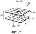
В соответствии с вариантом осуществления изобретения, как показано на фиг.7, световой детектор 700 с выбором угла света содержит единственный мозаичный оптический модулятор 730, который в этом неограничивающем примере представляет собой мозаичную жидкокристаллическую ячейку между перекрещенными поляризаторами. Принцип селекторного блока 720, выбирающего угол света, здесь тот же самый, что и для вариантов осуществления, как описано выше, с той разницей, что здесь вторая поверхность 122 выполнена непосредственно на детекторном блоке 710. К тому же детекторный блок 710 содержит массив световых датчиков, т.е. снабжен адресуемыми элементами светового датчика (или пикселями световых элементов).According to an embodiment of the invention, as shown in FIG. 7, a light detector with a
Когда свет от источника 10 света достигает оптического модулятора 730, он может только проходить через пропускающие свет участки, переключенные в прозрачное состояние. На фиг.7 все пиксели установлены в непрозрачное состояние, кроме одного пикселя 731, который установлен в прозрачное состояние. Таким образом, прозрачный пиксель 731 соответствует первому пропускающему свет участку. Теперь рассмотрим элемент 714 светового датчика. Элемент 714 светового датчика активен и выбирает, т.е. действует как второй пропускающий свет участок, который вместе с первым пропускающим свет участком формирует световой канал 751 от мозаичного оптического модулятора 730 до мозаичного детекторного блока 710 для света с углами падения, находящимися между максимальным углом и минимальным углом. Более того, элемент 714 светового датчика обнаруживает свет, который достигает конкретного местоположения элемента 714 светового датчика. В зависимости от того, какой пиксель или набор пикселей мозаичного оптического модулятора 730 переключен в прозрачное состояние, свет разных диапазонов угла света достигает элемента 714 светового датчика. Так как детекторный блок 710 выполнен с некоторым количеством элементов светового датчика (4×4 на фиг.7), то для каждого элемента светового датчика свет определенных диапазонов угла света достигает элемента светового датчика в зависимости от того, какой пиксель или набор пикселей переключен в прозрачное состояние на оптическом модуляторе 730.When the light from the
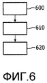
Способ изготовления светового детектора с выбором угла света в соответствии с настоящим изобретением содержит количество этапов, которые необязательно должны быть выполнены в определенном порядке. Далее способ будет описан в неограничивающем примере со ссылкой на фиг.6. На этапе 600 представлен детекторный блок 110. Как описано выше, детекторный блок 110 может быть единичным элементом светового датчика или матрицей элементов светового датчика. Селекторный блок 120 представлен на этапе 610. Разные варианты осуществления селекторного блока описывались выше. Для каждого варианта осуществления этап выполнения селекторного блока 120 напрямую зависит от определенного варианта осуществления. Например, при выполнении селекторного блока в куске материала, такого как поглощающий пластик, световые каналы селекторного блока выполнены сверлением или прожиганием лазером отверстий с разными углами (необязательно с первым и вторым размером) в материале, тогда как при выполнении селекторного блока с двумя сложенными вместе оптическими модуляторами световые каналы реализуются выполнением модуляторов с пикселями, которые могут переключаться из прозрачного состояния в непрозрачное состояние. Функциональность селекторного блока 120 при выполнении его с двумя сложенными вместе оптическими модуляторами описана выше. Оптические модуляторы являются, например жидкокристаллическими модуляторами, или модуляторами, применяющими электросмачивание, которые хорошо знакомы из предыдущего уровня техники, и их изготовление и адресация далее здесь не обсуждаются. Селекторный блок 120 и детекторный блок 110 затем объединяются на этапе 620 так, что детекторный блок может принимать свет, выбранный селекторным блоком 120. Выше были описаны варианты осуществления светового детекторного устройства с выбором угла света в соответствии с настоящим изобретением, как указано в прилагаемой формуле изобретения. Их следует рассматривать просто как неограничивающие примеры. Как понятно специалисту, многие усовершенствования и альтернативные варианты осуществления возможны в объеме изобретения.A method of manufacturing a light detector with a choice of the angle of light in accordance with the present invention contains a number of steps that need not be performed in a specific order. Next, the method will be described in a non-limiting example with reference to Fig.6. At 600, a
Нужно заметить, что для целей этой заявки и, в частности, относительно прилагаемой формулы слово «содержащий» не исключает другие элементы или этапы, что единственное число не исключает множества, что само по себе будет ясно специалисту в данной области техники.It should be noted that for the purposes of this application and, in particular, regarding the attached formula, the word “comprising” does not exclude other elements or steps, that the singular does not exclude a plurality, which in itself will be clear to a person skilled in the art.
Claims (13)
селекторный блок и
детекторный блок, расположенный, чтобы принимать свет, выбранный упомянутым селекторным блоком, причем
упомянутый селекторный блок содержит непрозрачное тело, имеющее первую поверхность и вторую поверхность, причем упомянутые первая и вторая поверхности, по существу, параллельны одна другой, и вертикально разделены промежутком, упомянутое устройство содержит, по меньшей мере, один световой канал, идущий от первого пропускающего свет участка, имеющего первый размер, расположенный на упомянутой первой поверхности, до второго пропускающего свет участка со вторым размером, расположенным на упомянутой второй поверхности, упомянутый первый пропускающий свет участок и упомянутый второй пропускающий свет участок выполнены с боковым смещением, причем упомянутый световой канал позволяет свету с углами падения между максимальным углом и минимальным углом проходить через упомянутый селекторный блок, причем упомянутые углы падения задаются посредством упомянутого первого и второго размера, упомянутого бокового смещения и упомянутого промежутка.1. Light detector device with a choice of the angle of light, containing:
selector block and
a detector unit arranged to receive light selected by said selector unit, wherein
said selector block comprises an opaque body having a first surface and a second surface, said first and second surfaces being substantially parallel to one another and vertically spaced apart, said device comprising at least one light channel coming from a first light transmitting a portion having a first size located on said first surface to a second light-transmitting portion with a second dimension located on said second surface, said first the light-transmitting portion and said second light-transmitting portion are laterally displaced, said light channel allowing light with incidence angles between a maximum angle and a minimum angle to pass through said selector unit, said incidence angles being defined by said first and second sizes, said lateral displacement and the said gap.
обеспечения детекторного блока;
обеспечения селекторного блока в непрозрачном материале, упомянутый селекторный блок имеет первую и вторую поверхности, расположенные параллельно и имеющие промежуток между друг другом;
расположения в упомянутом селекторном блоке, по меньшей мере, одного светового канала, идущего от первого пропускающего свет участка, имеющего первый размер, расположенный на упомянутой первой поверхности, до второго пропускающего свет участка со вторым размером, расположенным на упомянутой второй поверхности,
причем упомянутый первый пропускающий свет участок и второй пропускающий свет участок выполнены с боковым смещением; и
объединения упомянутого детекторного блока с упомянутым селекторным блоком, чтобы принимать свет, выбранный упомянутым селекторным блоком;
причем упомянутый селекторный блок содержит мозаичный оптический модулятор,
упомянутый детекторный блок является мозаичным и составляет часть упомянутого селекторного блока, так что упомянутая вторая поверхность выполнена на упомянутом мозаичном детекторном блоке,
причем упомянутые первый и второй пропускающие свет участки выполнены с первым и вторым набором пикселей, расположенных на упомянутом мозаичном оптическом модуляторе и на упомянутом детекторном блоке соответственно,
причем упомянутый оптический модулятор выполнен с возможностью переключения пикселей между прозрачным состоянием и непрозрачным состоянием.12. A method of manufacturing a light detector with a choice of the angle of incidence, comprising the steps of:
providing a detector unit;
providing a selector unit in an opaque material, said selector unit has first and second surfaces arranged in parallel and having a gap between each other;
the location in said selector unit of at least one light channel extending from a first light transmitting portion having a first size located on said first surface to a second light transmitting portion with a second size located on said second surface,
wherein said first light transmitting portion and a second light transmitting portion are laterally biased; and
combining said detector unit with said selector unit to receive light selected by said selector unit;
wherein said selector unit comprises a mosaic optical modulator,
said detector block is mosaic and constitutes part of said selector block, so that said second surface is formed on said mosaic detector block,
wherein said first and second light transmitting portions are made with a first and second set of pixels located on said mosaic optical modulator and on said detection unit, respectively,
wherein said optical modulator is configured to switch pixels between a transparent state and an opaque state.
Applications Claiming Priority (3)
| Application Number | Priority Date | Filing Date | Title |
|---|---|---|---|
| EP07119349 | 2007-10-26 | ||
| EP07119349.4 | 2007-10-26 | ||
| PCT/IB2008/054333 WO2009053905A2 (en) | 2007-10-26 | 2008-10-21 | A light angle selecting light detector device |
Publications (2)
| Publication Number | Publication Date |
|---|---|
| RU2010121178A RU2010121178A (en) | 2011-12-10 |
| RU2492496C2 true RU2492496C2 (en) | 2013-09-10 |
Family
ID=40473628
Family Applications (1)
| Application Number | Title | Priority Date | Filing Date |
|---|---|---|---|
| RU2010121178/28A RU2492496C2 (en) | 2007-10-26 | 2008-10-21 | Light angle selecting light detector device |
Country Status (8)
| Country | Link |
|---|---|
| US (1) | US8619249B2 (en) |
| EP (1) | EP2205988A2 (en) |
| JP (1) | JP5694772B2 (en) |
| KR (1) | KR101633612B1 (en) |
| CN (1) | CN101836124B (en) |
| RU (1) | RU2492496C2 (en) |
| TW (1) | TW200925563A (en) |
| WO (1) | WO2009053905A2 (en) |
Families Citing this family (18)
| Publication number | Priority date | Publication date | Assignee | Title |
|---|---|---|---|---|
| EP2488841A2 (en) * | 2009-10-16 | 2012-08-22 | Koninklijke Philips Electronics N.V. | A spectral detection device for detecting spectral components of received light |
| JP5725528B2 (en) * | 2010-03-02 | 2015-05-27 | 岩崎電気株式会社 | Beam parallelism measuring device |
| JP2012058140A (en) * | 2010-09-10 | 2012-03-22 | Denso Corp | Optical sensor |
| JP5644395B2 (en) * | 2010-11-10 | 2014-12-24 | 株式会社デンソー | Optical sensor device |
| US8901480B2 (en) * | 2010-09-10 | 2014-12-02 | Denso Corporation | Optical sensor having a blocking film disposed over light receiving elements on a semiconductor substrate via a light transparent film for detecting an incident angle of light |
| JP5724384B2 (en) * | 2011-01-06 | 2015-05-27 | 株式会社デンソー | Optical sensor |
| WO2012145054A1 (en) * | 2011-04-20 | 2012-10-26 | Raytheon Company | Attenuator screen for controlled transmission of electromagnetic energy to an optical sensor for stray light reduction |
| DK2802652T3 (en) | 2012-01-12 | 2019-07-15 | Endo Global Ventures | CLOSTRIDIUM HISTOLYTICS ENZYME |
| TWI563848B (en) * | 2014-06-04 | 2016-12-21 | Sensortek Tech Corp | Light sensing device and method of handling light sensing element thereof |
| JP2016080556A (en) * | 2014-10-20 | 2016-05-16 | 岡谷電機産業株式会社 | Infrared sensor |
| JP2016161458A (en) * | 2015-03-03 | 2016-09-05 | 株式会社デンソー | Optical sensor |
| EP3494372A4 (en) * | 2016-08-04 | 2020-03-25 | Ophir Optronics Solutions Ltd. | A photometric test system for light emitting devices |
| GB201614330D0 (en) | 2016-08-22 | 2016-10-05 | Univ Of Sussex The | Attitude determination system |
| AU2018244426B2 (en) | 2017-03-28 | 2024-09-19 | Endo Ventures Limited | Improved method of producing collagenase |
| EP3820737B1 (en) * | 2018-07-10 | 2023-05-10 | Gentex Corporation | Window control system for limiting light intensity variation |
| US11740723B2 (en) * | 2019-05-02 | 2023-08-29 | Apple Inc. | Electronic devices having light sensors overlapped by displays |
| WO2022074530A1 (en) * | 2020-10-06 | 2022-04-14 | Maytronics Ltd. | Selective optical collection devices and systems using same |
| CN215069988U (en) * | 2021-02-01 | 2021-12-07 | 北京与光科技有限公司 | Spectroscopic chip and spectroscopic analysis device |
Citations (2)
| Publication number | Priority date | Publication date | Assignee | Title |
|---|---|---|---|---|
| GB1454272A (en) * | 1973-07-10 | 1976-11-03 | Secr Defence | Apparatus for monitoring airport runway lights |
| US5148180A (en) * | 1991-07-15 | 1992-09-15 | The United States Of America As Represented By The Secretary Of The Navy | Method and apparatus for passive direction finding with sideband determination |
Family Cites Families (33)
| Publication number | Priority date | Publication date | Assignee | Title |
|---|---|---|---|---|
| US3435246A (en) * | 1966-02-09 | 1969-03-25 | Webb James E | Light radiation direction indicator with a baffle of two parallel grids |
| FR2172828B1 (en) * | 1972-02-23 | 1974-12-13 | Dassault Electronique | |
| CH596621A5 (en) * | 1976-06-30 | 1978-03-15 | Cerberus Ag | |
| JPS55124007A (en) | 1979-03-16 | 1980-09-24 | Nec Corp | Light angle detector |
| US4498767A (en) * | 1982-09-07 | 1985-02-12 | Teletype Corporation | Apparatus for measuring light |
| US4593187A (en) | 1982-10-29 | 1986-06-03 | The Perkin-Elmer Corporation | Non-imaging illumination incidence angle detection system |
| JPS59133477A (en) * | 1983-01-20 | 1984-07-31 | Seiko Instr & Electronics Ltd | Optical angle detector |
| JPS61142428A (en) | 1984-12-17 | 1986-06-30 | Toshiba Corp | Light collimator |
| JPS6216414U (en) * | 1985-07-16 | 1987-01-31 | ||
| JPH0714806Y2 (en) * | 1987-06-16 | 1995-04-10 | システム工業株式会社 | Solar tracking sensor |
| GB2213927A (en) | 1987-12-18 | 1989-08-23 | Philips Electronic Associated | Pyroelectric infrared sensors |
| JPH0327327U (en) * | 1989-07-27 | 1991-03-19 | ||
| DE3940146A1 (en) | 1989-12-05 | 1991-06-06 | Ketterer Klaus | Changing light attenuation passing through glass pane - using LCD cells affected by light impingement angle caused by switchable voltage fields |
| US5012080A (en) * | 1990-04-19 | 1991-04-30 | Griscom Daniel T | Directional particle filter |
| US5170221A (en) * | 1990-06-15 | 1992-12-08 | Okuma Corp. | Parallel light ray measuring apparatus |
| JPH0568611A (en) * | 1991-09-11 | 1993-03-23 | Matsushita Electric Ind Co Ltd | Kitchen equipment |
| JP3057535B2 (en) * | 1992-03-31 | 2000-06-26 | ナイルス部品株式会社 | Optical detector |
| GB2266366B (en) * | 1992-04-16 | 1996-04-24 | Rank Taylor Hobson Ltd | Angle detection |
| JPH0669536A (en) | 1992-08-21 | 1994-03-11 | Nippondenso Co Ltd | Manufacture of light-position detection device |
| JPH08264826A (en) | 1995-03-24 | 1996-10-11 | Hamamatsu Photonics Kk | Photodetector and light incident angle detector |
| DE19544268A1 (en) | 1995-11-28 | 1997-06-05 | Bayer Ag | Process for the preparation of beta-hydroxyalkylpicolinium salts |
| JP2778577B2 (en) | 1996-04-18 | 1998-07-23 | 日本電気株式会社 | Light beam angle detector |
| US5757478A (en) * | 1996-06-03 | 1998-05-26 | Ma; Chris Chen-Hsing | Remote position sensing apparatus and method |
| EP1026558A3 (en) * | 1999-02-05 | 2001-02-07 | Richard Keatch | Sundial |
| JP2000292256A (en) * | 1999-04-05 | 2000-10-20 | Sony Corp | Luminance measuring method and wide-range / wide-angle luminance measuring device |
| US6995800B2 (en) * | 2000-01-27 | 2006-02-07 | Canon Kabushiki Kaisha | Image pickup apparatus utilizing a plurality of converging lenses |
| JP3954373B2 (en) * | 2001-12-05 | 2007-08-08 | 浜松ホトニクス株式会社 | Imaging device |
| JP4091414B2 (en) | 2002-12-18 | 2008-05-28 | 三菱電機株式会社 | Planar light source device, display device, and liquid crystal display device |
| JP3709873B2 (en) * | 2003-02-19 | 2005-10-26 | ソニー株式会社 | Solid-state imaging device and imaging camera |
| WO2004081956A2 (en) | 2003-03-12 | 2004-09-23 | O-Pen Aps | A multitasking radiation sensor |
| WO2007000699A1 (en) * | 2005-06-29 | 2007-01-04 | Koninklijke Philips Electronics N.V. | Control system for controlling the light output of a led luminaire |
| JP2007207789A (en) * | 2006-01-31 | 2007-08-16 | Nara Institute Of Science & Technology | Solid-state imaging device and imaging device using the device |
| US7924415B2 (en) * | 2009-02-19 | 2011-04-12 | The United States Of America As Represented By The Administrator Of The National Aeronautics And Space Administration | Apparatus and method for a light direction sensor |
-
2008
- 2008-10-21 CN CN200880113133.2A patent/CN101836124B/en not_active Expired - Fee Related
- 2008-10-21 EP EP08807984A patent/EP2205988A2/en not_active Ceased
- 2008-10-21 US US12/738,672 patent/US8619249B2/en not_active Expired - Fee Related
- 2008-10-21 RU RU2010121178/28A patent/RU2492496C2/en active
- 2008-10-21 KR KR1020107011526A patent/KR101633612B1/en not_active Expired - Fee Related
- 2008-10-21 JP JP2010530607A patent/JP5694772B2/en not_active Expired - Fee Related
- 2008-10-21 WO PCT/IB2008/054333 patent/WO2009053905A2/en not_active Ceased
- 2008-10-23 TW TW097140713A patent/TW200925563A/en unknown
Patent Citations (2)
| Publication number | Priority date | Publication date | Assignee | Title |
|---|---|---|---|---|
| GB1454272A (en) * | 1973-07-10 | 1976-11-03 | Secr Defence | Apparatus for monitoring airport runway lights |
| US5148180A (en) * | 1991-07-15 | 1992-09-15 | The United States Of America As Represented By The Secretary Of The Navy | Method and apparatus for passive direction finding with sideband determination |
Also Published As
| Publication number | Publication date |
|---|---|
| US8619249B2 (en) | 2013-12-31 |
| WO2009053905A2 (en) | 2009-04-30 |
| RU2010121178A (en) | 2011-12-10 |
| KR101633612B1 (en) | 2016-06-27 |
| CN101836124A (en) | 2010-09-15 |
| US20100238430A1 (en) | 2010-09-23 |
| KR20100087183A (en) | 2010-08-03 |
| CN101836124B (en) | 2016-03-02 |
| EP2205988A2 (en) | 2010-07-14 |
| TW200925563A (en) | 2009-06-16 |
| JP2011504225A (en) | 2011-02-03 |
| JP5694772B2 (en) | 2015-04-01 |
| WO2009053905A3 (en) | 2009-06-18 |
Similar Documents
| Publication | Publication Date | Title |
|---|---|---|
| RU2492496C2 (en) | Light angle selecting light detector device | |
| JP5514188B2 (en) | Controllable light angle selector | |
| US9995623B2 (en) | Ambient light assisted spectroscopy | |
| US9256008B2 (en) | Imaging system comprising microlenses and associated device for detecting a sample | |
| US20100128269A1 (en) | Miniaturized surface plasmon resonance imaging system | |
| JP2011164608A (en) | Display device with electrically switchable field of view for embedded light sensor | |
| CN102575959A (en) | A spectral detection device for detecting spectral components of received light | |
| JP5635988B2 (en) | Spectrum detector | |
| CN109073875B (en) | Lighting module for selectable angle lighting | |
| CN109632660A (en) | Fluid detection panel | |
| CN102928419A (en) | Fluorescence sensor | |
| CN102171545B (en) | Spectral detector comprising a cholesteric liquid crystal mixture | |
| CN112630193A (en) | Angle modulation type SPR sensor based on digital micromirror device and SPR detection equipment | |
| GB2328312A (en) | Mirror controlled display device | |
| CA2857914C (en) | Band pass optical touch sensing apparatus and method | |
| CN108917927A (en) | Dispersion means and spectrometer | |
| US12374153B2 (en) | Electronic device | |
| US10281321B2 (en) | Arrangement for spatially resolved and wavelength-resolved detection of light radiation emitted from at least one OLED or LED | |
| TWM634190U (en) | Adjustable detection module for detecting chips and chip carrier having the same | |
| CN214472762U (en) | DMD-based angle modulation SPR sensor and SPR detection equipment | |
| WO2018020779A1 (en) | Optical measuring device | |
| CN117705763A (en) | Light scattering measuring device |
Legal Events
| Date | Code | Title | Description |
|---|---|---|---|
| PD4A | Correction of name of patent owner | ||
| PC41 | Official registration of the transfer of exclusive right |
Effective date: 20170315 |