KR920006283B1 - Digital signal processing method - Google Patents
Digital signal processing method Download PDFInfo
- Publication number
- KR920006283B1 KR920006283B1 KR1019890001694A KR890001694A KR920006283B1 KR 920006283 B1 KR920006283 B1 KR 920006283B1 KR 1019890001694 A KR1019890001694 A KR 1019890001694A KR 890001694 A KR890001694 A KR 890001694A KR 920006283 B1 KR920006283 B1 KR 920006283B1
- Authority
- KR
- South Korea
- Prior art keywords
- data
- output
- selector
- register
- address
- Prior art date
Links
Images


Classifications
-
- G—PHYSICS
- G06—COMPUTING; CALCULATING OR COUNTING
- G06F—ELECTRIC DIGITAL DATA PROCESSING
- G06F9/00—Arrangements for program control, e.g. control units
- G06F9/06—Arrangements for program control, e.g. control units using stored programs, i.e. using an internal store of processing equipment to receive or retain programs
- G06F9/46—Multiprogramming arrangements
- G06F9/50—Allocation of resources, e.g. of the central processing unit [CPU]
- G06F9/5005—Allocation of resources, e.g. of the central processing unit [CPU] to service a request
- G06F9/5027—Allocation of resources, e.g. of the central processing unit [CPU] to service a request the resource being a machine, e.g. CPUs, Servers, Terminals
- G06F9/505—Allocation of resources, e.g. of the central processing unit [CPU] to service a request the resource being a machine, e.g. CPUs, Servers, Terminals considering the load
-
- G—PHYSICS
- G06—COMPUTING; CALCULATING OR COUNTING
- G06F—ELECTRIC DIGITAL DATA PROCESSING
- G06F9/00—Arrangements for program control, e.g. control units
- G06F9/06—Arrangements for program control, e.g. control units using stored programs, i.e. using an internal store of processing equipment to receive or retain programs
- G06F9/46—Multiprogramming arrangements
- G06F9/50—Allocation of resources, e.g. of the central processing unit [CPU]
- G06F9/5061—Partitioning or combining of resources
- G06F9/5066—Algorithms for mapping a plurality of inter-dependent sub-tasks onto a plurality of physical CPUs
-
- G—PHYSICS
- G06—COMPUTING; CALCULATING OR COUNTING
- G06T—IMAGE DATA PROCESSING OR GENERATION, IN GENERAL
- G06T7/00—Image analysis
- G06T7/20—Analysis of motion
- G06T7/223—Analysis of motion using block-matching
-
- H—ELECTRICITY
- H04—ELECTRIC COMMUNICATION TECHNIQUE
- H04N—PICTORIAL COMMUNICATION, e.g. TELEVISION
- H04N19/00—Methods or arrangements for coding, decoding, compressing or decompressing digital video signals
- H04N19/42—Methods or arrangements for coding, decoding, compressing or decompressing digital video signals characterised by implementation details or hardware specially adapted for video compression or decompression, e.g. dedicated software implementation
- H04N19/43—Hardware specially adapted for motion estimation or compensation
- H04N19/433—Hardware specially adapted for motion estimation or compensation characterised by techniques for memory access
-
- H—ELECTRICITY
- H04—ELECTRIC COMMUNICATION TECHNIQUE
- H04N—PICTORIAL COMMUNICATION, e.g. TELEVISION
- H04N19/00—Methods or arrangements for coding, decoding, compressing or decompressing digital video signals
- H04N19/50—Methods or arrangements for coding, decoding, compressing or decompressing digital video signals using predictive coding
- H04N19/503—Methods or arrangements for coding, decoding, compressing or decompressing digital video signals using predictive coding involving temporal prediction
- H04N19/51—Motion estimation or motion compensation
-
- H—ELECTRICITY
- H04—ELECTRIC COMMUNICATION TECHNIQUE
- H04N—PICTORIAL COMMUNICATION, e.g. TELEVISION
- H04N19/00—Methods or arrangements for coding, decoding, compressing or decompressing digital video signals
- H04N19/60—Methods or arrangements for coding, decoding, compressing or decompressing digital video signals using transform coding
- H04N19/61—Methods or arrangements for coding, decoding, compressing or decompressing digital video signals using transform coding in combination with predictive coding
-
- G—PHYSICS
- G06—COMPUTING; CALCULATING OR COUNTING
- G06T—IMAGE DATA PROCESSING OR GENERATION, IN GENERAL
- G06T2207/00—Indexing scheme for image analysis or image enhancement
- G06T2207/10—Image acquisition modality
- G06T2207/10016—Video; Image sequence
-
- H—ELECTRICITY
- H04—ELECTRIC COMMUNICATION TECHNIQUE
- H04N—PICTORIAL COMMUNICATION, e.g. TELEVISION
- H04N19/00—Methods or arrangements for coding, decoding, compressing or decompressing digital video signals
- H04N19/30—Methods or arrangements for coding, decoding, compressing or decompressing digital video signals using hierarchical techniques, e.g. scalability
Abstract
내용 없음.No content.
Description
제1도는 본 발명의 1실시예에 의한 디지탈신호 처리방식의 구성을 도시한 블럭도.1 is a block diagram showing the configuration of a digital signal processing method according to an embodiment of the present invention.
제2도는 본 발명의 1실시예에 의한 3입력 1출력의 연산처리의 흐름도.2 is a flowchart of arithmetic processing of three input and one output according to an embodiment of the present invention.
제3도는 종래의 디지탈신호 처리방식의 구성을 도시한 블럭도.3 is a block diagram showing the configuration of a conventional digital signal processing method.
제4도는 제3도의 디지탈신호 처리방식의 연산처리의 흐름도.4 is a flowchart of arithmetic processing of the digital signal processing method of FIG.
*도면의 주요부분에 대한 부호의 설명* Explanation of symbols for main parts of the drawings
20∼23 : 어드레스 생성기 24∼26 : 데이타 메모리20 to 23:
33 : 레지스터 34∼37 : 셀렉터33: register 34 to 37: selector
34, 35 : 제1의 셀렉터군 36, 37 : 제2의 셀렉터군34, 35:
38 : 연산기 40 : 승산기38: calculator 40: multiplier
42 : 출력셀렉터 43 : 가산기42: output selector 43: adder
44 : 어큐뮬레이터44: accumulator
본 발명은 디지탈신호 계열을 대상으로 연산처리를 행하는 디지탈신호 처리방식에 관한 것이다. 제3도는, 예를들면 1986년도 일본 통신학회 통신부문 전국대회 심포지움 예고(No. S10-1)에 개시된 종래의 디지탈신호 처리방식의 블럭도이며, 도면에서(1)은 동시에 2개의 데이타를 리드하고 라이트할 수 있는 듀질포트 내부데이타 메모리(2P-RAM이라 한다). (2)는 리드 또는 라이트 데이타의 어드레스를 산출하는 어드레스 생성부, (3)은 연산에 따른 데이타의 내부 전송에 사용되는 데이타버스, (4) 및 (5)는 2P-RAM(1)내의 데이타를 선택하는 셀렉터, (6)은 셀렉터(4)에서 선택원 피연산 데이타를 유지하는 레지스터, (7)은 셀렉터(5)에서 선택된 연산데이타를 유지하는 레지스터, (8)은 승산기, (9)는 승산기(8)의 출력을 유지하는 레지스터이다. (10)은 레지스터 (6)의 출력과 어큐뮬레이터(ACC0∼ACC3)(14)의 출력을 선택하는 셀렉터, (11)은 레지스터(9)의 출력과 레지스터(7)의 출력을 선택하는 셀렉터, (12)는 셀렉터(10), (11)의 출력을 입력해서 연산을 행하는 산술논리연산기, (13)은 이 산술논리연산기(12)의 출력과 외부용 데이타 레지스터(16)의 데이타를 선택하는 셀렉터이다.The present invention relates to a digital signal processing method that performs arithmetic processing on a digital signal sequence. 3 is a block diagram of a conventional digital signal processing method disclosed in, for example, the 1986 Japanese Telecommunications Society National Conference Symposium Notice (No. S10-1), where (1) reads two data at the same time. Duzile port internal data memory (called 2P-RAM). (2) is an address generator which calculates an address of read or write data, (3) is a data bus used for internal transfer of data by operation, and (4) and (5) are data in 2P-RAM (1). Selector (6) is a register holding selector operand data in selector (4), (7) is a register holding operation data selected in selector (5), (8) is a multiplier, (9) Is a register holding the output of the multiplier 8. (10) is a selector for selecting the output of the register (6) and the outputs of the accumulators (ACC0 to ACC3) 14, (11) is a selector for selecting the output of the register (9) and the output of the register (7), ( 12 is an arithmetic logic operator that inputs the outputs of the
상기 어큐물레이터(14)는 연산기(12)의 출력을 유지하여 누산등에 사용하는 어큐뮬레이터이다. 또, 상기 외부용 데이타 레지스터(16)은 외부데이타 메모리(17)의 데이타를 유지하는 것이다. (15)는 어드레스 생성부(2)에서 생성된 어드레스 데이타를 유지하여 외부 메모리(17)에 전송하는 외부용 어드레스 레지스터이다.The accumulator 14 is an accumulator for holding the output of the calculator 12 and accumulating it. The
다음에 동작에 대해서 설명한다. 본 발명은 내장된 마이크로 프로그램의 페치디코드 및 데이타의 리드, 연산, 연산결과 라이트를 병렬 파이프라인 처리로 실행하는 디지탈신호 처리 프로세서에 의한 처리를 행하는 것이며, 3입력 1출력 연산을 행하는 경우의 동작을 다음에 나타낸다. 단, 연산기, 승산기, 어드레스 생성기, 데이타 메모리, 셀렉터등의 각부는 명령마이크로모드에 따라서 제어된다. 가산, 감산, 최대값, 최소값등을 구하는 2입력 산술연산을 모아서 a![]()
![]()

단, ai, bi, ci는 각각 독립적인 데이타 계열로 하여 2P-RAM(1)에 기억되어 있는 것으로 한다. 예를들면, (1)식의 3입력 연산을 제3도의 디지탈신호 처리방식으로 실행하는 경우의 처리흐름을 제4도에 도시한다.However, it is assumed that ai, bi and ci are stored in the 2P-RAM 1 as independent data series. For example, FIG. 4 shows a processing flow in the case where the three-input operation of expression (1) is executed by the digital signal processing method of FIG.
실제의디지탈신호 처리 프로세서인 DSSP1(Digital Speech Signal Processor 1)에서는 제3도의 데이타어드레스 생성부(2)에서 데이타용 어드레스 값을 2개의 네이타 계열A및B의 각각의 선두 어드레스에 설정하고 단순 인크리멘트의 모드로한 후, 순차적으로 2개의 데이타 계열 A 및 B의 데이타를 2P-RAM(1)에서 셀렉터(4), (5)를 거쳐서 레지스터(6) 및 레지스터(7)로 한다. 셀렉터(10) 빛 (11)에서는 각각 레지스터(6) 및 레지스터(7)측을 선택하여 산술논리연산기 (12)로 산술연산(ai![]()
![]()
다음에 스텝 ST3에서 재차 데이타 어드레스 생성부(2)에서 데이타용 어드레스값을 데이타계열C및 (ai![]()
![]()
한편, 외부메모리(17)에서 (ai![]()
![]()
![]()
![]()
이상의 동작을 파이프라인 처리에 의해 병렬동작이 행하여지기 때문에 N개의 데이타 계열에 대해서 2P-RAM(1)에서 리드하고 나서 처리결과를 외부메모리(17)에 기억할 때까지 산술연산인 경우 (N+3)기계사이클을 요한다.Since the parallel operation is performed by the pipeline process, the above operation is performed by reading from 2P-RAM (1) for N data series and then performing arithmetic until storing the result in the external memory (N + 3). Requires a mechanical cycle.
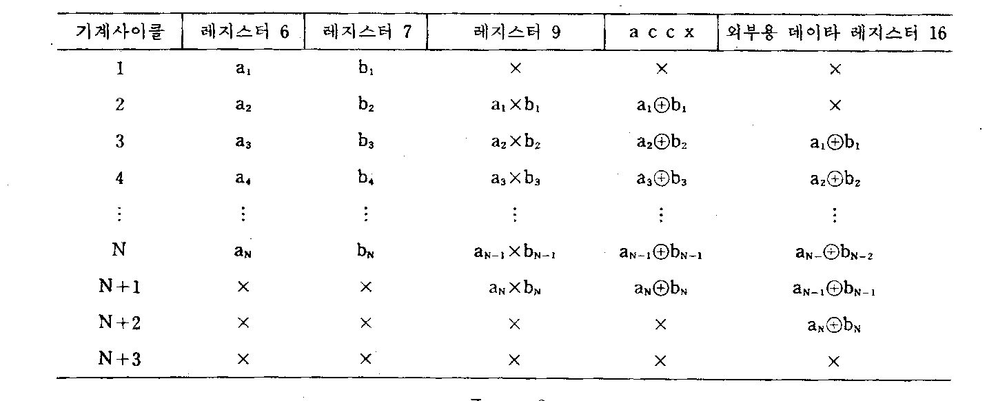
이 상태를 다음의 표1 및 표2에 도시한다.This state is shown in Tables 1 and 2 below.
표1은 (ai![]()
![]()
![]()
![]()
![]()
![]()
[표 1]TABLE 1
[표 2]TABLE 2

다음에 외부메모리(17)에서 빈 리드를 2회 행한 후(타이밍 맞춤), N개의 데이타 계열로 승산을 행하여 2P-RAM(1)로 저장하는데 (N+3) 기계사이클, 그 밖의 어드레스 초기설정에 2명령을 필요로 하기 때문에 합계사이클은 (2N+10)사이클로 원다. (2)식의 연산에 대해서도 (2N+10)사이클을 요한다. 이상과 같이 N개의 데이타 계열에 대하여 3입력 1출력 연산을 DSSP1과 같은 최대 2입력 연산밖에 행할 수 없는 프로세서로 실행하면, 약 2N 기계사이클(N이 충분히 큰 경우)이 필요하다는 것을 알 수 있다.Next, after performing an empty read twice in the external memory 17 (timing alignment), the data is multiplied into N data series and stored in the 2P-RAM (1) (N + 3). The total cycle is wanted as (2N + 10) cycles because 2 instructions are required. (2N + 10) cycles are also required for the calculation in (2). As described above, when a three-input one-output operation is performed on a N data series by a processor that can perform only a maximum of two input operations such as DSSP1, it can be seen that about 2N machine cycles are required (where N is large enough).
또, 상기 3입력 1출력의 연산결과를 누산하는 경우를 다음에 설명한다.The case of accumulating the calculation results of the three inputs and one output will be described next.

(3)식의 경우, (ai![]()
![]()
![]()
![]()
종래의 디지탈신호 처리방식은 이상과 같이 구성되어 있으므로, 3개의 각각 독립된 데이타 계열에 대한 3입력 1출력의 연산을 실행하는 경우, 3입력 1출력의 연산을 2단계로 나누어서 2입력 1출력의 연산을 2회 행하는 것 이외에 어드레스 제어나 메모리로의 전송등의 처리를 위해 연산처리 시간이 길게 된다는 문제점이 있었다.Since the conventional digital signal processing method is configured as described above, when performing the operation of the three input one output for three independent data series, the operation of the two input one output is divided into two stages by the operation of the three input one output. In addition to performing the operation twice, there is a problem that the operation processing time becomes long for processing such as address control and transfer to the memory.
본 발명의 목적은 상기와 같은 문제점을 해결하기 위하여 이루어진 것으로, 3입력 1출력의 연산을 한번에 실행할 수 있음과 동시에 중간결과 저장을 위한 어드레스 제어나 메모리로의 전송등의 처리를 생략할 수가 있어 고속으로 3입력 1출력의 연산을 실행할 수 있는 디지탈신호 처리방식을 얻는 데 있다.The object of the present invention is to solve the above problems, and it is possible to execute three input and one output operation at the same time, and to omit processing such as address control or transfer to memory for storing intermediate results. Therefore, the present invention provides a digital signal processing method capable of performing three input and one output operation.
본 발명에 관한 디지탈신호 처리방식은 3개의 독립된 데이타 계열에 대하여 각각 독립적이고, 동시에 데이타의 리드를 행할 수 있도록 한 제1 내지 제3의 리드데이타용 어드레스 생성기와 서로의 출력을 입력으로써 산술연산과 승산의 조합에 의한 3입력 1출력의 연산을 고속으로 실행하도록 한 연산기와 승산기를 마련한 것이다.The digital signal processing method according to the present invention is arithmetic operation by inputting each of the first to third read data address generators which are independent of each of three independent data series and which can read data at the same time. A multiplier and a multiplier are provided to execute a three-input-one-output operation by a combination of multiplications at high speed.
본 발명에서 제1 내지 제3의 리드데이타를 어드레스 생성기에서 3개의 독립원 데이타계열에 대해서 각각 독립적이고 동시에 데이타를 리드해서 이 리드한 데이타를 연산기에 전송헤서 산술연산을 행함과 동시에, 승산기로 승산을 행하고, 연산기 또는 승산기의 출력을 일시에 메모리에서 물러나게 하지 않고, 다음의 스텝에서 연산기의 출력을 승산기에 부가하고, 승산기의 출력을 연산기에 부가하여 산술연산과 승산의 조합으로 3입력 1출력의 연산을 고속으로 실행할 수 있다.In the present invention, the first to third read data are independently and simultaneously read from each of three independent source data sequences in the address generator, the read data is transferred to an arithmetic operator, and multiplied by a multiplier. In the following step, the output of the operator is added to the multiplier, and the output of the multiplier is added to the calculator, and the combination of arithmetic and multiplication is performed. The operation can be executed at high speed.
이하, 본 발명의 1실시예를 도면에 따라서 설명한다. 제1도에서(20), (21), (22)는 리드데이다용 어드레스생성기, (23)은 라이트 데이타용 어드레스 생성기, (24), (25), (26)은 데이타 메모리로써, 라이트 데이타용 어드레스 생성기(23)에서 생성된 어드레스 데이타가 입력된다. (27), (28), (29)는 데이타 메모리(24), (25), (26)에서의 리드데이타를 전송하는 데이타버스, (30), (31), (32)는 각각 상기 데이타 버스(27), (28), (29)에서 전송되는 데이타를 유지하는 레지스터, (33)은 레지스터(32)의 출력을 유지하는 레지스터이다. (34)는 레지스터(30)과 레지스터(33)의 출력을 선택하는 셀렉터, (35)는 레지스터(31)의 출력과 레지스터(41)의 출력을 선택하는 셀렉터이고, 셀렉터(34)와 (35)로 제1의 셀랙터군을 이루고 있다. (36)은 레지스터(30)의 출력과 레지스터(39)의 출력을 선택하는 셀렉터, (37)은 레지스터(31)의 출력과 레지스터(33)의 출력을 선택하는 셀렉터이고, 셀렉터(36)과 (37)은 제2의 셀렉터군을 이루고 있다. (38)은 쎌렉터(34)와 (35)의 출력을 입력으로 하여 연산을 행하는 연산기, (40)은 셀렉터(36)과 (37)의 출력을 입력으로 하여 승산을 행하는 승산기이다. 또, 레지스터(39)는 상기 연산기(38)의 출력을 유지하는 레지스터이며, 레지스터(41)은 승산기(40)의 출력을 유지하는 레지스터이다. (42)는 2개의 레지스터(39)와 (41)에서의 입력중, 1개를 선택해서 출력하는 셀렉터, (43)은 출력셀렉터(42)의 출력과 어큐뮬레이터(44)의 출력을 가산하는 가산기이며, 그 출력은 상기 어큐뮬레이터(44)에 출력하도록 하고 있다. (45)는 상기 어큐뮬레이터(44), 출력셀렉터(42)의 출력데이타를 전송하는 데이타버스, (46)은 외부와의 데이타 입출력을 행하는 외부인터페이스회로이다. 또한, (101) ∼(103), (111) ∼(113), (121) ∼(123)은 각각 상기 데이타 메모리(24), (25), (26)의 출력을 데이타버스(27), (28), (29)에 출력하는 신호선을 표시한다.EMBODIMENT OF THE INVENTION Hereinafter, one Embodiment of this invention is described according to drawing. In Fig. 1,
다음에 동작에 대해서 설명한다. 제1도에서 N개의 요소를 갖는 데이타계열A={ai | i=1∼N},B={ai | i=1∼N,C={ci |i=1∼N}이 사전에 각각 데이타 메모리(24), 데이타 메모리(25) 및 데이타 메모리(26)에 저장되어 있는 것으로 한다. 상기의 조건에 따라 3입력 1출력의 연산을 행하는 경우의 동작을 다음에 나타낸다. 또, 그 연산처리흐름을 제2도에 도시한다. 먼저, 스타트해서 스텝 ST11에서 첫번째로 입력데이타 3계열 및 출력결과 저장장소의 선두어드레스를 각각 이 어드레스 생성기(20)∼(23)에 의해 초기 설정한다. 그후, 어드레스 생성기는 단순 인크리엔트 동작으로 한다. 데이타 메모리(24)는 어드레스 생성기(20), 데이타 메모리(25)는 어드레스 생성기(21), 데이타 메모리(26)은 어드레스 생성기(22)와 각각 대응하고 있으며, 각 데이타 메모리(24)∼(26)은 어드레스 생성기(20)∼(22)의 어드레스에 따라서 데이타를 리드한다.Next, the operation will be described. In FIG. 1, the data series A = {ai | i = 1 to N}, B = {ai | It is assumed that i = 1 to N and C = {ci | i = 1 to N} are stored in the
단, 3개의 데이타버스(27) ∼(29) (X-BUS, Y-BUS, Z-BUS)에 대하여 각각 데이타 메모리(24) ∼(26)에서 입력가능하기 때문에 각 데이타 메모리(24)∼(26)에서의 특정의 데이타 버스에 대한 출력은 3개중 1개만 유효로 하고, 나머지 2개는 하이 임피던스상태로 되도록 제어한다. 이때, 데이타 버스의 출력은 유효로한 1개의 데이타로 된다. 예를들면, 레지스터(30)에A의 데이타 계열을 입력하는 경우, 신호선(101)로A계열의 데이타를 출력하고, 그 밖의 데이타메모리(25), (26)에서 데이타 버스(27)로의 출력신호선(111) 및 신호선(121)은 하이임피던스 상태로 한다. 그밖의 데이타 버스에 대해서도 마찬가지이다.However, since each of three
이상과 같이 해서 레지스터(30), (31), (32)에 각 데이타계열의 데이타를 세트한다. 또한, 3개의 데이타 버스(27)∼(29)는 각각 3개의 데이타 메모리(24)∼(26)에서 데이타를 선택할 수 있으므로, 레지스터(30)-(32)로의 데이타 세트의 조합은 33정도 가능하다.The data of each data series is set in the
이하, 3입력 연산으로써 다음의 2식을 정의하고, 그 처리 방법을 나타낸다.Hereinafter, the following two expressions are defined as three input operations, and the processing method is shown.

단, (x![]()
![]()
[표 3a]TABLE 3a

[표 3b]TABLE 3b

먼저, 스텝 ST12에서 셀렉터(34)로 레지스터(30)측을, 셀렉터(35)로 레지스터(31)측을 선택한다. 그 2개가 선택된 데이타(ai 및 bi)를 연산기(38)로 연산(ai![]()
![]()
한편, 레지스터(32)의 데이타ci는 레지스터(33)에 의해 1스텝 지연시켜진다. 다음의 스텝에서는 셀렉터(36)으로 레지스터(39)축을, 셀렉터(37)로 레지스터(33)측을 각각 선택하고, 이 2개의 데이타(ai![]()
![]()
![]()
![]()
![]()
![]()
이와 같이, 본 발명에서는 데이타리드, 연산실행, 데이타 라이트를 파이프라인 처리에 의해 연속실행하는 것에 의해 각 부의 동작제어를 병렬로 동작시킬 수가 있다. 따라서, 상기의 3입력 1출력의 연산동작을 N개의 요소를 갖는 데이타계열에 대하여 집행한 경우, 선두 데이타를 리드하고 나서 최종 데이타 처리결과를 메모리에 라이트할 때까지 (N+3)사이클을 요한다.As described above, in the present invention, the operation control of each unit can be operated in parallel by continuously executing data reads, arithmetic executions, and data writes by pipeline processing. Therefore, when the above-described three-input-output operation is executed for a data sequence having N elements, a (N + 3) cycle is required from reading the leading data to writing the final data processing result into the memory. .
다음에 (2)식의 처리흐름의 설명을 다음의 표4에 나타낸다. 또한, 이 표4의 "X"표는 미지수를 나타낸다.Next, the description of the processing flow of Equation (2) is shown in Table 4 below. In addition, the "X" table of this Table 4 shows an unknown number.
[표 4]TABLE 4

3입력 데이타를 레지스터(30)∼(32)로 리드하는 동작은 상기(1)식의 경우와 마찬가지이다. (2)식을 실행하는 경우, 셀렉터(36)으로 레지스터(30)측을, 셀렉터(37)로 레지스터(31)측을 선택하고, 승산기(40)에 의해 (ai×bi)를 실행하여 그 결과를 레지스터(41)에 세트한다.The operation of reading the three input data into the
다음의 스텝에서는 셀렉터(34)로 레지스터(33)측을, 셀렉터(35)로 레지스터(41)측을 선택하고, 연산기(38)에 의해 (ai×bi)![]()
![]()
이와 같이 하는 것에 의해 (2)식의 경우에 대해서도 (1)식의 경우와 마찬가지로 (N+3)의 사이클을 요한다.By doing in this way, the case of Formula (2) also requires the cycle of (N + 3) similarly to the case of Formula (1).
또한, 2입력 1출력의 연산에 대해서 (ai![]()
![]()
이상에서 3입력 1출력의 연산처리 속도는 DSSP1에 비해서((2N+10)/(N+7))배, 즉 N이 큰 경우는 약2배의 처리속도로 된다. 또, 상기 3입력 1출력의 연산의 누산을 구하는 경우, 중간까지의 누산결과 또는 초기값을 어큐뮬레이터(44)에 저장하고 순차적으로 3입력 1출력의 연산결과와 상기 어큐뮬레이터(44)를 가산기(43)에 의해 가산 후, 재차 어큐뮬레이터(44)에 저장하는 처리를 반복하는 것에 의해 행한다. 따라서, 누산을 행하는 것에 의해 처리 사이클수가 늘어나는 일은 없다.The computational processing speed of the three inputs and one output is about ((2N + 10) / (N + 7)) times that of DSSP1, that is, about N when the N is large. When accumulating the calculation of the three input one output, the accumulation result or the initial value up to the middle is stored in the
이상과 같이 본 발명에 의하면, 독립된 3계열의 데이타를 동시에 리드함과 동시에 연산기의 출력을 승산기로 입력 가능하게 하고, 한쪽 승산기의 출력을 연산기로 입력 가능하게 함과 동시에, 셀렉터에 의해 상기연산기와 승산기의 입력 및 출력을 선별 제어하도록 구성하였으므로, 3입력1출력의 연산의 조합순서를 가변으로 하고, 또한 중간의 연산결과를 저장하기 위한 어드레스 제어나 메모리로서 전송처리를 생략하여 고속으로 3입력 1출력의 연산결과를 실행할 수 있는 효과가 있다.As described above, according to the present invention, it is possible to simultaneously read data of three independent sequences and to input the output of the calculator to the multiplier, to enable the output of one multiplier to be input to the calculator, and by means of the selector. Since the input and output of the multiplier are configured to be selectively controlled, the combination order of the operations of the three inputs and one output is variable, and the address control and the transfer processing as the memory for storing the intermediate calculation results are omitted, and the three inputs 1 are fast. This has the effect of executing the operation result of the output.
Claims (1)
Priority Applications (3)
| Application Number | Priority Date | Filing Date | Title |
|---|---|---|---|
| KR1019920008822A KR920006286B1 (en) | 1988-02-19 | 1992-05-25 | Calculation method for movement compensation |
| KR1019920008820A KR920006284B1 (en) | 1988-02-19 | 1992-05-25 | Information encoding apparatus |
| KR1019920008821A KR920006285B1 (en) | 1988-02-19 | 1992-05-25 | Signal processing apparatus of real-time multi-processor type |
Applications Claiming Priority (8)
| Application Number | Priority Date | Filing Date | Title |
|---|---|---|---|
| JP63037921A JPH01211162A (en) | 1988-02-19 | 1988-02-19 | Real time multi-processor-type signal processor |
| JP63-37921 | 1988-02-19 | ||
| JP63063695A JPH01237838A (en) | 1988-03-18 | 1988-03-18 | Digital signal processing system |
| JP63-63695 | 1988-03-18 | ||
| JP63298723A JPH02145077A (en) | 1988-11-26 | 1988-11-26 | Information encoder |
| JP63-298723 | 1988-11-26 | ||
| JP63-298722 | 1988-11-26 | ||
| JP63298722A JPH02145079A (en) | 1988-11-26 | 1988-11-26 | Movement compensated calculation method |
Related Child Applications (3)
| Application Number | Title | Priority Date | Filing Date |
|---|---|---|---|
| KR1019920008821A Division KR920006285B1 (en) | 1988-02-19 | 1992-05-25 | Signal processing apparatus of real-time multi-processor type |
| KR1019920008822A Division KR920006286B1 (en) | 1988-02-19 | 1992-05-25 | Calculation method for movement compensation |
| KR1019920008820A Division KR920006284B1 (en) | 1988-02-19 | 1992-05-25 | Information encoding apparatus |
Publications (2)
| Publication Number | Publication Date |
|---|---|
| KR890013558A KR890013558A (en) | 1989-09-23 |
| KR920006283B1 true KR920006283B1 (en) | 1992-08-03 |
Family
ID=27460495
Family Applications (1)
| Application Number | Title | Priority Date | Filing Date |
|---|---|---|---|
| KR1019890001694A KR920006283B1 (en) | 1988-02-19 | 1989-02-14 | Digital signal processing method |
Country Status (5)
| Country | Link |
|---|---|
| US (1) | US5155852A (en) |
| EP (3) | EP0703533B1 (en) |
| KR (1) | KR920006283B1 (en) |
| CA (1) | CA1317680C (en) |
| DE (3) | DE68929100T2 (en) |
Families Citing this family (38)
| Publication number | Priority date | Publication date | Assignee | Title |
|---|---|---|---|---|
| EP0843254A3 (en) * | 1990-01-18 | 1999-08-18 | National Semiconductor Corporation | Integrated digital signal processor/general purpose CPU with shared internal memory |
| US5475770A (en) * | 1990-09-24 | 1995-12-12 | Cgk Computer Gesellschaft Konstanz Mbh | Parallel recognition of document images with a time-elapsed processing abortion to improve overall throughput |
| JP2906792B2 (en) * | 1991-11-15 | 1999-06-21 | 日本電気株式会社 | Digital processor and control method thereof |
| KR100254956B1 (en) * | 1991-12-23 | 2002-12-18 | 코닌클리케 필립스 일렉트로닉스 엔.브이. | Recursive Video Signal Processor |
| US6965644B2 (en) * | 1992-02-19 | 2005-11-15 | 8×8, Inc. | Programmable architecture and methods for motion estimation |
| US5440721A (en) * | 1992-03-24 | 1995-08-08 | Sony Electronics, Inc. | Method and apparatus for controlling signal timing of cascaded signal processing units |
| JPH05324583A (en) * | 1992-05-26 | 1993-12-07 | Dainippon Screen Mfg Co Ltd | Image data processor |
| US5499375A (en) * | 1993-06-03 | 1996-03-12 | Texas Instruments Incorporated | Feedback register configuration for a synchronous vector processor employing delayed and non-delayed algorithms |
| JP3482660B2 (en) * | 1993-09-08 | 2003-12-22 | ソニー株式会社 | Image data processing apparatus and image data processing method |
| US5590350A (en) * | 1993-11-30 | 1996-12-31 | Texas Instruments Incorporated | Three input arithmetic logic unit with mask generator |
| KR970002394B1 (en) * | 1994-05-09 | 1997-03-05 | 삼성전자 주식회사 | A data transmission circuit for arithematic logic unit between multiadder |
| JPH0954761A (en) * | 1995-08-15 | 1997-02-25 | Sony Corp | Digital signal processor and information processing system |
| JP3729540B2 (en) * | 1995-09-08 | 2005-12-21 | 株式会社ルネサステクノロジ | Image processing device |
| US5987181A (en) * | 1995-10-12 | 1999-11-16 | Sharp Kabushiki Kaisha | Coding and decoding apparatus which transmits and receives tool information for constructing decoding scheme |
| DE19625569A1 (en) * | 1996-06-26 | 1998-01-02 | Philips Patentverwaltung | Signal processor |
| US5920353A (en) * | 1996-12-03 | 1999-07-06 | St Microelectronics, Inc. | Multi-standard decompression and/or compression device |
| DE19703251A1 (en) * | 1997-01-29 | 1998-11-05 | Kuhn Peter Dipl Ing | A flexible VLSI architecture for block matching and luminance correction |
| US5911082A (en) * | 1997-02-25 | 1999-06-08 | Audio Digitalimaging Inc. | Parallel processing building block chip |
| US6047081A (en) * | 1997-10-24 | 2000-04-04 | Imation Corp. | Image processing software system having configurable communication pipelines |
| JP2000020424A (en) * | 1998-06-26 | 2000-01-21 | Class Technology:Kk | System and method for inter-application communication and computer readable record medium recording the same method |
| US6349378B1 (en) * | 1999-03-31 | 2002-02-19 | U.S. Philips Corporation | Data processing using various data processors |
| US6925641B1 (en) | 2000-02-04 | 2005-08-02 | Xronix Communications, Inc. | Real time DSP load management system |
| US6912576B1 (en) | 2000-05-04 | 2005-06-28 | Broadcom Corporation | System and method of processing data flow in multi-channel, multi-service environment by dynamically allocating a socket |
| US7016412B1 (en) | 2000-08-29 | 2006-03-21 | Koninklijke Philips Electronics N.V. | System and method for dynamic adaptive decoding of scalable video to balance CPU load |
| US9800608B2 (en) | 2000-09-25 | 2017-10-24 | Symantec Corporation | Processing data flows with a data flow processor |
| US9525696B2 (en) | 2000-09-25 | 2016-12-20 | Blue Coat Systems, Inc. | Systems and methods for processing data flows |
| US20020165947A1 (en) | 2000-09-25 | 2002-11-07 | Crossbeam Systems, Inc. | Network application apparatus |
| US20070192863A1 (en) | 2005-07-01 | 2007-08-16 | Harsh Kapoor | Systems and methods for processing data flows |
| US8010469B2 (en) | 2000-09-25 | 2011-08-30 | Crossbeam Systems, Inc. | Systems and methods for processing data flows |
| JP3709553B2 (en) * | 2000-12-19 | 2005-10-26 | インターナショナル・ビジネス・マシーンズ・コーポレーション | Arithmetic circuit and arithmetic method |
| EP1229445A1 (en) * | 2001-02-02 | 2002-08-07 | Cluster Labs GmbH | Method and apparatus for operating a computer system |
| JP2004186978A (en) * | 2002-12-03 | 2004-07-02 | Sanyo Electric Co Ltd | Method and device for data write and digital camera |
| US7660469B2 (en) * | 2003-10-30 | 2010-02-09 | Nec Electronics Corporation | Image decoding apparatus and image decoding method |
| DE102005020808B3 (en) * | 2005-05-04 | 2006-07-20 | Micronas Gmbh | Memory cell programming and deletion controlling method for non-volatile memory device, involves producing positive or negative acknowledge information after process of programming or deletion of memory cell based on content of control cell |
| US7979368B2 (en) | 2005-07-01 | 2011-07-12 | Crossbeam Systems, Inc. | Systems and methods for processing data flows |
| US20080181210A1 (en) * | 2007-01-31 | 2008-07-31 | Finisar Corporation | Processing register values in multi-process chip architectures |
| US8069385B1 (en) * | 2008-07-14 | 2011-11-29 | T-Ram Semiconductor, Inc. | Programmable built-in self-test architecture |
| WO2010086907A1 (en) * | 2009-02-02 | 2010-08-05 | 富士通株式会社 | Packet capture system, packet capture method, information processing apparatus, and program |
Family Cites Families (20)
| Publication number | Priority date | Publication date | Assignee | Title |
|---|---|---|---|---|
| US4169289A (en) * | 1977-07-08 | 1979-09-25 | Bell Telephone Laboratories, Incorporated | Data processor with improved cyclic data buffer apparatus |
| US4202035A (en) * | 1977-11-25 | 1980-05-06 | Mcdonnell Douglas Corporation | Modulo addressing apparatus for use in a microprocessor |
| JPS55105763A (en) * | 1979-02-05 | 1980-08-13 | Fanuc Ltd | Address instruction system |
| US4484346A (en) * | 1980-08-15 | 1984-11-20 | Sternberg Stanley R | Neighborhood transformation logic circuitry for an image analyzer system |
| US4363104A (en) * | 1980-09-22 | 1982-12-07 | Hughes Aircraft Company | Imaging system having multiple image copying and hierarchical busing |
| US4528625A (en) * | 1982-02-11 | 1985-07-09 | Texas Instruments Incorporated | Input/output instruction execution in microcomputer |
| US4484349A (en) * | 1982-03-11 | 1984-11-20 | Environmental Research Institute Of Michigan | Parallel pipeline image processor |
| JPS5922165A (en) * | 1982-07-28 | 1984-02-04 | Nippon Telegr & Teleph Corp <Ntt> | Address controlling circuit |
| US4531200A (en) * | 1982-12-02 | 1985-07-23 | International Business Machines Corporation | Indexed-indirect addressing using prefix codes |
| NL8304442A (en) * | 1983-12-27 | 1985-07-16 | Koninkl Philips Electronics Nv | INTEGRATED AND PROGRAMMABLE PROCESSOR FOR WORDS DIGITAL SIGNAL PROCESSING. |
| GB8407764D0 (en) * | 1984-03-26 | 1984-05-02 | Indep Broadcasting Authority | Local movement detector |
| DE3578298D1 (en) * | 1984-07-20 | 1990-07-19 | Nec Corp | REAL-TIME PROCESSING SYSTEM FOR VIDEO SIGNALS. |
| CA1287161C (en) * | 1984-09-17 | 1991-07-30 | Akihiro Furukawa | Apparatus for discriminating a moving region and a stationary region in a video signal |
| US4661849A (en) * | 1985-06-03 | 1987-04-28 | Pictel Corporation | Method and apparatus for providing motion estimation signals for communicating image sequences |
| AU579550B2 (en) * | 1985-06-10 | 1988-11-24 | Nec Corporation | Movement compensation predictive encoder for a moving picture signal with a reduced amount of information |
| JP2638774B2 (en) * | 1986-01-08 | 1997-08-06 | ソニー株式会社 | TV receiver |
| US4709344A (en) * | 1985-10-02 | 1987-11-24 | Motorola, Inc. | Programmable multifrequency digital tone receiver |
| US4935867A (en) * | 1986-03-04 | 1990-06-19 | Advanced Micro Devices, Inc. | Signal processor memory management unit with indirect addressing using selectable offsets and modulo values for indexed address calculations |
| DE3851655T2 (en) * | 1987-06-09 | 1995-02-09 | Sony Corp | Processing of the motion vector in television pictures. |
| JP2521183Y2 (en) * | 1987-09-29 | 1996-12-25 | ソニー株式会社 | Digital signal processing circuit |
-
1989
- 1989-02-14 KR KR1019890001694A patent/KR920006283B1/en not_active IP Right Cessation
- 1989-02-17 DE DE68929100T patent/DE68929100T2/en not_active Expired - Fee Related
- 1989-02-17 EP EP95114933A patent/EP0703533B1/en not_active Expired - Lifetime
- 1989-02-17 EP EP19890102717 patent/EP0329151A3/en not_active Withdrawn
- 1989-02-17 CA CA000591354A patent/CA1317680C/en not_active Expired - Fee Related
- 1989-02-17 US US07/311,815 patent/US5155852A/en not_active Expired - Fee Related
- 1989-02-17 EP EP95114932A patent/EP0690376B1/en not_active Expired - Lifetime
- 1989-02-17 DE DE68929101T patent/DE68929101T2/en not_active Expired - Fee Related
- 1989-02-17 DE DE68929113T patent/DE68929113T2/en not_active Expired - Fee Related
Also Published As
| Publication number | Publication date |
|---|---|
| DE68929113T2 (en) | 2000-11-09 |
| DE68929101D1 (en) | 1999-12-23 |
| EP0329151A2 (en) | 1989-08-23 |
| EP0690376A3 (en) | 1996-01-17 |
| EP0703533B1 (en) | 1999-11-17 |
| EP0690376B1 (en) | 1999-11-10 |
| DE68929101T2 (en) | 2000-07-13 |
| KR890013558A (en) | 1989-09-23 |
| US5155852A (en) | 1992-10-13 |
| EP0690376A2 (en) | 1996-01-03 |
| EP0329151A3 (en) | 1993-02-24 |
| DE68929113D1 (en) | 2000-01-13 |
| EP0703533A1 (en) | 1996-03-27 |
| DE68929100T2 (en) | 2000-07-13 |
| CA1317680C (en) | 1993-05-11 |
| DE68929100D1 (en) | 1999-12-16 |
Similar Documents
| Publication | Publication Date | Title |
|---|---|---|
| KR920006283B1 (en) | Digital signal processing method | |
| US4228498A (en) | Multibus processor for increasing execution speed using a pipeline effect | |
| JP2664666B2 (en) | Processor | |
| KR900011167A (en) | Digital signal processing device and motion compensation calculation method | |
| US4541045A (en) | Microprocessor architecture employing efficient operand and instruction addressing | |
| JP3081710B2 (en) | Multiplier with overflow detection function | |
| US4954947A (en) | Instruction processor for processing branch instruction at high speed | |
| KR20010078508A (en) | Matrix operation apparatus and Digital signal processor capable of matrix operation | |
| JPH03286332A (en) | Digital data processor | |
| US4924377A (en) | Pipelined instruction processor capable of reading dependent operands in parallel | |
| US5812845A (en) | Method for generating an object code for a pipeline computer process to reduce swapping instruction set | |
| US5650952A (en) | Circuit arrangement for forming the sum of products | |
| JP3278441B2 (en) | Vector processing equipment | |
| JP5813484B2 (en) | VLIW processor, instruction structure and instruction execution method | |
| JP2654451B2 (en) | Data output method | |
| JP2778478B2 (en) | Correlation processor | |
| JPH037971B2 (en) | ||
| JP2001092658A (en) | Data processing circuit and data processor | |
| JPH10207863A (en) | Arithmetic processor | |
| JPH0330905B2 (en) | ||
| JPH0748201B2 (en) | Digital signal processing system | |
| JPH01237838A (en) | Digital signal processing system | |
| JPH05174050A (en) | Series arithmetic unit | |
| JPH09325953A (en) | Processor and data processor | |
| JPH05290080A (en) | Parallel processor |
Legal Events
| Date | Code | Title | Description |
|---|---|---|---|
| A201 | Request for examination | ||
| E902 | Notification of reason for refusal | ||
| G160 | Decision to publish patent application | ||
| E701 | Decision to grant or registration of patent right | ||
| GRNT | Written decision to grant | ||
| FPAY | Annual fee payment |
Payment date: 19980728 Year of fee payment: 7 |
|
| LAPS | Lapse due to unpaid annual fee |